LOW POWER CIC FILTER DESIGN FOR DELTA SIGMA ADC
12
e-ISSN: 2289-6589 e – Academia Special Issue TeMIC, 2018 © Universiti Teknologi MARA Cawangan Terengganu, Malaysia 108 LOW POWER CIC FILTER DESIGN FOR DELTA SIGMA ADC *Siva Kumaaran, Lee Lini Faculty of Engineering Multimedia University, Cyberjaya Campus Selangor, Malaysia *Corresponding author’s email: [email protected] / [email protected] Submission date: 30 Sept 2018 Accepted date: 30 Dec 2018 Published date:30 Jan 2019 Abstract This paper presents the power-optimized third-order Cascaded Integrator Comb (CIC) Filter for the Delta- Sigma (Δ-∑) Analog-to-Digital Converter (ADC). The CIC Filter refers to a type of decimation filter used in ADC to remove quantization error caused by the modulator. It also occupies less area, when compared to other decimation filter, due to the absence of multiplier. In Δ-∑ ADC, the power consumption is mainly driven by the decimation filter. Hence, careful optimization of the decimation filter is necessary to design an ADC with low power. In this paper, the True Single Phase Clocked (TSPC) D-Flip Flop, which is made up of split-output latches, was applied as the register, instead of conventional D-Flip Flops. The proposed design displayed a significant reduction in power consumption. The proposed architecture was realized by using the CMOS 0.13μm technology. At 256kHz of sampling rate, the CIC Filter only consumed 47.99μW power. The supply voltage used at 1.5V and 13-bit of resolution had been achieved by using 32 oversampling ratio. The layout for 1-bit third-order CIC Filter was also realized with the size of 105.580 × 29.930μm 2 . Keywords: Δ-∑ Analog to Digital Converter, Decimation Filter, Cascaded Integrator Comb, Integrator, Differentiator 1.0 INTRODUCTION / BACKGROUND OF THE STUDY In reality, most information is described by using analog signal. Unfortunately, computers or microprocessors are unable to read the analog signal. Therefore, the analog signal has to be converted into digital signal, to enable the microprocessor to not only comprehend, but also manipulate data. Analog-to- digital Converter (ADC) is a system or a device that is in-charge for transforming a signal from analog to a digital form (Hammad, Abo-Elsoud, & Abo-Talib, 2016). The Delta-Sigma (Δ-∑) ADC falls under the oversampling rate converter. The Δ-∑ ADC has the highest resolution, when compared to other ADCs. Apart from having high stability and low power consumption, it can be designed at a very low cost. Δ-∑ ADC is comprised of two main blocks; modulator and low pass filter (Dosi & Agrawal, 2013). The Δ-∑ modulator reflects incoming signal at an oversampling ratio (Sohel, Reddy, & Sattar, 2012).
Transcript of LOW POWER CIC FILTER DESIGN FOR DELTA SIGMA ADC
e-ISSN: 2289-6589
e – Academia Special Issue TeMIC, 2018
© Universiti Teknologi MARA Cawangan Terengganu, Malaysia
108
LOW POWER CIC FILTER DESIGN FOR DELTA SIGMA ADC
*Siva Kumaaran, Lee Lini
Faculty of Engineering Multimedia University, Cyberjaya Campus
Selangor, Malaysia
*Corresponding author’s email: [email protected] / [email protected]
Submission date: 30 Sept 2018 Accepted date: 30 Dec 2018 Published date:30 Jan 2019
Abstract
This paper presents the power-optimized third-order Cascaded Integrator Comb (CIC) Filter for the Delta-
Sigma (Δ-∑) Analog-to-Digital Converter (ADC). The CIC Filter refers to a type of decimation filter used
in ADC to remove quantization error caused by the modulator. It also occupies less area, when compared
to other decimation filter, due to the absence of multiplier. In Δ-∑ ADC, the power consumption is mainly
driven by the decimation filter. Hence, careful optimization of the decimation filter is necessary to design
an ADC with low power. In this paper, the True Single Phase Clocked (TSPC) D-Flip Flop, which is made
up of split-output latches, was applied as the register, instead of conventional D-Flip Flops. The proposed
design displayed a significant reduction in power consumption. The proposed architecture was realized by
using the CMOS 0.13µm technology. At 256kHz of sampling rate, the CIC Filter only consumed 47.99µW
power. The supply voltage used at 1.5V and 13-bit of resolution had been achieved by using 32
oversampling ratio. The layout for 1-bit third-order CIC Filter was also realized with the size of 105.580 ×
29.930µm2.
Keywords: Δ-∑ Analog to Digital Converter, Decimation Filter, Cascaded Integrator Comb, Integrator, Differentiator 1.0 INTRODUCTION / BACKGROUND OF THE STUDY In reality, most information is described by using analog signal. Unfortunately, computers or microprocessors are unable to read the analog signal. Therefore, the analog signal has to be converted into digital signal, to enable the microprocessor to not only comprehend, but also manipulate data. Analog-to-digital Converter (ADC) is a system or a device that is in-charge for transforming a signal from analog to a digital form (Hammad, Abo-Elsoud, & Abo-Talib, 2016). The Delta-Sigma (Δ-∑) ADC falls under the oversampling rate converter. The Δ-∑ ADC has the highest resolution, when compared to other ADCs. Apart from having high stability and low power consumption, it can be designed at a very low cost. Δ-∑ ADC is comprised of two main blocks; modulator and low pass filter (Dosi & Agrawal, 2013). The Δ-∑ modulator reflects incoming signal at an oversampling ratio (Sohel, Reddy, & Sattar, 2012).
e-ISSN: 2289-6589
e – Academia Special Issue TeMIC, 2018
© Universiti Teknologi MARA Cawangan Terengganu, Malaysia
109
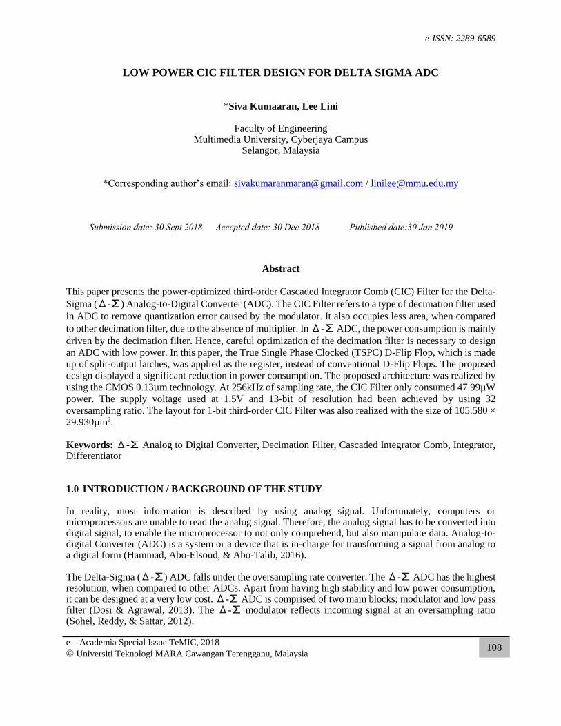
On the other hand, the low pass filter or also known as digital filter down samples the modulated signal to the actual frequency. It also filters out quantization noise from the modulated signal. Quantization noise takes place due to the inability of the ADC to convert analog signal into digital signal. There are always variances in analog and digital values. These differences may lead to distortion or quantization error (Babu, Shesharaman, & Kittur, 2012). Digital filter uses noise shaping and low pass filtering methods to filter out errors (Sohel, Reddy, & Sattar, 2012). In 1981, Eugene Hogenauer proposed the Cascaded Integrator Comb (CIC) filter. CIC refers to a type of digital filter that is comprised of an integrator and a differentiator, which is also known as comb (Hogenauer, 1981). The transfer function of CIC is given by the following equation:
𝑯(𝒛) = (𝟏−𝒁−𝑲
𝟏−𝒁−𝟏)𝑳
(1)
Where, L is CIC filter order and K is oversampling ratio. The numerator of Eq (1) shows the comb, while the denominator of Eq (3) represents the integrator. Furthermore, Eq (1) displays that all coefficients are equivalent to one. Hence, no multiplier is required to design the CIC filter. In fact, this is the main advantage of the CIC filter that generates low consumption power. Fig. 1 illustrates the block diagram of the first-order CIC (Ramesh, Nagarjuna, & Raam, 2011). To date, hand-held devices, portable communications, voice-over internet protocol (VOIP), and medical devices imply the rapidly growing demand for a wide range of consumer application. Besides, these devices must be power-efficient for operation at low voltage to enhance the longevity of battery. As for Δ-∑ ADC, the power is largely governed by decimation filter. Thus, a power-optimized decimation filter in essential in our daily lives (Sohel, Reddy, & Sattar, 2012). In this paper, a low-power third-order CIC filter with 13-bit resolution is proposed. The sampling frequency, fs, applied to design the CIC filter was 256kHz (Hammad, Abo-Elsoud, & Abo-Talib, 2016).
Figure 1 First-Order CIC Filter (Ramesh, Nagarjuna, & Raam, 2011)
2.0 LITERATURE STUDY
e-ISSN: 2289-6589
e – Academia Special Issue TeMIC, 2018
© Universiti Teknologi MARA Cawangan Terengganu, Malaysia
110
2.1 Design Specification
Prior to designing the CIC filter, certain specifications were set, such as sampling frequency (fs), decimation
factor or oversampling ratio (K), order of CIC filter (L), total output bits (P), and the required resolution
(N). The sampling frequency and the decimation factor must be similar to the modulator. Meanwhile, the
order of CIC filter must be higher than the Δ-∑ modulator (Teymourzadeh & Othman, 2006). This is
represented in the following equation:
𝑳 > 𝑶𝒓𝒅𝒆𝒓 𝒐𝒇 𝚫 − ∑ 𝑴𝒐𝒅𝒖𝒍𝒂𝒕𝒐𝒓 (2)
Next, the total output bits, P, was generated by the CIC filter by using the following equation:
𝑷 = 𝑳 ∗ 𝒍𝒐𝒈𝟐𝑲 + 𝑩𝒊𝒏 + 𝟏 𝒔𝒊𝒈𝒏 𝒃𝒊𝒕 (3)
Where, Bin is input bit to the CIC filter. The input bit is usually one (Teymourzadeh & Othman, 2006).
Besides, the actual required bits, N, as calculated via the equation given below:
𝑵 =𝟓𝟎𝒍𝒐𝒈𝑲−𝟏𝟐.𝟗
𝟔.𝟎𝟐 (4)
If the total output bits, P, is bigger than the actual required bits, N, the remaining number bits (LSB) must
be discarded upon calculating the final output (Hammad, Abo-Elsoud, & Abo-Talib, 2016). The design
specification used to design the CIC filter proposed in this paper is presented in Table 1.
Table 1 Specification of CIC filter
Aspect Value
Sampling frequency (fs) 256kHz
Decimation factor (K) 32
Order of the CIC filter (L) 3rd order
Total output bits (P) 17-bits
Actual needed resolution (N) 13-bits
Discarded bits 4-bits
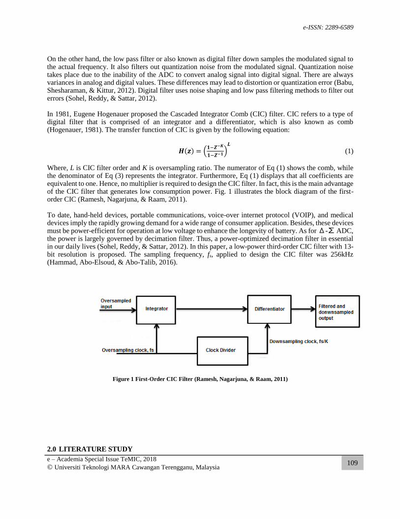
Fig. 2 illustrates the block diagram of third-order CIC filter implementation (Babu, Shesharaman, & Kittur,
2012). Three 17 integrators are cascaded with the three 17 differentiators to form the architecture.
e-ISSN: 2289-6589
e – Academia Special Issue TeMIC, 2018
© Universiti Teknologi MARA Cawangan Terengganu, Malaysia
111
Figure 2 Block Diagram of Third-Order CIC Filter (Babu, Shesharaman, & Kittur, 2012)
2.2 Coder Circuit
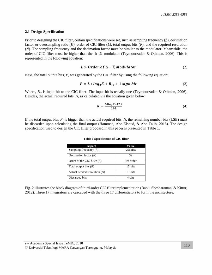
The coder circuit is typically used to increase the resolution of CIC filter. In this paper, the coder circuit
aids the CIC to achieve 17-bit from 1-bit input. This is used to implement the 2’s complement method so
as to avoid the register overflow and to overcome lost information. Register overflow occurs because the
register used in the integrator is incapable of holding huge amount of data at a time. The 2’s complement
method doubles the capacity of the register to store data as it represents the data for both positive and
negative data (Lata & Duhan). Fig. 3 portrays the architecture of coder circuit. Table 2 shows the outputs
for the given inputs.
Figure 3 Coder Circuit (Lata & Duhan)
e-ISSN: 2289-6589
e – Academia Special Issue TeMIC, 2018
© Universiti Teknologi MARA Cawangan Terengganu, Malaysia
112
Table 2 Input and output of the coder circuit
Input (1-bit) Output (17-bits)
1 00000000000000001
0 11111111111111111
2.3 Integrator
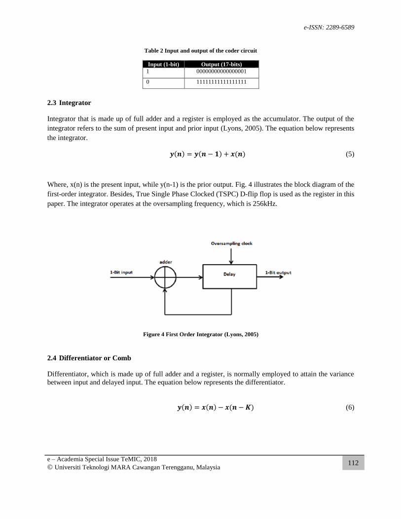
Integrator that is made up of full adder and a register is employed as the accumulator. The output of the
integrator refers to the sum of present input and prior input (Lyons, 2005). The equation below represents
the integrator.
𝒚(𝒏) = 𝒚(𝒏 − 𝟏) + 𝒙(𝒏) (5)
Where, x(n) is the present input, while y(n-1) is the prior output. Fig. 4 illustrates the block diagram of the
first-order integrator. Besides, True Single Phase Clocked (TSPC) D-flip flop is used as the register in this
paper. The integrator operates at the oversampling frequency, which is 256kHz.
Figure 4 First Order Integrator (Lyons, 2005)
2.4 Differentiator or Comb
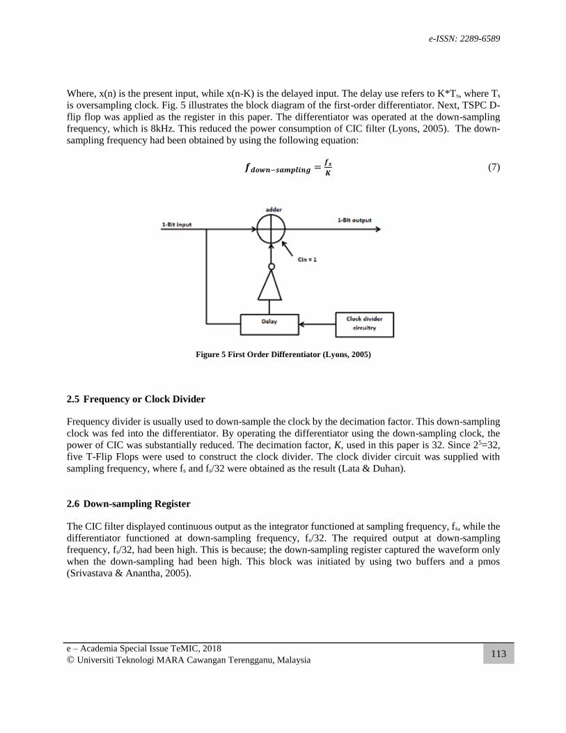
Differentiator, which is made up of full adder and a register, is normally employed to attain the variance
between input and delayed input. The equation below represents the differentiator.
𝒚(𝒏) = 𝒙(𝒏) − 𝒙(𝒏 − 𝑲) (6)
e-ISSN: 2289-6589
e – Academia Special Issue TeMIC, 2018
© Universiti Teknologi MARA Cawangan Terengganu, Malaysia
113
Where, x(n) is the present input, while x(n-K) is the delayed input. The delay use refers to K*Ts, where Ts
is oversampling clock. Fig. 5 illustrates the block diagram of the first-order differentiator. Next, TSPC D-
flip flop was applied as the register in this paper. The differentiator was operated at the down-sampling
frequency, which is 8kHz. This reduced the power consumption of CIC filter (Lyons, 2005). The down-
sampling frequency had been obtained by using the following equation:
𝒇𝒅𝒐𝒘𝒏−𝒔𝒂𝒎𝒑𝒍𝒊𝒏𝒈 =𝒇𝒔
𝑲 (7)
Figure 5 First Order Differentiator (Lyons, 2005)
2.5 Frequency or Clock Divider
Frequency divider is usually used to down-sample the clock by the decimation factor. This down-sampling
clock was fed into the differentiator. By operating the differentiator using the down-sampling clock, the
power of CIC was substantially reduced. The decimation factor, K, used in this paper is 32. Since 25=32,
five T-Flip Flops were used to construct the clock divider. The clock divider circuit was supplied with
sampling frequency, where fs and fs/32 were obtained as the result (Lata & Duhan).
2.6 Down-sampling Register
The CIC filter displayed continuous output as the integrator functioned at sampling frequency, fs, while the
differentiator functioned at down-sampling frequency, fs/32. The required output at down-sampling
frequency, fs/32, had been high. This is because; the down-sampling register captured the waveform only
when the down-sampling had been high. This block was initiated by using two buffers and a pmos
(Srivastava & Anantha, 2005).
e-ISSN: 2289-6589
e – Academia Special Issue TeMIC, 2018
© Universiti Teknologi MARA Cawangan Terengganu, Malaysia
114
3.0 METHODOLOGY
3.1 The Proposed Design
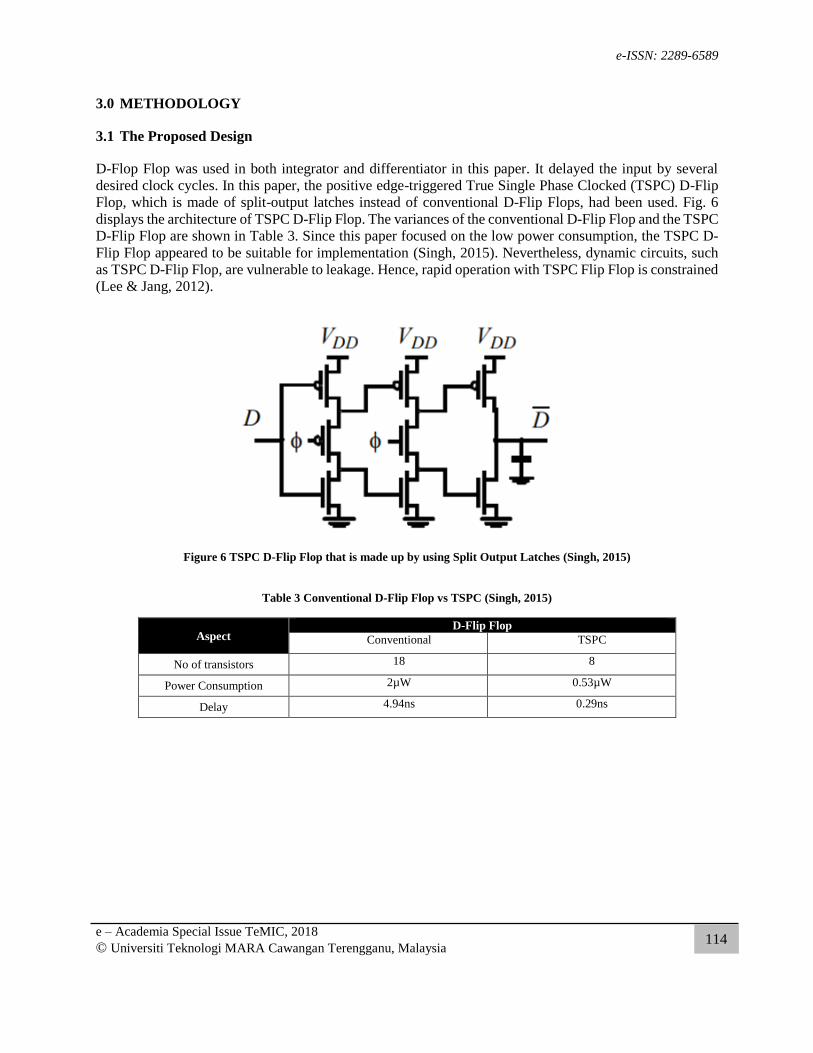
D-Flop Flop was used in both integrator and differentiator in this paper. It delayed the input by several
desired clock cycles. In this paper, the positive edge-triggered True Single Phase Clocked (TSPC) D-Flip
Flop, which is made of split-output latches instead of conventional D-Flip Flops, had been used. Fig. 6
displays the architecture of TSPC D-Flip Flop. The variances of the conventional D-Flip Flop and the TSPC
D-Flip Flop are shown in Table 3. Since this paper focused on the low power consumption, the TSPC D-
Flip Flop appeared to be suitable for implementation (Singh, 2015). Nevertheless, dynamic circuits, such
as TSPC D-Flip Flop, are vulnerable to leakage. Hence, rapid operation with TSPC Flip Flop is constrained
(Lee & Jang, 2012).
Figure 6 TSPC D-Flip Flop that is made up by using Split Output Latches (Singh, 2015)
Table 3 Conventional D-Flip Flop vs TSPC (Singh, 2015)
Aspect D-Flip Flop
Conventional TSPC
No of transistors 18 8
Power Consumption 2µW 0.53µW
Delay 4.94ns 0.29ns
e-ISSN: 2289-6589
e – Academia Special Issue TeMIC, 2018
© Universiti Teknologi MARA Cawangan Terengganu, Malaysia
115
4.0 RESULT AND DISCUSSION
4.1 Integrator
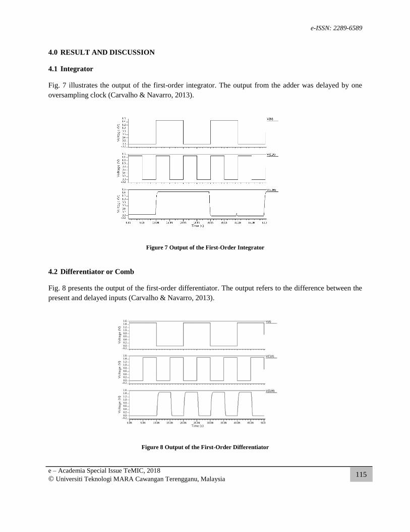
Fig. 7 illustrates the output of the first-order integrator. The output from the adder was delayed by one
oversampling clock (Carvalho & Navarro, 2013).
Figure 7 Output of the First-Order Integrator
4.2 Differentiator or Comb
Fig. 8 presents the output of the first-order differentiator. The output refers to the difference between the
present and delayed inputs (Carvalho & Navarro, 2013).
Figure 8 Output of the First-Order Differentiator
e-ISSN: 2289-6589
e – Academia Special Issue TeMIC, 2018
© Universiti Teknologi MARA Cawangan Terengganu, Malaysia
116
4.3 CIC Filter Output
2KHz of sine wave with the value of 0.6Vpp was applied to ADC. The output occurred at the down-sampling
frequency, which is 8KHz. The output was in 2’s complement form with 17 bits. Therefore, the 2’s
complement had been converted into decimal after discarding the lowest 4 bits. In order to compare the
result with analog equivalent, the decimal value was multiplied with the following equation (Teymourzadeh
& Othman, An Enhancement of Decimation Process using Fast Cascaded Integrator Comb (CIC) Filter,
2006):
𝟏𝑳𝑺𝑩 =𝑽𝑭𝑺𝑹
𝟐𝑵 (8)
Where, VFSR is the full-scale voltage range of the input signal, while N is the number of output bits. In this
paper, VFSR=0.6V and N=13 had been achieved.
Fig. 10 illustrates the output from CIC Filter. From 17 bits, 4 bits were discarded, making the final output
as 13 bits. The output obtained is summarized in Table 4.
Table 4 Output of CIC filter
2’s Complement Decimal Analog Equivalent
0011101000100 1860 0.1362V
0101011100010 2786 0.2041V
1110100111101 -707 -0.0518V
1011100011001 -2279 -0.1669V
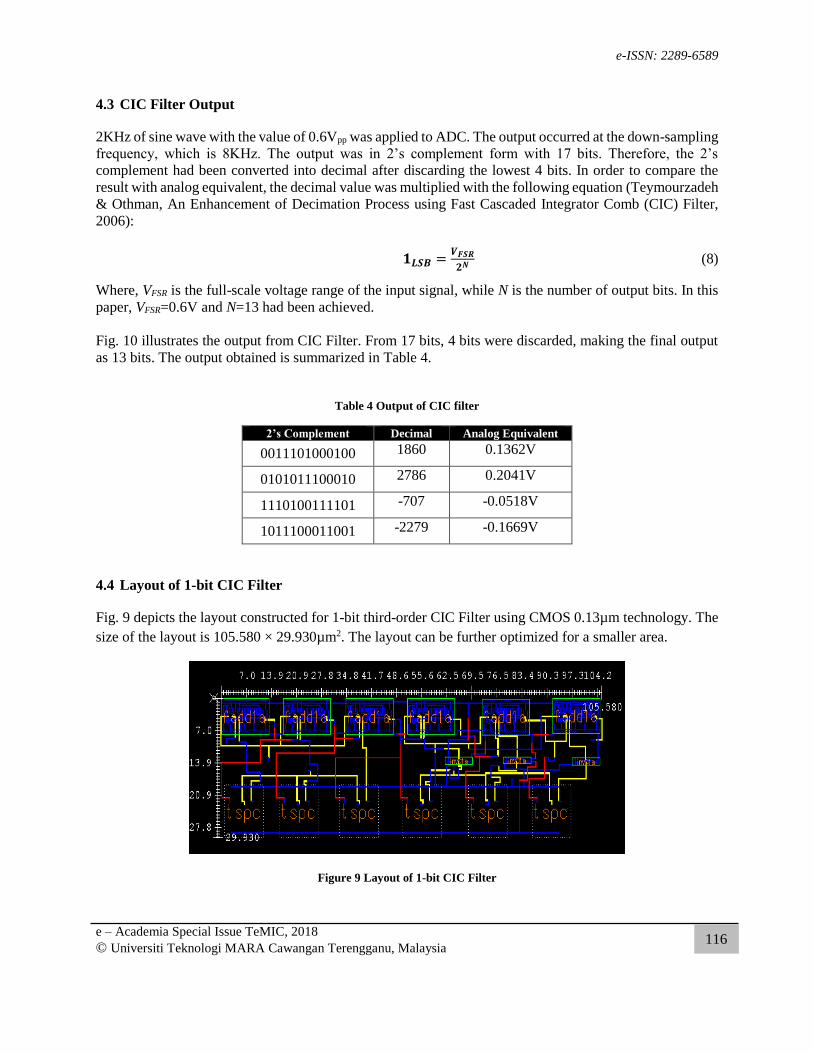
4.4 Layout of 1-bit CIC Filter
Fig. 9 depicts the layout constructed for 1-bit third-order CIC Filter using CMOS 0.13µm technology. The
size of the layout is 105.580 × 29.930µm2. The layout can be further optimized for a smaller area.
Figure 9 Layout of 1-bit CIC Filter
e-ISSN: 2289-6589
e – Academia Special Issue TeMIC, 2018
© Universiti Teknologi MARA Cawangan Terengganu, Malaysia
117
4.5 Comparison with Related Works
Table 5 displays a comparison between the proposed work and other related studies. This work is realized
using 0.13µm CMOS technology and has total of 17 output bits. This work records the least amount of
power consumption at 1.5V with the usage of TSPC D-Flip Flop as the register in the integrator and
differentiator. However, it is also noted that the sampling rate is lower compared to others to meet the
requirement of the ADC.
Table 5 Comparison with related works
Ref.
(Babu,
Shesharaman,
& Kittur,
2012)
(Sohel,
Reddy, &
Sattar,
2012)
(Carvalho &
Navarro,
2013)
(Teymourzadeh & Othman,
An Enhancement of
Decimation Process using
Fast Cascaded Integrator
Comb (CIC) Filter, 2006)
This Work
Technology
(µm) 0.18 - 0.14 0.18 0.13
Resolution
(bits) 16 14 16 16 13
Sampling Rate
(Hz)
16.8G 256k 2048k 190M 256k
Supply Voltage
(V)
1.5 1.4 0.9 - 1.5
Power
(W)
2.67m 238µ 188µ 3.5m 47.99 µ
Figure 10 Output of CIC Filter
e-ISSN: 2289-6589
e – Academia Special Issue TeMIC, 2018
© Universiti Teknologi MARA Cawangan Terengganu, Malaysia
118
5.0 CONCLUSION AND FUTURE WORKS
The third-order 13-bit CIC Filter with an oversampling ratio of 32 for Δ-∑ ADC had been designed successfully in this paper. The decimation filter consists of coder circuit, integrator, differentiator, clock divider, and down-sampling register. The CIC filter was implemented by using CMOS 0.13µm technology. It used only 47.99µW of power from 1.5V supply voltage. The layout for 1-bit third-order CIC Filter is also realized with the size of 105.580 × 29.930µm2. The usage of positive-triggered TSPC D-Flip Flop in the integrator and differentiator substantially contributed to reduce power consumption of the decimation filter. After completing this project, there are few areas in which this work can be enhanced for a better reliability and performance factor. Among are, the adder in the integrator and differentiator can be optimized to reduce the power consumption. Furthermore, A full layout for 17-bit CIC Filter can be realized. Acknowledgement The authors would like to thank all who have made this project a successful one.
References
Babu, B., Shesharaman, K. N., & Kittur, H. M. (2012). Power Optimised Digital Decimation Filter for
Medical Applications. International Conference on Advances in Computing and Communications,
90-93.
Carvalho, D. D., & Navarro, J. (2013). A power optimized decimator for sigma-delta data converters. 2013
IEEE 4th Latin American Symposium on Circuits and Systems (LASCAS), 1-4.
doi:10.1109/lascas.2013.6519018
Dosi, H., & Agrawal, R. (2013). Low Power 8 bit Analog to Digital Converter (ADC) in 180nm CMOS
Technology. International Journal of Science and Research (IJSR), 2(7), 417-418.
Hammad, A. O., Abo-Elsoud, M. A., & Abo-Talib, A. M. (2016). VHDL-AMS Model for Switched
Resistor Delta Sigma Modulator. International Journal of Science and Research (IJSR), 5(11), 587-
591. doi:10.21275/ART20162806
Hogenauer, E. (1981). An economical class of digtal filters for decimation and interpolation. IEEE
transactions on acoustics, speech, and signal processing, 29(2), 155-162.
Lata, K., & Duhan, M. (n.d.). Design of a Decimator Filter for Novel Sigma-Delta Modulator. IOSR Journal
of VLSI and Signal Processing (IOSR-JVSP), 2, 31-37.
Lee, H. Y., & Jang, Y. C. (2012). A true single-phase clocked flip-flop with leakage current compensation.
IEICE Electronics Express, 9(23), 1807-1812.
Lyons, R. (2005). Understanding cascaded integrator-comb filters. Embed Syst Program, 18(4), 14-27.
e-ISSN: 2289-6589
e – Academia Special Issue TeMIC, 2018
© Universiti Teknologi MARA Cawangan Terengganu, Malaysia
119
Ramesh, A. P., Nagarjuna, G., & Raam, G. S. (2011). FPGA based design and implementation of higher
order FIR filter using improved DA algorithm. International Journal of Computer Applications,
35(9), 45-54.
Singh, H. K. (2015). Design and Analysis of D Flip Flop Using Different Technologies. International
Journal of Innovative Research in Computer and Communication Engineering, 3(7), 6919-6926.
doi:10.15680/ijircce.2015.0307050
Sohel, M. A., Reddy, K. C., & Sattar, S. A. (2012). Design of Low Power Sigma Delta ADC. International
Journal of VLSI Design & Communication Systems, 3(4), 67.
Srivastava, A., & Anantha, R. R. (2005). A programmable oversampling sigma-delta analog-to-digital
converter. Circuits and Systems, 2005. 48th Midwest Symposium, 539-542.
Teymourzadeh, R., & Othman, M. (2006). VLSI Implementation of Cascaded Integrator Comb Filters for
DSP Applications. 4th National Technical Postgraduate Symposium, TechPos 2006, 54-58.
Teymourzadeh, R., & Othman, M. B. (2006). An Enhancement of Decimation Process using Fast Cascaded
Integrator Comb (CIC) Filter. 2006 IEEE International Conference on Semiconductor Electronics,
811-815. doi:10.1109/smelec.2006.380749