Low Input Voltage, 0.7V, Boost Converter With 5.5μA ... · TPS61222-EP SLVSBI2 – SEPTEMBER 2012...
20
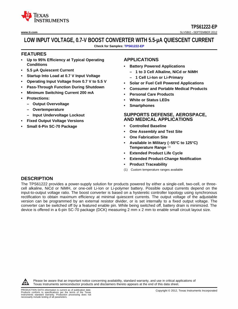
TPS61222-EP www.ti.com SLVSBI2 – SEPTEMBER 2012 LOW INPUT VOLTAGE, 0.7-V BOOST CONVERTER WITH 5.5-μA QUIESCENT CURRENT Check for Samples: TPS61222-EP 1FEATURES • Up to 95% Efficiency at Typical Operating APPLICATIONS Conditions • Battery Powered Applications • 5.5 μA Quiescent Current – 1 to 3 Cell Alkaline, NiCd or NiMH • Startup Into Load at 0.7 V Input Voltage – 1 Cell Li-Ion or Li-Primary • Operating Input Voltage from 0.7 V to 5.5 V • Solar or Fuel Cell Powered Applications • Pass-Through Function During Shutdown • Consumer and Portable Medical Products • Minimum Switching Current 200 mA • Personal Care Products • Protections: • White or Status LEDs – Output Overvoltage • Smartphones – Overtemperature SUPPORTS DEFENSE, AEROSPACE, – Input Undervoltage Lockout AND MEDICAL APPLICATIONS • Fixed Output Voltage Versions • Controlled Baseline • Small 6-Pin SC-70 Package • One Assembly and Test Site • One Fabrication Site • Available in Military (–55°C to 125°C) Temperature Range (1) • Extended Product Life Cycle • Extended Product-Change Notification • Product Traceability (1) Custom temperature ranges available DESCRIPTION The TPS61222 provides a power-supply solution for products powered by either a single-cell, two-cell, or three- cell alkaline, NiCd or NiMH, or one-cell Li-Ion or Li-polymer battery. Possible output currents depend on the input-to-output voltage ratio. The boost converter is based on a hysteretic controller topology using synchronous rectification to obtain maximum efficiency at minimal quiescent currents. The output voltage of the adjustable version can be programmed by an external resistor divider, or is set internally to a fixed output voltage. The converter can be switched off by a featured enable pin. While being switched off, battery drain is minimized. The device is offered in a 6-pin SC-70 package (DCK) measuring 2 mm x 2 mm to enable small circuit layout size. 1 Please be aware that an important notice concerning availability, standard warranty, and use in critical applications of Texas Instruments semiconductor products and disclaimers thereto appears at the end of this data sheet. PRODUCTION DATA information is current as of publication date. Copyright © 2012, Texas Instruments Incorporated Products conform to specifications per the terms of the Texas Instruments standard warranty. Production processing does not necessarily include testing of all parameters.
-
Upload
nguyendien -
Category
Documents
-
view
216 -
download
0
Transcript of Low Input Voltage, 0.7V, Boost Converter With 5.5μA ... · TPS61222-EP SLVSBI2 – SEPTEMBER 2012...
TPS61222-EPwww.ti.com SLVSBI2 –SEPTEMBER 2012
LOW INPUT VOLTAGE, 0.7-V BOOST CONVERTER WITH 5.5-μA QUIESCENT CURRENTCheck for Samples: TPS61222-EP
1FEATURES• Up to 95% Efficiency at Typical Operating APPLICATIONS
Conditions • Battery Powered Applications• 5.5 μA Quiescent Current – 1 to 3 Cell Alkaline, NiCd or NiMH• Startup Into Load at 0.7 V Input Voltage – 1 Cell Li-Ion or Li-Primary• Operating Input Voltage from 0.7 V to 5.5 V • Solar or Fuel Cell Powered Applications• Pass-Through Function During Shutdown • Consumer and Portable Medical Products• Minimum Switching Current 200 mA • Personal Care Products• Protections: • White or Status LEDs
– Output Overvoltage • Smartphones– Overtemperature
SUPPORTS DEFENSE, AEROSPACE,– Input Undervoltage LockoutAND MEDICAL APPLICATIONS• Fixed Output Voltage Versions• Controlled Baseline• Small 6-Pin SC-70 Package• One Assembly and Test Site• One Fabrication Site• Available in Military (–55°C to 125°C)
Temperature Range (1)
• Extended Product Life Cycle• Extended Product-Change Notification• Product Traceability(1) Custom temperature ranges available
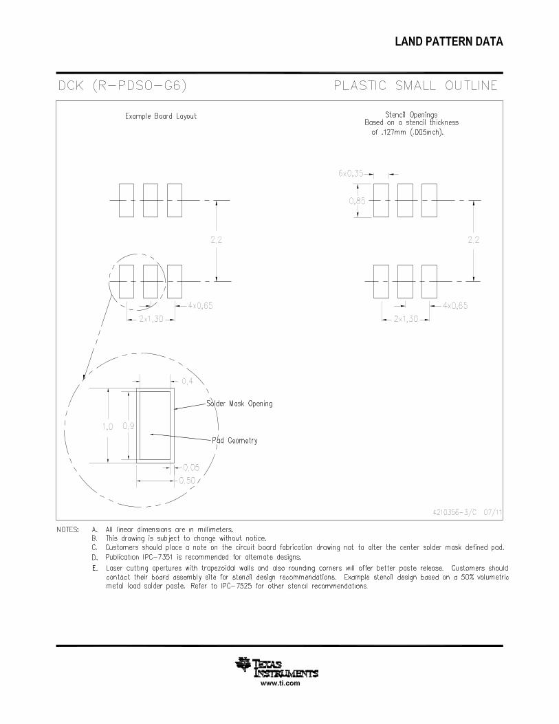
DESCRIPTIONThe TPS61222 provides a power-supply solution for products powered by either a single-cell, two-cell, or three-cell alkaline, NiCd or NiMH, or one-cell Li-Ion or Li-polymer battery. Possible output currents depend on theinput-to-output voltage ratio. The boost converter is based on a hysteretic controller topology using synchronousrectification to obtain maximum efficiency at minimal quiescent currents. The output voltage of the adjustableversion can be programmed by an external resistor divider, or is set internally to a fixed output voltage. Theconverter can be switched off by a featured enable pin. While being switched off, battery drain is minimized. Thedevice is offered in a 6-pin SC-70 package (DCK) measuring 2 mm x 2 mm to enable small circuit layout size.
1
Please be aware that an important notice concerning availability, standard warranty, and use in critical applications ofTexas Instruments semiconductor products and disclaimers thereto appears at the end of this data sheet.
PRODUCTION DATA information is current as of publication date. Copyright © 2012, Texas Instruments IncorporatedProducts conform to specifications per the terms of the TexasInstruments standard warranty. Production processing does notnecessarily include testing of all parameters.
TPS61222-EPSLVSBI2 –SEPTEMBER 2012 www.ti.com
This integrated circuit can be damaged by ESD. Texas Instruments recommends that all integrated circuits be handled withappropriate precautions. Failure to observe proper handling and installation procedures can cause damage.
ESD damage can range from subtle performance degradation to complete device failure. Precision integrated circuits may be moresusceptible to damage because very small parametric changes could cause the device not to meet its published specifications.
AVAILABLE DEVICE OPTIONS (1)
PACKAGETJ PACKAGE (2) PART NUMBER VID NUMBER
MARKING
–55°C to 125°C SHL 6-Pin SC-70 TPS61222MDCKTEP V62/12603-01XE
(1) Contact the factory to check availability of other fixed output voltage versions.(2) For the most current package and ordering information, see the Package Option Addendum at the end of this document, or see the TI
website at www.ti.com.
ABSOLUTE MAXIMUM RATINGSover operating free-air temperature range (unless otherwise noted) (1)
UNIT
VIN Input voltage range on VIN, L, VOUT, EN, FB –0.3 to 7.5 V
TJ Operating junction temperature range –55 to 145 °C
Tstg Storage temperature range –65 to 150 °C
Human Body Model (HBM) (2) 2 kV
ESD Machine Model (MM) (2) 200 V
Charged Device Model (CDM) (2) 1.5 kV
(1) Stresses beyond those listed under Absolute Maximum Ratings may cause permanent damage to the device. These are stress ratingsonly, and functional operation of the device at these or any other conditions beyond those indicated under Recommended OperatingConditions is not implied. Exposure to absolute-maximum-rated conditions for extended periods may affect device reliability.
(2) ESD testing is performed according to the respective JESD22 JEDEC standard.
THERMAL INFORMATIONTPS61222
THERMAL METRIC (1) DCK UNITS
6 PINS
θJA Junction-to-ambient thermal resistance (2) 231.2
θJCtop Junction-to-case (top) thermal resistance (3) 61.8
θJB Junction-to-board thermal resistance (4) 78.8°C/W
ψJT Junction-to-top characterization parameter (5) 2.2
ψJB Junction-to-board characterization parameter (6) 78
θJCbot Junction-to-case (bottom) thermal resistance (7) N/A
(1) For more information about traditional and new thermal metrics, see the IC Package Thermal Metrics application report, SPRA953.(2) The junction-to-ambient thermal resistance under natural convection is obtained in a simulation on a JEDEC-standard, high-K board, as
specified in JESD51-7, in an environment described in JESD51-2a.(3) The junction-to-case (top) thermal resistance is obtained by simulating a cold plate test on the package top. No specific JEDEC-
standard test exists, but a close description can be found in the ANSI SEMI standard G30-88.(4) The junction-to-board thermal resistance is obtained by simulating in an environment with a ring cold plate fixture to control the PCB
temperature, as described in JESD51-8.(5) The junction-to-top characterization parameter, ψJT, estimates the junction temperature of a device in a real system and is extracted
from the simulation data for obtaining θJA, using a procedure described in JESD51-2a (sections 6 and 7).(6) The junction-to-board characterization parameter, ψJB, estimates the junction temperature of a device in a real system and is extracted
from the simulation data for obtaining θJA , using a procedure described in JESD51-2a (sections 6 and 7).(7) The junction-to-case (bottom) thermal resistance is obtained by simulating a cold plate test on the exposed (power) pad. No specific
JEDEC standard test exists, but a close description can be found in the ANSI SEMI standard G30-88.Spacer
2 Submit Documentation Feedback Copyright © 2012, Texas Instruments Incorporated
Product Folder Links :TPS61222-EP
TPS61222-EPwww.ti.com SLVSBI2 –SEPTEMBER 2012
RECOMMENDED OPERATING CONDITIONSMIN NOM MAX UNIT
VIN Supply voltage at VIN 0.7 5.5 V
TJ Operating free air temperature range –55 125 °C
ELECTRICAL CHARACTERISTICSTJ = −55°C to 125°C, TJ = TA and over recommended input voltage range (typical at an ambient temperature range of 25°C)(unless otherwise noted)
DC/DC STAGE
PARAMETER TEST CONDITIONS MIN TYP MAX UNIT
VIN Input voltage range 0.7 5.5 V
VIN Minimum input voltage at startup RLoad ≥ 150 Ω 0.7 V
VOUT Output voltage (5 V) VIN < VOUT 4.8 5 5.19 V
ILH Inductor current ripple 200 mA
ISW Switch current limit VOUT = 5 V, VIN = 1.2 V 200 400 mA
RDSon_HSD Rectifying switch on resistance VOUT = 5 V 700 mΩRDSon_LSD Main switch on resistance VOUT = 5 V 550 mΩ
Line regulation VIN < VOUT 0.5 %
Load regulation VIN < VOUT 0.5 %
VIN 0.5 1.4 μAQuiescentIQ IO = 0 mA, VEN = VIN = 1.2 V, VOUT = 5 Vcurrent VOUT 5 8.5 μA
ShutdownISD VIN VEN = 0 V, VIN = 1.2 V, VOUT ≥ VIN 0.2 0.96 μAcurrent
ILKG_L Leakage current into L VEN = 0 V, VIN = 1.2 V, VL = 1.2 V, VOUT ≥ VIN 0.01 0.3 μA
IEN EN input current Clamped on GND or VIN (VIN < 1.5 V) 0.005 0.13 μA
CONTROL STAGE
PARAMETER TEST CONDITIONS MIN TYP MAX UNIT
VIL EN input low voltage VIN ≤ 1.5 V 0.15 × VIN V
VIH EN input high voltage VIN ≤ 1.5 V 0.8 × VIN V
VIL EN input low voltage 5 V > VIN > 1.5 V 0.34 V
VIH EN input high voltage 5 V > VIN > 1.5 V 1.28 V
VUVLO Undervoltage lockout threshold for turn off VIN decreasing 0.5 0.72 V
Overvoltage protection threshold 5.5 7.5 V
Overtemperature protection 140 °C
Overtemperature hysteresis 20 °C
Copyright © 2012, Texas Instruments Incorporated Submit Documentation Feedback 3
Product Folder Links :TPS61222-EP
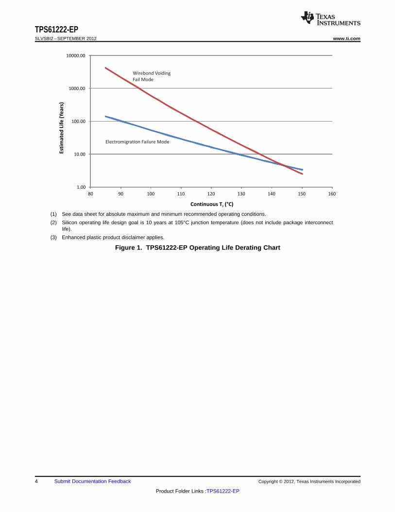
1.00
10.00
100.00
1000.00
10000.00
80 90 100 110 120 130 140 150 160
Est
ima
ted
Lif
e (
Ye
ars
)
Continuous T (°C)J
Electromigration Failure Mode
Wirebond Voiding
Fail Mode
TPS61222-EPSLVSBI2 –SEPTEMBER 2012 www.ti.com
(1) See data sheet for absolute maximum and minimum recommended operating conditions.
(2) Silicon operating life design goal is 10 years at 105°C junction temperature (does not include package interconnectlife).
(3) Enhanced plastic product disclaimer applies.
Figure 1. TPS61222-EP Operating Life Derating Chart
4 Submit Documentation Feedback Copyright © 2012, Texas Instruments Incorporated
Product Folder Links :TPS61222-EP
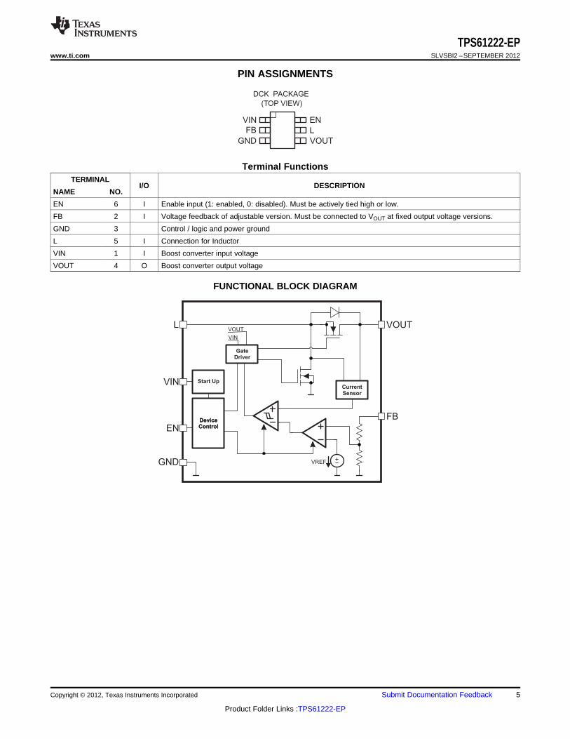
CurrentSensor
GateDriver
DeviceControl
GND
EN
FB
VOUTL
VREF
VIN
DeviceControl
Start Up
VIN
VOUT
GND
L
VIN EN
VOUT
FB
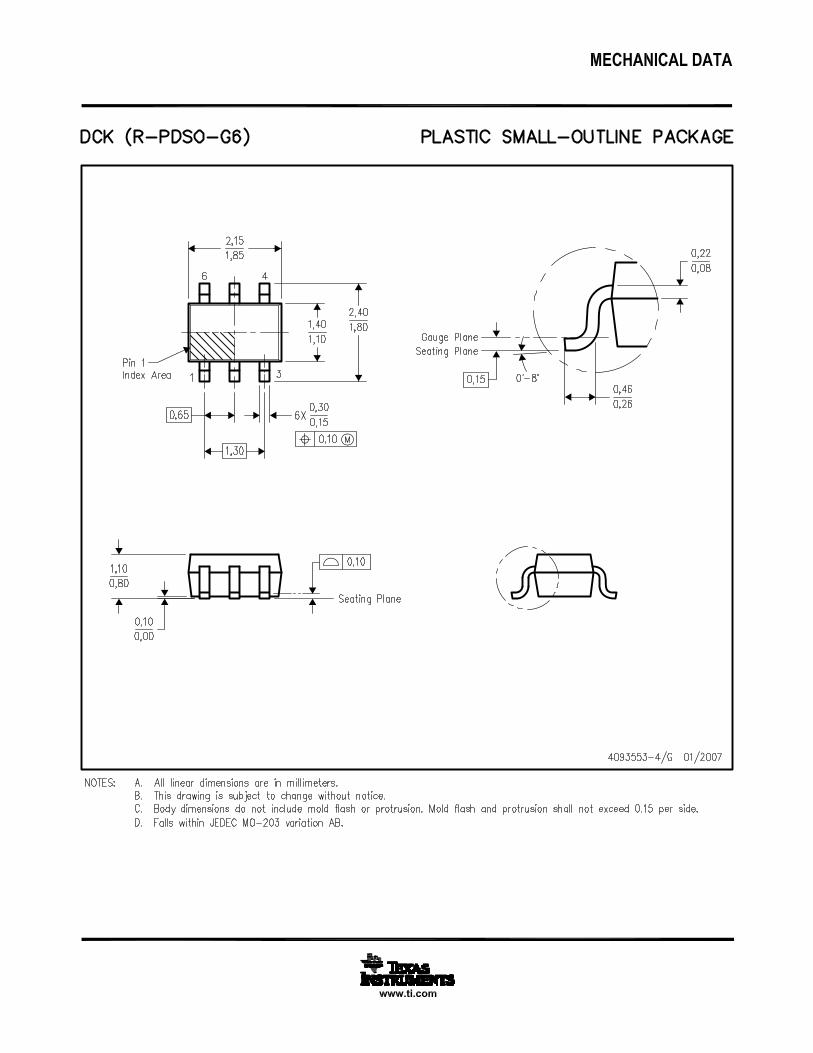
DCK PACKAGE
(TOP VIEW)
TPS61222-EPwww.ti.com SLVSBI2 –SEPTEMBER 2012
PIN ASSIGNMENTS
Terminal FunctionsTERMINAL
I/O DESCRIPTIONNAME NO.
EN 6 I Enable input (1: enabled, 0: disabled). Must be actively tied high or low.
FB 2 I Voltage feedback of adjustable version. Must be connected to VOUT at fixed output voltage versions.
GND 3 Control / logic and power ground
L 5 I Connection for Inductor
VIN 1 I Boost converter input voltage
VOUT 4 O Boost converter output voltage
FUNCTIONAL BLOCK DIAGRAM
Copyright © 2012, Texas Instruments Incorporated Submit Documentation Feedback 5
Product Folder Links :TPS61222-EP
L
L1
VIN
VOUT
FB C2
EN
GND
TPS6122x
VOUT
R1
R2
VIN
C1
TPS61222-EPSLVSBI2 –SEPTEMBER 2012 www.ti.com
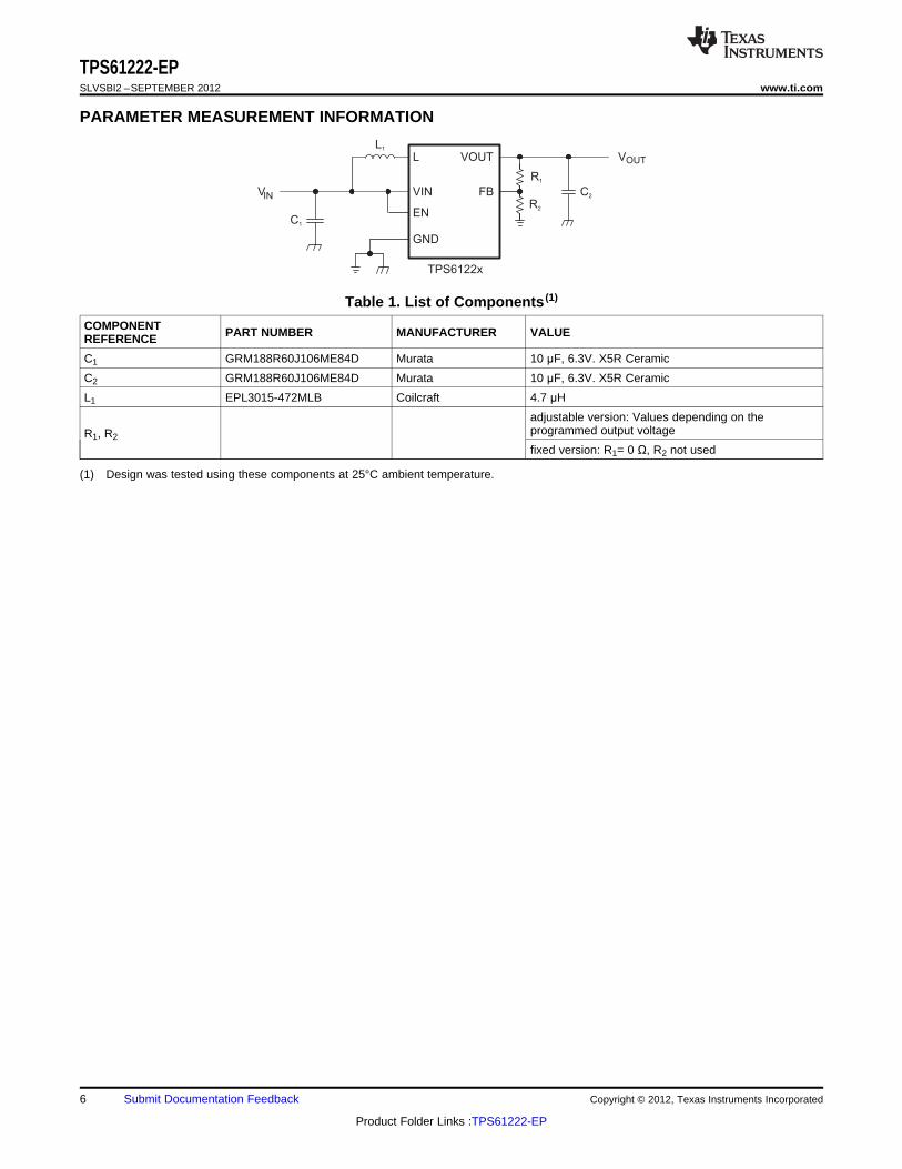
PARAMETER MEASUREMENT INFORMATION
Table 1. List of Components (1)
COMPONENT PART NUMBER MANUFACTURER VALUEREFERENCE
C1 GRM188R60J106ME84D Murata 10 μF, 6.3V. X5R Ceramic
C2 GRM188R60J106ME84D Murata 10 μF, 6.3V. X5R Ceramic
L1 EPL3015-472MLB Coilcraft 4.7 μH
adjustable version: Values depending on theprogrammed output voltageR1, R2
fixed version: R1= 0 Ω, R2 not used
(1) Design was tested using these components at 25°C ambient temperature.
6 Submit Documentation Feedback Copyright © 2012, Texas Instruments Incorporated
Product Folder Links :TPS61222-EP
0
20
40
60
80
100
0.7 1.7 2.7 3.7 4.7
V - Input Voltage - VI
h-
Eff
icie
ncy -
%
I = 50 mAO
I = 100 AO
m
I = 10 mAO
I = 1 mAO
V = 5 VO
0
10
20
30
40
50
60
70
80
0.7 1.7 2.7 3.7 4.7
V - Input Voltage - VI
I-
Inp
ut
Cu
rren
t -
AI
m
V = 5 VO
Device Enabled
0
50
100
150
200
250
300
0.7 1.2 1.7 2.2 2.7 3.2 3.7 4.2 4.7
V - Input Voltage - VI
V = 5 VO
Maxim
um
ou
tpu
t C
urr
en
t -
mA
0
10
20
30
40
50
60
70
80
90
100
h-
Eff
icie
ncy -
%
0.01 0.1 1 10 100
I - Output Current - mAO
V = 0.7 VI
V = 1.2 VI
V = 4.2 VI
V = 5 VO
V = 2.4 VI
V = 3.6 VI
TPS61222-EPwww.ti.com SLVSBI2 –SEPTEMBER 2012
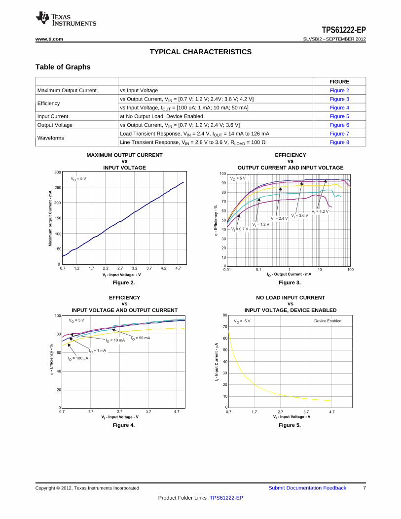
TYPICAL CHARACTERISTICS
Table of Graphs
FIGURE
Maximum Output Current vs Input Voltage Figure 2
vs Output Current, VIN = [0.7 V; 1.2 V; 2.4V; 3.6 V; 4.2 V] Figure 3Efficiency
vs Input Voltage, IOUT = [100 uA; 1 mA; 10 mA; 50 mA] Figure 4
Input Current at No Output Load, Device Enabled Figure 5
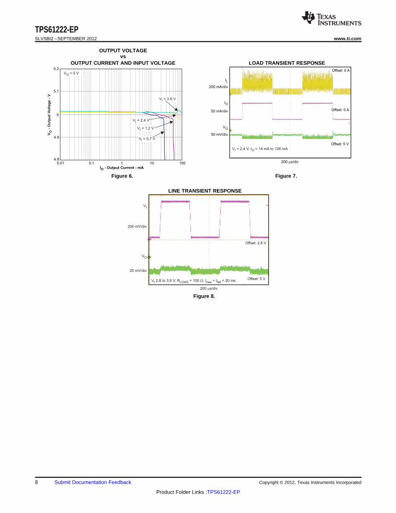
Output Voltage vs Output Current, VIN = [0.7 V; 1.2 V; 2.4 V; 3.6 V] Figure 6
Load Transient Response, VIN = 2.4 V, IOUT = 14 mA to 126 mA Figure 7Waveforms
Line Transient Response, VIN = 2.8 V to 3.6 V, RLOAD = 100 Ω Figure 8
MAXIMUM OUTPUT CURRENT EFFICIENCYvs vs
INPUT VOLTAGE OUTPUT CURRENT AND INPUT VOLTAGE
Figure 2. Figure 3.
EFFICIENCY NO LOAD INPUT CURRENTvs vs
INPUT VOLTAGE AND OUTPUT CURRENT INPUT VOLTAGE, DEVICE ENABLED
Figure 4. Figure 5.
Copyright © 2012, Texas Instruments Incorporated Submit Documentation Feedback 7
Product Folder Links :TPS61222-EP
VI
200 mV/div
VO
20 mV/div
Offset: 2.8 V
Offset: 5 V
200 s/divm
V 2.8 to 3.6 V, R = 100 , t = t = 20 msI LOAD rise fall
W
4.8
4.9
5
5.1
5.2
0.01 0.1 1 10 100
I - Output Current - mAO
V = 0.7 VI
V = 1.2 VI
V = 2.4 VI
V = 5 VO
V-
Ou
tpu
t V
olt
ag
e -
VO
V = 3.6 VI
VO
50 mV/div
200 mA/div
IL
200 s/divm
50 mA/div
IO
Offset: 0 A
Offset: 0 A
Offset: 5 V
V = 2.4 V, I = 14 mA to 126 mAI O
TPS61222-EPSLVSBI2 –SEPTEMBER 2012 www.ti.com
OUTPUT VOLTAGEvs
OUTPUT CURRENT AND INPUT VOLTAGE LOAD TRANSIENT RESPONSE
Figure 6. Figure 7.
LINE TRANSIENT RESPONSE
Figure 8.
8 Submit Documentation Feedback Copyright © 2012, Texas Instruments Incorporated
Product Folder Links :TPS61222-EP
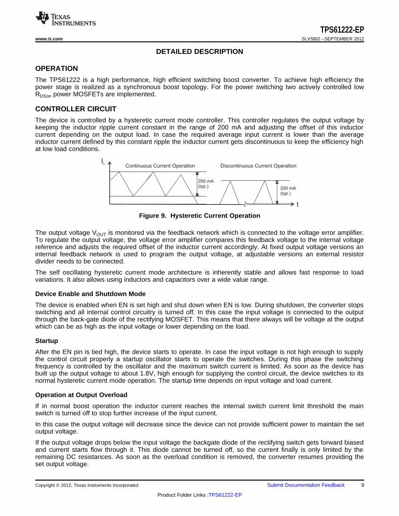
IL
t
200 mA(typ.)
Continuous Current Operation Discontinuous Current Operation
200 mA(typ.)
TPS61222-EPwww.ti.com SLVSBI2 –SEPTEMBER 2012
DETAILED DESCRIPTION
OPERATION
The TPS61222 is a high performance, high efficient switching boost converter. To achieve high efficiency thepower stage is realized as a synchronous boost topology. For the power switching two actively controlled lowRDSon power MOSFETs are implemented.
CONTROLLER CIRCUIT
The device is controlled by a hysteretic current mode controller. This controller regulates the output voltage bykeeping the inductor ripple current constant in the range of 200 mA and adjusting the offset of this inductorcurrent depending on the output load. In case the required average input current is lower than the averageinductor current defined by this constant ripple the inductor current gets discontinuous to keep the efficiency highat low load conditions.
Figure 9. Hysteretic Current Operation
The output voltage VOUT is monitored via the feedback network which is connected to the voltage error amplifier.To regulate the output voltage, the voltage error amplifier compares this feedback voltage to the internal voltagereference and adjusts the required offset of the inductor current accordingly. At fixed output voltage versions aninternal feedback network is used to program the output voltage, at adjustable versions an external resistordivider needs to be connected.
The self oscillating hysteretic current mode architecture is inherently stable and allows fast response to loadvariations. It also allows using inductors and capacitors over a wide value range.
Device Enable and Shutdown Mode
The device is enabled when EN is set high and shut down when EN is low. During shutdown, the converter stopsswitching and all internal control circuitry is turned off. In this case the input voltage is connected to the outputthrough the back-gate diode of the rectifying MOSFET. This means that there always will be voltage at the outputwhich can be as high as the input voltage or lower depending on the load.
Startup
After the EN pin is tied high, the device starts to operate. In case the input voltage is not high enough to supplythe control circuit properly a startup oscillator starts to operate the switches. During this phase the switchingfrequency is controlled by the oscillator and the maximum switch current is limited. As soon as the device hasbuilt up the output voltage to about 1.8V, high enough for supplying the control circuit, the device switches to itsnormal hysteretic current mode operation. The startup time depends on input voltage and load current.
Operation at Output Overload
If in normal boost operation the inductor current reaches the internal switch current limit threshold the mainswitch is turned off to stop further increase of the input current.
In this case the output voltage will decrease since the device can not provide sufficient power to maintain the setoutput voltage.
If the output voltage drops below the input voltage the backgate diode of the rectifying switch gets forward biasedand current starts flow through it. This diode cannot be turned off, so the current finally is only limited by theremaining DC resistances. As soon as the overload condition is removed, the converter resumes providing theset output voltage.
Copyright © 2012, Texas Instruments Incorporated Submit Documentation Feedback 9
Product Folder Links :TPS61222-EP
TPS61222-EPSLVSBI2 –SEPTEMBER 2012 www.ti.com
Undervoltage Lockout
An implemented undervoltage lockout function stops the operation of the converter if the input voltage dropsbelow the typical undervoltage lockout threshold. This function is implemented in order to prevent malfunctioningof the converter.
Overvoltage Protection
If, for any reason, the output voltage is not fed back properly to the input of the voltage amplifier, control of theoutput voltage will not work anymore. Therefore an overvoltage protection is implemented to avoid the outputvoltage exceeding critical values for the device and possibly for the system it is supplying. For this protection theTPS61222 output voltage is also monitored internally. In case it reaches the internally programmed threshold of6.5 V typically the voltage amplifier regulates the output voltage to this value.
If the TPS61222 is used to drive LEDs, this feature protects the circuit if the LED fails.
Overtemperature Protection
The device has a built-in temperature sensor which monitors the internal IC junction temperature. If thetemperature exceeds the programmed threshold (see electrical characteristics table), the device stops operating.As soon as the IC temperature has decreased below the programmed threshold, it starts operating again. Toprevent unstable operation close to the region of overtemperature threshold, a built-in hysteresis is implemented.
10 Submit Documentation Feedback Copyright © 2012, Texas Instruments Incorporated
Product Folder Links :TPS61222-EP
´> ´
OUT OUT
IN
V I0.8 100 mA
V
´ìï
´í
ïî
OUT OUT
INL,MAX
V I+ 100 mA; continous current operation
0.8 VI =
200 mA; discontinuous current operation
´´
´
IN OUT IN
OUT
V (V - V )1L =
f 200 mA V
L
L1
VIN
VOUT
FB C2
EN
GND
TPS61222
VOUT
VIN
C1
TPS61222-EPwww.ti.com SLVSBI2 –SEPTEMBER 2012
APPLICATION INFORMATION
DESIGN PROCEDURE
The TPS61222 DC/DC converter is intended for systems powered by a single cell battery to up to three Alkaline,NiCd or NiMH cells with a typical terminal voltage between 0.7 V and 5.5 V. It can also be used in systemspowered by one-cell Li-Ion or Li-Polymer batteries with a typical voltage between 2.5 V and 4.2 V. Additionally,any other voltage source with a typical output voltage between 0.7 V and 5.5 V can be used with the TPS61222.
Programming the Output Voltage
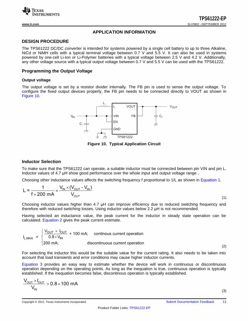
Output voltage
The output voltage is set by a resistor divider internally. The FB pin is used to sense the output voltage. Toconfigure the fixed output devices properly, the FB pin needs to be connected directly to VOUT as shown inFigure 10.
Figure 10. Typical Application Circuit
Inductor Selection
To make sure that the TPS61222 can operate, a suitable inductor must be connected between pin VIN and pin L.Inductor values of 4.7 μH show good performance over the whole input and output voltage range .
Choosing other inductance values affects the switching frequency f proportional to 1/L as shown in Equation 1.
(1)
Choosing inductor values higher than 4.7 μH can improve efficiency due to reduced switching frequency andtherefore with reduced switching losses. Using inductor values below 2.2 μH is not recommended.
Having selected an inductance value, the peak current for the inductor in steady state operation can becalculated. Equation 2 gives the peak current estimate.
(2)
For selecting the inductor this would be the suitable value for the current rating. It also needs to be taken intoaccount that load transients and error conditions may cause higher inductor currents.
Equation 3 provides an easy way to estimate whether the device will work in continuous or discontinuousoperation depending on the operating points. As long as the inequation is true, continuous operation is typicallyestablished. If the inequation becomes false, discontinous operation is typically established.
(3)
Copyright © 2012, Texas Instruments Incorporated Submit Documentation Feedback 11
Product Folder Links :TPS61222-EP
³ ´2
LC
2
TPS61222-EPSLVSBI2 –SEPTEMBER 2012 www.ti.com
The following inductor series from different suppliers have been used with TPS61222 converters:
Table 2. List of Inductors (1)
VENDOR INDUCTOR SERIES
EPL3015Coilcraft
EPL2010
Murata LQH3NP
Tajo Yuden NR3015
Wurth Elektronik WE-TPC Typ S
(1) Design was tested using these components at 25°C ambienttemperature.
Capacitor Selection
Input Capacitor
At least a 10-μF input capacitor is recommended to improve transient behavior of the regulator and EMI behaviorof the total power supply circuit. A ceramic capacitor placed as close as possible to the VIN and GND pins of theIC is recommended.
Output Capacitor
For the output capacitor C2 , it is recommended to use small ceramic capacitors placed as close as possible tothe VOUT and GND pins of the IC. If, for any reason, the application requires the use of large capacitors whichcan not be placed close to the IC, the use of a small ceramic capacitor with an capacitance value of around2.2μF in parallel to the large one is recommended. This small capacitor should be placed as close as possible tothe VOUT and GND pins of the IC.
A minimum capacitance value of 4.7 μF should be used, 10 μF are recommended. If the inductor value exceeds4.7 μH, the value of the output capacitance value needs to be half the inductance value or higher for stabilityreasons, see Equation 4.
(4)
The TPS61222 is not sensitive to the ESR in terms of stability. Using low ESR capacitors, such as ceramiccapacitors, is recommended anyway to minimize output voltage ripple. If heavy load changes are expected, theoutput capacitor value should be increased to avoid output voltage drops during fast load transients.
Layout Considerations
As for all switching power supplies, the layout is an important step in the design, especially at high peak currentsand high switching frequencies. If the layout is not carefully done, the regulator could show stability problems aswell as EMI problems. Therefore, use wide and short traces for the main current path and for the power groundpaths. The input and output capacitor, as well as the inductor should be placed as close as possible to the IC.
The feedback divider should be placed as close as possible to the control ground pin of the IC. To lay out theground, it is recommended to use short traces as well, separated from the power ground traces. This avoidsground shift problems, which can occur due to superimposition of power ground current and control groundcurrent. Assure that the ground traces are connected close to the device GND pin.
THERMAL INFORMATION
Implementation of integrated circuits in low-profile and fine-pitch surface-mount packages typically requiresspecial attention to power dissipation. Many system-dependent issues such as thermal coupling, airflow, addedheat sinks and convection surfaces, and the presence of other heat-generating components affect the power-dissipation limits of a given component.
12 Submit Documentation Feedback Copyright © 2012, Texas Instruments Incorporated
Product Folder Links :TPS61222-EP
TPS61222-EPwww.ti.com SLVSBI2 –SEPTEMBER 2012
Three basic approaches for enhancing thermal performance are listed below.• Improving the power-dissipation capability of the PCB design• Improving the thermal coupling of the component to the PCB• Introducing airflow in the system
For more details on how to use the thermal parameters in the dissipation ratings table please check the ThermalCharacteristics Application Note (SZZA017) and the IC Package Thermal Metrics Application Note (SPRA953).
Copyright © 2012, Texas Instruments Incorporated Submit Documentation Feedback 13
Product Folder Links :TPS61222-EP
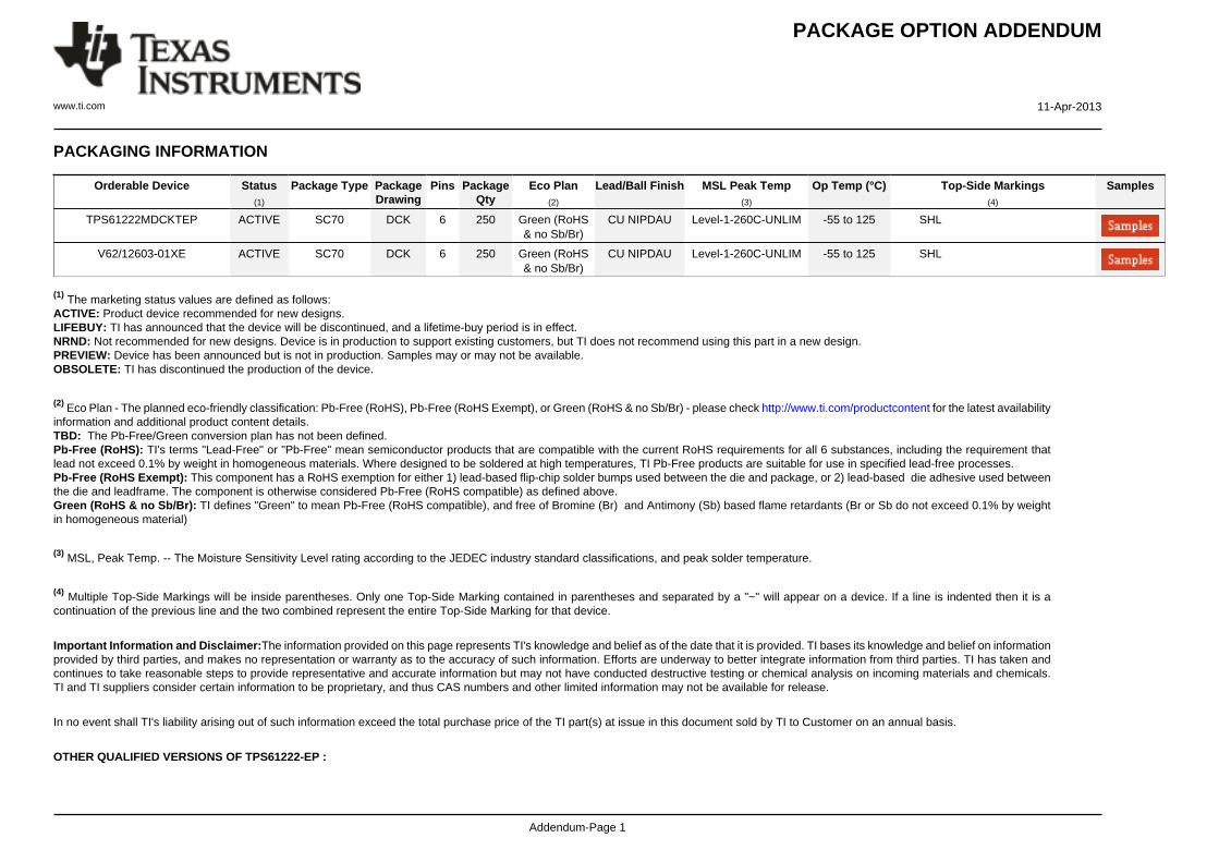
PACKAGE OPTION ADDENDUM
www.ti.com 11-Apr-2013
Addendum-Page 1
PACKAGING INFORMATION
Orderable Device Status(1)
Package Type PackageDrawing
Pins PackageQty
Eco Plan(2)
Lead/Ball Finish MSL Peak Temp(3)
Op Temp (°C) Top-Side Markings(4)
Samples
TPS61222MDCKTEP ACTIVE SC70 DCK 6 250 Green (RoHS& no Sb/Br)
CU NIPDAU Level-1-260C-UNLIM -55 to 125 SHL
V62/12603-01XE ACTIVE SC70 DCK 6 250 Green (RoHS& no Sb/Br)
CU NIPDAU Level-1-260C-UNLIM -55 to 125 SHL
(1) The marketing status values are defined as follows:ACTIVE: Product device recommended for new designs.LIFEBUY: TI has announced that the device will be discontinued, and a lifetime-buy period is in effect.NRND: Not recommended for new designs. Device is in production to support existing customers, but TI does not recommend using this part in a new design.PREVIEW: Device has been announced but is not in production. Samples may or may not be available.OBSOLETE: TI has discontinued the production of the device.
(2) Eco Plan - The planned eco-friendly classification: Pb-Free (RoHS), Pb-Free (RoHS Exempt), or Green (RoHS & no Sb/Br) - please check http://www.ti.com/productcontent for the latest availabilityinformation and additional product content details.TBD: The Pb-Free/Green conversion plan has not been defined.Pb-Free (RoHS): TI's terms "Lead-Free" or "Pb-Free" mean semiconductor products that are compatible with the current RoHS requirements for all 6 substances, including the requirement thatlead not exceed 0.1% by weight in homogeneous materials. Where designed to be soldered at high temperatures, TI Pb-Free products are suitable for use in specified lead-free processes.Pb-Free (RoHS Exempt): This component has a RoHS exemption for either 1) lead-based flip-chip solder bumps used between the die and package, or 2) lead-based die adhesive used betweenthe die and leadframe. The component is otherwise considered Pb-Free (RoHS compatible) as defined above.Green (RoHS & no Sb/Br): TI defines "Green" to mean Pb-Free (RoHS compatible), and free of Bromine (Br) and Antimony (Sb) based flame retardants (Br or Sb do not exceed 0.1% by weightin homogeneous material)
(3) MSL, Peak Temp. -- The Moisture Sensitivity Level rating according to the JEDEC industry standard classifications, and peak solder temperature.
(4) Multiple Top-Side Markings will be inside parentheses. Only one Top-Side Marking contained in parentheses and separated by a "~" will appear on a device. If a line is indented then it is acontinuation of the previous line and the two combined represent the entire Top-Side Marking for that device.
Important Information and Disclaimer:The information provided on this page represents TI's knowledge and belief as of the date that it is provided. TI bases its knowledge and belief on informationprovided by third parties, and makes no representation or warranty as to the accuracy of such information. Efforts are underway to better integrate information from third parties. TI has taken andcontinues to take reasonable steps to provide representative and accurate information but may not have conducted destructive testing or chemical analysis on incoming materials and chemicals.TI and TI suppliers consider certain information to be proprietary, and thus CAS numbers and other limited information may not be available for release.
In no event shall TI's liability arising out of such information exceed the total purchase price of the TI part(s) at issue in this document sold by TI to Customer on an annual basis.
OTHER QUALIFIED VERSIONS OF TPS61222-EP :
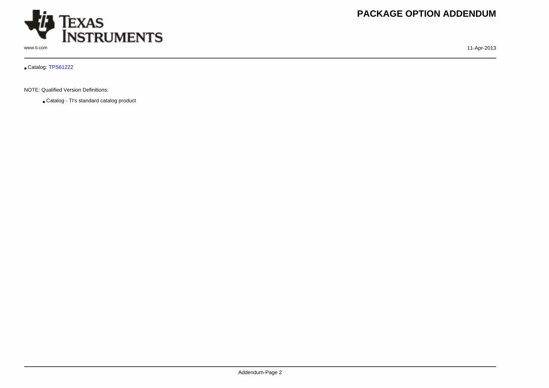
PACKAGE OPTION ADDENDUM
www.ti.com 11-Apr-2013
Addendum-Page 2
• Catalog: TPS61222
NOTE: Qualified Version Definitions:
• Catalog - TI's standard catalog product
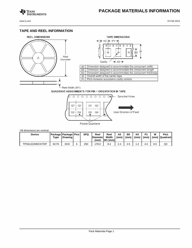
TAPE AND REEL INFORMATION
*All dimensions are nominal
Device PackageType
PackageDrawing
Pins SPQ ReelDiameter
(mm)
ReelWidth
W1 (mm)
A0(mm)
B0(mm)
K0(mm)
P1(mm)
W(mm)
Pin1Quadrant
TPS61222MDCKTEP SC70 DCK 6 250 178.0 8.4 2.4 2.5 1.2 4.0 8.0 Q3
PACKAGE MATERIALS INFORMATION
www.ti.com 15-Feb-2014
Pack Materials-Page 1
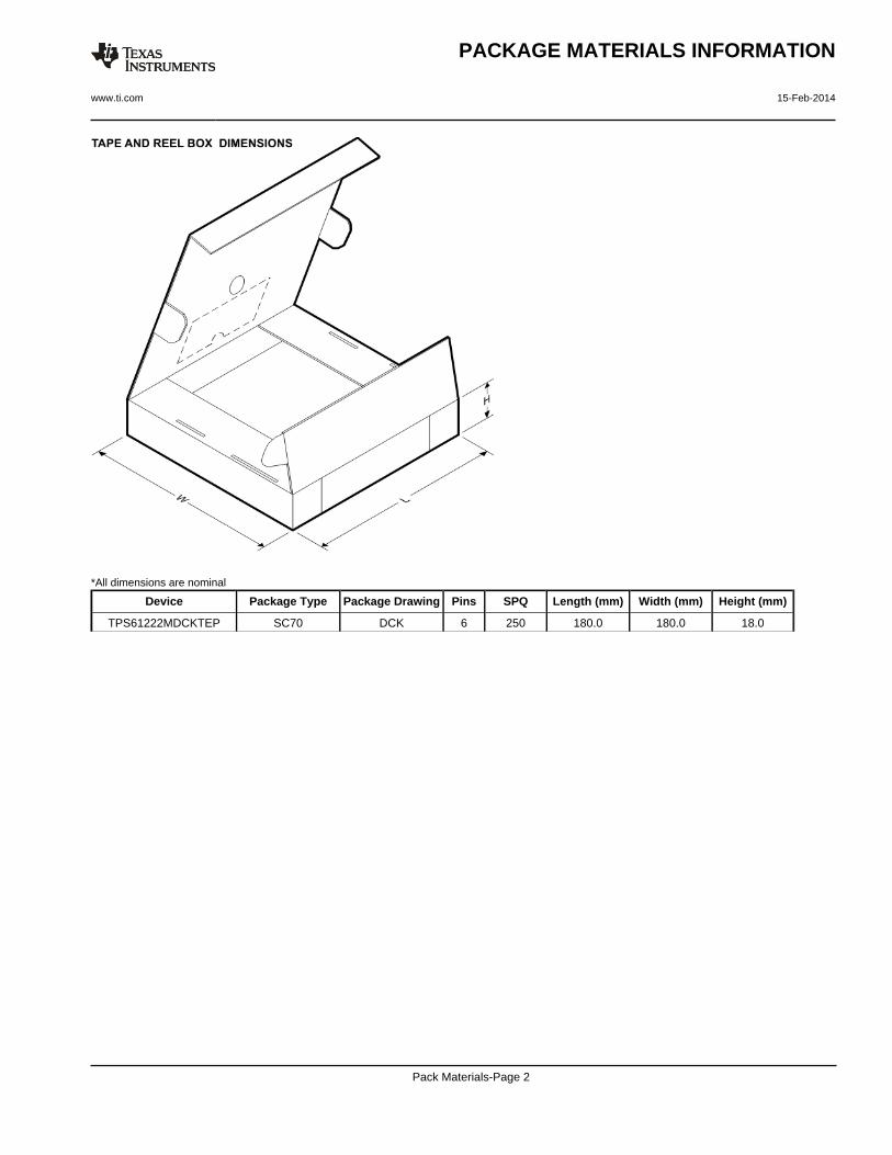
*All dimensions are nominal
Device Package Type Package Drawing Pins SPQ Length (mm) Width (mm) Height (mm)
TPS61222MDCKTEP SC70 DCK 6 250 180.0 180.0 18.0
PACKAGE MATERIALS INFORMATION
www.ti.com 15-Feb-2014
Pack Materials-Page 2
IMPORTANT NOTICE
Texas Instruments Incorporated and its subsidiaries (TI) reserve the right to make corrections, enhancements, improvements and otherchanges to its semiconductor products and services per JESD46, latest issue, and to discontinue any product or service per JESD48, latestissue. Buyers should obtain the latest relevant information before placing orders and should verify that such information is current andcomplete. All semiconductor products (also referred to herein as “components”) are sold subject to TI’s terms and conditions of salesupplied at the time of order acknowledgment.TI warrants performance of its components to the specifications applicable at the time of sale, in accordance with the warranty in TI’s termsand conditions of sale of semiconductor products. Testing and other quality control techniques are used to the extent TI deems necessaryto support this warranty. Except where mandated by applicable law, testing of all parameters of each component is not necessarilyperformed.TI assumes no liability for applications assistance or the design of Buyers’ products. Buyers are responsible for their products andapplications using TI components. To minimize the risks associated with Buyers’ products and applications, Buyers should provideadequate design and operating safeguards.TI does not warrant or represent that any license, either express or implied, is granted under any patent right, copyright, mask work right, orother intellectual property right relating to any combination, machine, or process in which TI components or services are used. Informationpublished by TI regarding third-party products or services does not constitute a license to use such products or services or a warranty orendorsement thereof. Use of such information may require a license from a third party under the patents or other intellectual property of thethird party, or a license from TI under the patents or other intellectual property of TI.Reproduction of significant portions of TI information in TI data books or data sheets is permissible only if reproduction is without alterationand is accompanied by all associated warranties, conditions, limitations, and notices. TI is not responsible or liable for such altereddocumentation. Information of third parties may be subject to additional restrictions.Resale of TI components or services with statements different from or beyond the parameters stated by TI for that component or servicevoids all express and any implied warranties for the associated TI component or service and is an unfair and deceptive business practice.TI is not responsible or liable for any such statements.Buyer acknowledges and agrees that it is solely responsible for compliance with all legal, regulatory and safety-related requirementsconcerning its products, and any use of TI components in its applications, notwithstanding any applications-related information or supportthat may be provided by TI. Buyer represents and agrees that it has all the necessary expertise to create and implement safeguards whichanticipate dangerous consequences of failures, monitor failures and their consequences, lessen the likelihood of failures that might causeharm and take appropriate remedial actions. Buyer will fully indemnify TI and its representatives against any damages arising out of the useof any TI components in safety-critical applications.In some cases, TI components may be promoted specifically to facilitate safety-related applications. With such components, TI’s goal is tohelp enable customers to design and create their own end-product solutions that meet applicable functional safety standards andrequirements. Nonetheless, such components are subject to these terms.No TI components are authorized for use in FDA Class III (or similar life-critical medical equipment) unless authorized officers of the partieshave executed a special agreement specifically governing such use.Only those TI components which TI has specifically designated as military grade or “enhanced plastic” are designed and intended for use inmilitary/aerospace applications or environments. Buyer acknowledges and agrees that any military or aerospace use of TI componentswhich have not been so designated is solely at the Buyer's risk, and that Buyer is solely responsible for compliance with all legal andregulatory requirements in connection with such use.TI has specifically designated certain components as meeting ISO/TS16949 requirements, mainly for automotive use. In any case of use ofnon-designated products, TI will not be responsible for any failure to meet ISO/TS16949.
Products ApplicationsAudio www.ti.com/audio Automotive and Transportation www.ti.com/automotiveAmplifiers amplifier.ti.com Communications and Telecom www.ti.com/communicationsData Converters dataconverter.ti.com Computers and Peripherals www.ti.com/computersDLP® Products www.dlp.com Consumer Electronics www.ti.com/consumer-appsDSP dsp.ti.com Energy and Lighting www.ti.com/energyClocks and Timers www.ti.com/clocks Industrial www.ti.com/industrialInterface interface.ti.com Medical www.ti.com/medicalLogic logic.ti.com Security www.ti.com/securityPower Mgmt power.ti.com Space, Avionics and Defense www.ti.com/space-avionics-defenseMicrocontrollers microcontroller.ti.com Video and Imaging www.ti.com/videoRFID www.ti-rfid.comOMAP Applications Processors www.ti.com/omap TI E2E Community e2e.ti.comWireless Connectivity www.ti.com/wirelessconnectivity
Mailing Address: Texas Instruments, Post Office Box 655303, Dallas, Texas 75265Copyright © 2016, Texas Instruments Incorporated