LMV721/LMV722 10MHz, Low Noise, Low Voltage, and • High Unity-Gain Bandwidth 10MHz The...
29
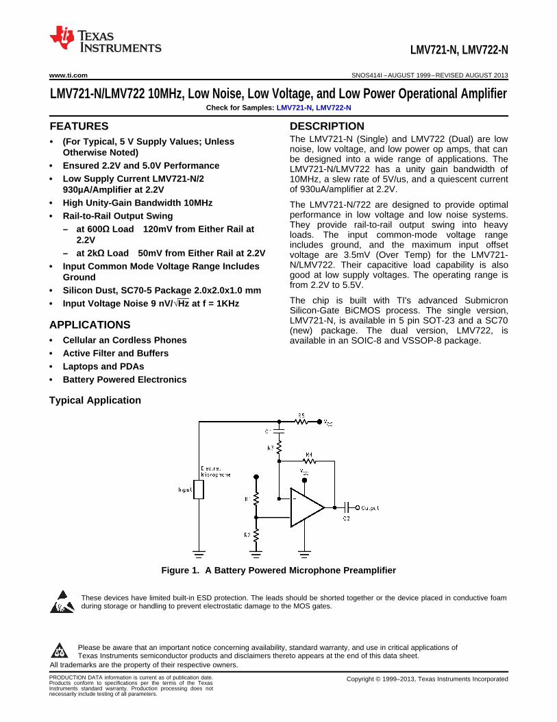
LMV721-N, LMV722-N www.ti.com SNOS414I – AUGUST 1999 – REVISED AUGUST 2013 LMV721-N/LMV722 10MHz, Low Noise, Low Voltage, and Low Power Operational Amplifier Check for Samples: LMV721-N, LMV722-N 1FEATURES DESCRIPTION The LMV721-N (Single) and LMV722 (Dual) are low 2• (For Typical, 5 V Supply Values; Unless noise, low voltage, and low power op amps, that can Otherwise Noted) be designed into a wide range of applications. The • Ensured 2.2V and 5.0V Performance LMV721-N/LMV722 has a unity gain bandwidth of • Low Supply Current LMV721-N/2 10MHz, a slew rate of 5V/us, and a quiescent current of 930uA/amplifier at 2.2V. 930μA/Amplifier at 2.2V • High Unity-Gain Bandwidth 10MHz The LMV721-N/722 are designed to provide optimal performance in low voltage and low noise systems. • Rail-to-Rail Output Swing They provide rail-to-rail output swing into heavy – at 600Ω Load 120mV from Either Rail at loads. The input common-mode voltage range 2.2V includes ground, and the maximum input offset – at 2kΩ Load 50mV from Either Rail at 2.2V voltage are 3.5mV (Over Temp) for the LMV721- N/LMV722. Their capacitive load capability is also • Input Common Mode Voltage Range Includes good at low supply voltages. The operating range is Ground from 2.2V to 5.5V. • Silicon Dust, SC70-5 Package 2.0x2.0x1.0 mm The chip is built with TI's advanced Submicron • Input Voltage Noise 9 nV/√Hz at f = 1KHz Silicon-Gate BiCMOS process. The single version, LMV721-N, is available in 5 pin SOT-23 and a SC70 APPLICATIONS (new) package. The dual version, LMV722, is • Cellular an Cordless Phones available in an SOIC-8 and VSSOP-8 package. • Active Filter and Buffers • Laptops and PDAs • Battery Powered Electronics Typical Application Figure 1. A Battery Powered Microphone Preamplifier These devices have limited built-in ESD protection. The leads should be shorted together or the device placed in conductive foam during storage or handling to prevent electrostatic damage to the MOS gates. 1 Please be aware that an important notice concerning availability, standard warranty, and use in critical applications of Texas Instruments semiconductor products and disclaimers thereto appears at the end of this data sheet. 2All trademarks are the property of their respective owners. PRODUCTION DATA information is current as of publication date. Copyright © 1999–2013, Texas Instruments Incorporated Products conform to specifications per the terms of the Texas Instruments standard warranty. Production processing does not necessarily include testing of all parameters.
Transcript of LMV721/LMV722 10MHz, Low Noise, Low Voltage, and • High Unity-Gain Bandwidth 10MHz The...
LMV721-N, LMV722-N
www.ti.com SNOS414I –AUGUST 1999–REVISED AUGUST 2013
LMV721-N/LMV722 10MHz, Low Noise, Low Voltage, and Low Power Operational AmplifierCheck for Samples: LMV721-N, LMV722-N
1FEATURES DESCRIPTIONThe LMV721-N (Single) and LMV722 (Dual) are low
2• (For Typical, 5 V Supply Values; Unlessnoise, low voltage, and low power op amps, that canOtherwise Noted)be designed into a wide range of applications. The
• Ensured 2.2V and 5.0V Performance LMV721-N/LMV722 has a unity gain bandwidth of• Low Supply Current LMV721-N/2 10MHz, a slew rate of 5V/us, and a quiescent current
of 930uA/amplifier at 2.2V.930µA/Amplifier at 2.2V• High Unity-Gain Bandwidth 10MHz The LMV721-N/722 are designed to provide optimal
performance in low voltage and low noise systems.• Rail-to-Rail Output SwingThey provide rail-to-rail output swing into heavy– at 600Ω Load 120mV from Either Rail at loads. The input common-mode voltage range2.2V includes ground, and the maximum input offset
– at 2kΩ Load 50mV from Either Rail at 2.2V voltage are 3.5mV (Over Temp) for the LMV721-N/LMV722. Their capacitive load capability is also• Input Common Mode Voltage Range Includesgood at low supply voltages. The operating range isGroundfrom 2.2V to 5.5V.• Silicon Dust, SC70-5 Package 2.0x2.0x1.0 mmThe chip is built with TI's advanced Submicron• Input Voltage Noise 9 nV/√Hz at f = 1KHzSilicon-Gate BiCMOS process. The single version,LMV721-N, is available in 5 pin SOT-23 and a SC70APPLICATIONS (new) package. The dual version, LMV722, is
• Cellular an Cordless Phones available in an SOIC-8 and VSSOP-8 package.• Active Filter and Buffers• Laptops and PDAs• Battery Powered Electronics
Typical Application
Figure 1. A Battery Powered Microphone Preamplifier
These devices have limited built-in ESD protection. The leads should be shorted together or the device placed in conductive foamduring storage or handling to prevent electrostatic damage to the MOS gates.
1
Please be aware that an important notice concerning availability, standard warranty, and use in critical applications ofTexas Instruments semiconductor products and disclaimers thereto appears at the end of this data sheet.
2All trademarks are the property of their respective owners.PRODUCTION DATA information is current as of publication date. Copyright © 1999–2013, Texas Instruments IncorporatedProducts conform to specifications per the terms of the TexasInstruments standard warranty. Production processing does notnecessarily include testing of all parameters.
LMV721-N, LMV722-N
SNOS414I –AUGUST 1999–REVISED AUGUST 2013 www.ti.com
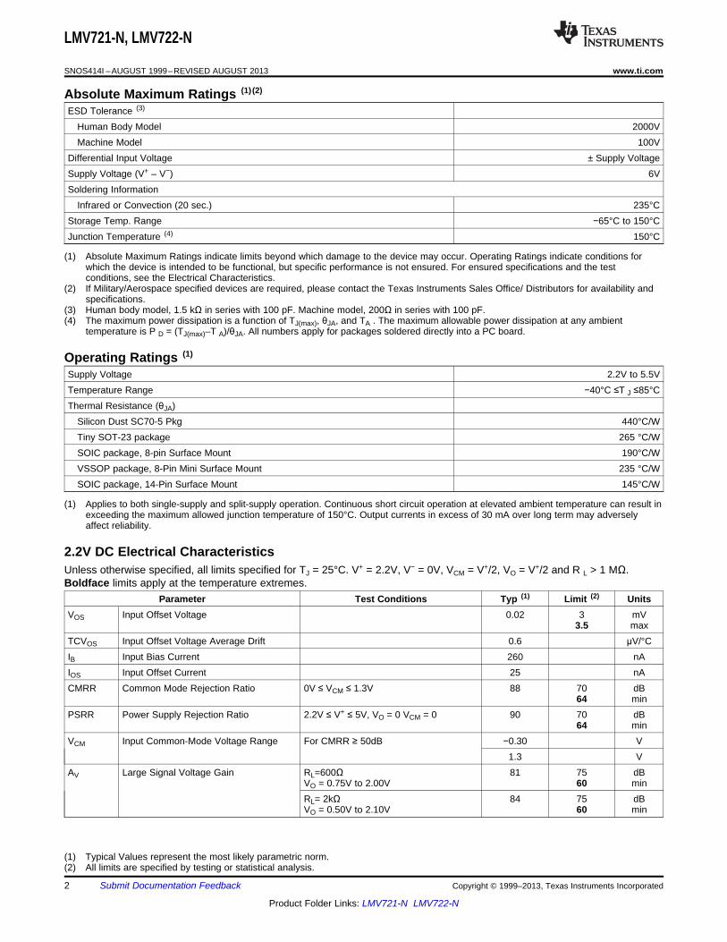
Absolute Maximum Ratings (1) (2)
ESD Tolerance (3)
Human Body Model 2000VMachine Model 100V
Differential Input Voltage ± Supply VoltageSupply Voltage (V+ – V−) 6VSoldering Information
Infrared or Convection (20 sec.) 235°CStorage Temp. Range −65°C to 150°CJunction Temperature (4) 150°C
(1) Absolute Maximum Ratings indicate limits beyond which damage to the device may occur. Operating Ratings indicate conditions forwhich the device is intended to be functional, but specific performance is not ensured. For ensured specifications and the testconditions, see the Electrical Characteristics.
(2) If Military/Aerospace specified devices are required, please contact the Texas Instruments Sales Office/ Distributors for availability andspecifications.
(3) Human body model, 1.5 kΩ in series with 100 pF. Machine model, 200Ω in series with 100 pF.(4) The maximum power dissipation is a function of TJ(max), θJA, and TA . The maximum allowable power dissipation at any ambient
temperature is P D = (TJ(max)–T A)/θJA. All numbers apply for packages soldered directly into a PC board.
Operating Ratings (1)
Supply Voltage 2.2V to 5.5VTemperature Range −40°C ≤T J ≤85°CThermal Resistance (θJA)
Silicon Dust SC70-5 Pkg 440°C/WTiny SOT-23 package 265 °C/WSOIC package, 8-pin Surface Mount 190°C/WVSSOP package, 8-Pin Mini Surface Mount 235 °C/WSOIC package, 14-Pin Surface Mount 145°C/W
(1) Applies to both single-supply and split-supply operation. Continuous short circuit operation at elevated ambient temperature can result inexceeding the maximum allowed junction temperature of 150°C. Output currents in excess of 30 mA over long term may adverselyaffect reliability.
2.2V DC Electrical CharacteristicsUnless otherwise specified, all limits specified for TJ = 25°C. V+ = 2.2V, V− = 0V, VCM = V+/2, VO = V+/2 and R L > 1 MΩ.Boldface limits apply at the temperature extremes.
Parameter Test Conditions Typ (1) Limit (2) UnitsVOS Input Offset Voltage 0.02 3 mV
3.5 maxTCVOS Input Offset Voltage Average Drift 0.6 μV/°CIB Input Bias Current 260 nAIOS Input Offset Current 25 nACMRR Common Mode Rejection Ratio 0V ≤ VCM ≤ 1.3V 88 70 dB
64 minPSRR Power Supply Rejection Ratio 2.2V ≤ V+ ≤ 5V, VO = 0 VCM = 0 90 70 dB
64 minVCM Input Common-Mode Voltage Range For CMRR ≥ 50dB −0.30 V
1.3 VAV Large Signal Voltage Gain RL=600Ω 81 75 dB
VO = 0.75V to 2.00V 60 minRL= 2kΩ 84 75 dBVO = 0.50V to 2.10V 60 min
(1) Typical Values represent the most likely parametric norm.(2) All limits are specified by testing or statistical analysis.
2 Submit Documentation Feedback Copyright © 1999–2013, Texas Instruments Incorporated
Product Folder Links: LMV721-N LMV722-N
LMV721-N, LMV722-N
www.ti.com SNOS414I –AUGUST 1999–REVISED AUGUST 2013
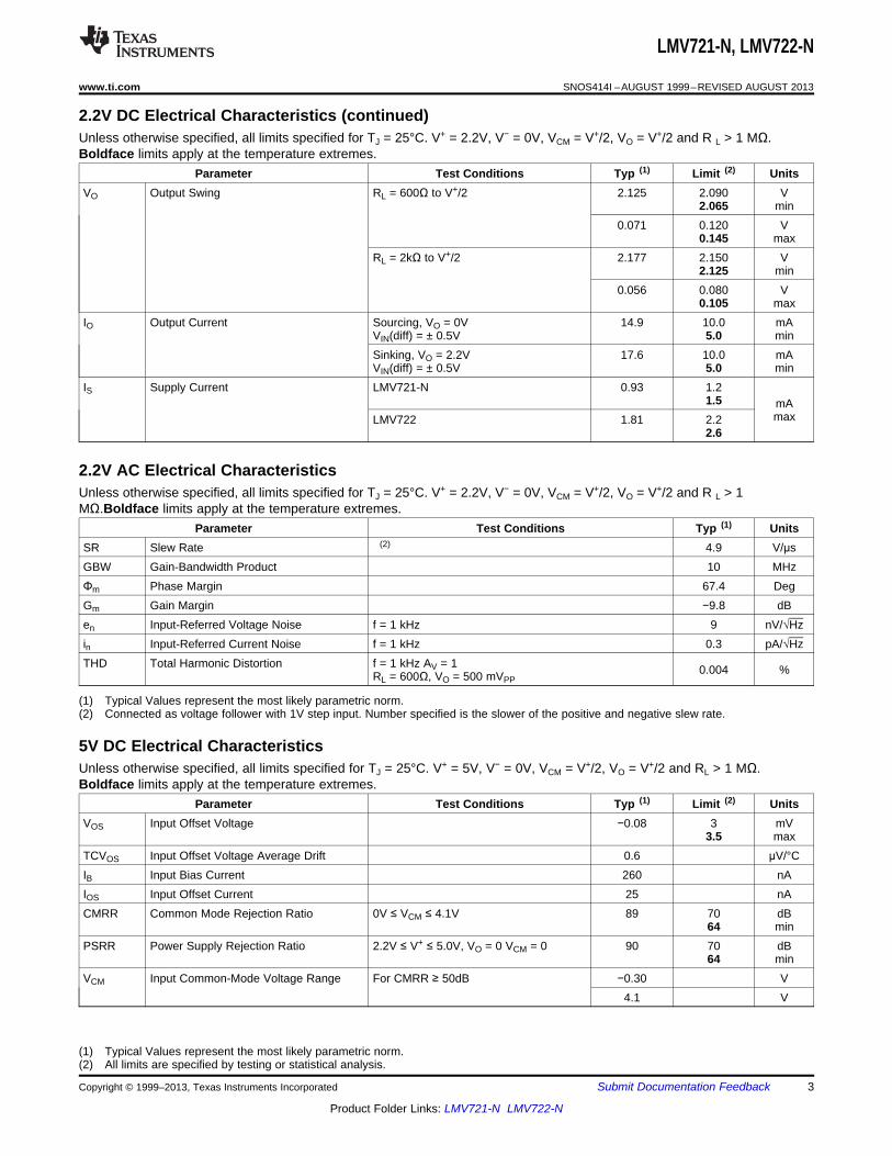
2.2V DC Electrical Characteristics (continued)Unless otherwise specified, all limits specified for TJ = 25°C. V+ = 2.2V, V− = 0V, VCM = V+/2, VO = V+/2 and R L > 1 MΩ.Boldface limits apply at the temperature extremes.
Parameter Test Conditions Typ (1) Limit (2) UnitsVO Output Swing RL = 600Ω to V+/2 2.125 2.090 V
2.065 min0.071 0.120 V
0.145 maxRL = 2kΩ to V+/2 2.177 2.150 V
2.125 min0.056 0.080 V
0.105 maxIO Output Current Sourcing, VO = 0V 14.9 10.0 mA
VIN(diff) = ± 0.5V 5.0 minSinking, VO = 2.2V 17.6 10.0 mAVIN(diff) = ± 0.5V 5.0 min
IS Supply Current LMV721-N 0.93 1.21.5 mA
maxLMV722 1.81 2.22.6
2.2V AC Electrical CharacteristicsUnless otherwise specified, all limits specified for TJ = 25°C. V+ = 2.2V, V− = 0V, VCM = V+/2, VO = V+/2 and R L > 1MΩ.Boldface limits apply at the temperature extremes.
Parameter Test Conditions Typ (1) UnitsSR Slew Rate (2) 4.9 V/μsGBW Gain-Bandwidth Product 10 MHzΦm Phase Margin 67.4 DegGm Gain Margin −9.8 dBen Input-Referred Voltage Noise f = 1 kHz 9 nV/√Hzin Input-Referred Current Noise f = 1 kHz 0.3 pA/√HzTHD Total Harmonic Distortion f = 1 kHz AV = 1 0.004 %RL = 600Ω, VO = 500 mVPP
(1) Typical Values represent the most likely parametric norm.(2) Connected as voltage follower with 1V step input. Number specified is the slower of the positive and negative slew rate.
5V DC Electrical CharacteristicsUnless otherwise specified, all limits specified for TJ = 25°C. V+ = 5V, V− = 0V, VCM = V+/2, VO = V+/2 and RL > 1 MΩ.Boldface limits apply at the temperature extremes.
Parameter Test Conditions Typ (1) Limit (2) UnitsVOS Input Offset Voltage −0.08 3 mV
3.5 maxTCVOS Input Offset Voltage Average Drift 0.6 μV/°CIB Input Bias Current 260 nAIOS Input Offset Current 25 nACMRR Common Mode Rejection Ratio 0V ≤ VCM ≤ 4.1V 89 70 dB
64 minPSRR Power Supply Rejection Ratio 2.2V ≤ V+ ≤ 5.0V, VO = 0 VCM = 0 90 70 dB
64 minVCM Input Common-Mode Voltage Range For CMRR ≥ 50dB −0.30 V
4.1 V
(1) Typical Values represent the most likely parametric norm.(2) All limits are specified by testing or statistical analysis.
Copyright © 1999–2013, Texas Instruments Incorporated Submit Documentation Feedback 3
Product Folder Links: LMV721-N LMV722-N
LMV721-N, LMV722-N
SNOS414I –AUGUST 1999–REVISED AUGUST 2013 www.ti.com
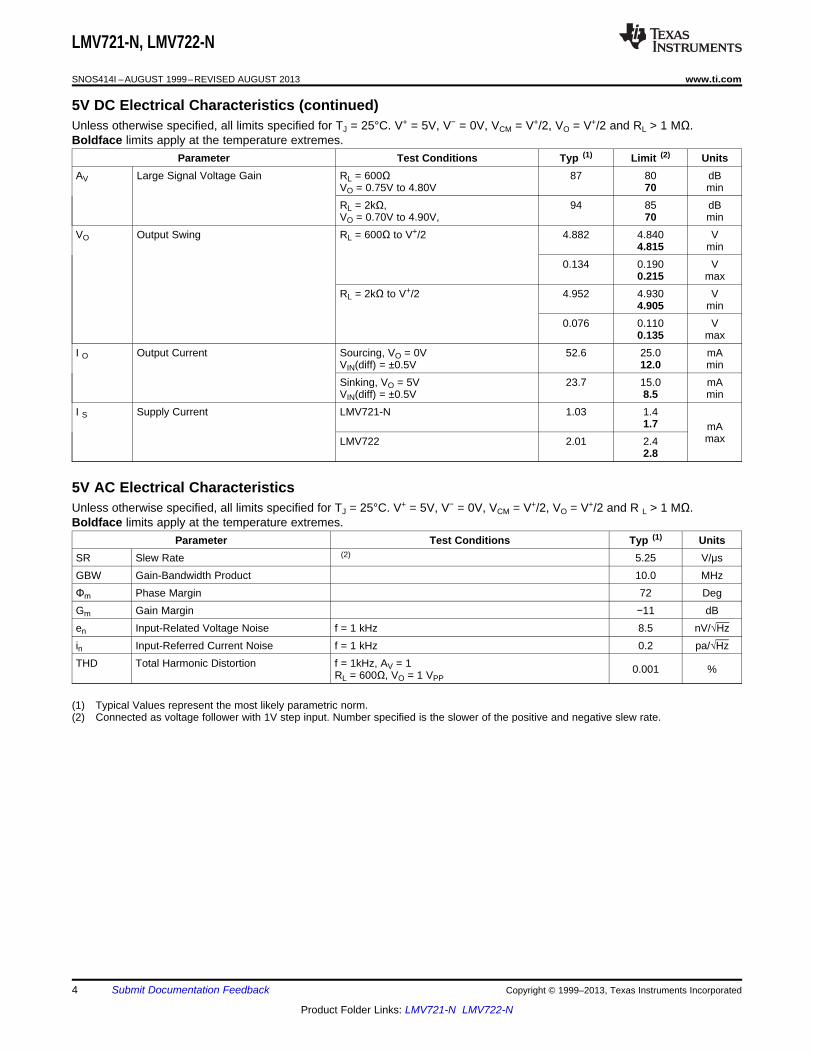
5V DC Electrical Characteristics (continued)Unless otherwise specified, all limits specified for TJ = 25°C. V+ = 5V, V− = 0V, VCM = V+/2, VO = V+/2 and RL > 1 MΩ.Boldface limits apply at the temperature extremes.
Parameter Test Conditions Typ (1) Limit (2) UnitsAV Large Signal Voltage Gain RL = 600Ω 87 80 dB
VO = 0.75V to 4.80V 70 minRL = 2kΩ, 94 85 dBVO = 0.70V to 4.90V, 70 min
VO Output Swing RL = 600Ω to V+/2 4.882 4.840 V4.815 min
0.134 0.190 V0.215 max
RL = 2kΩ to V+/2 4.952 4.930 V4.905 min
0.076 0.110 V0.135 max
I O Output Current Sourcing, VO = 0V 52.6 25.0 mAVIN(diff) = ±0.5V 12.0 minSinking, VO = 5V 23.7 15.0 mAVIN(diff) = ±0.5V 8.5 min
I S Supply Current LMV721-N 1.03 1.41.7 mA
maxLMV722 2.01 2.42.8
5V AC Electrical CharacteristicsUnless otherwise specified, all limits specified for TJ = 25°C. V+ = 5V, V− = 0V, VCM = V+/2, VO = V+/2 and R L > 1 MΩ.Boldface limits apply at the temperature extremes.
Parameter Test Conditions Typ (1) UnitsSR Slew Rate (2) 5.25 V/μsGBW Gain-Bandwidth Product 10.0 MHzΦm Phase Margin 72 DegGm Gain Margin −11 dBen Input-Related Voltage Noise f = 1 kHz 8.5 nV/√Hzin Input-Referred Current Noise f = 1 kHz 0.2 pa/√HzTHD Total Harmonic Distortion f = 1kHz, AV = 1 0.001 %RL = 600Ω, VO = 1 VPP
(1) Typical Values represent the most likely parametric norm.(2) Connected as voltage follower with 1V step input. Number specified is the slower of the positive and negative slew rate.
4 Submit Documentation Feedback Copyright © 1999–2013, Texas Instruments Incorporated
Product Folder Links: LMV721-N LMV722-N
LMV721-N, LMV722-N
www.ti.com SNOS414I –AUGUST 1999–REVISED AUGUST 2013
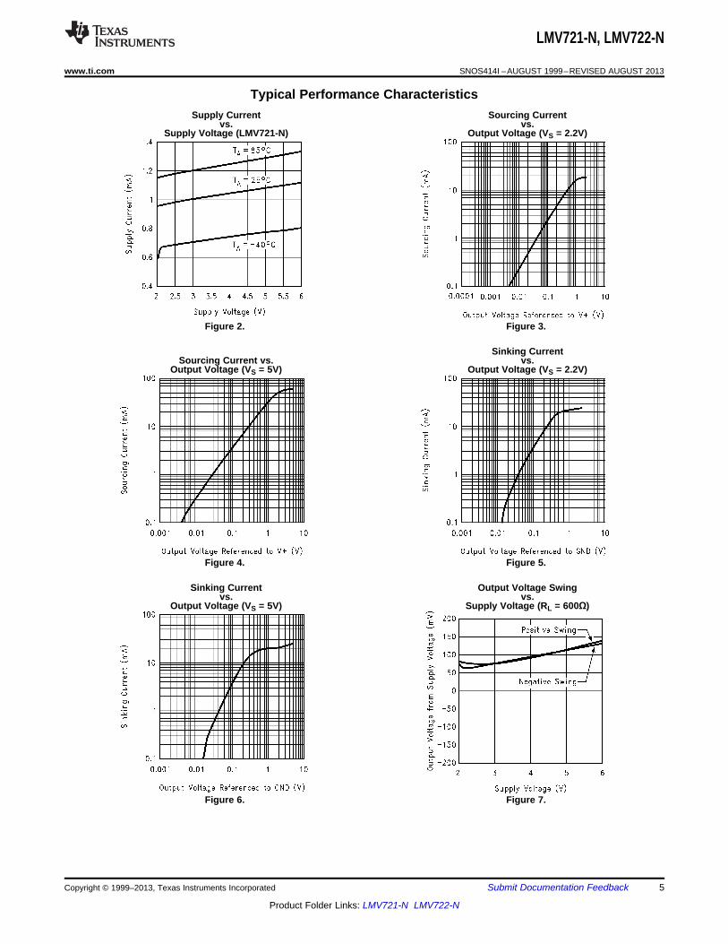
Typical Performance CharacteristicsSupply Current Sourcing Current
vs. vs.Supply Voltage (LMV721-N) Output Voltage (VS = 2.2V)
Figure 2. Figure 3.
Sinking CurrentSourcing Current vs. vs.
Output Voltage (VS = 5V) Output Voltage (VS = 2.2V)
Figure 4. Figure 5.
Sinking Current Output Voltage Swingvs. vs.
Output Voltage (VS = 5V) Supply Voltage (RL = 600Ω)
Figure 6. Figure 7.
Copyright © 1999–2013, Texas Instruments Incorporated Submit Documentation Feedback 5
Product Folder Links: LMV721-N LMV722-N
LMV721-N, LMV722-N
SNOS414I –AUGUST 1999–REVISED AUGUST 2013 www.ti.com
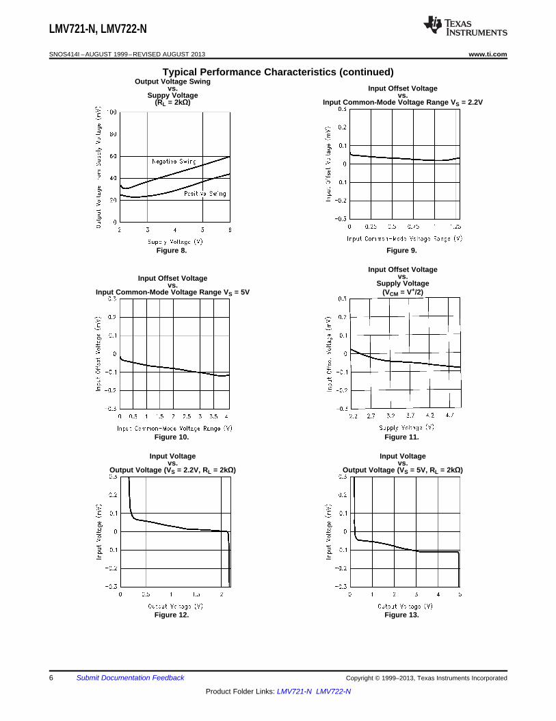
Typical Performance Characteristics (continued)Output Voltage Swing
vs. Input Offset VoltageSuppy Voltage vs.
(RL = 2kΩ) Input Common-Mode Voltage Range VS = 2.2V
Figure 8. Figure 9.
Input Offset Voltagevs.Input Offset Voltage
Supply Voltagevs.Input Common-Mode Voltage Range VS = 5V (VCM = V+/2)
Figure 10. Figure 11.
Input Voltage Input Voltagevs. vs.
Output Voltage (VS = 2.2V, RL = 2kΩ) Output Voltage (VS = 5V, RL = 2kΩ)
Figure 12. Figure 13.
6 Submit Documentation Feedback Copyright © 1999–2013, Texas Instruments Incorporated
Product Folder Links: LMV721-N LMV722-N
LMV721-N, LMV722-N
www.ti.com SNOS414I –AUGUST 1999–REVISED AUGUST 2013
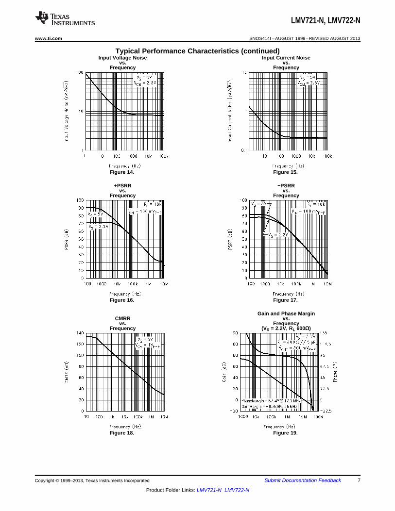
Typical Performance Characteristics (continued)Input Voltage Noise Input Current Noise
vs. vs.Frequency Frequency
Figure 14. Figure 15.
+PSRR −PSRRvs. vs.
Frequency Frequency
Figure 16. Figure 17.
Gain and Phase MarginCMRR vs.
vs. FrequencyFrequency (VS = 2.2V, RL 600Ω)
Figure 18. Figure 19.
Copyright © 1999–2013, Texas Instruments Incorporated Submit Documentation Feedback 7
Product Folder Links: LMV721-N LMV722-N

LMV721-N, LMV722-N
SNOS414I –AUGUST 1999–REVISED AUGUST 2013 www.ti.com
Typical Performance Characteristics (continued)Gain and Phase Margin
vs. Slew RateFrequency vs.
(VS = 5V, RL 600Ω) Supply Voltage
Figure 20. Figure 21.
THDvs.
Frequency
Figure 22.
8 Submit Documentation Feedback Copyright © 1999–2013, Texas Instruments Incorporated
Product Folder Links: LMV721-N LMV722-N
LMV721-N, LMV722-N
www.ti.com SNOS414I –AUGUST 1999–REVISED AUGUST 2013
APPLICATION NOTES
BENEFITS OF THE LMV721-N/722 SIZEThe small footprints of the LMV721-N/722 packages save space on printed circuit boards, and enable the designof smaller electronic products, such as cellular phones, pagers, or other portable systems. The low profile of theLMV721-N/722 make them possible to use in PCMCIA type III cards.
Signal Integrity Signals can pick up noise between the signal source and the amplifier. By using a physicallysmaller amplifier package, the LMV721-N/722 can be placed closer to the signal source, reducing noisepickup and increasing signal integrity.
Simplified Board Layout These products help you to avoid using long pc traces in your pc board layout. Thismeans that no additional components, such as capacitors and resistors, are needed to filter out theunwanted signals due to the interference between the long pc traces.
Low Supply CurrentThese devices will help you to maximize battery life. They are ideal for battery poweredsystems.
Low Supply Voltage TI provides ensured performance at 2.2V and 5V. These specifications ensure operationthroughout the battery lifetime.
Rail-to-Rail Output Rail-to-rail output swing provides maximum possible dynamic range at the output. This isparticularly important when operating on low supply voltages.
Input Includes Ground Allows direct sensing near GND in single supply operation.
Protection should be provided to prevent the input voltages from going negative more than −0.3V (at 25°C). Aninput clamp diode with a resistor to the IC input terminal can be used.
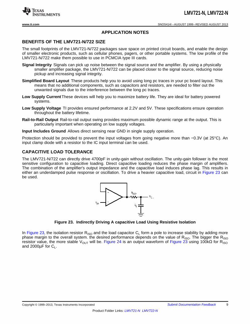
CAPACITIVE LOAD TOLERANCEThe LMV721-N/722 can directly drive 4700pF in unity-gain without oscillation. The unity-gain follower is the mostsensitive configuration to capacitive loading. Direct capacitive loading reduces the phase margin of amplifiers.The combination of the amplifier's output impedance and the capacitive load induces phase lag. This results ineither an underdamped pulse response or oscillation. To drive a heavier capacitive load, circuit in Figure 23 canbe used.
Figure 23. Indirectly Driving A capacitive Load Using Resistive Isolation
In Figure 23, the isolation resistor RISO and the load capacitor CL form a pole to increase stability by adding morephase margin to the overall system. the desired performance depends on the value of RISO. The bigger the RISOresistor value, the more stable VOUT will be. Figure 24 is an output waveform of Figure 23 using 100kΩ for RISOand 2000µF for CL.
Copyright © 1999–2013, Texas Instruments Incorporated Submit Documentation Feedback 9
Product Folder Links: LMV721-N LMV722-N
LMV721-N, LMV722-N
SNOS414I –AUGUST 1999–REVISED AUGUST 2013 www.ti.com
Figure 24. Pulse Response of the LMV721-N Circuit in Figure 23
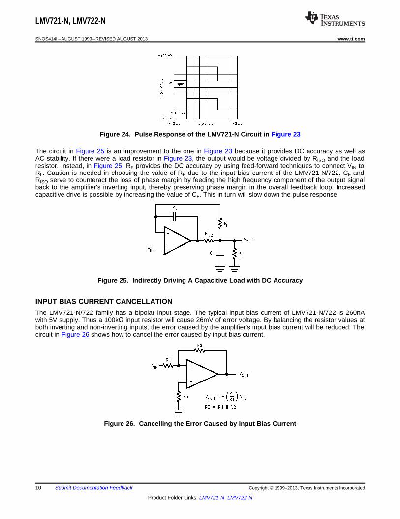
The circuit in Figure 25 is an improvement to the one in Figure 23 because it provides DC accuracy as well asAC stability. If there were a load resistor in Figure 23, the output would be voltage divided by RISO and the loadresistor. Instead, in Figure 25, RF provides the DC accuracy by using feed-forward techniques to connect VIN toRL. Caution is needed in choosing the value of RF due to the input bias current of the LMV721-N/722. CF andRISO serve to counteract the loss of phase margin by feeding the high frequency component of the output signalback to the amplifier's inverting input, thereby preserving phase margin in the overall feedback loop. Increasedcapacitive drive is possible by increasing the value of CF. This in turn will slow down the pulse response.
Figure 25. Indirectly Driving A Capacitive Load with DC Accuracy
INPUT BIAS CURRENT CANCELLATIONThe LMV721-N/722 family has a bipolar input stage. The typical input bias current of LMV721-N/722 is 260nAwith 5V supply. Thus a 100kΩ input resistor will cause 26mV of error voltage. By balancing the resistor values atboth inverting and non-inverting inputs, the error caused by the amplifier's input bias current will be reduced. Thecircuit in Figure 26 shows how to cancel the error caused by input bias current.
Figure 26. Cancelling the Error Caused by Input Bias Current
10 Submit Documentation Feedback Copyright © 1999–2013, Texas Instruments Incorporated
Product Folder Links: LMV721-N LMV722-N

LMV721-N, LMV722-N
www.ti.com SNOS414I –AUGUST 1999–REVISED AUGUST 2013
TYPICAL SINGLE-SUPPLY APPLICATION CIRCUITS
Difference AmplifierThe difference amplifier allows the subtraction of two voltages or, as a special case, the cancellation of a signalcommon to two inputs. It is useful as a computational amplifier, in making a differential to single-endedconversion or in rejecting a common mode signal.
Figure 27. Difference Application
(1)
(2)
Instrumentation CircuitsThe input impendance of the previous difference amplifier is set by the resistor R1, R2, R3 and R4. To eliminatethe problems of low input impendance, one way is to use a voltage follower ahead of each input as shown in thefollowing two instrumentation amplifiers.
Three-op-amp Instrumentation AmplifierThe LMV721-N/722 can be used to build a three-op-amp instrumentation amplifier as shown in Figure 28
Figure 28. Three-op-amp Instrumentation Amplifier
The first stage of this instrumentation amplifier is a differential-input, differential-output amplifier, with two voltagefollowers. These two voltage followers assure that the input impedance is over 100MΩ. The gain of thisinstrumentation amplifier is set by the ratio of R2/R1. R3 should equal R1 and R4 equal R2. Matching of R3 to R1and R4 to R2 affects the CMRR. For good CMRR over temperature, low drift resistors should be used. Making R4slightly smaller than R2 and adding a trim pot equal to twice the difference between R2 and R4 will allow theCMRR to be adjusted for optimum.
Copyright © 1999–2013, Texas Instruments Incorporated Submit Documentation Feedback 11
Product Folder Links: LMV721-N LMV722-N
LMV721-N, LMV722-N
SNOS414I –AUGUST 1999–REVISED AUGUST 2013 www.ti.com
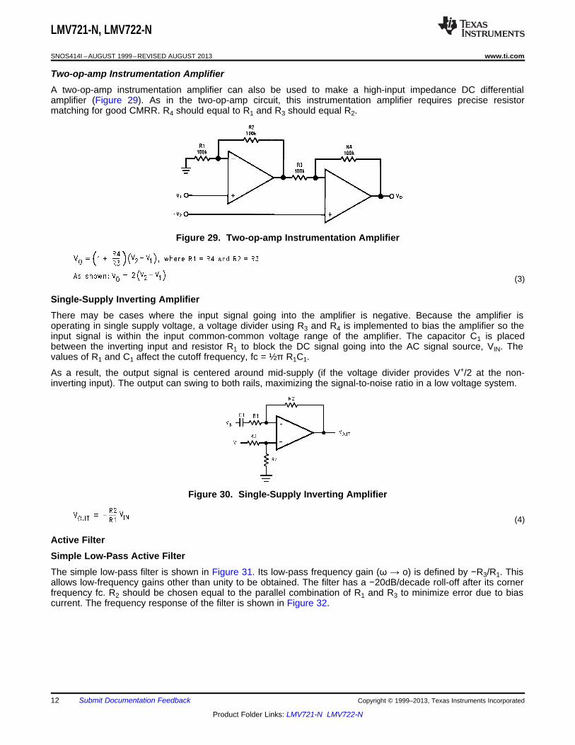
Two-op-amp Instrumentation AmplifierA two-op-amp instrumentation amplifier can also be used to make a high-input impedance DC differentialamplifier (Figure 29). As in the two-op-amp circuit, this instrumentation amplifier requires precise resistormatching for good CMRR. R4 should equal to R1 and R3 should equal R2.
Figure 29. Two-op-amp Instrumentation Amplifier
(3)
Single-Supply Inverting AmplifierThere may be cases where the input signal going into the amplifier is negative. Because the amplifier isoperating in single supply voltage, a voltage divider using R3 and R4 is implemented to bias the amplifier so theinput signal is within the input common-common voltage range of the amplifier. The capacitor C1 is placedbetween the inverting input and resistor R1 to block the DC signal going into the AC signal source, VIN. Thevalues of R1 and C1 affect the cutoff frequency, fc = ½π R1C1.
As a result, the output signal is centered around mid-supply (if the voltage divider provides V+/2 at the non-inverting input). The output can swing to both rails, maximizing the signal-to-noise ratio in a low voltage system.
Figure 30. Single-Supply Inverting Amplifier
(4)
Active FilterSimple Low-Pass Active FilterThe simple low-pass filter is shown in Figure 31. Its low-pass frequency gain (ω → o) is defined by −R3/R1. Thisallows low-frequency gains other than unity to be obtained. The filter has a −20dB/decade roll-off after its cornerfrequency fc. R2 should be chosen equal to the parallel combination of R1 and R3 to minimize error due to biascurrent. The frequency response of the filter is shown in Figure 32.
12 Submit Documentation Feedback Copyright © 1999–2013, Texas Instruments Incorporated
Product Folder Links: LMV721-N LMV722-N
LMV721-N, LMV722-N
www.ti.com SNOS414I –AUGUST 1999–REVISED AUGUST 2013
Figure 31. Simple Low-Pass Active Filter
(5)
Figure 32. Frequency Response of Simple Low-pass Active Filter in Figure 31
Note that the single-op-amp active filters are used in to the applications that require low quality factor, Q(≤ 10),low frequency (≤ 5KHz), and low gain (≤ 10), or a small value for the product of gain times Q(≤ 100). The op ampshould have an open loop voltage gain at the highest frequency of interest at least 50 times larger than the gainof the filter at this frequency. In addition, the selected op amp should have a slew rate that meets the followingrequirement:Slew Rate ≥ 0.5 x (ωH VOPP) X 10 −6V/µsec
where• ωH is the highest frequency of interest• VOPP is the output peak-to-peak voltage
Figure 33. A Battery Powered Microphone Preamplifier
Copyright © 1999–2013, Texas Instruments Incorporated Submit Documentation Feedback 13
Product Folder Links: LMV721-N LMV722-N

LMV721-N, LMV722-N
SNOS414I –AUGUST 1999–REVISED AUGUST 2013 www.ti.com
Here is a LMV721-N used as a microphone preamplifier. Since the LMV721-N is a low noise and low power opamp, it makes it an ideal candidate as a battery powered microphone preamplifier. The LMV721-N is connectedin an inverting configuration. Resistors, R1 = R2 = 4.7kΩ, sets the reference half way between VCC = 3V andground. Thus, this configures the op amp for single supply use. The gain of the preamplifier, which is 50 (34dB),is set by resistors R3 = 10kΩ and R4 = 500kΩ. The gain bandwidth product for the LMV721-N is 10 MHz. This issufficient for most audio application since the audio range is typically from 20 Hz to 20kHz. A resistor R5 = 5kΩ isused to bias the electret microphone. Capacitors C1 = C2 = 4.7µF placed at the input and output of the op amp toblock out the DC voltage offset.
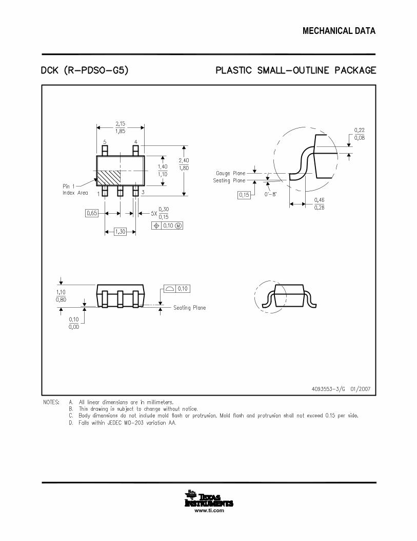
Connection Diagrams
Top View Top View
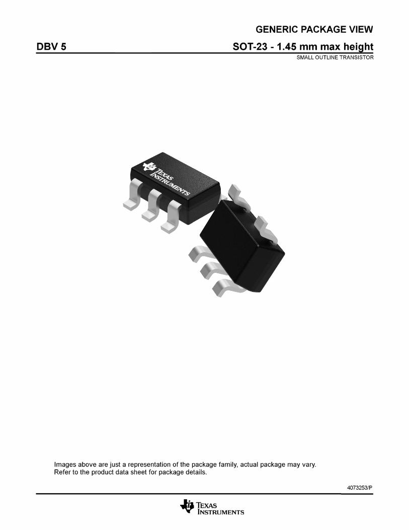
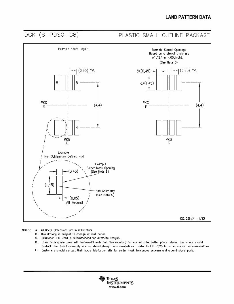
Figure 34. 5-Pin SC70 and SOT-23 Packages Figure 35. 8-Pin SOIC and VSSOP PackagesSee Package Numbers DCK0005A AND DBV0005A See Package Numbers D0008A and DGK0008A
14 Submit Documentation Feedback Copyright © 1999–2013, Texas Instruments Incorporated
Product Folder Links: LMV721-N LMV722-N
LMV721-N, LMV722-N
www.ti.com SNOS414I –AUGUST 1999–REVISED AUGUST 2013
REVISION HISTORY
Changes from Revision G (March 2013) to Revision H Page
• Changed layout of National Data Sheet to TI format .......................................................................................................... 14
Copyright © 1999–2013, Texas Instruments Incorporated Submit Documentation Feedback 15
Product Folder Links: LMV721-N LMV722-N
PACKAGE OPTION ADDENDUM
www.ti.com 17-Mar-2017
Addendum-Page 1
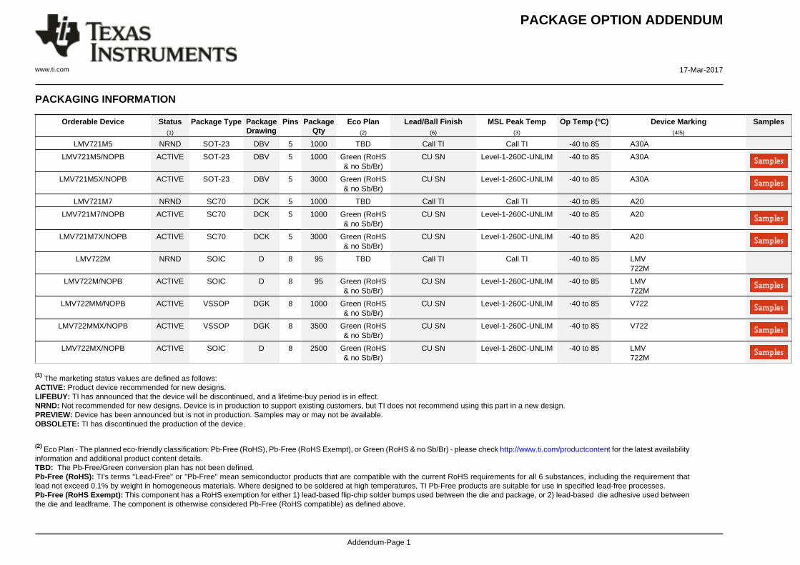
PACKAGING INFORMATION
Orderable Device Status(1)
Package Type PackageDrawing
Pins PackageQty
Eco Plan(2)
Lead/Ball Finish(6)
MSL Peak Temp(3)
Op Temp (°C) Device Marking(4/5)
Samples
LMV721M5 NRND SOT-23 DBV 5 1000 TBD Call TI Call TI -40 to 85 A30A
LMV721M5/NOPB ACTIVE SOT-23 DBV 5 1000 Green (RoHS& no Sb/Br)
CU SN Level-1-260C-UNLIM -40 to 85 A30A
LMV721M5X/NOPB ACTIVE SOT-23 DBV 5 3000 Green (RoHS& no Sb/Br)
CU SN Level-1-260C-UNLIM -40 to 85 A30A
LMV721M7 NRND SC70 DCK 5 1000 TBD Call TI Call TI -40 to 85 A20
LMV721M7/NOPB ACTIVE SC70 DCK 5 1000 Green (RoHS& no Sb/Br)
CU SN Level-1-260C-UNLIM -40 to 85 A20
LMV721M7X/NOPB ACTIVE SC70 DCK 5 3000 Green (RoHS& no Sb/Br)
CU SN Level-1-260C-UNLIM -40 to 85 A20
LMV722M NRND SOIC D 8 95 TBD Call TI Call TI -40 to 85 LMV722M
LMV722M/NOPB ACTIVE SOIC D 8 95 Green (RoHS& no Sb/Br)
CU SN Level-1-260C-UNLIM -40 to 85 LMV722M
LMV722MM/NOPB ACTIVE VSSOP DGK 8 1000 Green (RoHS& no Sb/Br)
CU SN Level-1-260C-UNLIM -40 to 85 V722
LMV722MMX/NOPB ACTIVE VSSOP DGK 8 3500 Green (RoHS& no Sb/Br)
CU SN Level-1-260C-UNLIM -40 to 85 V722
LMV722MX/NOPB ACTIVE SOIC D 8 2500 Green (RoHS& no Sb/Br)
CU SN Level-1-260C-UNLIM -40 to 85 LMV722M
(1) The marketing status values are defined as follows:ACTIVE: Product device recommended for new designs.LIFEBUY: TI has announced that the device will be discontinued, and a lifetime-buy period is in effect.NRND: Not recommended for new designs. Device is in production to support existing customers, but TI does not recommend using this part in a new design.PREVIEW: Device has been announced but is not in production. Samples may or may not be available.OBSOLETE: TI has discontinued the production of the device.
(2) Eco Plan - The planned eco-friendly classification: Pb-Free (RoHS), Pb-Free (RoHS Exempt), or Green (RoHS & no Sb/Br) - please check http://www.ti.com/productcontent for the latest availabilityinformation and additional product content details.TBD: The Pb-Free/Green conversion plan has not been defined.Pb-Free (RoHS): TI's terms "Lead-Free" or "Pb-Free" mean semiconductor products that are compatible with the current RoHS requirements for all 6 substances, including the requirement thatlead not exceed 0.1% by weight in homogeneous materials. Where designed to be soldered at high temperatures, TI Pb-Free products are suitable for use in specified lead-free processes.Pb-Free (RoHS Exempt): This component has a RoHS exemption for either 1) lead-based flip-chip solder bumps used between the die and package, or 2) lead-based die adhesive used betweenthe die and leadframe. The component is otherwise considered Pb-Free (RoHS compatible) as defined above.
PACKAGE OPTION ADDENDUM
www.ti.com 17-Mar-2017
Addendum-Page 2
Green (RoHS & no Sb/Br): TI defines "Green" to mean Pb-Free (RoHS compatible), and free of Bromine (Br) and Antimony (Sb) based flame retardants (Br or Sb do not exceed 0.1% by weightin homogeneous material)
(3) MSL, Peak Temp. - The Moisture Sensitivity Level rating according to the JEDEC industry standard classifications, and peak solder temperature.
(4) There may be additional marking, which relates to the logo, the lot trace code information, or the environmental category on the device.
(5) Multiple Device Markings will be inside parentheses. Only one Device Marking contained in parentheses and separated by a "~" will appear on a device. If a line is indented then it is a continuationof the previous line and the two combined represent the entire Device Marking for that device.
(6) Lead/Ball Finish - Orderable Devices may have multiple material finish options. Finish options are separated by a vertical ruled line. Lead/Ball Finish values may wrap to two lines if the finishvalue exceeds the maximum column width.
Important Information and Disclaimer:The information provided on this page represents TI's knowledge and belief as of the date that it is provided. TI bases its knowledge and belief on informationprovided by third parties, and makes no representation or warranty as to the accuracy of such information. Efforts are underway to better integrate information from third parties. TI has taken andcontinues to take reasonable steps to provide representative and accurate information but may not have conducted destructive testing or chemical analysis on incoming materials and chemicals.TI and TI suppliers consider certain information to be proprietary, and thus CAS numbers and other limited information may not be available for release.
In no event shall TI's liability arising out of such information exceed the total purchase price of the TI part(s) at issue in this document sold by TI to Customer on an annual basis.
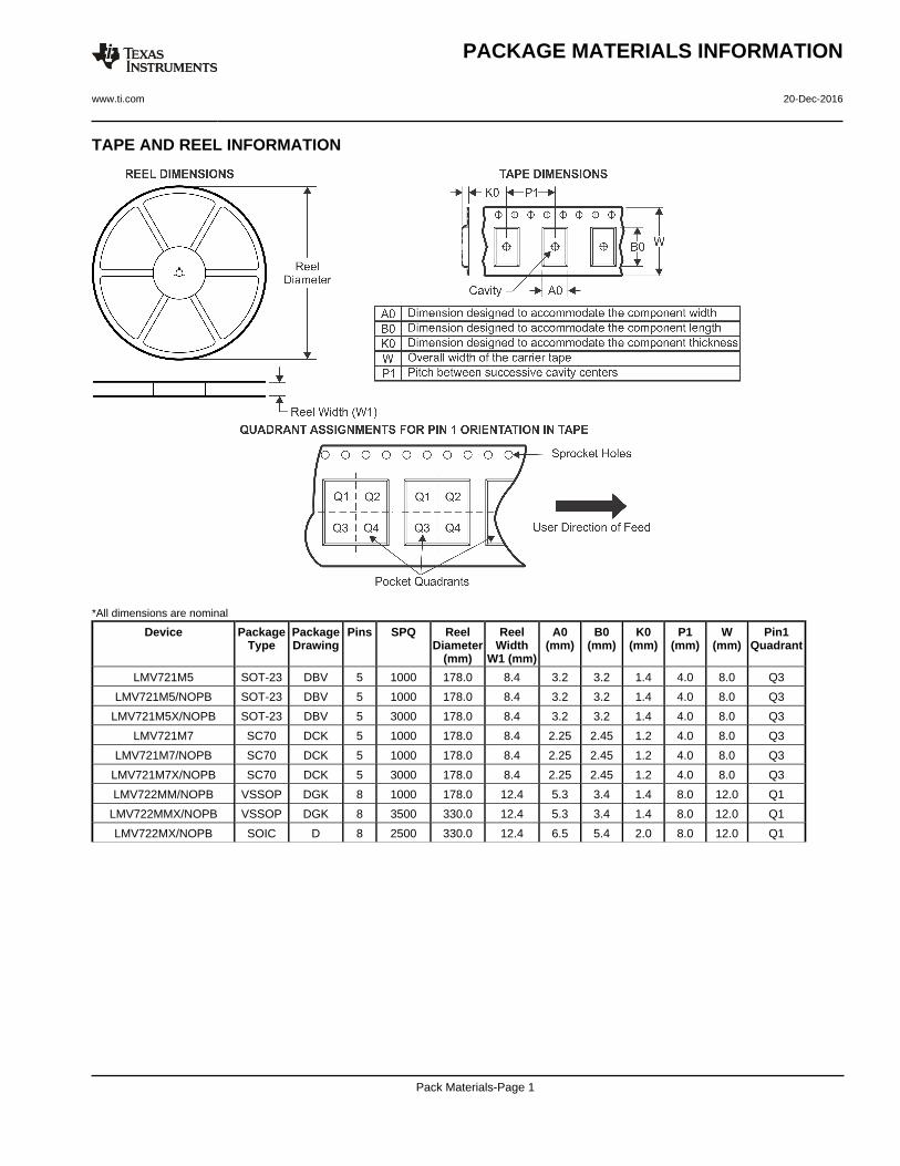
TAPE AND REEL INFORMATION
*All dimensions are nominal
Device PackageType
PackageDrawing
Pins SPQ ReelDiameter
(mm)
ReelWidth
W1 (mm)
A0(mm)
B0(mm)
K0(mm)
P1(mm)
W(mm)
Pin1Quadrant
LMV721M5 SOT-23 DBV 5 1000 178.0 8.4 3.2 3.2 1.4 4.0 8.0 Q3
LMV721M5/NOPB SOT-23 DBV 5 1000 178.0 8.4 3.2 3.2 1.4 4.0 8.0 Q3
LMV721M5X/NOPB SOT-23 DBV 5 3000 178.0 8.4 3.2 3.2 1.4 4.0 8.0 Q3
LMV721M7 SC70 DCK 5 1000 178.0 8.4 2.25 2.45 1.2 4.0 8.0 Q3
LMV721M7/NOPB SC70 DCK 5 1000 178.0 8.4 2.25 2.45 1.2 4.0 8.0 Q3
LMV721M7X/NOPB SC70 DCK 5 3000 178.0 8.4 2.25 2.45 1.2 4.0 8.0 Q3
LMV722MM/NOPB VSSOP DGK 8 1000 178.0 12.4 5.3 3.4 1.4 8.0 12.0 Q1
LMV722MMX/NOPB VSSOP DGK 8 3500 330.0 12.4 5.3 3.4 1.4 8.0 12.0 Q1
LMV722MX/NOPB SOIC D 8 2500 330.0 12.4 6.5 5.4 2.0 8.0 12.0 Q1
PACKAGE MATERIALS INFORMATION
www.ti.com 20-Dec-2016
Pack Materials-Page 1
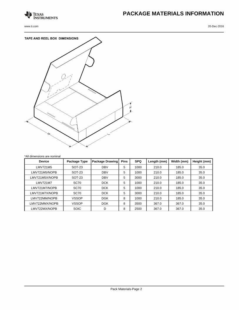
*All dimensions are nominal
Device Package Type Package Drawing Pins SPQ Length (mm) Width (mm) Height (mm)
LMV721M5 SOT-23 DBV 5 1000 210.0 185.0 35.0
LMV721M5/NOPB SOT-23 DBV 5 1000 210.0 185.0 35.0
LMV721M5X/NOPB SOT-23 DBV 5 3000 210.0 185.0 35.0
LMV721M7 SC70 DCK 5 1000 210.0 185.0 35.0
LMV721M7/NOPB SC70 DCK 5 1000 210.0 185.0 35.0
LMV721M7X/NOPB SC70 DCK 5 3000 210.0 185.0 35.0
LMV722MM/NOPB VSSOP DGK 8 1000 210.0 185.0 35.0
LMV722MMX/NOPB VSSOP DGK 8 3500 367.0 367.0 35.0
LMV722MX/NOPB SOIC D 8 2500 367.0 367.0 35.0
PACKAGE MATERIALS INFORMATION
www.ti.com 20-Dec-2016
Pack Materials-Page 2


www.ti.com
PACKAGE OUTLINE
C
TYP0.220.08
0.25
3.02.6
2X 0.95
1.9
1.45 MAX
TYP0.150.00
5X 0.50.3
TYP0.60.3
TYP80
1.9
A
3.052.75
B1.751.45
(1.1)
SOT-23 - 1.45 mm max heightDBV0005ASMALL OUTLINE TRANSISTOR
4214839/C 04/2017
NOTES: 1. All linear dimensions are in millimeters. Any dimensions in parenthesis are for reference only. Dimensioning and tolerancing per ASME Y14.5M.2. This drawing is subject to change without notice.3. Refernce JEDEC MO-178.
0.2 C A B
1
34
5
2
INDEX AREAPIN 1
GAGE PLANE
SEATING PLANE
0.1 C
SCALE 4.000
www.ti.com
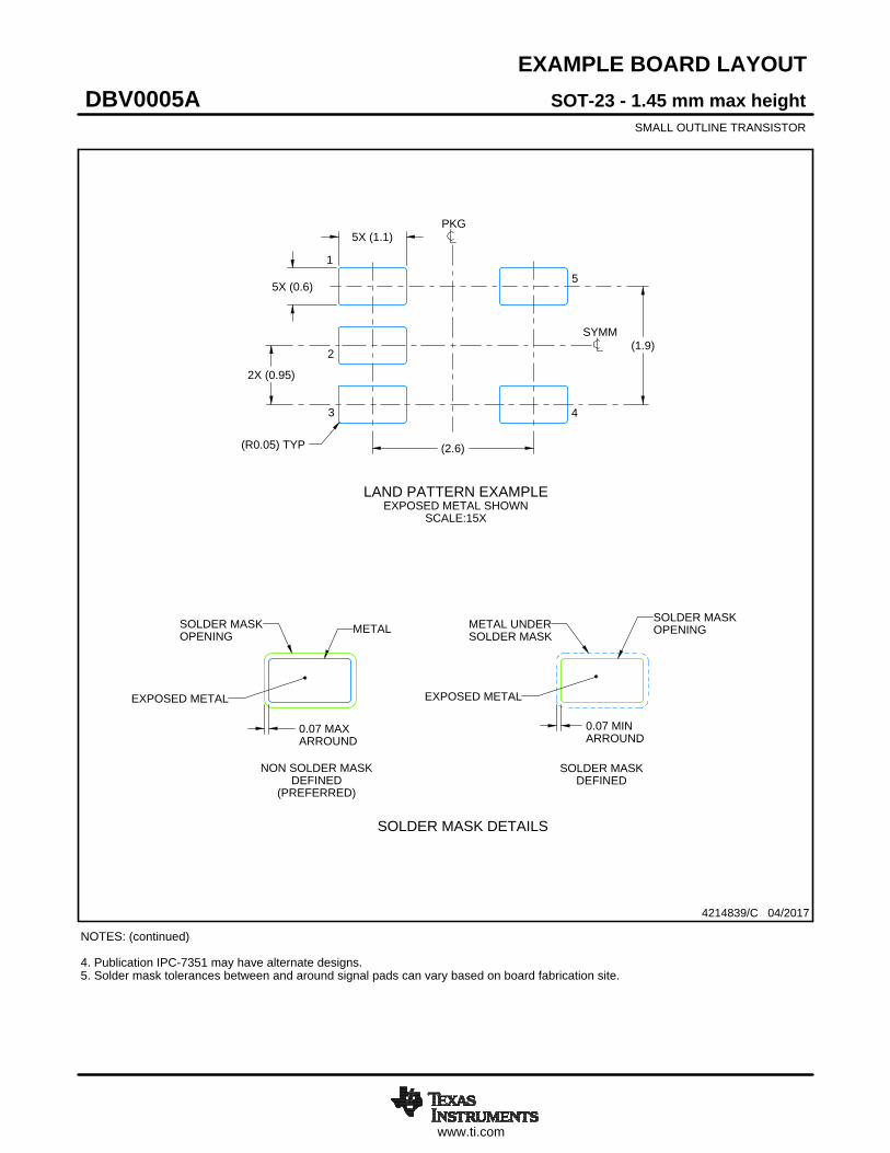
EXAMPLE BOARD LAYOUT
0.07 MAXARROUND
0.07 MINARROUND
5X (1.1)
5X (0.6)
(2.6)
(1.9)
2X (0.95)
(R0.05) TYP
4214839/C 04/2017
SOT-23 - 1.45 mm max heightDBV0005ASMALL OUTLINE TRANSISTOR
NOTES: (continued) 4. Publication IPC-7351 may have alternate designs. 5. Solder mask tolerances between and around signal pads can vary based on board fabrication site.
SYMM
LAND PATTERN EXAMPLEEXPOSED METAL SHOWN
SCALE:15X
PKG
1
3 4
5
2
SOLDER MASKOPENINGMETAL UNDER
SOLDER MASK
SOLDER MASKDEFINED
EXPOSED METAL
METALSOLDER MASKOPENING
NON SOLDER MASKDEFINED
(PREFERRED)
SOLDER MASK DETAILS
EXPOSED METAL
www.ti.com
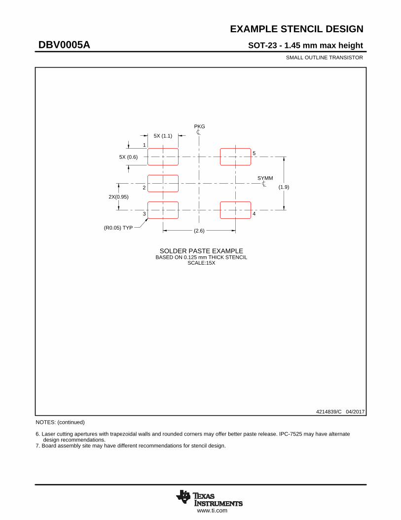
EXAMPLE STENCIL DESIGN
(2.6)
(1.9)
2X(0.95)
5X (1.1)
5X (0.6)
(R0.05) TYP
SOT-23 - 1.45 mm max heightDBV0005ASMALL OUTLINE TRANSISTOR
4214839/C 04/2017
NOTES: (continued) 6. Laser cutting apertures with trapezoidal walls and rounded corners may offer better paste release. IPC-7525 may have alternate design recommendations. 7. Board assembly site may have different recommendations for stencil design.
SOLDER PASTE EXAMPLEBASED ON 0.125 mm THICK STENCIL
SCALE:15X
SYMM
PKG
1
3 4
5
2


IMPORTANT NOTICE
Texas Instruments Incorporated (TI) reserves the right to make corrections, enhancements, improvements and other changes to itssemiconductor products and services per JESD46, latest issue, and to discontinue any product or service per JESD48, latest issue. Buyersshould obtain the latest relevant information before placing orders and should verify that such information is current and complete.TI’s published terms of sale for semiconductor products (http://www.ti.com/sc/docs/stdterms.htm) apply to the sale of packaged integratedcircuit products that TI has qualified and released to market. Additional terms may apply to the use or sale of other types of TI products andservices.Reproduction of significant portions of TI information in TI data sheets is permissible only if reproduction is without alteration and isaccompanied by all associated warranties, conditions, limitations, and notices. TI is not responsible or liable for such reproduceddocumentation. Information of third parties may be subject to additional restrictions. Resale of TI products or services with statementsdifferent from or beyond the parameters stated by TI for that product or service voids all express and any implied warranties for theassociated TI product or service and is an unfair and deceptive business practice. TI is not responsible or liable for any such statements.Buyers and others who are developing systems that incorporate TI products (collectively, “Designers”) understand and agree that Designersremain responsible for using their independent analysis, evaluation and judgment in designing their applications and that Designers havefull and exclusive responsibility to assure the safety of Designers' applications and compliance of their applications (and of all TI productsused in or for Designers’ applications) with all applicable regulations, laws and other applicable requirements. Designer represents that, withrespect to their applications, Designer has all the necessary expertise to create and implement safeguards that (1) anticipate dangerousconsequences of failures, (2) monitor failures and their consequences, and (3) lessen the likelihood of failures that might cause harm andtake appropriate actions. Designer agrees that prior to using or distributing any applications that include TI products, Designer willthoroughly test such applications and the functionality of such TI products as used in such applications.TI’s provision of technical, application or other design advice, quality characterization, reliability data or other services or information,including, but not limited to, reference designs and materials relating to evaluation modules, (collectively, “TI Resources”) are intended toassist designers who are developing applications that incorporate TI products; by downloading, accessing or using TI Resources in anyway, Designer (individually or, if Designer is acting on behalf of a company, Designer’s company) agrees to use any particular TI Resourcesolely for this purpose and subject to the terms of this Notice.TI’s provision of TI Resources does not expand or otherwise alter TI’s applicable published warranties or warranty disclaimers for TIproducts, and no additional obligations or liabilities arise from TI providing such TI Resources. TI reserves the right to make corrections,enhancements, improvements and other changes to its TI Resources. TI has not conducted any testing other than that specificallydescribed in the published documentation for a particular TI Resource.Designer is authorized to use, copy and modify any individual TI Resource only in connection with the development of applications thatinclude the TI product(s) identified in such TI Resource. NO OTHER LICENSE, EXPRESS OR IMPLIED, BY ESTOPPEL OR OTHERWISETO ANY OTHER TI INTELLECTUAL PROPERTY RIGHT, AND NO LICENSE TO ANY TECHNOLOGY OR INTELLECTUAL PROPERTYRIGHT OF TI OR ANY THIRD PARTY IS GRANTED HEREIN, including but not limited to any patent right, copyright, mask work right, orother intellectual property right relating to any combination, machine, or process in which TI products or services are used. Informationregarding or referencing third-party products or services does not constitute a license to use such products or services, or a warranty orendorsement thereof. Use of TI Resources may require a license from a third party under the patents or other intellectual property of thethird party, or a license from TI under the patents or other intellectual property of TI.TI RESOURCES ARE PROVIDED “AS IS” AND WITH ALL FAULTS. TI DISCLAIMS ALL OTHER WARRANTIES ORREPRESENTATIONS, EXPRESS OR IMPLIED, REGARDING RESOURCES OR USE THEREOF, INCLUDING BUT NOT LIMITED TOACCURACY OR COMPLETENESS, TITLE, ANY EPIDEMIC FAILURE WARRANTY AND ANY IMPLIED WARRANTIES OFMERCHANTABILITY, FITNESS FOR A PARTICULAR PURPOSE, AND NON-INFRINGEMENT OF ANY THIRD PARTY INTELLECTUALPROPERTY RIGHTS. TI SHALL NOT BE LIABLE FOR AND SHALL NOT DEFEND OR INDEMNIFY DESIGNER AGAINST ANY CLAIM,INCLUDING BUT NOT LIMITED TO ANY INFRINGEMENT CLAIM THAT RELATES TO OR IS BASED ON ANY COMBINATION OFPRODUCTS EVEN IF DESCRIBED IN TI RESOURCES OR OTHERWISE. IN NO EVENT SHALL TI BE LIABLE FOR ANY ACTUAL,DIRECT, SPECIAL, COLLATERAL, INDIRECT, PUNITIVE, INCIDENTAL, CONSEQUENTIAL OR EXEMPLARY DAMAGES INCONNECTION WITH OR ARISING OUT OF TI RESOURCES OR USE THEREOF, AND REGARDLESS OF WHETHER TI HAS BEENADVISED OF THE POSSIBILITY OF SUCH DAMAGES.Unless TI has explicitly designated an individual product as meeting the requirements of a particular industry standard (e.g., ISO/TS 16949and ISO 26262), TI is not responsible for any failure to meet such industry standard requirements.Where TI specifically promotes products as facilitating functional safety or as compliant with industry functional safety standards, suchproducts are intended to help enable customers to design and create their own applications that meet applicable functional safety standardsand requirements. Using products in an application does not by itself establish any safety features in the application. Designers mustensure compliance with safety-related requirements and standards applicable to their applications. Designer may not use any TI products inlife-critical medical equipment unless authorized officers of the parties have executed a special contract specifically governing such use.Life-critical medical equipment is medical equipment where failure of such equipment would cause serious bodily injury or death (e.g., lifesupport, pacemakers, defibrillators, heart pumps, neurostimulators, and implantables). Such equipment includes, without limitation, allmedical devices identified by the U.S. Food and Drug Administration as Class III devices and equivalent classifications outside the U.S.TI may expressly designate certain products as completing a particular qualification (e.g., Q100, Military Grade, or Enhanced Product).Designers agree that it has the necessary expertise to select the product with the appropriate qualification designation for their applicationsand that proper product selection is at Designers’ own risk. Designers are solely responsible for compliance with all legal and regulatoryrequirements in connection with such selection.Designer will fully indemnify TI and its representatives against any damages, costs, losses, and/or liabilities arising out of Designer’s non-compliance with the terms and provisions of this Notice.
Mailing Address: Texas Instruments, Post Office Box 655303, Dallas, Texas 75265Copyright © 2018, Texas Instruments Incorporated