LSN-10A D12 Models - Murata Manufacturing · Input. Input Voltage Range. 10.8-13.2 Volts (12V...
13
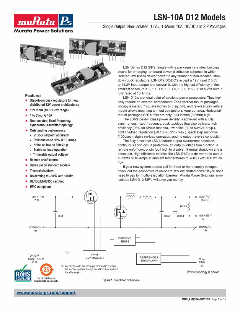
+INPUT (7,8) COMMON (6) PWM CONTROLLER CURRENT SENSE REFERENCE & ERROR AMP VCC ON/OFF CONTROL (11) VOUT TRIM (10) +OUTPUT (1,2,4) 330µF 100µF 66µF 10.5Ω +SENSE (3) COMMON (5) ➀ Features Figure 1. Simplified Schematic LSN Series D12 SIP's (single-in-line packages) are ideal building blocks for emerging, on-board power-distribution schemes in which isolated 12V buses deliver power to any number of non-isolated, step- down buck regulators. LSN D12 DC/DC's accept a 12V input (10.8V to 13.2V input range) and convert it, with the highest efficiency in the smallest space, to a 1, 1.1, 1.2, 1.3, 1.5, 1.8, 2, 2.5, 3.3 or 5 Volt output fully rated at 10 Amps. LSN D12's are ideal point-of-use/load power processors. They typi- cally require no external components. Their vertical-mount packages occupy a mere 0.7 square inches (4.5 sq. cm), and reversed pin vertical mount allows mounting to meet competitor's keep out area. Horizontal- mount packages ("H" suffix) are only 0.34 inches (8.6mm) high. The LSN's best-in-class power density is achieved with a fully synchronous, fixed-frequency, buck topology that also delivers: high efficiency (96% for 5VOUT models), low noise (30 to 50mVp-p typ.), tight line/load regulation (±0.1%/±0.25% max.), quick step response (100µsec), stable no-load operation, and no output reverse conduction. The fully functional LSN’s feature output overcurrent detection, continuous short-circuit protection, an output-voltage trim function, a remote on/off control pin (pull high to disable), thermal shutdown and a sense pin. High efficiency enables the LSN D12's to deliver rated output currents of 10 Amps at ambient temperatures to +68°C with 100 lfm air flow. If your new system boards call for three or more supply voltages, check out the economics of on-board 12V distributed power. If you don't need to pay for multiple isolation barriers, Murata Power Solutions' non- isolated LSN D12 SIP's will save you money. ■ ■ ■ ■ ■ ■ ■ ■ ■ ■ ■ Step-down buck regulators for new distributed 12V power architectures 12V input (10.8-13.2V range) 1 to 5VOUT @10A Non-isolated, fixed-frequency, synchronous-rectifier topology Outstanding performance: • ±1.25% setpoint accuracy • Efficiencies to 96% @ 10 Amps • Noise as low as 30mVp-p • Stable no-load operation • Trimmable output voltage Remote on/off control Sense pin on standard models Thermal shutdown No derating to +68°C with 100 lfm UL/IEC/EN60950 certified EMC compliant Typical topology is shown ➀ For devices with the sense-pin removed ("B" suffix), the feedback path is through the +Output pin and not the +Sense pin. www.murata-ps.com www.murata-ps.com/support For full details go to www.murata-ps.com/rohs LSN-10A D12 Models Single Output, Non-Isolated, 12VIN, 1-5VOUT, 10A, DC/DC's in SIP Packages MDC_LSN10A-D12.F03 Page 1 of 12
Transcript of LSN-10A D12 Models - Murata Manufacturing · Input. Input Voltage Range. 10.8-13.2 Volts (12V...
+INPUT(7,8)
COMMON(6)
PWMCONTROLLER
CURRENT SENSE
REFERENCE &ERROR AMP
VCC
ON/OFFCONTROL
(11)VOUT
TRIM(10)
+OUTPUT(1,2,4)
330µF100µF66µF
10.5Ω
+SENSE(3)
COMMON(5)
➀
Features
Figure 1. Simplified Schematic
LSN Series D12 SIP's (single-in-line packages) are ideal building blocks for emerging, on-board power-distribution schemes in which isolated 12V buses deliver power to any number of non-isolated, step-down buck regulators. LSN D12 DC/DC's accept a 12V input (10.8V to 13.2V input range) and convert it, with the highest efficiency in the smallest space, to a 1, 1.1, 1.2, 1.3, 1.5, 1.8, 2, 2.5, 3.3 or 5 Volt output fully rated at 10 Amps.
LSN D12's are ideal point-of-use/load power processors. They typi-cally require no external components. Their vertical-mount packages occupy a mere 0.7 square inches (4.5 sq. cm), and reversed pin vertical mount allows mounting to meet competitor's keep out area. Horizontal-mount packages ("H" suffix) are only 0.34 inches (8.6mm) high.
The LSN's best-in-class power density is achieved with a fully synchronous, fixed-frequency, buck topology that also delivers: high efficiency (96% for 5VOUT models), low noise (30 to 50mVp-p typ.), tight line/load regulation (±0.1%/±0.25% max.), quick step response (100µsec), stable no-load operation, and no output reverse conduction.
The fully functional LSN’s feature output overcurrent detection, continuous short-circuit protection, an output-voltage trim function, a remote on/off control pin (pull high to disable), thermal shutdown and a sense pin. High efficiency enables the LSN D12's to deliver rated output currents of 10 Amps at ambient temperatures to +68°C with 100 lfm air flow.
If your new system boards call for three or more supply voltages, check out the economics of on-board 12V distributed power. If you don't need to pay for multiple isolation barriers, Murata Power Solutions' non-isolated LSN D12 SIP's will save you money.
Step-down buck regulators for new distributed 12V power architectures
12V input (10.8-13.2V range)
1 to 5VOUT @10A
Non-isolated, fixed-frequency, synchronous-rectifier topology
Outstanding performance:• ±1.25% setpoint accuracy• Efficiencies to 96% @ 10 Amps• Noise as low as 30mVp-p• Stable no-load operation• Trimmable output voltage
Remote on/off control
Sense pin on standard models
Thermal shutdown
No derating to +68°C with 100 lfm
UL/IEC/EN60950 certified
EMC compliant
Typical topology is shown
➀ For devices with the sense-pin removed ("B" suffix), the feedback path is through the +Output pin and not the +Sense pin.
www.murata-ps.com
www.murata-ps.com/support
For full details go towww.murata-ps.com/rohs
LSN-10A D12 ModelsSingle Output, Non-Isolated, 12VIN, 1-5VOUT, 10A, DC/DC's in SIP Packages
MDC_LSN10A-D12.F03 Page 1 of 12
ddeluca
Discontinued
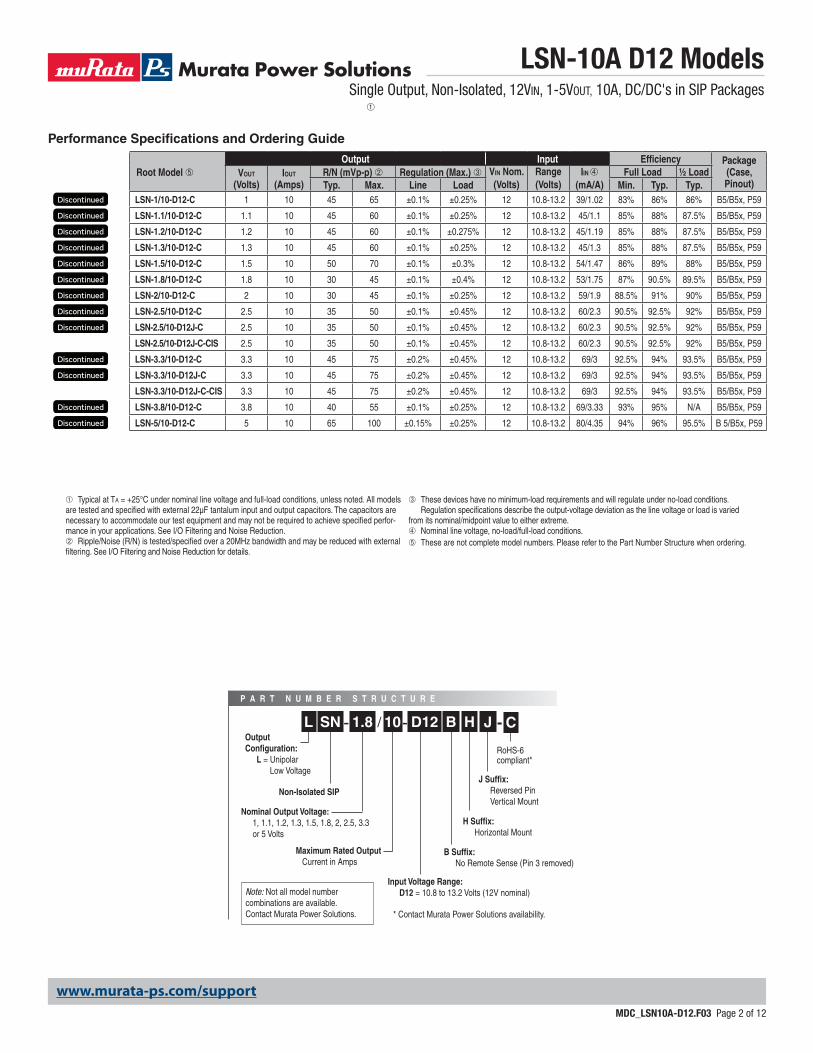
Root Model ➄Output Input Efficiency Package
(Case,Pinout)
VOUT
(Volts)IOUT
(Amps)R/N (mVp-p) ➁ Regulation (Max.) ➂ VIN Nom.
(Volts)Range(Volts)
IIN ➃
(mA/A)Full Load ½ Load
Typ. Max. Line Load Min. Typ. Typ.LSN-1/10-D12-C 1 10 45 65 ±0.1% ±0.25% 12 10.8-13.2 39/1.02 83% 86% 86% B5/B5x, P59
LSN-1.1/10-D12-C 1.1 10 45 60 ±0.1% ±0.25% 12 10.8-13.2 45/1.1 85% 88% 87.5% B5/B5x, P59
LSN-1.2/10-D12-C 1.2 10 45 60 ±0.1% ±0.275% 12 10.8-13.2 45/1.19 85% 88% 87.5% B5/B5x, P59
LSN-1.3/10-D12-C 1.3 10 45 60 ±0.1% ±0.25% 12 10.8-13.2 45/1.3 85% 88% 87.5% B5/B5x, P59
LSN-1.5/10-D12-C 1.5 10 50 70 ±0.1% ±0.3% 12 10.8-13.2 54/1.47 86% 89% 88% B5/B5x, P59
LSN-1.8/10-D12-C 1.8 10 30 45 ±0.1% ±0.4% 12 10.8-13.2 53/1.75 87% 90.5% 89.5% B5/B5x, P59
LSN-2/10-D12-C 2 10 30 45 ±0.1% ±0.25% 12 10.8-13.2 59/1.9 88.5% 91% 90% B5/B5x, P59
LSN-2.5/10-D12-C 2.5 10 35 50 ±0.1% ±0.45% 12 10.8-13.2 60/2.3 90.5% 92.5% 92% B5/B5x, P59
LSN-2.5/10-D12J-C 2.5 10 35 50 ±0.1% ±0.45% 12 10.8-13.2 60/2.3 90.5% 92.5% 92% B5/B5x, P59
LSN-2.5/10-D12J-C-CIS 2.5 10 35 50 ±0.1% ±0.45% 12 10.8-13.2 60/2.3 90.5% 92.5% 92% B5/B5x, P59
LSN-3.3/10-D12-C 3.3 10 45 75 ±0.2% ±0.45% 12 10.8-13.2 69/3 92.5% 94% 93.5% B5/B5x, P59
LSN-3.3/10-D12J-C 3.3 10 45 75 ±0.2% ±0.45% 12 10.8-13.2 69/3 92.5% 94% 93.5% B5/B5x, P59
LSN-3.3/10-D12J-C-CIS 3.3 10 45 75 ±0.2% ±0.45% 12 10.8-13.2 69/3 92.5% 94% 93.5% B5/B5x, P59
LSN-3.8/10-D12-C 3.8 10 40 55 ±0.1% ±0.25% 12 10.8-13.2 69/3.33 93% 95% N/A B5/B5x, P59
LSN-5/10-D12-C 5 10 65 100 ±0.15% ±0.25% 12 10.8-13.2 80/4.35 94% 96% 95.5% B 5/B5x, P59
➀ Typical at TA = +25°C under nominal line voltage and full-load conditions, unless noted. All models are tested and specified with external 22µF tantalum input and output capacitors. The capacitors are necessary to accommodate our test equipment and may not be required to achieve specified perfor-mance in your applications. See I/O Filtering and Noise Reduction.➁ Ripple/Noise (R/N) is tested/specified over a 20MHz bandwidth and may be reduced with external filtering. See I/O Filtering and Noise Reduction for details.
➂ These devices have no minimum-load requirements and will regulate under no-load conditions.Regulation specifications describe the output-voltage deviation as the line voltage or load is varied
from its nominal/midpoint value to either extreme.➃ Nominal line voltage, no-load/full-load conditions. ➄ These are not complete model numbers. Please refer to the Part Number Structure when ordering.
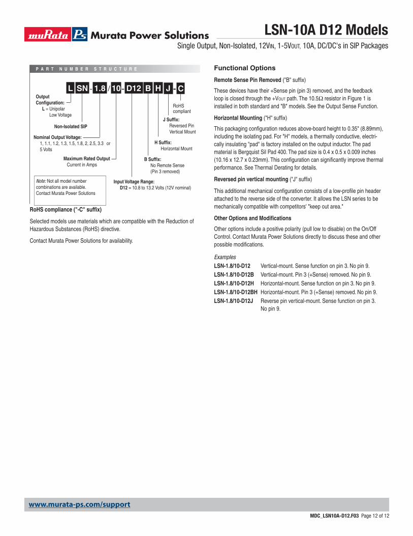
P A R T N U M B E R S T R U C T U R E
Performance Specifications and Ordering Guide
➀
Maximum Rated Output Current in Amps
Non-Isolated SIP
Output Configuration:
L = Unipolar Low Voltage
Nominal Output Voltage:1, 1.1, 1.2, 1.3, 1.5, 1.8, 2, 2.5, 3.3 or 5 Volts
Input Voltage Range: D12 = 10.8 to 13.2 Volts (12V nominal)
L SN 10- / D12 B-1.8
B Suffix:No Remote Sense (Pin 3 removed)
H
H Suffix:Horizontal Mount
J
J Suffix:Reversed PinVertical Mount
-
RoHS-6 compliant*
C
Note: Not all model number combinations are available. Contact Murata Power Solutions. * Contact Murata Power Solutions availability.
*LAST TIME BUY: 3/31/2017. CLICK HERE FOR DISCONTINUANCE NOTICES.
www.murata-ps.com/support
LSN-10A D12 ModelsSingle Output, Non-Isolated, 12VIN, 1-5VOUT, 10A, DC/DC's in SIP Packages
MDC_LSN10A-D12.F03 Page 2 of 12
ddeluca
Discontinued
ddeluca
Discontinued
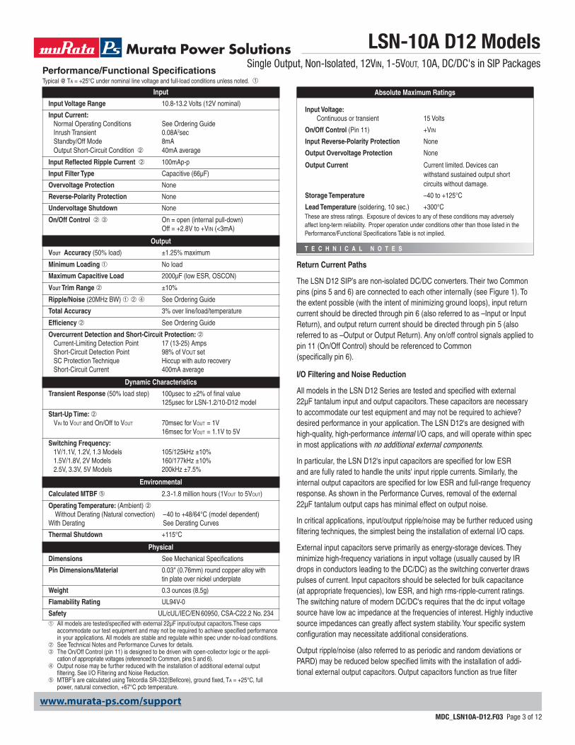
Input
Input Voltage Range 10.8-13.2 Volts (12V nominal)
Input Current: Normal Operating Conditions See Ordering Guide Inrush Transient 0.08A2sec Standby/Off Mode 8mA Output Short-Circuit Condition ➁ 40mA average
Input Reflected Ripple Current ➁ 100mAp-p
Input Filter Type Capacitive (66µF)
Overvoltage Protection None
Reverse-Polarity Protection None
Undervoltage Shutdown None
On/Off Control ➁ ➂ On = open (internal pull-down) Off = +2.8V to +VIN (<3mA)
Output
VOUT Accuracy (50% load) ±1.25% maximum
Minimum Loading ➀ No load
Maximum Capacitive Load 2000µF (low ESR, OSCON)
VOUT Trim Range ➁ ±10%
Ripple/Noise (20MHz BW) ➀ ➁ ➃ See Ordering Guide
Total Accuracy 3% over line/load/temperature
Efficiency ➁ See Ordering Guide
Overcurrent Detection and Short-Circuit Protection: ➁ Current-Limiting Detection Point 17 (13-25) Amps Short-Circuit Detection Point 98% of VOUT set SC Protection Technique Hiccup with auto recovery Short-Circuit Current 400mA average
Dynamic Characteristics
Transient Response (50% load step) 100µsec to ±2% of final value 125µsec for LSN-1.2/10-D12 model
Start-Up Time: ➁ VIN to VOUT and On/Off to VOUT 70msec for VOUT = 1V
16msec for VOUT = 1.1V to 5V
Switching Frequency: 1V/1.1V, 1.2V, 1.3 Models 105/125kHz ±10% 1.5V/1.8V, 2V Models 160/177kHz ±10% 2.5V, 3.3V, 5V Models 200kHz ±7.5%
Environmental
Calculated MTBF ➄ 2.3-1.8 million hours (1VOUT to 5VOUT)
Operating Temperature: (Ambient) ➁ Without Derating (Natural convection) –40 to +48/64°C (model dependent)With Derating See Derating Curves
Thermal Shutdown +115°C
Physical
Dimensions See Mechanical Specifications
Pin Dimensions/Material 0.03" (0.76mm) round copper alloy with tin plate over nickel underplate
Weight 0.3 ounces (8.5g)
Flamability Rating UL94V-0
Safety UL/cUL/IEC/EN 60950, CSA-C22.2 No. 234
Performance/Functional SpecificationsTypical @ TA = +25°C under nominal line voltage and full-load conditions unless noted. ➀
➀ All models are tested/specified with external 22µF input/output capacitors.These caps accommodate our test equipment and may not be required to achieve specified performance in your applications. All models are stable and regulate within spec under no-load conditions.
➁ See Technical Notes and Performance Curves for details.➂ The On/Off Control (pin 11) is designed to be driven with open-collector logic or the appli- cation of appropriate voltages (referenced to Common, pins 5 and 6). ➃ Output noise may be further reduced with the installation of additional external output
filtering. See I/O Filtering and Noise Reduction.➄ MTBF’s are calculated using Telcordia SR-332(Bellcore), ground fixed, TA = +25°C, full
power, natural convection, +67°C pcb temperature.
T E C H N I C A L N O T E S
Input Voltage:Continuous or transient 15 Volts
On/Off Control (Pin 11) +VIN
Input Reverse-Polarity Protection None
Output Overvoltage Protection None
Output Current Current limited. Devices can withstand sustained output short circuits without damage.
Storage Temperature –40 to +125°C
Lead Temperature (soldering, 10 sec.) +300°CThese are stress ratings. Exposure of devices to any of these conditions may adversely affect long-term reliability. Proper operation under conditions other than those listed in the Performance/Functional Specifications Table is not implied.
Absolute Maximum Ratings
Return Current Paths
The LSN D12 SIP’s are non-isolated DC/DC converters. Their two Common pins (pins 5 and 6) are connected to each other internally (see Figure 1). To the extent possible (with the intent of minimizing ground loops), input return current should be directed through pin 6 (also referred to as –Input or Input Return), and output return current should be directed through pin 5 (also referred to as –Output or Output Return). Any on/off control signals applied to pin 11 (On/Off Control) should be referenced to Common (specifically pin 6).
I/O Filtering and Noise Reduction
All models in the LSN D12 Series are tested and specified with external 22µF tantalum input and output capacitors. These capacitors are necessary to accommodate our test equipment and may not be required to achieve? desired performance in your application. The LSN D12's are designed with high-quality, high-performance internal I/O caps, and will operate within spec in most applications with no additional external components.
In particular, the LSN D12's input capacitors are specified for low ESR and are fully rated to handle the units' input ripple currents. Similarly, the internal output capacitors are specified for low ESR and full-range frequency response. As shown in the Performance Curves, removal of the external 22µF tantalum output caps has minimal effect on output noise.
In critical applications, input/output ripple/noise may be further reduced using filtering techniques, the simplest being the installation of external I/O caps.
External input capacitors serve primarily as energy-storage devices. They minimize high-frequency variations in input voltage (usually caused by IR drops in conductors leading to the DC/DC) as the switching converter draws pulses of current. Input capacitors should be selected for bulk capacitance (at appropriate frequencies), low ESR, and high rms-ripple-current ratings. The switching nature of modern DC/DC's requires that the dc input voltage source have low ac impedance at the frequencies of interest. Highly inductive source impedances can greatly affect system stability. Your specific system configuration may necessitate additional considerations.
Output ripple/noise (also referred to as periodic and random deviations or PARD) may be reduced below specified limits with the installation of addi-tional external output capacitors. Output capacitors function as true filter
www.murata-ps.com/support
LSN-10A D12 ModelsSingle Output, Non-Isolated, 12VIN, 1-5VOUT, 10A, DC/DC's in SIP Packages
MDC_LSN10A-D12.F03 Page 3 of 12
elements and should be selected for bulk capacitance, low ESR, and appro-priate frequency response. Any scope measurements of PARD should be made directly at the DC/DC output pins with scope probe ground less than 0.5" in length.
All external capacitors should have appropriate voltage ratings and be located as close to the converters as possible. Temperature variations for all relevant parameters should be taken into consideration.
The most effective combination of external I/O capacitors will be a function of your line voltage and source impedance, as well as your particular load and layout conditions. Our Applications Engineers can recommend potential solu-tions and discuss the possibility of our modifying a given device’s internal filter-ing to meet your specific requirements. Contact our Applications Engineering Group for additional details.
Input Fusing
Most applications and or safety agencies require the installation of fuses at the inputs of power conversion components. LSN D12 Series DC/DC converters are not internally fused. Therefore, if input fusing is mandatory, either a normal-blow or a slow-blow fuse with a value no greater than 9 Amps should be installed within the ungrounded input path to the converter.
As a rule of thumb however, we recommend to use a normal-blow or slow-blow fuse with a typical value of about twice the maximum input current, calculated at low line with the converters minimum efficiency.
Safety Considerations
LSN D12 SIP's are non-isolated DC/DC converters. In general, all DC/DC's must be installed, including considerations for I/O voltages and spacing/separation requirements, in compliance with relevant safety-agency speci- fications (usually UL/IEC/EN60950).
In particular, for a non-isolated converter's output voltage to meet SELV (safety extra low voltage) requirements, its input must be SELV compliant. If the output needs to be ELV (extra low voltage), the input must be ELV.
Input Overvoltage and Reverse-Polarity Protection
LSN D12 SIP Series DC/DC's do not incorporate either input overvoltage or input reverse-polarity protection. Input voltages in excess of the specified absolute maximum ratings and input polarity reversals of longer than "instan-taneous" duration can cause permanent damage to these devices.
Start-Up Time
The VIN to VOUT Start-Up Time is the interval between the time at which a ramping input voltage crosses the lower limit of the specified input voltage range (10.8 Volts) and the fully loaded output voltage enters and remains within its specified accuracy band. Actual measured times will vary with input source impedance, external input capacitance, and the slew rate and final value of the input voltage as it appears to the converter.
The On/Off to VOUT Start-Up Time assumes the converter is turned off via the On/Off Control with the nominal input voltage already applied to the converter. The specification defines the interval between the time at which the converter is turned on and the fully loaded output voltage enters and remains within its specified accuracy band. See Typical Performance Curves.
On/Off Control and Power-up Sequencing
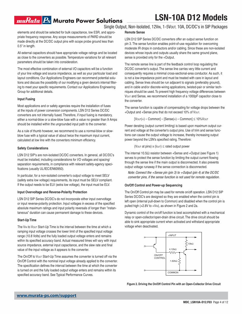
The On/Off Control pin may be used for remote on/off operation. LSN D12 SIP Series DC/DC's are designed so they are enabled when the control pin is left open (internal pull-down to Common) and disabled when the control pin is pulled high (+2.8V to +VIN), as shown in Figure 2 and 2a.
Dynamic control of the on/off function is best accomplished with a mechanical relay or open-collector/open-drain drive circuit. The drive circuit should be able to sink appropriate current when activated and withstand appropriate voltage when deactivated.
Figure 2. Driving the On/Off Control Pin with an Open-Collector Drive Circuit
+INPUT
COMMON
10kΩ
4.12kΩ
1.62kΩ
ON/OFFCONTROL
Remote Sense
LSN D12 SIP Series DC/DC converters offer an output sense function on pin 3. The sense function enables point-of-use regulation for overcoming moderate IR drops in conductors and/or cabling. Since these are non-isolated devices whose inputs and outputs usually share the same ground plane, sense is provided only for the +Output.
The remote sense line is part of the feedback control loop regulating the DC/DC converter’s output. The sense line carries very little current and consequently requires a minimal cross-sectional-area conductor. As such, it is not a low-impedance point and must be treated with care in layout and cabling. Sense lines should be run adjacent to signals (preferably ground), and in cable and/or discrete-wiring applications, twisted-pair or similar tech-niques should be used. To prevent high frequency voltage differences between VOUT and Sense, we recommend installation of a 1000pF capacitor close to the converter.
The sense function is capable of compensating for voltage drops between the +Output and +Sense pins that do not exceed 10% of VOUT.
[VOUT(+) – Common] – [Sense(+) – Common] ≤ 10%VOUT
Power derating (output current limiting) is based upon maximum output cur-rent and voltage at the converter's output pins. Use of trim and sense func-tions can cause the output voltage to increase, thereby increasing output power beyond the LSN's specified rating. Therefore:
(VOUT at pins) x (IOUT) ≤ rated output power
The internal 10.5Ω resistor between +Sense and +Output (see Figure 1) serves to protect the sense function by limiting the output current flowing through the sense line if the main output is disconnected. It also prevents output voltage runaway if the sense connection is disconnected.
Note: Connect the +Sense pin (pin 3) to +Output (pin 4) at the DC/DC converter pins, if the sense function is not used for remote regulation.
www.murata-ps.com/support
LSN-10A D12 ModelsSingle Output, Non-Isolated, 12VIN, 1-5VOUT, 10A, DC/DC's in SIP Packages
MDC_LSN10A-D12.F03 Page 4 of 12
Output Voltage Trimming
Allowable trim ranges for each model in the LSN D12 SIP Series are ±10%. Trimming is accomplished with either a trimpot or a single fixed resistor. The trimpot should be connected between +Output and Common with its wiper connected to the Trim pin as shown in Figure 3 below.
A trimpot can be used to determine the value of a single fixed resistor which can then be connected, as shown in Figure 4, between the Trim pin and +Output to trim down the output voltage, or between the Trim pin and Common to trim up the output voltage. Fixed resistors should have absolute TCR’s less than 100ppm/°C to ensure stability.
Figure 4. Trim Connections Using Fixed Resistors
Note: Install either a fixed trim-up resistor or a fixed trim-down resistor depending upon desired output voltage.
Output Overvoltage Protection
LSN D12 SIP Series DC/DC converters do not incorporate output overvolt-age protection. In the extremely rare situation in which the device’s feedback loop is broken, the output voltage may run to excessively high levels (VOUT = VIN). If it is absolutely imperative that you protect your load against any and all possible overvoltage situations, voltage limiting circuitry must be provided external to the power converter.
Output Overcurrent Detection
Overloading the output of a power converter for an extended period of time will invariably cause internal component temperatures to exceed their maximum ratings and eventually lead to component failure. High-current-carrying components such as inductors, FET's and diodes are at the highest risk. LSN D12 SIP Series DC/DC converters incorporate an output overcur-rent detection and shutdown function that serves to protect both the power converter and its load.
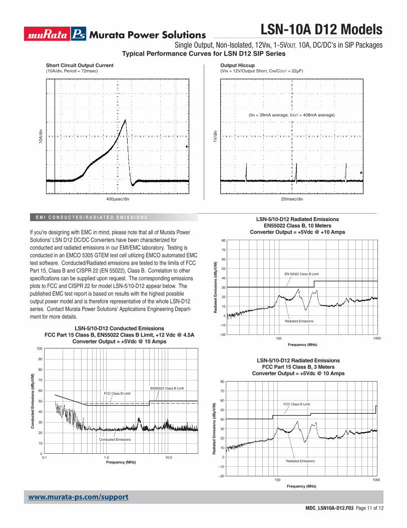
If the output current exceeds it maximum rating by typically 70% (17 Amps) or if the output voltage drops to less than 98% of it original value, the LSN D12's internal overcurrent-detection circuitry immediately turns off the converter, which then goes into a "hiccup" mode. While hiccupping, the converter will continuously attempt to restart itself, go into overcurrent, and then shut down. Under these conditions, the average output current will be approximately 400mA, and the average input current will be approximately 40mA. Once the output short is removed, the converter will automatically restart itself.
Figure 3. Trim Connections Using a Trimpot
LOAD20kΩ5-10Turns
+INPUT
COMMON
COMMON
+OUTPUT
TRIM
TrimDown
Trim Up
LOAD
+INPUT
COMMON
+OUTPUT
TRIM
COMMON
Trim Equations
Note: Resistor values are in kΩ. Accuracy of adjustment is subject to tolerances of resistors and factory-adjusted, initial output accuracy.
VO = desired output voltage. VONOM = nominal output voltage.
The equations below can be used as starting points for selecting specific trim-resistor values. Recall, untrimmed devices are guaranteed to be ±1% accurate.
Adjustment beyond the specified ±10% adjustment range is not recommended.
UPVO – VO NOM
RT (kΩ) =1.46
DOWN VO NOM – VORT (kΩ) = – X
– X
1.82(VO – 0.8)
UPVO – VO NOM
RT (kΩ) =3.72
DOWN VO NOM – VORT (kΩ) = – X
– X
4.64(VO – 0.8)
UPVO – VO NOM
RT (kΩ) =6
DOWN VO NOM – VORT (kΩ) = – X
– X
7.5(VO – 0.8)
LSN-1/10-D12: X = 0.909LSN-1.1/10-D12: X = 2.49LSN-1.2/10-D12: X = 3.09LSN-1.3/10-D12: X = 4.12
LSN-1.5/10-D12: X = 13.3LSN-1.8/10-D12: X = 16.9LSN-2/10-D12: X = 15.4
LSN-2.5/10-D12: X = 20LSN-3.3/10-D12: X = 15LSN-5/10-D12: X = 10
The on/off control function, however, can be externally inverted so that the converter will be disabled while the input voltage is ramping up and then "released" once the input has stabilized.
For a controlled start-up of one or more LSN-D12's, or if several output voltages need to be powered-up in a given sequence, the On/Off Control pin can be pulled high (external pull-up resistor, converter disabled) and then driven low with an external open collector device to enable the converter.
Figure 2a. Inverting On/Off Control Pin Signal and Power-Up Sequencing
+INPUT
COMMON
10kΩ
4.12kΩ
5.6kΩ
1.62kΩ
ON/OFFCONTROL
www.murata-ps.com/support
LSN-10A D12 ModelsSingle Output, Non-Isolated, 12VIN, 1-5VOUT, 10A, DC/DC's in SIP Packages
MDC_LSN10A-D12.F03 Page 5 of 12
Thermal Considerations and Thermal Protection
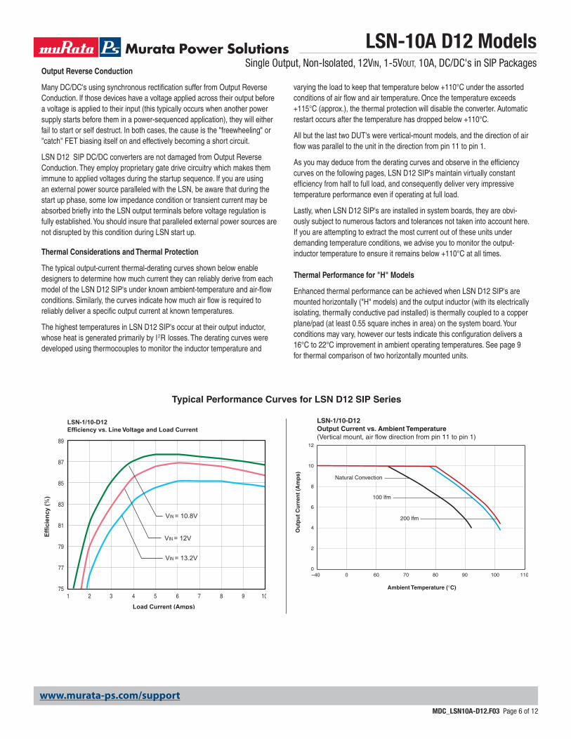
The typical output-current thermal-derating curves shown below enable designers to determine how much current they can reliably derive from each model of the LSN D12 SIP's under known ambient-temperature and air-flow conditions. Similarly, the curves indicate how much air flow is required to reliably deliver a specific output current at known temperatures.
The highest temperatures in LSN D12 SIP's occur at their output inductor, whose heat is generated primarily by I2R losses. The derating curves were developed using thermocouples to monitor the inductor temperature and
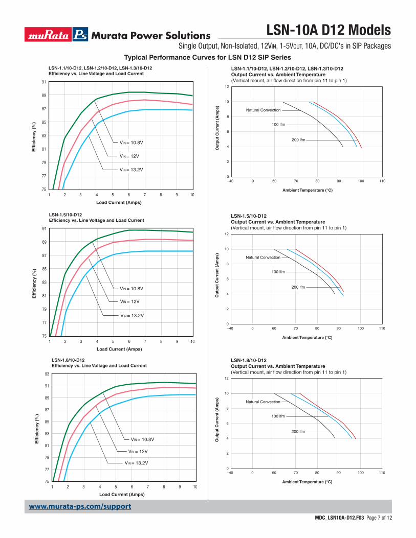
Typical Performance Curves for LSN D12 SIP Series
89
87
85
83
81
79
77
75
LSN-1/10-D12Efficiency vs. Line Voltage and Load Current
1 2 3 4 5 6 7 8 9 10
Load Current (Amps)
Eff
icie
ncy
(%
)
VIN = 10.8V
VIN = 12V
VIN = 13.2V
–40 0 60 70 80 90 100 110
LSN-1/10-D12Output Current vs. Ambient Temperature(Vertical mount, air flow direction from pin 11 to pin 1)
Ou
tpu
t C
urr
ent
(Am
ps)
Ambient Temperature (°C)
12
10
8
6
4
2
0
Natural Convection
200 lfm
100 lfm
Output Reverse Conduction
Many DC/DC's using synchronous rectification suffer from Output Reverse Conduction. If those devices have a voltage applied across their output before a voltage is applied to their input (this typically occurs when another power supply starts before them in a power-sequenced application), they will either fail to start or self destruct. In both cases, the cause is the "freewheeling" or "catch" FET biasing itself on and effectively becoming a short circuit.
LSN D12 SIP DC/DC converters are not damaged from Output Reverse Conduction. They employ proprietary gate drive circuitry which makes them immune to applied voltages during the startup sequence. If you are using an external power source paralleled with the LSN, be aware that during the start up phase, some low impedance condition or transient current may be absorbed briefly into the LSN output terminals before voltage regulation is fully established. You should insure that paralleled external power sources are not disrupted by this condition during LSN start up.
varying the load to keep that temperature below +110°C under the assorted conditions of air flow and air temperature. Once the temperature exceeds +115°C (approx.), the thermal protection will disable the converter. Automaticrestart occurs after the temperature has dropped below +110°C.
All but the last two DUT's were vertical-mount models, and the direction of air flow was parallel to the unit in the direction from pin 11 to pin 1.
As you may deduce from the derating curves and observe in the efficiency curves on the following pages, LSN D12 SIP's maintain virtually constant efficiency from half to full load, and consequently deliver very impressive temperature performance even if operating at full load.
Lastly, when LSN D12 SIP's are installed in system boards, they are obvi-ously subject to numerous factors and tolerances not taken into account here. If you are attempting to extract the most current out of these units under demanding temperature conditions, we advise you to monitor the output-inductor temperature to ensure it remains below +110°C at all times.
Thermal Performance for "H" Models
Enhanced thermal performance can be achieved when LSN D12 SIP's are mounted horizontally ("H" models) and the output inductor (with its electrically isolating, thermally conductive pad installed) is thermally coupled to a copper plane/pad (at least 0.55 square inches in area) on the system board. Your conditions may vary, however our tests indicate this configuration delivers a 16°C to 22°C improvement in ambient operating temperatures. See page 9 for thermal comparison of two horizontally mounted units.
www.murata-ps.com/support
LSN-10A D12 ModelsSingle Output, Non-Isolated, 12VIN, 1-5VOUT, 10A, DC/DC's in SIP Packages
MDC_LSN10A-D12.F03 Page 6 of 12
91
89
87
85
83
81
79
77
75
LSN-1.1/10-D12, LSN-1.2/10-D12, LSN-1.3/10-D12Efficiency vs. Line Voltage and Load Current
1 2 3 4 5 6 7 8 9 10
Load Current (Amps)
Eff
icie
ncy
(%
)
VIN = 10.8V
VIN = 12V
VIN = 13.2V
–40 0 60 70 80 90 100 110
LSN-1.1/10-D12, LSN-1.2/10-D12, LSN-1.3/10-D12Output Current vs. Ambient Temperature(Vertical mount, air flow direction from pin 11 to pin 1)
Ou
tpu
t C
urr
ent
(Am
ps)
Ambient Temperature (°C)
12
10
8
6
4
2
0
Natural Convection
200 lfm
100 lfm
91
89
87
85
83
81
79
77
75
LSN-1.5/10-D12Efficiency vs. Line Voltage and Load Current
1 2 3 4 5 6 7 8 9 10
Load Current (Amps)
Eff
icie
ncy
(%
)
VIN = 10.8V
VIN = 12V
VIN = 13.2V
93
91
89
87
85
83
81
79
77
75
LSN-1.8/10-D12Efficiency vs. Line Voltage and Load Current
1 2 3 4 5 6 7 8 9 10
Load Current (Amps)
Eff
icie
ncy
(%
)
VIN = 10.8V
VIN = 12V
VIN = 13.2V
Typical Performance Curves for LSN D12 SIP Series
–40 0 60 70 80 90 100 110
LSN-1.5/10-D12Output Current vs. Ambient Temperature(Vertical mount, air flow direction from pin 11 to pin 1)
Ou
tpu
t C
urr
ent
(Am
ps)
Ambient Temperature (°C)
12
10
8
6
4
2
0
Natural Convection
200 lfm
100 lfm
–40 0 60 70 80 90 100 110
LSN-1.8/10-D12Output Current vs. Ambient Temperature(Vertical mount, air flow direction from pin 11 to pin 1)
Ou
tpu
t C
urr
ent
(Am
ps)
Ambient Temperature (°C)
12
10
8
6
4
2
0
Natural Convection
200 lfm
100 lfm
www.murata-ps.com/support
LSN-10A D12 ModelsSingle Output, Non-Isolated, 12VIN, 1-5VOUT, 10A, DC/DC's in SIP Packages
MDC_LSN10A-D12.F03 Page 7 of 12
95
93
91
89
87
85
83
81
79
77
75
LSN-3.3/10-D12Efficiency vs. Line Voltage and Load Current
1 2 3 4 5 6 7 8 9 10
Load Current (Amps)
Eff
icie
ncy
(%
)
VIN = 10.8V
VIN = 12V
VIN = 13.2V
94
92
90
88
86
84
82
80
78
76
74
LSN-2.5/10-D12Efficiency vs. Line Voltage and Load Current
1 2 3 4 5 6 7 8 9 10
Load Current (Amps)
Eff
icie
ncy
(%
)
VIN = 10.8V
VIN = 12V
VIN = 13.2V
Typical Performance Curves for LSN D12 SIP Series
–40 0 50 60 70 80 90 100 110
LSN-2.5/10-D12Output Current vs. Ambient Temperature(Vertical mount, air flow direction from pin 11 to pin 1)
Ou
tpu
t C
urr
ent
(Am
ps)
Ambient Temperature (°C)
12
10
8
6
4
2
0
Natural Convection
200 lfm
100 lfm
–40 0 50 60 70 80 90 100 110
LSN-3.3/10-D12Output Current vs. Ambient Temperature(Vertical mount, air flow direction from pin 11 to pin 1)
Ou
tpu
t C
urr
ent
(Am
ps)
Ambient Temperature (°C)
12
10
8
6
4
2
0
Natural Convection
200 lfm
100 lfm
93
91
89
87
85
83
81
79
77
75
LSN-2/10-D12Efficiency vs. Line Voltage and Load Current
1 2 3 4 5 6 7 8 9 10
Load Current (Amps)
Eff
icie
ncy
(%
)
VIN = 10.8V
VIN = 12V
VIN = 13.2V
–40 0 50 60 70 80 90 100 110
LSN-2/10-D12Output Current vs. Ambient Temperature(Vertical mount, air flow direction from pin 11 to pin 1)
Ou
tpu
t C
urr
ent
(Am
ps)
Ambient Temperature (°C)
12
10
8
6
4
2
0
Natural Convection
200 lfm
100 lfm
www.murata-ps.com/support
LSN-10A D12 ModelsSingle Output, Non-Isolated, 12VIN, 1-5VOUT, 10A, DC/DC's in SIP Packages
MDC_LSN10A-D12.F03 Page 8 of 12
98
96
94
92
90
88
86
84
82
LSN-5/10-D12Efficiency vs. Line Voltage and Load Current
1 2 3 4 5 6 7 8 9 10
Load Current (Amps)
Eff
icie
ncy
(%
)
VIN = 10.8V
VIN = 12V
VIN = 13.2V
–40 0 40 50 60 70 80 90 100
LSN-5/10-D12Output Current vs. Ambient Temperature(Vertical mount, air flow direction from pin 11 to pin 1)
Ou
tpu
t C
urr
ent
(Am
ps)
Ambient Temperature (°C)
12
10
8
6
4
2
0
Natural Convection
200 lfm
100 lfm
–40 0 50 60 70 80 90 100 110
LSN-1/10-D12H (Horizontal Mount)Output Current vs. Ambient Temperature(Air flow direction from pin 11 to pin 1)
Ou
tpu
t C
urr
ent
(Am
ps)
Ambient Temperature (°C)
12
10
8
6
4
2
0
Natural Convection
200 lfm
100 lfm
–40 0 40 50 60 70 80 90 100
LSN-5/10-D12H (Horizontal Mount)Output Current vs. Ambient Temperature(Air flow direction from pin 11 to pin 1)
Ou
tpu
t C
urr
ent
(Am
ps)
Ambient Temperature (°C)
12
10
8
6
4
2
0
Natural Convection
200 lfm
100 lfm
Input Reflected Ripple Current(VIN = 12V, VOUT = 5V/10A, CIN/COUT = 22µF)
2µsec/div
20m
A/d
iv
Input Inrush Current(VIN = 12V, 7000µF as Input Switch)
10µsec/div
20A
/div
Typical Performance Curves for LSN D12 SIP Series
www.murata-ps.com/support
LSN-10A D12 ModelsSingle Output, Non-Isolated, 12VIN, 1-5VOUT, 10A, DC/DC's in SIP Packages
MDC_LSN10A-D12.F03 Page 9 of 12
Dynamic Load Response(VIN = 12V, VOUT = 5V/50 to 100% Load Step, CIN/COUT = 22µF)
100µs/div
20m
V/d
iv
Channel 2
Channel 1
Dynamic Load Response(VIN = 12V, VOUT = 5V, 0 - 100% Load Step, CIN = 22µF, COUT = 2000µF OSCON)
100µs/div
50m
V/d
iv
Channel 2
Channel 1
Output Ripple Noise(VIN = 12V, VOUT = 5V, Full Load, COUT = 22µF)
1µsec/div
10m
V/d
iv
Output Ripple/Noise(VIN = 12V, VOUT = 5V, Full Load, COUT = 2000µF OSCON)
1µsec/div
10m
V/d
iv
Typical Performance Curves for LSN D12 SIP Series
Power-Up From VIN(VIN = 12V, VOUT = 5V/10A, CIN = 22µF, Output Filter 22µF-700nH-150µF)
4msec/div
Cha
nnel
1:
2V/d
ivC
hann
el 2
: 5V
/div
Power-Up From VIN(VIN = 12V, VOUT = 5V/10A, CIN = 22µF, COUT = 2000µF OSCON)
4msec/div
Cha
nnel
1:
2V/d
ivC
hann
el 2
: 5V
/div
www.murata-ps.com/support
LSN-10A D12 ModelsSingle Output, Non-Isolated, 12VIN, 1-5VOUT, 10A, DC/DC's in SIP Packages
MDC_LSN10A-D12.F03 Page 10 of 12
Output Hiccup(VIN = 12V/Output Short, CIN/COUT = 22µF)
20msec/div
1V/d
iv
(IIN = 39mA average, IOUT = 408mA average)
Short Circuit Output Current(10A/div, Period = 72msec)
400µsec/div
10A
/div
LSN-5/10-D12 Radiated EmissionsEN55022 Class B, 10 Meters
Converter Output = +5Vdc @ +10 Amps80
70
60
50
40
30
20
10
0
–10
–20
Frequency (MHz)
100 1000
Radiated Emissions
EN 55022 Class B Limit
Rad
iate
d E
mis
sion
s (d
BµV
/M)
80
70
60
50
40
30
20
10
0
–10
–20
Frequency (MHz)
100 1000
FCC Class B Limit
LSN-5/10-D12 Radiated EmissionsFCC Part 15 Class B, 3 Meters
Converter Output = +5Vdc @ 10 Amps
Rad
iate
d E
mis
sion
s (d
BµV
/M)
Radiated Emissions
If you’re designing with EMC in mind, please note that all of Murata Power Solutions' LSN D12 DC/DC Converters have been characterized for conducted and radiated emissions in our EMI/EMC laboratory. Testing is conducted in an EMCO 5305 GTEM test cell utilizing EMCO automated EMC test software. Conducted/Radiated emissions are tested to the limits of FCC Part 15, Class B and CISPR 22 (EN 55022), Class B. Correlation to other specifications can be supplied upon request. The corresponding emissions plots to FCC and CISPR 22 for model LSN-5/10-D12 appear below. The published EMC test report is based on results with the highest possible output power model and is therefore representative of the whole LSN-D12 series. Contact Murata Power Solutions' Applications Engineering Depart-ment for more details.
E M I C O N D U C T E D / R A D I A T E D E M I S S I O N S
100
90
80
70
60
50
40
30
20
10
0
Frequency (MHz)0.1 1.0 10.0
LSN-5/10-D12 Conducted EmissionsFCC Part 15 Class B, EN55022 Class B Limit, +12 Vdc @ 4.5A
Converter Output = +5Vdc @ 10 Amps
Con
duct
ed E
mis
sion
s (d
BµV
/M)
Conducted Emissions
FCC Class B Limit
EN55022 Class B Limit
Typical Performance Curves for LSN D12 SIP Series
www.murata-ps.com/support
LSN-10A D12 ModelsSingle Output, Non-Isolated, 12VIN, 1-5VOUT, 10A, DC/DC's in SIP Packages
MDC_LSN10A-D12.F03 Page 11 of 12
Functional Options
Remote Sense Pin Removed ("B" suffix)
These devices have their +Sense pin (pin 3) removed, and the feedback loop is closed through the +VOUT path. The 10.5Ω resistor in Figure 1 is installed in both standard and "B" models. See the Output Sense Function.
Horizontal Mounting ("H" suffix)
This packaging configuration reduces above-board height to 0.35" (8.89mm), including the isolating pad. For "H" models, a thermally conductive, electri-cally insulating "pad" is factory installed on the output inductor. The pad material is Bergquist Sil Pad 400. The pad size is 0.4 x 0.5 x 0.009 inches (10.16 x 12.7 x 0.23mm). This configuration can significantly improve thermal performance. See Thermal Derating for details.
Reversed pin vertical mounting ("J" suffix)
This additional mechanical configuration consists of a low-profile pin header attached to the reverse side of the converter. It allows the LSN series to be mechanically compatible with competitors' "keep out area."
Other Options and Modifications
Other options include a positive polarity (pull low to disable) on the On/Off Control. Contact Murata Power Solutions directly to discuss these and other possible modifications.
ExamplesLSN-1.8/10-D12 Vertical-mount. Sense function on pin 3. No pin 9.LSN-1.8/10-D12B Vertical-mount. Pin 3 (+Sense) removed. No pin 9.LSN-1.8/10-D12H Horizontal-mount. Sense function on pin 3. No pin 9.LSN-1.8/10-D12BH Horizontal-mount. Pin 3 (+Sense) removed. No pin 9.LSN-1.8/10-D12J Reverse pin vertical-mount. Sense function on pin 3.
No pin 9.
RoHS compliance ("-C" suffix)
Selected models use materials which are compatible with the Reduction of Hazardous Substances (RoHS) directive.
Contact Murata Power Solutions for availability.
P A R T N U M B E R S T R U C T U R E
Maximum Rated Output Current in Amps
Non-Isolated SIP
Output Configuration:
L = Unipolar Low Voltage
Nominal Output Voltage:1, 1.1, 1.2, 1.3, 1.5, 1.8, 2, 2.5, 3.3 or 5 Volts
Input Voltage Range: D12 = 10.8 to 13.2 Volts (12V nominal)
L SN 10- / D12 B-1.8
B Suffix:No Remote Sense (Pin 3 removed)
H
H Suffix:Horizontal Mount
J
J Suffix:Reversed PinVertical Mount
-
RoHS compliant
C
Note: Not all model number combinations are available. Contact Murata Power Solutions
www.murata-ps.com/support
LSN-10A D12 ModelsSingle Output, Non-Isolated, 12VIN, 1-5VOUT, 10A, DC/DC's in SIP Packages
MDC_LSN10A-D12.F03 Page 12 of 12
1 2 3 4 5 76 8 9 10 11
2.00(50.80)
0.030 ±0.001 DIA.(0.762 ±0.025)
0.55(13.97)
0.34(8.64)
0.20(5.08)
0.110(2.79)
0.046(1.17)
0.05(1.27)
0.400(10.16)
4 EQ. SP. @0.100 (2.54)
0.500(12.70)
5 EQ. SP. @0.100 (2.54)
1.000(25.40)
0.17(4.32)
LAYOUT PATTERNTOP VIEW
0.34(8.64)
0.25(6.35)
M E C H A N I C A L S P E C I F I C A T I O N S
Case B5 Vertical Mounting
(Standard)
* Pin 3 (+Sense) removedfor "B" suffix models.
0.35(8.89)
0.21(5.33)
0.16(4.06)
0.360(9.14)
1 2 3 4 5 76 8 9
ISOLATINGPAD
10 11
2.00(50.80)
0.030 ±0.001 DIA.(0.762 ±0.025)
0.55(13.97)
0.05(1.27)
0.05(1.27)
0.55(13.97)
0.50(12.7)
0.400(10.16)
0.56(14.22)
0.53(13.46)
4 EQ. SP. @0.100 (2.54)
0.500(12.70)
5 EQ. SP. @0.100 (2.54)
1.000(25.40)
LAYOUT PATTERN TOP VIEWRECOMMENDED
COPPER PADON PCB (0.55 SQ. IN.)
Case B5AHorizontal Mounting
LAYOUT PATTERNTOP VIEW
0.36(9.14)
0.20(5.08)
0.106(2.69)
0.046(1.17)
0.36(9.14)
0.306(7.8)
1 2 3 4 5 76 8 9 10 11
2.00(50.80)
0.030 ±0.001 DIA.(0.762 ±0.025)
0.55(13.97)
0.05(1.27)
0.400(10.16)
4 EQ. SP. @0.100 (2.54)
0.500(12.70)
5 EQ. SP. @0.100 (2.54)
1.000(25.40)
0.17(4.32)
Case B5BReverse Pin
Vertical Mounting(Tyco-compatible)
Pin Function P59* Pin Function P59* Pin Function P59*1 +Output 5 Common 9 No Pin
2 +Output 6 Common 10 VOUT Trim3 +Sense * 7 +Input 11 On/Off Control
4 +Output 8 +Input
I/O Connections
DIMENSIONS IN INCHES (mm)
www.murata-ps.com/support
Murata Power Solutions, Inc. makes no representation that the use of its products in the circuits described herein, or the use of other technical information contained herein, will not infringe upon existing or future patent rights. The descriptions contained herein do not imply the granting of licenses to make, use, or sell equipment constructed in accordance therewith. Specifications are subject to change without notice. © 2018 Murata Power Solutions, Inc.
Murata Power Solutions, Inc. 129 Flanders Road, Westborough, MA 01581 U.S.A. ISO 9001 and 14001 REGISTERED
This product is subject to the following operating requirements and the Life and Safety Critical Application Sales Policy: Refer to: http://www.murata-ps.com/requirements/
LSN-10A D12 ModelsSingle Output, Non-Isolated, 12VIN, 1-5VOUT, 10A, DC/DC's in SIP Packages
MDC_LSN10A-D12.F03 Page 13 of 12