LM321H 358H 324H V0
13
LM321H/358H/324H 1MHZ High Voltage Bipolar Opamp March 2020-REV_V3 1/13 Features Single-Supply Operation from +3V ~ +36V Dual-Supply Operation from ±1.5V ~ ±18V Gain-Bandwidth Product: 1MHz (Typ) Low Input Bias Current: 20nA (Typ) Low Offset Voltage: 5mV (Max) Quiescent Current: 250μA per Amplifier (Typ) Input Common Mode Voltage Range Includes Ground Large Outpu Voltage Swing:0V to Vcc-1.5V Operating Temperature: -25°C ~ +85°C Small Package: LM321H Available in SOT23-5 Package LM358H Available in SOP-8 and MSOP-8 Packages LM324H Available in SOP-14 Package General Description The LM321H/358H/324H family have a high gain-bandwidth product of 1MHz, a slew rate of 0.2V/μs, and a quiescent current of 250μA/amplifier at 5V. The LM321H/358H/324H family is designed to provide optimal performance in low voltage and low noise systems. The maximum input offset voltage is 5mV for LM321H/358H/324H family. The operating range is from 3V to 36V. The LM321H single is available in Green SOT-23-5 package. The LM358H Dual is available in Green SOP-8 and MSOP-8 packages. The LM324H Quad is available in Green SOP-14 package. Applications Walkie-Talkie Battery Management Solution Transducer Amplifiers Summing Amplifiers Multivibrators Oscillators Switcching Telephone Portable Systems Pin Configuration Figure 1. Pin Assignment Diagram
Transcript of LM321H 358H 324H V0
LM321H/358H/324H 1MHZ High Voltage Bipolar Opamp
March 2020-REV_V3 1/13
Features
Single-Supply Operation from +3V ~ +36V
Dual-Supply Operation from ±1.5V ~ ±18V
Gain-Bandwidth Product: 1MHz (Typ)
Low Input Bias Current: 20nA (Typ)
Low Offset Voltage: 5mV (Max)
Quiescent Current: 250μA per Amplifier (Typ)
Input Common Mode Voltage Range Includes
Ground
Large Outpu Voltage Swing:0V to Vcc-1.5V
Operating Temperature: -25°C ~ +85°C
Small Package:
LM321H Available in SOT23-5 Package
LM358H Available in SOP-8 and MSOP-8 Packages
LM324H Available in SOP-14 Package
General Description
The LM321H/358H/324H family have a high gain-bandwidth product of 1MHz, a slew rate of 0.2V/μs, and a quiescent current
of 250μA/amplifier at 5V. The LM321H/358H/324H family is designed to provide optimal performance in low voltage and low
noise systems. The maximum input offset voltage is 5mV for LM321H/358H/324H family. The operating range is from 3V to
36V. The LM321H single is available in Green SOT-23-5 package. The LM358H Dual is available in Green SOP-8 and
MSOP-8 packages. The LM324H Quad is available in Green SOP-14 package.
Applications
Walkie-Talkie
Battery Management Solution
Transducer Amplifiers
Summing Amplifiers
Multivibrators
Oscillators
Switcching Telephone
Portable Systems
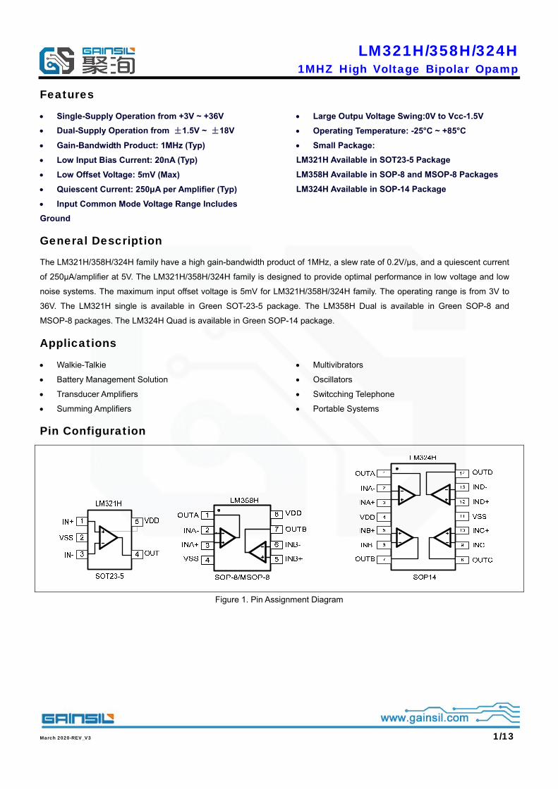
Pin Configuration
Figure 1. Pin Assignment Diagram
LM321H/358H/324H
January 2021-REV_V0 2/13
Absolute Maximum Ratings
Condition Symbol Max
Power Supply Voltage Vcc ±20V or 40V
Differential input voltage VI(DIFF) 40V
Input Voltage VI -0.3V~40V
Operating Temperature Range Topr -25°C ~+85°C
Storage Temperature Range Tstg -65°C ~+150°C
Note: Stress greater than those listed under Absolute Maximum Ratings may cause permanent damage to the device. This is a
stress rating only and functional operation of the device at these or any other conditions outside those indicated in the operational
sections of this specification are not implied. Exposure to absolute maximum rating conditions for extended periods may affect
reliability.
Package/Ordering Information
MODEL CHANNEL ORDER NUMBER PACKAGE
DESCRIPTION
PACKAGE
OPTION
MARKING
INFORMATION
LM321H Single LM321H-TR SOT23-5 Tape and Reel,3000 LM321
LM358H Dual LM358H-SR SOP-8 Tape and Reel,4000 LM358
LM358H-MR MSOP-8 Tape and Reel,3000 LM358
LM324H Quad LM324H-SR SOP-14 Tape and Reel,2500 LM324
LM321H/358H/324H
January 2021-REV_V0 3/13
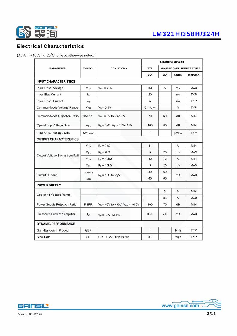
Electrical Characteristics
(At VS = +15V, TA=25oC, unless otherwise noted.)
PARAMETER SYMBOL CONDITIONS
LM321H/358H/324H
TYP MIN/MAX OVER TEMPERATURE
+25℃ +25℃ UNITS MIN/MAX
INPUT CHARACTERISTICS
Input Offset Voltage VOS VCM = VS/2 0.4 5 mV MAX
Input Bias Current IB 20 nA TYP
Input Offset Current IOS 5 nA TYP
Common-Mode Voltage Range VCM VS = 5.5V -0.1 to +4 V TYP
Common-Mode Rejection Ratio CMRR VCM = 0V to Vs-1.5V 70 60 dB MIN
Open-Loop Voltage Gain AOL RL = 5kΩ, VO = 1V to 11V 100 85 dB MIN
Input Offset Voltage Drift ΔVOS/ΔT 7 μV/℃ TYP
OUTPUT CHARACTERISTICS
Output Voltage Swing from Rail
VOH RL = 2kΩ 11 V MIN
VOL RL = 2kΩ 5 20 mV MAX
VOH RL = 10kΩ 12 13 V MIN
VOL RL = 10kΩ 5 20 mV MAX
Output Current ISOURCE
RL = 10Ω to VS/2 40 60
mA MAX ISINK 40 60
POWER SUPPLY
Operating Voltage Range 3 V MIN
36 V MAX
Power Supply Rejection Ratio PSRR VS = +5V to +36V, VCM = +0.5V 100 70 dB MIN
Quiescent Current / Amplifier IQ VS = 36V, RL=∞ 0.25 2.0 mA MAX
DYNAMIC PERFORMANCE
Gain-Bandwidth Product GBP 1 MHz TYP
Slew Rate SR G = +1, 2V Output Step 0.2 V/μs TYP
LM321H/358H/324H
January 2021-REV_V0 4/13
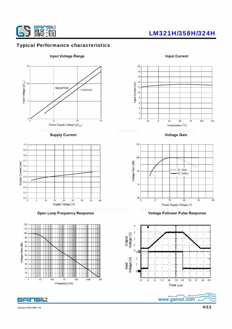
Typical Performance characteristics
LM321H/358H/324H
January 2021-REV_V0 5/13
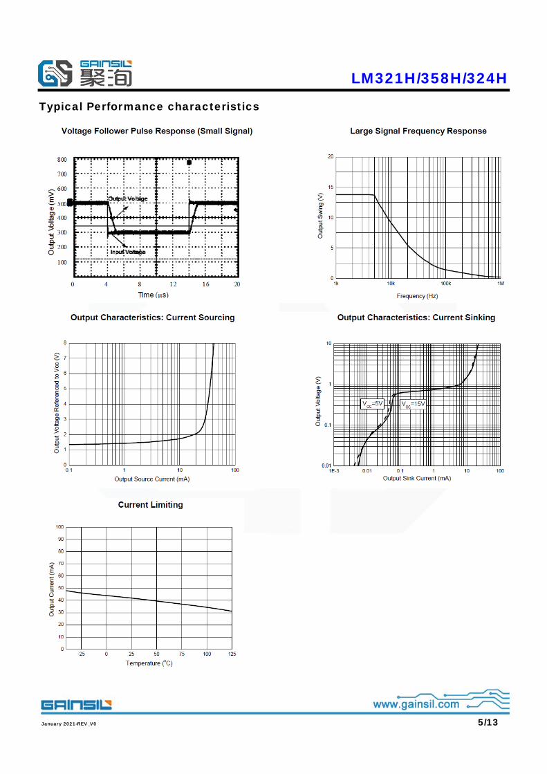
Typical Performance characteristics
LM321H/358H/324H
January 2021-REV_V0 6/13
Application Note
Size LM321H/358H/324H family series op amps are unity-gain stable and suitable for a wide range of general-purpose applications.
The small footprints of the LM321H/358H/324H family packages save space on printed circuit boards and enable the design of
smaller electronic products.
Power Supply Bypassing and Board Layout LM321H/358H/324H family series operates from a single 3V to 36V supply or dual ±1.5V to ±18V supplies. For best
performance, a 0.1μF ceramic capacitor should be placed close to the VDD pin in single supply operation. For dual supply
operation, both VDD and VSS supplies should be bypassed to ground with separate 0.1μF ceramic capacitors.
Low Supply Current The low supply current (typical 250μA per channel) of LM321H/358H/324H family will help to maximize battery life.
Operating Voltage LM321H/358H/324H family operates under wide input supply voltage (3V to 36V). In addition, all temperature specifications
apply from -25 oC to +85 oC. Most behavior remains unchanged throughout the full operating voltage range. These guarantees
ensure operation throughout the single Li-Ion battery lifetime.
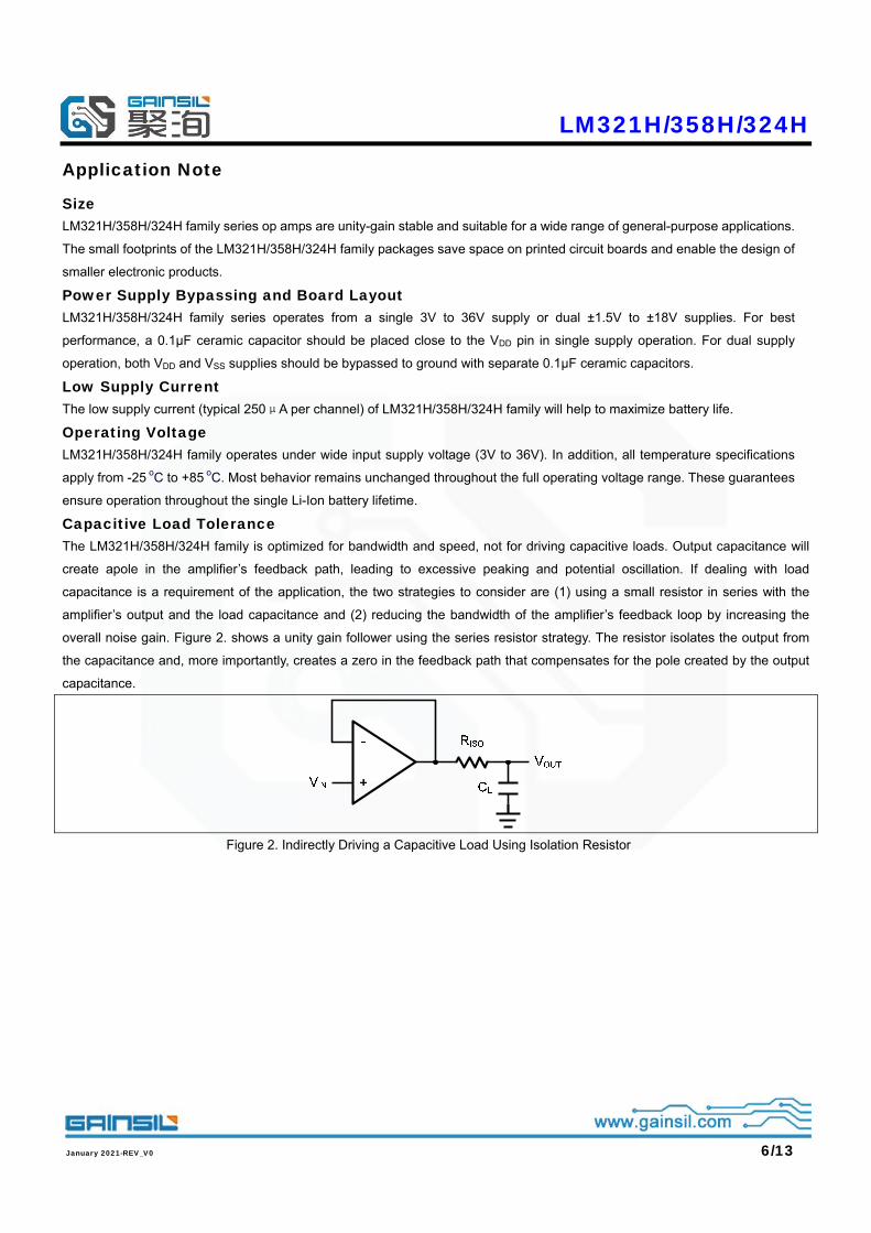
Capacitive Load Tolerance The LM321H/358H/324H family is optimized for bandwidth and speed, not for driving capacitive loads. Output capacitance will
create apole in the amplifier’s feedback path, leading to excessive peaking and potential oscillation. If dealing with load
capacitance is a requirement of the application, the two strategies to consider are (1) using a small resistor in series with the
amplifier’s output and the load capacitance and (2) reducing the bandwidth of the amplifier’s feedback loop by increasing the
overall noise gain. Figure 2. shows a unity gain follower using the series resistor strategy. The resistor isolates the output from
the capacitance and, more importantly, creates a zero in the feedback path that compensates for the pole created by the output
capacitance.
Figure 2. Indirectly Driving a Capacitive Load Using Isolation Resistor
LM321H/358H/324H
January 2021-REV_V0 7/13
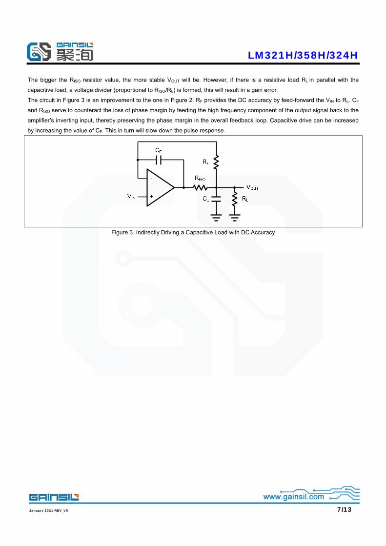
The bigger the RISO resistor value, the more stable VOUT will be. However, if there is a resistive load RL in parallel with the
capacitive load, a voltage divider (proportional to RISO/RL) is formed, this will result in a gain error.
The circuit in Figure 3 is an improvement to the one in Figure 2. RF provides the DC accuracy by feed-forward the VIN to RL. CF
and RISO serve to counteract the loss of phase margin by feeding the high frequency component of the output signal back to the
amplifier’s inverting input, thereby preserving the phase margin in the overall feedback loop. Capacitive drive can be increased
by increasing the value of CF. This in turn will slow down the pulse response.
Figure 3. Indirectly Driving a Capacitive Load with DC Accuracy
LM321H/358H/324H
January 2021-REV_V0 8/13
Typical Application Circuits
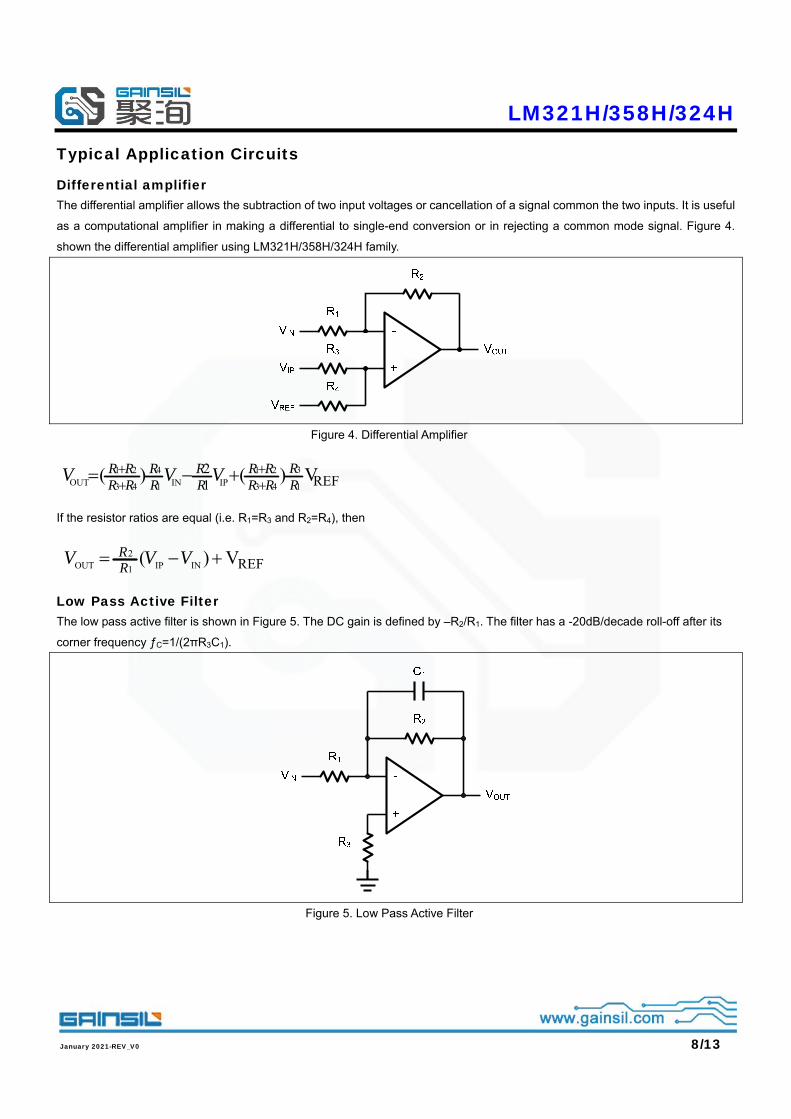
Differential amplifier The differential amplifier allows the subtraction of two input voltages or cancellation of a signal common the two inputs. It is useful
as a computational amplifier in making a differential to single-end conversion or in rejecting a common mode signal. Figure 4. shown the differential amplifier using LM321H/358H/324H family.
Figure 4. Differential Amplifier
REF12 V)()(
1
3
43
21IPIN1
4
43
21OUT R
RRRRR
RR
RR
RRRR VVV
If the resistor ratios are equal (i.e. R1=R3 and R2=R4), then
REFV)( INIP1
2OUT VVV
RR
Low Pass Active Filter The low pass active filter is shown in Figure 5. The DC gain is defined by –R2/R1. The filter has a -20dB/decade roll-off after its
corner frequency ƒC=1/(2πR3C1).
Figure 5. Low Pass Active Filter
LM321H/358H/324H
January 2021-REV_V0 9/13
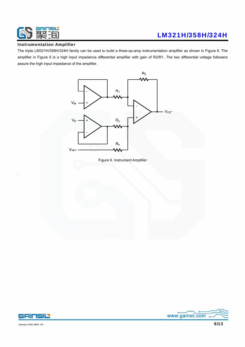
Instrumentation Amplifier The triple LM321H/358H/324H family can be used to build a three-op-amp instrumentation amplifier as shown in Figure 6. The
amplifier in Figure 6 is a high input impedance differential amplifier with gain of R2/R1. The two differential voltage followers
assure the high input impedance of the amplifier.
Figure 6. Instrument Amplifier
.
LM321H/358H/324H
January 2021-REV_V0 10/13
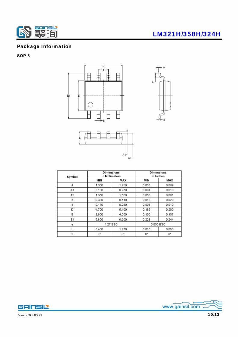
Package Information
SOP-8
LM321H/358H/324H
January 2021-REV_V0 11/13
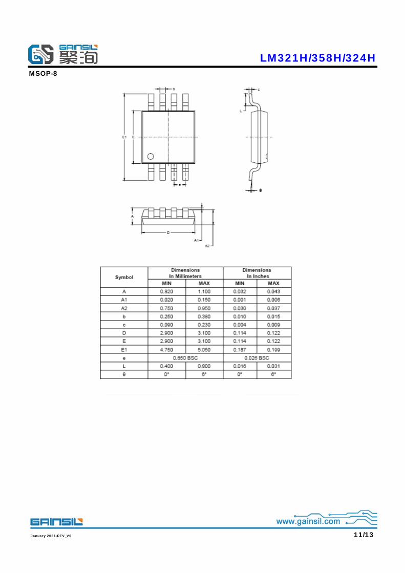
MSOP-8
LM321H/358H/324H
January 2021-REV_V0 12/13
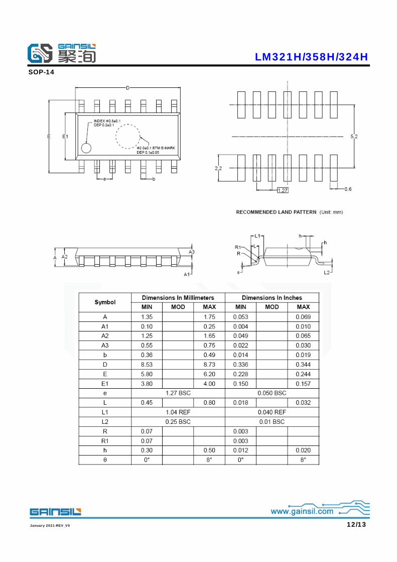
SOP-14
LM321H/358H/324H
January 2021-REV_V0 13/13
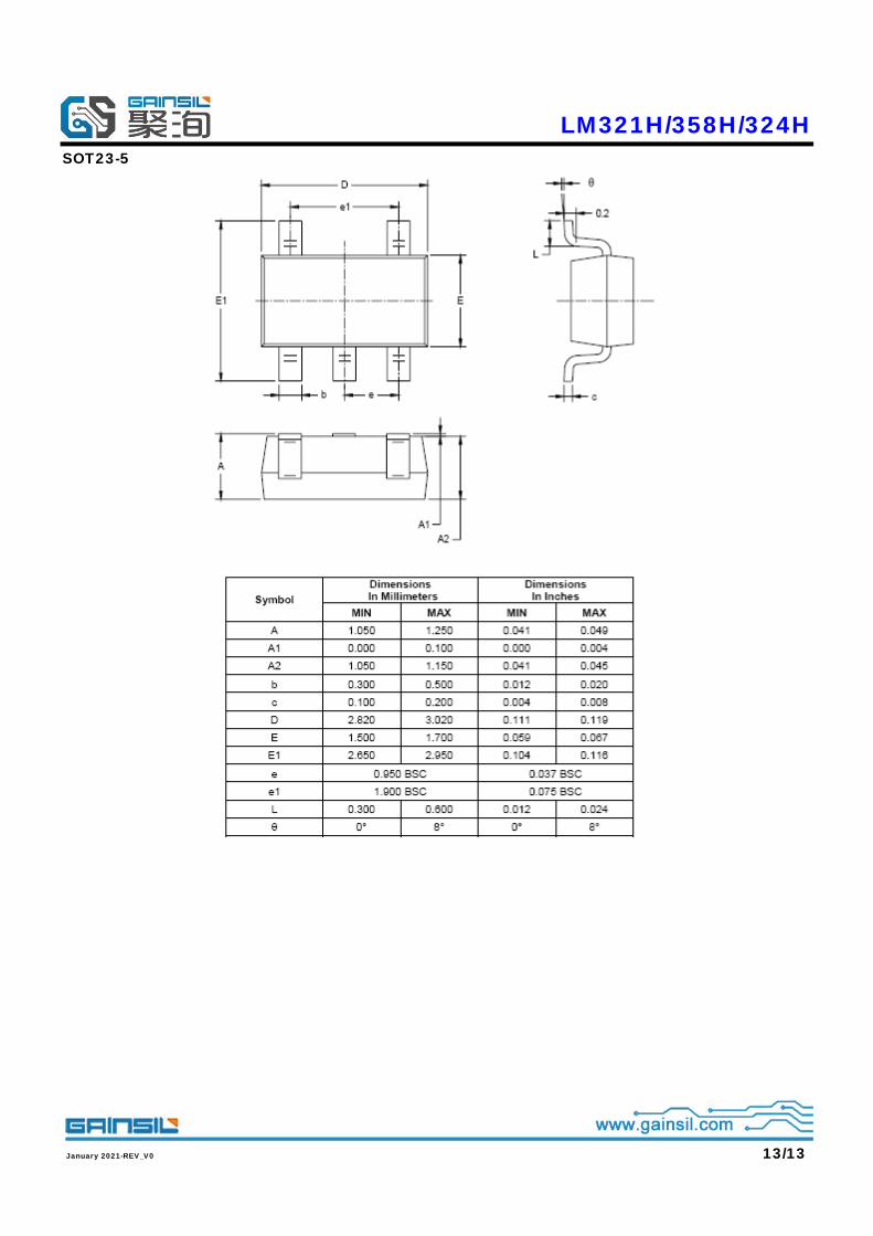
SOT23-5