新型大尺寸电磁驱动 光学扫描镜的研制 - JOS新型大尺寸电磁 驱动犕犈犕犛光学扫描镜的研制 穆参军1 ,2 张飞岭3 吴亚明1 ... 驱动方式、高的驱动效率,以及与犕犈犕犛工艺良好的兼
Product
Folder
Sample &Buy
Technical
Documents
Tools &
Software
Support &Community
英語版のTI製品についての情報を翻訳したこの資料は、製品の概要を確認する目的で便宜的に提供しているものです。該当する正式な英語版の最新情報は、www.ti.comで閲覧でき、その内容が常に優先されます。TIでは翻訳の正確性および妥当性につきましては一切保証いたしません。実際の設計などの前には、必ず最新版の英語版をご参照くださいますようお願いいたします。
English Data Sheet: SNVS036
LM2670JAJS639K –APRIL 2000–REVISED JUNE 2016
参参考考資資料料
LM2670 SIMPLE SWITCHER®高高効効率率3A降降圧圧型型電電圧圧レレギギュュレレーータタ(同同期期機機能能付付きき)
1
1 特特長長1• 最大効率94%• 標準品の外付け部品を使用して単純かつ簡単に設
計可能• 150mΩ DMOS出力スイッチ• 3.3V、5V、12Vの固定出力タイプと、可変出力
(1.2V~37V)タイプ• 電源オフのときスタンバイ電流50μA• ラインおよび負荷条件の全域において±2%の最大
出力許容誤差• 広い入力電圧範囲: 8V~40V• 外部同期クロック性能
(280kHz~400kHz)• 260kHz固定周波数の自己発振器• 動作時の接合部温度範囲: -40~125
2 アアププリリケケーーシショョンン• 設計が簡単で高効率(90%超)の降圧型スイッチン
グ・レギュレータ• リニア・レギュレータ用の効率的なシステム・プ
リレギュレータ• バッテリ・チャージャ• 同期したクロック周波数を持つ通信および無線機
器レギュレータ
3 概概要要LM2670シリーズのレギュレータはモノリシックな集積回路
で、降圧型(バック)スイッチング・レギュレータのすべての
アクティブ機能が搭載されており、優れたラインおよび負
荷レギュレーション特性で3Aまでの負荷を駆動できます。
低オン抵抗のDMOSパワー・スイッチを使用して、高い効
率(90%超)を実現しています。このシリーズには、3.3V、5V、12Vの固定出力電圧のバージョンがあります。
SIMPLE SWITCHER®コンセプトにより、最小限の外付け
部品で完全な設計を作成できます。スイッチング・クロック
周波数は内蔵の固定周波数発振器(260kHz)、または
280kHz~400kHzの範囲内の外部クロックから供給でき、
物理的に小さな部品を使用できます。LM2670で使用す
る標準インダクタは、いくつかの製造元から入手可能で、
設計プロセスを大幅に簡素化できます。外部の同期クロッ
クにより、出力リップル周波数を直接かつ正確に制御で
き、一貫したフィルタリングや周波数スペクトラムの位置決
めが可能です。
また、LM2670にはサーマル・シャットダウン、電流制限、
およびオン/オフ制御入力が組み込まれており、レギュレー
タの電源をオフして静止電流が50μAと低いスタンバイ状
態へ移行できます。出力電圧の定格許容誤差は±2%が
保証されています。
製製品品情情報報(1)
型型番番 パパッッケケーージジ 本本体体ササイイズズ(公公称称)
LM2670TO-263 (7) 10.10mm×8.89mmTO-220 (7) 14.986mm×10.16mmVSON (14) 6.00mm×5.00mm
(1) 提供されているすべてのパッケージについては、巻末の注文情報を参照してください。
代代表表的的ななアアププリリケケーーシショョンン
2
LM2670JAJS639K –APRIL 2000–REVISED JUNE 2016 www.ti.com
Copyright © 2000–2016, Texas Instruments Incorporated
目目次次1 特特長長.......................................................................... 12 アアププリリケケーーシショョンン ......................................................... 13 概概要要.......................................................................... 14 改改訂訂履履歴歴................................................................... 25 Pin Configuration and Functions ......................... 36 Specifications......................................................... 4
6.1 Absolute Maximum Ratings ...................................... 46.2 ESD Ratings.............................................................. 46.3 Recommended Operating Conditions....................... 46.4 Thermal Information .................................................. 56.5 Electrical Characteristics – 3.3 V .............................. 56.6 Electrical Characteristics – 5 V ................................. 56.7 Electrical Characteristics – 12 V ............................... 66.8 Electrical Characteristics – All Output Voltage
Versions ..................................................................... 66.9 Typical Characteristics .............................................. 7
7 Detailed Description ............................................ 107.1 Overview ................................................................. 107.2 Functional Block Diagram ....................................... 10
7.3 Feature Description................................................. 107.4 Device Functional Modes........................................ 12
8 Application and Implementation ........................ 138.1 Application Information............................................ 138.2 Typical Applications ................................................ 16
9 Power Supply Recommendations ...................... 2610 Layout................................................................... 27
10.1 Layout Guidelines ................................................. 2710.2 Layout Example .................................................... 28
11 デデババイイススおおよよびびドドキキュュメメンントトののササポポーートト ....................... 2911.1 デバイス・サポート ................................................... 2911.2 関連資料 ................................................................ 2911.3 ドキュメントの更新通知を受け取る方法..................... 2911.4 コミュニティ・リソース ................................................ 2911.5 商標 ....................................................................... 2911.6 静電気放電に関する注意事項 ................................ 2911.7 Glossary ................................................................ 29
12 メメカカニニカカルル、、パパッッケケーージジ、、おおよよびび注注文文情情報報 ................. 2912.1 DAP (VSONパッケージ) ......................................... 29
4 改改訂訂履履歴歴資料番号末尾の英字は改訂を表しています。その改訂履歴は英語版に準じています。
Revision J (April 2013) かからら Revision K にに変変更更 Page
• 「ESD定格」の表、「機能説明」セクション、「デバイスの機能モード」セクション、「アプリケーションと実装」セクション、「電源に関する推奨事項」セクション、「レイアウト」セクション、「デバイスおよびドキュメントのサポート」セクション、「メカニカル、パッケージ、および注文情報」セクションを追加 ....................................................................................................................................... 1
• 設計ソフトウェアLM267X Made Simple (バージョン 6.0)に関する記述をすべて削除................................................................. 1
Revision I (April 2013) かからら Revision J にに変変更更 Page
• Changed layout of National Data Sheet to TI format ........................................................................................................... 26
Not to scale
DAP
1NC 14 Switch_output
2Input 13 Switch_output
3Input 12 Switch_output
4CBOOST/CB 11 NC
5NC 10 NC
6SYNC 9 GND
7Feedback/FB 8 ON/OFF
Not to scale
ThermalPad
1S
witch
_o
utp
ut
2In
pu
t
3C
BO
OS
T/C
B
4G
ND
5S
YN
C
6F
ee
db
ack/F
B
7O
N/O
FF
1 Switch_output
2 Input
3 CBOOST/CB
4 GND
5 SYNC
6 Feedback/FB
7 ON/OFF
Not to scale
3
LM2670www.ti.com JAJS639K –APRIL 2000–REVISED JUNE 2016
Copyright © 2000–2016, Texas Instruments Incorporated
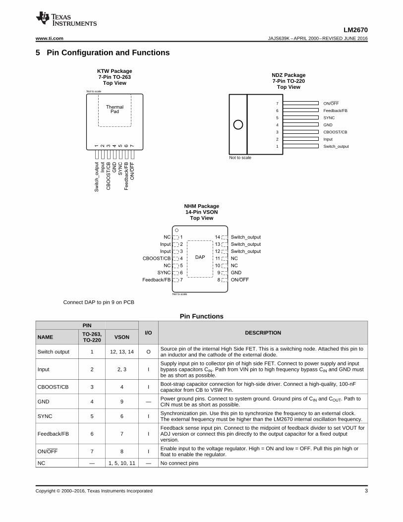
5 Pin Configuration and Functions
KTW Package7-Pin TO-263
Top ViewNDZ Package7-Pin TO-220
Top View
NHM Package14-Pin VSON
Top View
Connect DAP to pin 9 on PCB
Pin FunctionsPIN
I/O DESCRIPTIONNAME TO-263,
TO-220 VSON
Switch output 1 12, 13, 14 O Source pin of the internal High Side FET. This is a switching node. Attached this pin toan inductor and the cathode of the external diode.
Input 2 2, 3 ISupply input pin to collector pin of high side FET. Connect to power supply and inputbypass capacitors CIN. Path from VIN pin to high frequency bypass CIN and GND mustbe as short as possible.
CBOOST/CB 3 4 I Boot-strap capacitor connection for high-side driver. Connect a high-quality, 100-nFcapacitor from CB to VSW Pin.
GND 4 9 — Power ground pins. Connect to system ground. Ground pins of CIN and COUT. Path toCIN must be as short as possible.
SYNC 5 6 I Synchronization pin. Use this pin to synchronize the frequency to an external clock.The external frequency must be higher than the LM2670 internal oscillation frequency.
Feedback/FB 6 7 IFeedback sense input pin. Connect to the midpoint of feedback divider to set VOUT forADJ version or connect this pin directly to the output capacitor for a fixed outputversion.
ON/OFF 7 8 I Enable input to the voltage regulator. High = ON and low = OFF. Pull this pin high orfloat to enable the regulator.
NC — 1, 5, 10, 11 — No connect pins
4
LM2670JAJS639K –APRIL 2000–REVISED JUNE 2016 www.ti.com
Copyright © 2000–2016, Texas Instruments Incorporated
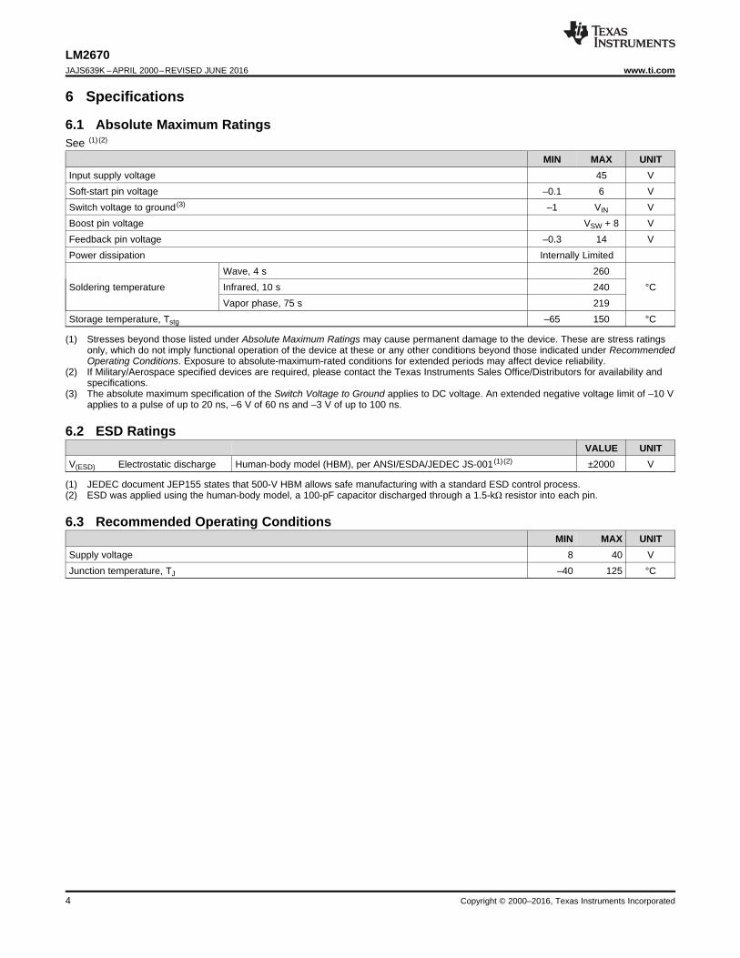
(1) Stresses beyond those listed under Absolute Maximum Ratings may cause permanent damage to the device. These are stress ratingsonly, which do not imply functional operation of the device at these or any other conditions beyond those indicated under RecommendedOperating Conditions. Exposure to absolute-maximum-rated conditions for extended periods may affect device reliability.
(2) If Military/Aerospace specified devices are required, please contact the Texas Instruments Sales Office/Distributors for availability andspecifications.
(3) The absolute maximum specification of the Switch Voltage to Ground applies to DC voltage. An extended negative voltage limit of –10 Vapplies to a pulse of up to 20 ns, –6 V of 60 ns and –3 V of up to 100 ns.
6 Specifications
6.1 Absolute Maximum RatingsSee (1) (2)
MIN MAX UNITInput supply voltage 45 VSoft-start pin voltage –0.1 6 VSwitch voltage to ground (3) –1 VIN VBoost pin voltage VSW + 8 VFeedback pin voltage –0.3 14 VPower dissipation Internally Limited
Soldering temperatureWave, 4 s 260
°CInfrared, 10 s 240Vapor phase, 75 s 219
Storage temperature, Tstg –65 150 °C
(1) JEDEC document JEP155 states that 500-V HBM allows safe manufacturing with a standard ESD control process.(2) ESD was applied using the human-body model, a 100-pF capacitor discharged through a 1.5-kΩ resistor into each pin.
6.2 ESD RatingsVALUE UNIT
V(ESD) Electrostatic discharge Human-body model (HBM), per ANSI/ESDA/JEDEC JS-001 (1) (2) ±2000 V
6.3 Recommended Operating ConditionsMIN MAX UNIT
Supply voltage 8 40 VJunction temperature, TJ –40 125 °C
5
LM2670www.ti.com JAJS639K –APRIL 2000–REVISED JUNE 2016
Copyright © 2000–2016, Texas Instruments Incorporated
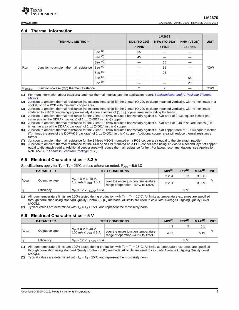
(1) For more information about traditional and new thermal metrics, see the application report, Semiconductor and IC Package ThermalMetrics.
(2) Junction to ambient thermal resistance (no external heat sink) for the 7-lead TO-220 package mounted vertically, with ½ inch leads in asocket, or on a PCB with minimum copper area.
(3) Junction to ambient thermal resistance (no external heat sink) for the 7-lead TO-220 package mounted vertically, with ½ inch leadssoldered to a PCB containing approximately 4 square inches of (1 oz.) copper area surrounding the leads.
(4) Junction to ambient thermal resistance for the 7-lead DDPAK mounted horizontally against a PCB area of 0.136 square inches (thesame size as the DDPAK package) of 1 oz (0.0014 in thick) copper.
(5) Junction to ambient thermal resistance for the 7-lead DDPAK mounted horizontally against a PCB area of 0.4896 square inches (3.6times the area of the DDPAK package) of 1 oz (0.0014 in thick) copper.
(6) Junction to ambient thermal resistance for the 7-lead DDPAK mounted horizontally against a PCB copper area of 1.0064 square inches(7.4 times the area of the DDPAK 3 package) of 1 oz (0.0014 in thick) copper. Additional copper area will reduce thermal resistancefurther.
(7) Junction to ambient thermal resistance for the 14-lead VSON mounted on a PCB copper area equal to the die attach paddle.(8) Junction to ambient thermal resistance for the 14-lead VSON mounted on a PCB copper area using 12 vias to a second layer of copper
equal to die attach paddle. Additional copper area will reduce thermal resistance further. For layout recommendations, see ApplicationNote AN-1187 Leadless Leadfram Package (LLP).
6.4 Thermal Information
THERMAL METRIC (1)LM2678
UNITNDZ (TO-220) KTW (TO-263) NHM (VSON)7 PINS 7 PINS 14 PINS
RθJA Junction-to-ambient thermal resistance
See (2) 65 — —
°C/W
See (3) 45 — —See (4) — 56 —See (5) — 35 —See (6) — 26 —See (7) — — 55See (8) — — 29
RθJC(top) Junction-to-case (top) thermal resistance 2 2 — °C/W
(1) All room temperature limits are 100% tested during production with TA = TJ = 25°C. All limits at temperature extremes are specifiedthrough correlation using standard Quality Control (SQC) methods. All limits are used to calculate Average Outgoing Quality Level(AOQL).
(2) Typical values are determined with TA = TJ = 25°C and represent the most likely norm.
6.5 Electrical Characteristics – 3.3 VSpecifications apply for TA = TJ = 25°C unless otherwise noted. RADJ = 5.6 kΩ.
PARAMETER TEST CONDITIONS MIN (1) TYP (2) MAX (1) UNIT
VOUT Output voltage VIN = 8 V to 40 V,100 mA ≤ IOUT ≤ 5 A
3.234 3.3 3.366Vover the entire junction temperature
range of operation –40°C to 125°C 3.201 3.399
η Efficiency VIN = 12 V, ILOAD = 5 A 86%
(1) All room temperature limits are 100% tested during production with TA = TJ = 25°C. All limits at temperature extremes are specifiedthrough correlation using standard Quality Control (SQC) methods. All limits are used to calculate Average Outgoing Quality Level(AOQL).
(2) Typical values are determined with TA = TJ = 25°C and represent the most likely norm.
6.6 Electrical Characteristics – 5 VPARAMETER TEST CONDITIONS MIN (1) TYP (2) MAX (1) UNIT
VOUT Output voltage VIN = 8 V to 40 V,100 mA ≤ IOUT ≤ 5 A
4.9 5 5.1Vover the entire junction temperature
range of operation –40°C to 125°C 4.85 5.15
η Efficiency VIN = 12 V, ILOAD = 5 A 88%
6
LM2670JAJS639K –APRIL 2000–REVISED JUNE 2016 www.ti.com
Copyright © 2000–2016, Texas Instruments Incorporated
(1) All room temperature limits are 100% tested during production with TA = TJ = 25°C. All limits at temperature extremes are specifiedthrough correlation using standard Quality Control (SQC) methods. All limits are used to calculate Average Outgoing Quality Level(AOQL).
(2) Typical values are determined with TA = TJ = 25°C and represent the most likely norm.
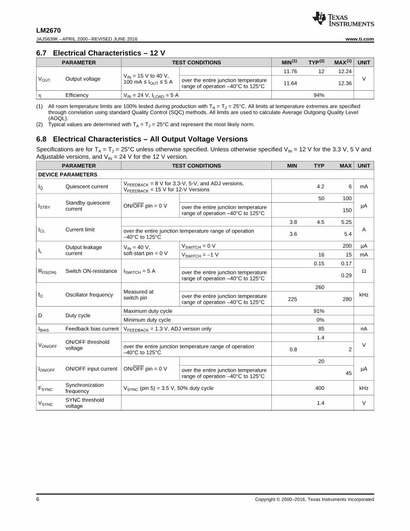
6.7 Electrical Characteristics – 12 VPARAMETER TEST CONDITIONS MIN (1) TYP (2) MAX (1) UNIT
VOUT Output voltage VIN = 15 V to 40 V,100 mA ≤ IOUT ≤ 5 A
11.76 12 12.24Vover the entire junction temperature
range of operation –40°C to 125°C 11.64 12.36
η Efficiency VIN = 24 V, ILOAD = 5 A 94%
6.8 Electrical Characteristics – All Output Voltage VersionsSpecifications are for TA = TJ = 25°C unless otherwise specified. Unless otherwise specified VIN = 12 V for the 3.3 V, 5 V andAdjustable versions, and VIN = 24 V for the 12 V version.
PARAMETER TEST CONDITIONS MIN TYP MAX UNITDEVICE PARAMETERS
IQ Quiescent current VFEEDBACK = 8 V for 3.3-V, 5-V, and ADJ versions,VFEEDBACK = 15 V for 12-V Versions 4.2 6 mA
ISTBYStandby quiescentcurrent ON/OFF pin = 0 V
50 100µAover the entire junction temperature
range of operation –40°C to 125°C 150
ICL Current limit3.8 4.5 5.25
Aover the entire junction temperature range of operation–40°C to 125°C 3.6 5.4
ILOutput leakagecurrent
VIN = 40 V,soft-start pin = 0 V
VSWITCH = 0 V 200 µAVSWITCH = –1 V 16 15 mA
RDS(ON) Switch ON-resistance ISWITCH = 5 A0.15 0.17
Ωover the entire junction temperaturerange of operation –40°C to 125°C 0.29
fO Oscillator frequency Measured atswitch pin
260kHzover the entire junction temperature
range of operation –40°C to 125°C 225 280
D Duty cycleMaximum duty cycle 91%Minimum duty cycle 0%
IBIAS Feedback bias current VFEEDBACK = 1.3 V, ADJ version only 85 nA
VON/OFFON/OFF thresholdvoltage
1.4Vover the entire junction temperature range of operation
–40°C to 125°C 0.8 2
ION/OFF ON/OFF input current ON/OFF pin = 0 V20
µAover the entire junction temperaturerange of operation –40°C to 125°C 45
FSYNCSynchronizationfrequency VSYNC (pin 5) = 3.5 V, 50% duty cycle 400 kHz
VSYNCSYNC thresholdvoltage 1.4 V
7
LM2670www.ti.com JAJS639K –APRIL 2000–REVISED JUNE 2016
Copyright © 2000–2016, Texas Instruments Incorporated
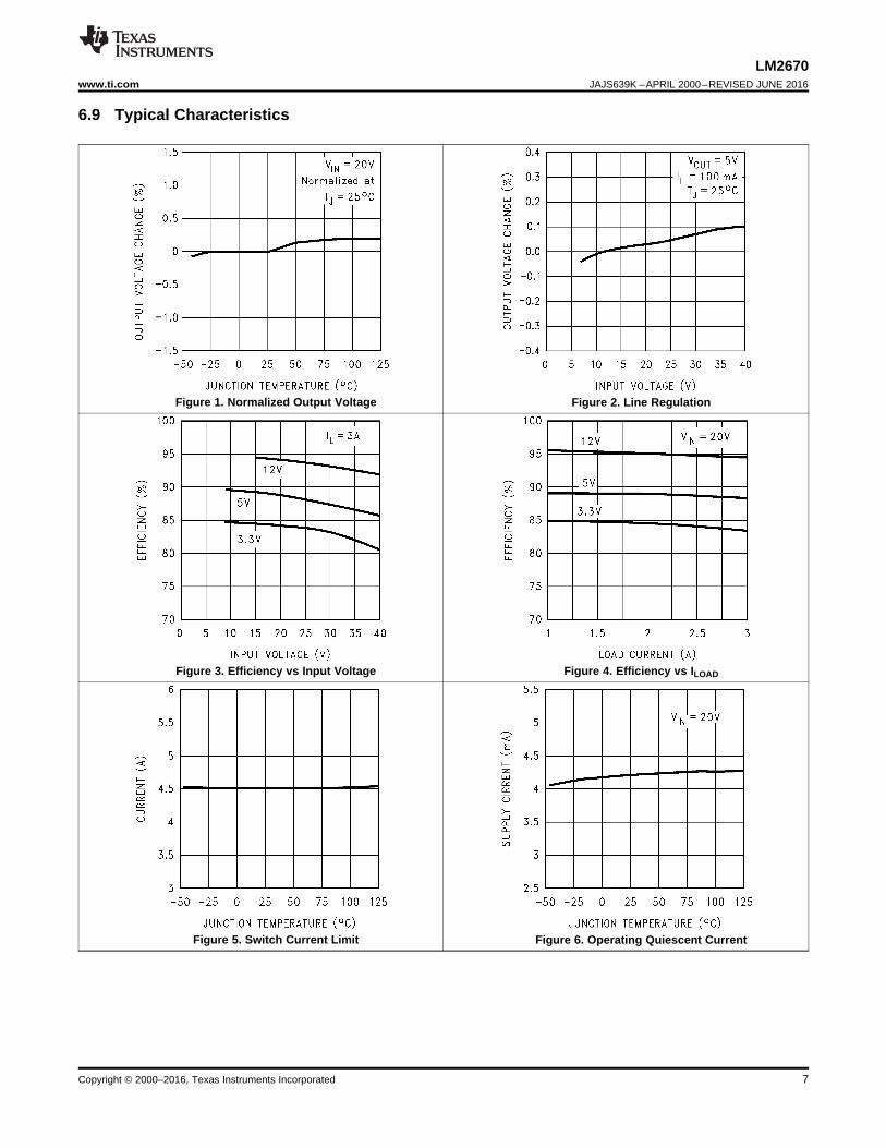
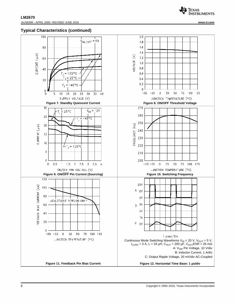
6.9 Typical Characteristics
Figure 1. Normalized Output Voltage Figure 2. Line Regulation
Figure 3. Efficiency vs Input Voltage Figure 4. Efficiency vs ILOAD
Figure 5. Switch Current Limit Figure 6. Operating Quiescent Current
8
LM2670JAJS639K –APRIL 2000–REVISED JUNE 2016 www.ti.com
Copyright © 2000–2016, Texas Instruments Incorporated
Typical Characteristics (continued)
Figure 7. Standby Quiescent Current Figure 8. ON/OFF Threshold Voltage
Figure 9. ON/OFF Pin Current (Sourcing) Figure 10. Switching Frequency
Figure 11. Feedback Pin Bias Current
Continuous Mode Switching Waveforms VIN = 20 V, VOUT = 5 V,ILOAD = 3 A, L = 33 µH, COUT = 200 µF, COUTESR = 26 mΩ
A: VSW Pin Voltage, 10 V/divB: Inductor Current, 1 A/div
C: Output Ripple Voltage, 20 mV/div AC-Coupled
Figure 12. Horizontal Time Base: 1 µs/div
9
LM2670www.ti.com JAJS639K –APRIL 2000–REVISED JUNE 2016
Copyright © 2000–2016, Texas Instruments Incorporated
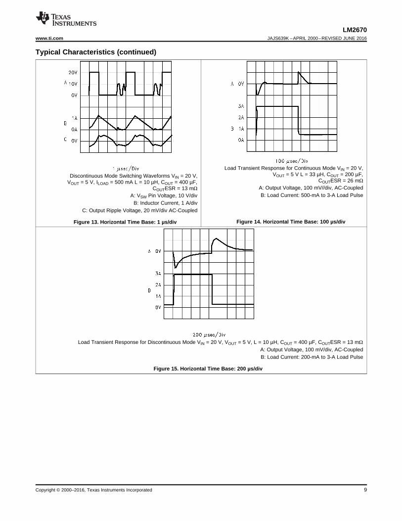
Typical Characteristics (continued)
Discontinuous Mode Switching Waveforms VIN = 20 V,VOUT = 5 V, ILOAD = 500 mA L = 10 µH, COUT = 400 µF,
COUTESR = 13 mΩA: VSW Pin Voltage, 10 V/div
B: Inductor Current, 1 A/divC: Output Ripple Voltage, 20 mV/div AC-Coupled
Figure 13. Horizontal Time Base: 1 µs/div
Load Transient Response for Continuous Mode VIN = 20 V,VOUT = 5 V L = 33 µH, COUT = 200 µF,
COUTESR = 26 mΩA: Output Voltage, 100 mV//div, AC-CoupledB: Load Current: 500-mA to 3-A Load Pulse
Figure 14. Horizontal Time Base: 100 µs/div
Load Transient Response for Discontinuous Mode VIN = 20 V, VOUT = 5 V, L = 10 µH, COUT = 400 µF, COUTESR = 13 mΩA: Output Voltage, 100 mV/div, AC-CoupledB: Load Current: 200-mA to 3-A Load Pulse
Figure 15. Horizontal Time Base: 200 µs/div
10
LM2670JAJS639K –APRIL 2000–REVISED JUNE 2016 www.ti.com
Copyright © 2000–2016, Texas Instruments Incorporated
7 Detailed Description
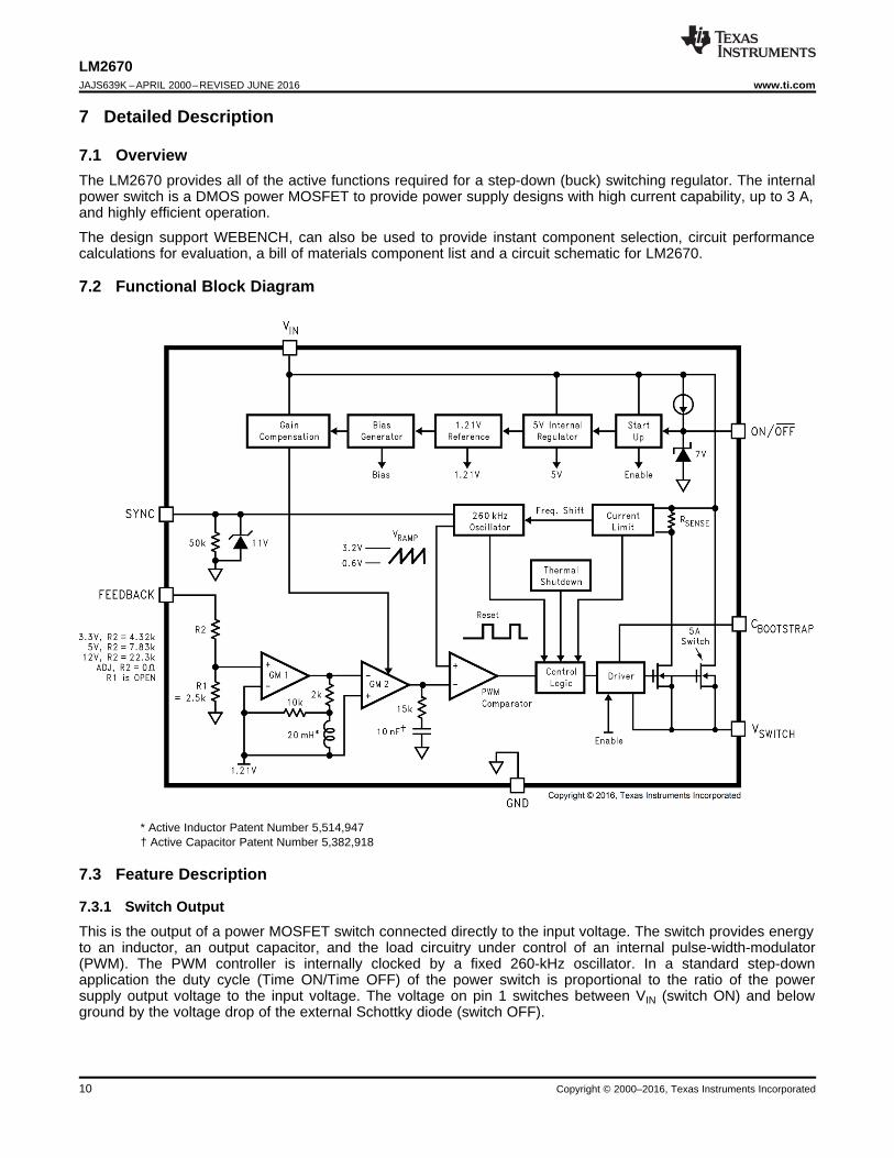
7.1 OverviewThe LM2670 provides all of the active functions required for a step-down (buck) switching regulator. The internalpower switch is a DMOS power MOSFET to provide power supply designs with high current capability, up to 3 A,and highly efficient operation.
The design support WEBENCH, can also be used to provide instant component selection, circuit performancecalculations for evaluation, a bill of materials component list and a circuit schematic for LM2670.
7.2 Functional Block Diagram
* Active Inductor Patent Number 5,514,947† Active Capacitor Patent Number 5,382,918
7.3 Feature Description
7.3.1 Switch OutputThis is the output of a power MOSFET switch connected directly to the input voltage. The switch provides energyto an inductor, an output capacitor, and the load circuitry under control of an internal pulse-width-modulator(PWM). The PWM controller is internally clocked by a fixed 260-kHz oscillator. In a standard step-downapplication the duty cycle (Time ON/Time OFF) of the power switch is proportional to the ratio of the powersupply output voltage to the input voltage. The voltage on pin 1 switches between VIN (switch ON) and belowground by the voltage drop of the external Schottky diode (switch OFF).
11
LM2670www.ti.com JAJS639K –APRIL 2000–REVISED JUNE 2016
Copyright © 2000–2016, Texas Instruments Incorporated
Feature Description (continued)7.3.2 InputThe input voltage for the power supply is connected to pin 2. In addition to providing energy to the load the inputvoltage also provides bias for the internal circuitry of the LM2670. For ensured performance the input voltagemust be in the range of 8 V to 40 V. For best performance of the power supply the input pin must always bebypassed with an input capacitor located close to pin 2.
7.3.3 C BoostA capacitor must be connected from pin 3 to the switch output, pin 1. This capacitor boosts the gate drive to theinternal MOSFET above VIN to fully turn it ON. This minimizes conduction losses in the power switch to maintainhigh efficiency. The recommended value for C Boost is 0.01 µF.
7.3.4 GroundThis is the ground reference connection for all components in the power supply. In fast-switching, high-currentapplications such as those implemented with the LM2670, TI recommends using a broad ground plane tominimize signal coupling throughout the circuit.
7.3.5 SYNCThis input allows control of the switching clock frequency. If left open-circuited the regulator will be switched atthe internal oscillator frequency, between 225 kHz and 280 kHz. An external clock can be used to force theswitching frequency and thereby control the output ripple frequency of the regulator. This capability provides forconsistent filtering of the output ripple from system to system as well as precise frequency spectrum positioningof the ripple frequency which is often desired in communications and radio applications. This external frequencymust be greater than the LM2670 internal oscillator frequency, which could be as high as 280 kHz, to prevent anerroneous reset of the internal ramp oscillator and PWM control of the power switch. The ramp oscillator is reseton the positive going edge of the sync input signal. TI recommends that the external TTL or CMOS compatibleclock (between 0 V and a level greater than 3 V) be AC-coupled to the sync input through a 100-pf capacitor anda 1-kΩ resistor to ground at pin 5 as shown in Figure 21.
When the SYNC function is used, current limit frequency foldback is not active. Therefore, the device my not befully protected against extreme output short-circuit conditions. See Additional Application Information.
7.3.6 FeedbackThis is the input to a two-stage high gain amplifier, which drives the PWM controller. It is necessary to connectpin 6 to the actual output of the power supply to set the DC output voltage. For the fixed output devices (3.3-V, 5-V, and 12-V outputs), a direct wire connection to the output is all that is required as internal gain setting resistorsare provided inside the LM2670. For the adjustable output version two external resistors are required to set theDC output voltage. For stable operation of the power supply it is important to prevent coupling of any inductorflux to the feedback input.
7.3.7 ON/OFFThis input provides an electrical ON/OFF control of the power supply. Connecting this pin to ground or to anyvoltage less than 0.8 V will completely turn OFF the regulator. The current drain from the input supply when OFFis only 50 µA. Pin 7 has an internal pull-up current source of approximately 20 µA and a protection clamp Zenerdiode of 7 V to ground. When electrically driving the ON/OFF pin the high voltage level for the ON conditionshould not exceed the 6-V absolute maximum limit. When ON/OFF control is not required pin 7 should be leftopen circuited.
12
LM2670JAJS639K –APRIL 2000–REVISED JUNE 2016 www.ti.com
Copyright © 2000–2016, Texas Instruments Incorporated
7.4 Device Functional Modes
7.4.1 Shutdown ModeThe ON/OFF pin provides electrical ON and OFF control for the LM2670. When the voltage of this pin is lowerthan 1.4 V, the device is shutdown mode. The typical standby current in this mode is 50 µA.
7.4.2 Active ModeWhen the voltage of the ON/OFF pin is higher than 1.4 V, the device starts switching and the output voltage risesuntil it reaches a normal regulation voltage.
13
LM2670www.ti.com JAJS639K –APRIL 2000–REVISED JUNE 2016
Copyright © 2000–2016, Texas Instruments Incorporated
8 Application and Implementation
NOTEInformation in the following applications sections is not part of the TI componentspecification, and TI does not warrant its accuracy or completeness. TI’s customers areresponsible for determining suitability of components for their purposes. Customers shouldvalidate and test their design implementation to confirm system functionality.
8.1 Application Information
8.1.1 Design ConsiderationsPower supply design using the LM2670 is greatly simplified by using recommended external components. A widerange of inductors, capacitors and Schottky diodes from several manufacturers have been evaluated for use indesigns that cover the full range of capabilities (input voltage, output voltage, and load current) of the LM2670. Asimple design procedure using nomographs and component tables provided in this data sheet leads to a workingdesign with very little effort.
The individual components from the various manufacturers called out for use are still just a small sample of thevast array of components available in the industry. While these components are recommended, they are notexclusively the only components for use in a design. After a close comparison of component specifications,equivalent devices from other manufacturers could be substituted for use in an application.
Important considerations for each external component and an explanation of how the nomographs and selectiontables were developed follows.
8.1.2 InductorThe inductor is the key component in a switching regulator. For efficiency the inductor stores energy during theswitch ON time and then transfers energy to the load while the switch is OFF.
Nomographs are used to select the inductance value required for a given set of operating conditions. Thenomographs assume that the circuit is operating in continuous mode (the current flowing through the inductornever falls to zero). The magnitude of inductance is selected to maintain a maximum ripple current of 30% of themaximum load current. If the ripple current exceeds this 30% limit the next larger value is selected.
The inductors offered have been specifically manufactured to provide proper operation under all operatingconditions of input and output voltage and load current. Several part types are offered for a given amount ofinductance. Both surface mount and through-hole devices are available. The inductors from each of the threemanufacturers have unique characteristics.• Renco: ferrite stick core inductors; benefits are typically lowest cost and can withstand ripple and transient
peak currents above the rated value. These inductors have an external magnetic field, which may generateEMI.
• Pulse Engineering: powdered iron toroid core inductors; these also can withstand higher than rated currentsand, being toroid inductors, have low EMI.
• Coilcraft: ferrite drum core inductors; these are the smallest physical size inductors and are available only assurface mount components. These inductors also generate EMI but less than stick inductors.
8.1.3 Output CapacitorThe output capacitor acts to smooth the DC output voltage and also provides energy storage. Selection of anoutput capacitor, with an associated equivalent series resistance (ESR), impacts both the amount of output ripplevoltage and stability of the control loop.
The output ripple voltage of the power supply is the product of the capacitor ESR and the inductor ripple current.The capacitor types recommended in the tables were selected for having low ESR ratings.
In addition, both surface mount tantalum capacitors and through-hole aluminum electrolytic capacitors are offeredas solutions.
14
LM2670JAJS639K –APRIL 2000–REVISED JUNE 2016 www.ti.com
Copyright © 2000–2016, Texas Instruments Incorporated
Application Information (continued)Impacting frequency stability of the overall control loop, the output capacitance, in conjunction with the inductor,creates a double pole inside the feedback loop. In addition the capacitance and the ESR value create a zero.These frequency response effects together with the internal frequency compensation circuitry of the LM2670modify the gain and phase shift of the closed-loop system.
As a general rule for stable switching regulator circuits it is desired to have the unity gain bandwidth of the circuitto be limited to no more than one-sixth of the controller switching frequency. With the fixed 260-kHz switchingfrequency of the LM2670, the output capacitor is selected to provide a unity gain bandwidth of 40 kHz maximum.Each recommended capacitor value has been chosen to achieve this result.
In some cases multiple capacitors are required either to reduce the ESR of the output capacitor, to minimizeoutput ripple (a ripple voltage of 1% of VOUT or less is the assumed performance condition), or to increase theoutput capacitance to reduce the closed loop unity gain bandwidth (to less than 40 kHz). When parallelcombinations of capacitors are required it has been assumed that each capacitor is the exact same part type.
The RMS current and working voltage (WV) ratings of the output capacitor are also important considerations. In atypical step-down switching regulator, the inductor ripple current (set to be no more than 30% of the maximumload current by the inductor selection) is the current that flows through the output capacitor. The capacitor RMScurrent rating must be greater than this ripple current. The voltage rating of the output capacitor must be greaterthan 1.3 times the maximum output voltage of the power supply. If operation of the system at elevatedtemperatures is required, the capacitor voltage rating may be de-rated to less than the nominal room temperaturerating. Careful inspection of the manufacturer's specification for de-rating of working voltage with temperature isimportant.
8.1.4 Input CapacitorFast changing currents in high current switching regulators place a significant dynamic load on the unregulatedpower source. An input capacitor helps to provide additional current to the power supply as well as smooth outinput voltage variations.
Like the output capacitor, the key specifications for the input capacitor are RMS current rating and workingvoltage. The RMS current flowing through the input capacitor is equal to one-half of the maximum DC loadcurrent so the capacitor should be rated to handle this. Paralleling multiple capacitors proportionally increasesthe current rating of the total capacitance. The voltage rating must also be selected to be 1.3 times the maximuminput voltage. Depending on the unregulated input power source, under light load conditions the maximum inputvoltage could be significantly higher than normal operation. Consider when selecting an input capacitor.
The input capacitor must be placed very close to the input pin of the LM2670. Due to relative high currentoperation with fast transient changes, the series inductance of input connecting wires or PCB traces can createringing signals at the input terminal which could possibly propagate to the output or other parts of the circuitry. Itmay be necessary in some designs to add a small valued (0.1 µF to 0.47 µF) ceramic type capacitor in parallelwith the input capacitor to prevent or minimize any ringing.
8.1.5 Catch DiodeWhen the power switch in the LM2670 turns OFF, the current through the inductor continues to flow. The path forthis current is through the diode connected between the switch output and ground. This forward biased diodeclamps the switch output to a voltage less than ground. This negative voltage must be greater than –1 V so a lowvoltage drop (particularly at high current levels) Schottky diode is recommended. Total efficiency of the entirepower supply is significantly impacted by the power lost in the output catch diode. The average current throughthe catch diode is dependent on the switch duty cycle (D) and is equal to the load current times (1-D). Use of adiode rated for much higher current than is required by the actual application helps to minimize the voltage dropand power loss in the diode.
During the switch ON time the diode is reversed biased by the input voltage. The reverse voltage rating of thediode must be at least 1.3 times greater than the maximum input voltage.
8.1.6 Boost CapacitorThe boost capacitor creates a voltage used to overdrive the gate of the internal power MOSFET. This improvesefficiency by minimizing the on resistance of the switch and associated power loss. For all applications, TIrecommends using a 0.01-µF, 50-V ceramic capacitor.
15
LM2670www.ti.com JAJS639K –APRIL 2000–REVISED JUNE 2016
Copyright © 2000–2016, Texas Instruments Incorporated
Application Information (continued)8.1.7 Sync ComponentsWhen synchronizing the LM2670 with an external clock it is recommended to connect the clock to pin 5 througha series 100-pf capacitor and connect a 1-kΩ resistor to ground from pin 5. This RC network creates a short 100-ns pulse on each positive edge of the clock to reset the internal ramp oscillator. The reset time of the oscillator isapproximately 300 ns.
8.1.8 Additional Application InformationWhen the output voltage is greater than approximately 6 V, and the duty cycle at minimum input voltage isgreater than approximately 50%, the designer should exercise caution in selection of the output filtercomponents. When an application designed to these specific operating conditions is subjected to a current limitfault condition, it may be possible to observe a large hysteresis in the current limit. This can affect the outputvoltage of the device until the load current is reduced sufficiently to allow the current limit protection circuit toreset itself.
Under current limiting conditions, the LM267x is designed to respond in the following manner:1. At the moment when the inductor current reaches the current limit threshold, the ON-pulse is immediately
terminated. This happens for any application condition.2. However, the current limit block is also designed to momentarily reduce the duty cycle to below 50% to avoid
subharmonic oscillations, which could cause the inductor to saturate.3. Thereafter, once the inductor current falls below the current limit threshold, there is a small relaxation time
during which the duty cycle progressively rises back above 50% to the value required to achieve regulation.
If the output capacitance is sufficiently large, it may be possible that as the output tries to recover, the outputcapacitor charging current is large enough to repeatedly re-trigger the current limit circuit before the output hasfully settled. This condition is exacerbated with higher output voltage settings because the energy requirement ofthe output capacitor varies as the square of the output voltage (½ CV2), thus requiring an increased chargingcurrent.
A simple test to determine if this condition might exist for a suspect application is to apply a short circuit acrossthe output of the converter, and then remove the shorted output condition. In an application with properlyselected external components, the output recovers smoothly.
Practical values of external components that have been experimentally found to work well under these specificoperating conditions are COUT = 47 µF, L = 22 µH. It should be noted that even with these components, for adevice’s current limit of ICLIM, the maximum load current under which the possibility of the large current limithysteresis can be minimized is ICLIM / 2. For example, if the input is 24 V and the set output voltage is 18 V, thenfor a desired maximum current of 1.5 A, the current limit of the chosen switcher must be confirmed to be at least3 A.
Under extreme overcurrent or short-circuit conditions, the LM267X employs frequency foldback in addition to thecurrent limit. If the cycle-by-cycle inductor current increases above the current limit threshold (due to short circuitor inductor saturation for example) the switching frequency is automatically reduced to protect the IC. Frequencybelow 100 kHz is typical for an extreme short-circuit condition.
16
LM2670JAJS639K –APRIL 2000–REVISED JUNE 2016 www.ti.com
Copyright © 2000–2016, Texas Instruments Incorporated
8.2 Typical Applications
8.2.1 Typical Application for All Output Voltage Versions
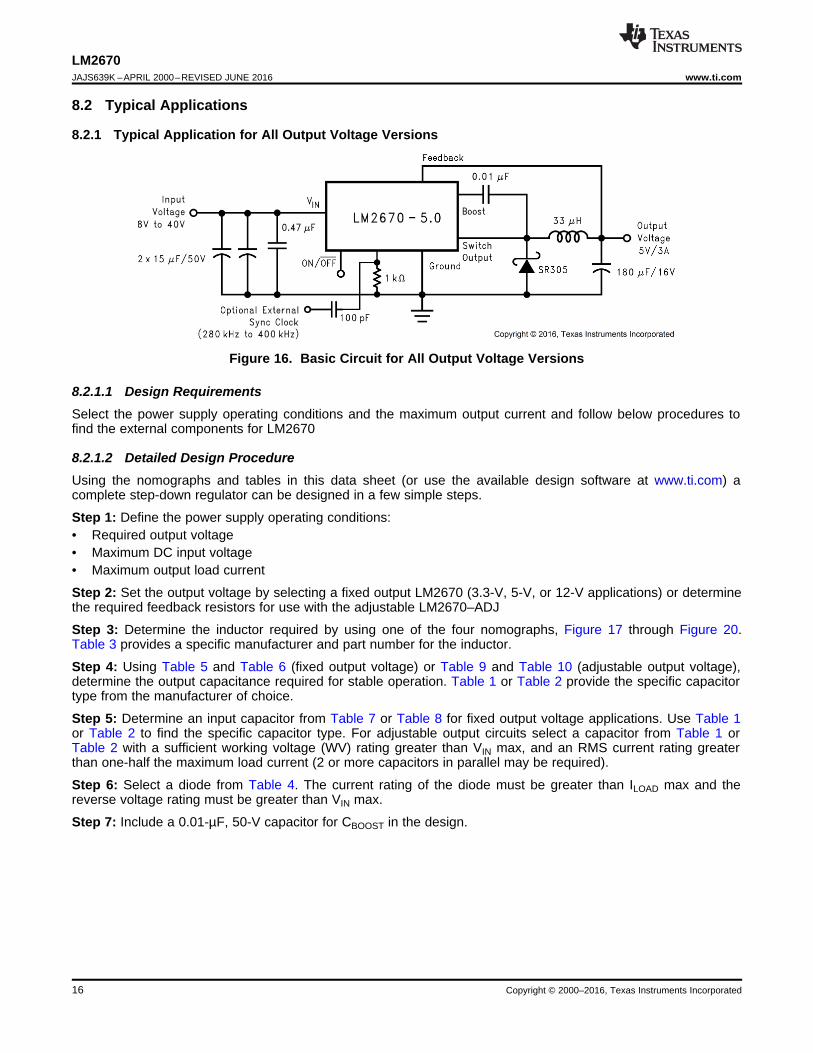
Figure 16. Basic Circuit for All Output Voltage Versions
8.2.1.1 Design RequirementsSelect the power supply operating conditions and the maximum output current and follow below procedures tofind the external components for LM2670
8.2.1.2 Detailed Design ProcedureUsing the nomographs and tables in this data sheet (or use the available design software at www.ti.com) acomplete step-down regulator can be designed in a few simple steps.
Step 1: Define the power supply operating conditions:• Required output voltage• Maximum DC input voltage• Maximum output load current
Step 2: Set the output voltage by selecting a fixed output LM2670 (3.3-V, 5-V, or 12-V applications) or determinethe required feedback resistors for use with the adjustable LM2670–ADJ
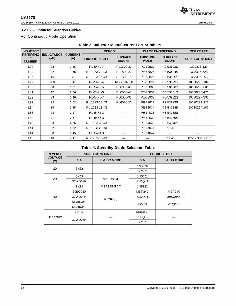
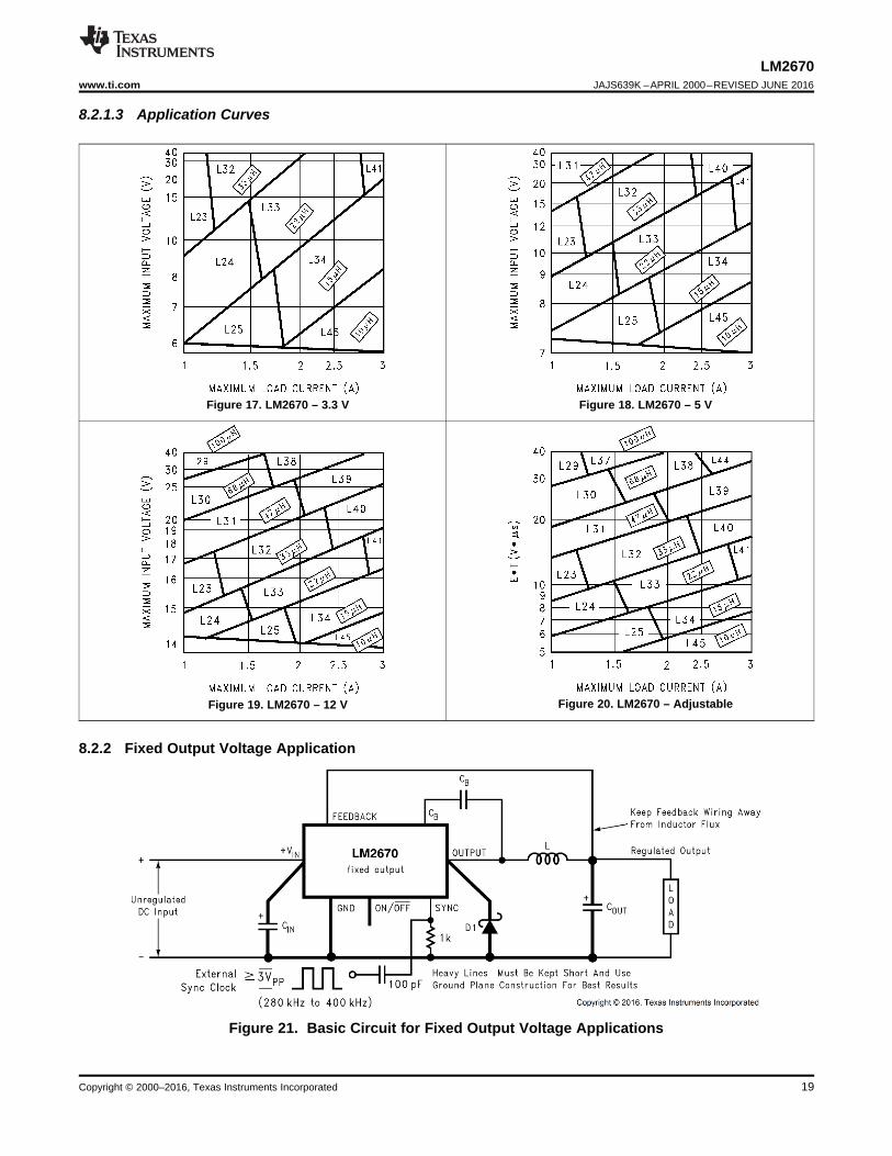
Step 3: Determine the inductor required by using one of the four nomographs, Figure 17 through Figure 20.Table 3 provides a specific manufacturer and part number for the inductor.
Step 4: Using Table 5 and Table 6 (fixed output voltage) or Table 9 and Table 10 (adjustable output voltage),determine the output capacitance required for stable operation. Table 1 or Table 2 provide the specific capacitortype from the manufacturer of choice.
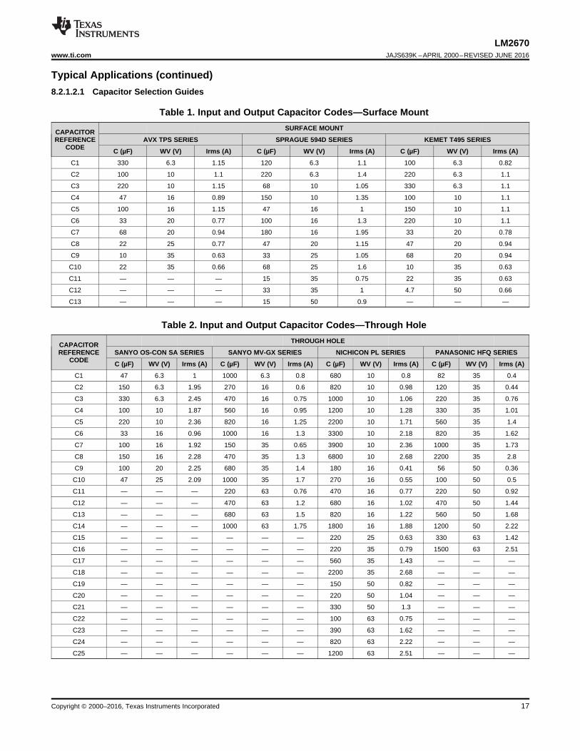
Step 5: Determine an input capacitor from Table 7 or Table 8 for fixed output voltage applications. Use Table 1or Table 2 to find the specific capacitor type. For adjustable output circuits select a capacitor from Table 1 orTable 2 with a sufficient working voltage (WV) rating greater than VIN max, and an RMS current rating greaterthan one-half the maximum load current (2 or more capacitors in parallel may be required).
Step 6: Select a diode from Table 4. The current rating of the diode must be greater than ILOAD max and thereverse voltage rating must be greater than VIN max.
Step 7: Include a 0.01-µF, 50-V capacitor for CBOOST in the design.
17
LM2670www.ti.com JAJS639K –APRIL 2000–REVISED JUNE 2016
Copyright © 2000–2016, Texas Instruments Incorporated
Typical Applications (continued)8.2.1.2.1 Capacitor Selection Guides
Table 1. Input and Output Capacitor Codes—Surface Mount
CAPACITORREFERENCE
CODE
SURFACE MOUNT
AVX TPS SERIES SPRAGUE 594D SERIES KEMET T495 SERIES
C (µF) WV (V) Irms (A) C (µF) WV (V) Irms (A) C (µF) WV (V) Irms (A)
C1 330 6.3 1.15 120 6.3 1.1 100 6.3 0.82
C2 100 10 1.1 220 6.3 1.4 220 6.3 1.1
C3 220 10 1.15 68 10 1.05 330 6.3 1.1
C4 47 16 0.89 150 10 1.35 100 10 1.1
C5 100 16 1.15 47 16 1 150 10 1.1
C6 33 20 0.77 100 16 1.3 220 10 1.1
C7 68 20 0.94 180 16 1.95 33 20 0.78
C8 22 25 0.77 47 20 1.15 47 20 0.94
C9 10 35 0.63 33 25 1.05 68 20 0.94
C10 22 35 0.66 68 25 1.6 10 35 0.63
C11 — — — 15 35 0.75 22 35 0.63
C12 — — — 33 35 1 4.7 50 0.66
C13 — — — 15 50 0.9 — — —
Table 2. Input and Output Capacitor Codes—Through Hole
CAPACITORREFERENCE
CODE
THROUGH HOLE
SANYO OS-CON SA SERIES SANYO MV-GX SERIES NICHICON PL SERIES PANASONIC HFQ SERIES
C (µF) WV (V) Irms (A) C (µF) WV (V) Irms (A) C (µF) WV (V) Irms (A) C (µF) WV (V) Irms (A)
C1 47 6.3 1 1000 6.3 0.8 680 10 0.8 82 35 0.4
C2 150 6.3 1.95 270 16 0.6 820 10 0.98 120 35 0.44
C3 330 6.3 2.45 470 16 0.75 1000 10 1.06 220 35 0.76
C4 100 10 1.87 560 16 0.95 1200 10 1.28 330 35 1.01
C5 220 10 2.36 820 16 1.25 2200 10 1.71 560 35 1.4
C6 33 16 0.96 1000 16 1.3 3300 10 2.18 820 35 1.62
C7 100 16 1.92 150 35 0.65 3900 10 2.36 1000 35 1.73
C8 150 16 2.28 470 35 1.3 6800 10 2.68 2200 35 2.8
C9 100 20 2.25 680 35 1.4 180 16 0.41 56 50 0.36
C10 47 25 2.09 1000 35 1.7 270 16 0.55 100 50 0.5
C11 — — — 220 63 0.76 470 16 0.77 220 50 0.92
C12 — — — 470 63 1.2 680 16 1.02 470 50 1.44
C13 — — — 680 63 1.5 820 16 1.22 560 50 1.68
C14 — — — 1000 63 1.75 1800 16 1.88 1200 50 2.22
C15 — — — — — — 220 25 0.63 330 63 1.42
C16 — — — — — — 220 35 0.79 1500 63 2.51
C17 — — — — — — 560 35 1.43 — — —
C18 — — — — — — 2200 35 2.68 — — —
C19 — — — — — — 150 50 0.82 — — —
C20 — — — — — — 220 50 1.04 — — —
C21 — — — — — — 330 50 1.3 — — —
C22 — — — — — — 100 63 0.75 — — —
C23 — — — — — — 390 63 1.62 — — —
C24 — — — — — — 820 63 2.22 — — —
C25 — — — — — — 1200 63 2.51 — — —
18
LM2670JAJS639K –APRIL 2000–REVISED JUNE 2016 www.ti.com
Copyright © 2000–2016, Texas Instruments Incorporated
8.2.1.2.2 Inductor Selection Guides
For Continuous Mode Operation
Table 3. Inductor Manufacturer Part NumbersINDUCTORREFERENC
ENUMBER
INDUCTANCE(µH)
CURRENT(A)
RENCO PULSE ENGINEERING COILCRAFT
THROUGH HOLE SURFACEMOUNT
THROUGHHOLE
SURFACEMOUNT SURFACE MOUNT
L23 33 1.35 RL-5471-7 RL1500-33 PE-53823 PE-53823S DO3316-333L24 22 1.65 RL-1283-22-43 RL1500-22 PE-53824 PE-53824S DO3316-223L25 15 2 RL-1283-15-43 RL1500-15 PE-53825 PE-53825S DO3316-153L29 100 1.41 RL-5471-4 RL-6050-100 PE-53829 PE-53829S DO5022P-104L30 68 1.71 RL-5471-5 RL6050-68 PE-53830 PE-53830S DO5022P-683L31 47 2.06 RL-5471-6 RL6050-47 PE-53831 PE-53831S DO5022P-473L32 33 2.46 RL-5471-7 RL6050-33 PE-53932 PE-53932S DO5022P-333L33 22 3.02 RL-1283-22-43 RL6050-22 PE-53933 PE-53933S DO5022P-223L34 15 3.65 RL-1283-15-43 — PE-53934 PE-53934S DO5022P-153L38 68 2.97 RL-5472-2 — PE-54038 PE-54038S —L39 47 3.57 RL-5472-3 — PE-54039 PE-54039S —L40 33 4.26 RL-1283-33-43 — PE-54040 PE-54040S —L41 22 5.22 RL-1283-22-43 — PE-54041 P0841 —L44 68 3.45 RL-5473-3 — PE-54044 — —L45 10 4.47 RL-1283-10-43 — — P0845 DO5022P-103HC
Table 4. Schottky Diode Selection TableREVERSEVOLTAGE
(V)
SURFACE MOUNT THROUGH HOLE
3 A 5 A OR MORE 3 A 5 A OR MORE
20 SK32 —1N5820
—SR302
30SK33
MBRD835L1N5821
—30WQ03F 31DQ03
40
SK34 MBRB1545CT 1N5822 —30BQ040
6TQ045S
MBR340 MBR74530WQ04F 31DQ04 80SQ045MBRS340
SR403 6TQ045MBRD340
50 or moreSK35
—MBR350
—30WQ05F
31DQ05SR305
19
LM2670www.ti.com JAJS639K –APRIL 2000–REVISED JUNE 2016
Copyright © 2000–2016, Texas Instruments Incorporated
8.2.1.3 Application Curves
Figure 17. LM2670 – 3.3 V Figure 18. LM2670 – 5 V
Figure 19. LM2670 – 12 V Figure 20. LM2670 – Adjustable
8.2.2 Fixed Output Voltage Application
Figure 21. Basic Circuit for Fixed Output Voltage Applications
20
LM2670JAJS639K –APRIL 2000–REVISED JUNE 2016 www.ti.com
Copyright © 2000–2016, Texas Instruments Incorporated
(1) No. represents the number of identical capacitor types to be connected in parallel(2) C Code indicates the Capacitor Reference number in Table 1 or Table 2 for identifying the specific component from the manufacturer
8.2.2.1 Design RequirementsSelect the power supply operating conditions and the maximum output current and follow below procedures tofind the external components for LM2670
8.2.2.2 Detailed Design ProcedureA system logic power supply bus of 3.3 V is to be generated from a wall adapter which provides an unregulatedDC voltage of 13 V to 16 V. The maximum load current is 2.5 A. Through-hole components are preferred.
Step 1: Operating conditions are:• VOUT = 3.3 V• VIN max = 16 V• ILOAD max = 2.5 A
Step 2: Select an LM2670T-3.3. The output voltage will have a tolerance of ±2% at room temperature and ±3%over the full operating temperature range.
Step 3: Use the nomograph for the 3.3-V device, Figure 17. The intersection of the 16 V horizontal line (VIN max)and the 2.5 A vertical line (ILOAD max) indicates that L33, a 22-µH inductor, is required.
From Table 3, L33 in a through-hole component is available from Renco with part number RL-1283-22-43 or partnumber PE-53933 from Pulse Engineering.
Step 4: Use Table 5 or Table 6 to determine an output capacitor. With a 3.3-V output and a 22-µH inductor thereare four through-hole output capacitor solutions with the number of same type capacitors to be paralleled and anidentifying capacitor code given. Table 1 or Table 2 provide the actual capacitor characteristics. Any of thefollowing choices will work in the circuit:• 1 × 220-µF, 10-V Sanyo OS-CON (code C5)• 1 × 1000-µF, 35-V Sanyo MV-GX (code C10)• 1 × 2200-µF, 10-V Nichicon PL (code C5)• 1 × 1000-µF, 35-V Panasonic HFQ (code C7)
Step 5: Use Table 7 or Table 8 to select an input capacitor. With 3.3-V output and 22 µH there are threethrough-hole solutions. These capacitors provide a sufficient voltage rating and an rms current rating greater than1.25 A (1/2 ILOAD max). Again using Table 1 or Table 2 for specific component characteristics the followingchoices are suitable:• 1 × 1000-µF, 63-V Sanyo MV-GX (code C14)• 1 × 820-µF, 63-V Nichicon PL (code C24)• 1 × 560-µF, 50-V Panasonic HFQ (code C13)
Step 6: From Table 4 a 3-A Schottky diode must be selected. For through-hole components 20-V rated diodesare sufficient. and 2 part types are suitable:• 1N5820• SR302
Step 7: A 0.01-µF capacitor is used for CBOOST.
8.2.2.2.1 Capacitor Selection Guides
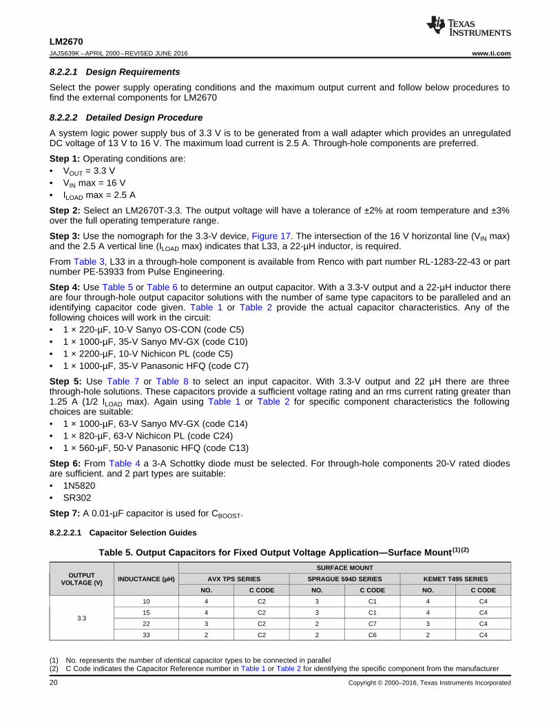
Table 5. Output Capacitors for Fixed Output Voltage Application—Surface Mount (1) (2)
OUTPUTVOLTAGE (V) INDUCTANCE (µH)
SURFACE MOUNT
AVX TPS SERIES SPRAGUE 594D SERIES KEMET T495 SERIES
NO. C CODE NO. C CODE NO. C CODE
3.3
10 4 C2 3 C1 4 C4
15 4 C2 3 C1 4 C4
22 3 C2 2 C7 3 C4
33 2 C2 2 C6 2 C4
21
LM2670www.ti.com JAJS639K –APRIL 2000–REVISED JUNE 2016
Copyright © 2000–2016, Texas Instruments Incorporated
Table 5. Output Capacitors for Fixed Output Voltage Application—Surface Mount()() (continued)
OUTPUTVOLTAGE (V) INDUCTANCE (µH)
SURFACE MOUNT
AVX TPS SERIES SPRAGUE 594D SERIES KEMET T495 SERIES
NO. C CODE NO. C CODE NO. C CODE
5
10 4 C2 4 C6 4 C4
15 3 C2 2 C7 3 C4
22 3 C2 2 C7 3 C4
33 2 C2 2 C3 2 C4
47 2 C2 1 C7 2 C4
12
10 4 C5 3 C6 5 C9
15 3 C5 2 C7 4 C8
22 2 C5 2 C6 3 C8
33 2 C5 1 C7 2 C8
47 2 C4 1 C6 2 C8
68 1 C5 1 C5 2 C7
100 1 C4 1 C5 1 C8
(1) No. represents the number of identical capacitor types to be connected in parallel(2) C Code indicates the Capacitor Reference number in Table 1 or Table 2 for identifying the specific component from the manufacturer
Table 6. Output Capacitors for Fixed Output Voltage Application—Through Hole (1) (2)
OUTPUTVOLTAGE (V)
INDUCTANCE(µH)
THROUGH HOLE
SANYO OS-CON SASERIES SANYO MV-GX SERIES NICHICON PL SERIES PANASONIC HFQ SERIES
NO. C CODE NO. C CODE NO. C CODE NO. C CODE
3.3
10 1 C3 1 C10 1 C6 2 C6
15 1 C3 1 C10 1 C6 2 C5
22 1 C5 1 C10 1 C5 1 C7
33 1 C2 1 C10 1 C13 1 C5
5
10 2 C4 1 C10 1 C6 2 C5
15 1 C5 1 C10 1 C5 1 C6
22 1 C5 1 C5 1 C5 1 C5
33 1 C4 1 C5 1 C13 1 C5
47 1 C4 1 C4 1 C13 2 C3
12
10 2 C7 1 C5 1 C18 2 C5
15 1 C8 1 C5 1 C17 1 C5
22 1 C7 1 C5 1 C13 1 C5
33 1 C7 1 C3 1 C11 1 C4
47 1 C7 1 C3 1 C10 1 C3
68 1 C7 1 C2 1 C10 1 C3
100 1 C7 1 C2 1 C9 1 C1
(1) Assumes worst case maximum input voltage and load current for a given inductance value(2) No. represents the number of identical capacitor types to be connected in parallel(3) C Code indicates the Capacitor Reference number in Table 1 or Table 2 for identifying the specific component from the manufacturer(4) Check voltage rating of capacitors to be greater than application input voltage
Table 7. Input Capacitors for Fixed Output Voltage Application—Surface Mount (1) (2) (3)
OUTPUTVOLTAGE (V) INDUCTANCE (µH)
SURFACE MOUNT
AVX TPS SERIES SPRAGUE 594D SERIES KEMET T495 SERIES
NO. C CODE NO. C CODE NO. C CODE
3.3
10 2 C5 1 C7 2 C8
15 3 C9 1 C10 3 C10
22 See (4) See (4) 2 C13 3 C12
33 See (4) See (4) 2 C13 2 C12
22
LM2670JAJS639K –APRIL 2000–REVISED JUNE 2016 www.ti.com
Copyright © 2000–2016, Texas Instruments Incorporated
Table 7. Input Capacitors for Fixed Output Voltage Application—Surface Mount()()() (continued)
OUTPUTVOLTAGE (V) INDUCTANCE (µH)
SURFACE MOUNT
AVX TPS SERIES SPRAGUE 594D SERIES KEMET T495 SERIES
NO. C CODE NO. C CODE NO. C CODE
5
10 2 C5 1 C7 2 C8
15 2 C5 1 C7 2 C8
22 3 C10 2 C12 3 C11
33 See (4) See (4) 2 C13 3 C12
47 See (4) See (4) 1 C13 2 C12
12
10 2 C7 2 C10 2 C7
15 2 C7 2 C10 2 C7
22 3 C10 2 C12 3 C10
33 3 C10 2 C12 3 C10
47 See (4) See (4) 2 C13 3 C12
68 See (4) See (4) 2 C13 2 C12
100 See (4) See (4) 1 C13 2 C12
(1) Assumes worst case maximum input voltage and load current for a given inductance value(2) No. represents the number of identical capacitor types to be connected in parallel(3) C Code indicates the Capacitor Reference number in Table 1 or Table 2 for identifying the specific component from the manufacturer(4) Check voltage rating of capacitors to be greater than application input voltage
Table 8. Input Capacitors for Fixed Output Voltage Application—Through Hole (1) (2) (3)
OUTPUTVOLTAGE (V)
INDUCTANCE(µH)
THROUGH HOLE
SANYO OS-CON SASERIES SANYO MV-GX SERIES NICHICON PL SERIES PANASONIC HFQ SERIES
NO. C CODE NO. C CODE NO. C CODE NO. C CODE
3.3
10 1 C7 2 C4 1 C5 1 C6
15 1 C10 1 C10 1 C18 1 C6
22 See (4) See (4) 1 C14 1 C24 1 C13
33 See (4) See (4) 1 C12 1 C20 1 C12
5
10 1 C7 2 C4 1 C14 1 C6
15 1 C7 2 C4 1 C14 1 C6
22 See (4) See (4) 1 C10 1 C18 1 C13
33 See (4) See (4) 1 C14 1 C23 1 C13
47 See (4) See (4) 1 C12 1 C20 1 C12
12
10 1 C9 1 C10 1 C18 1 C6
15 1 C10 1 C10 1 C18 1 C6
22 1 C10 1 C10 1 C18 1 C6
33 See (4) See (4) 1 C10 1 C18 1 C6
47 See (4) See (4) 1 C13 1 C23 1 C13
68 See (4) See (4) 1 C12 1 C21 1 C12
100 See (4) See (4) 1 C11 1 C22 1 C11
23
LM2670www.ti.com JAJS639K –APRIL 2000–REVISED JUNE 2016
Copyright © 2000–2016, Texas Instruments Incorporated
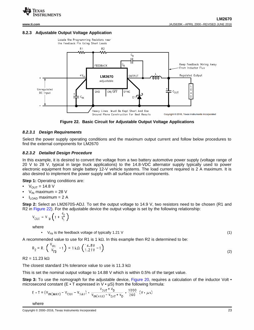
8.2.3 Adjustable Output Voltage Application
Figure 22. Basic Circuit for Adjustable Output Voltage Applications
8.2.3.1 Design RequirementsSelect the power supply operating conditions and the maximum output current and follow below procedures tofind the external components for LM2670
8.2.3.2 Detailed Design ProcedureIn this example, it is desired to convert the voltage from a two battery automotive power supply (voltage range of20 V to 28 V, typical in large truck applications) to the 14.8-VDC alternator supply typically used to powerelectronic equipment from single battery 12-V vehicle systems. The load current required is 2 A maximum. It isalso desired to implement the power supply with all surface mount components.
Step 1: Operating conditions are:• VOUT = 14.8 V• VIN maximum = 28 V• ILOAD maximum = 2 A
Step 2: Select an LM2670S-ADJ. To set the output voltage to 14.9 V, two resistors need to be chosen (R1 andR2 in Figure 22). For the adjustable device the output voltage is set by the following relationship:
where• VFB is the feedback voltage of typically 1.21 V (1)
A recommended value to use for R1 is 1 kΩ. In this example then R2 is determined to be:
(2)
R2 = 11.23 kΩ
The closest standard 1% tolerance value to use is 11.3 kΩ
This is set the nominal output voltage to 14.88 V which is within 0.5% of the target value.
Step 3: To use the nomograph for the adjustable device, Figure 20, requires a calculation of the inductor Volt •microsecond constant (E • T expressed in V • µS) from the following formula:
where
24
LM2670JAJS639K –APRIL 2000–REVISED JUNE 2016 www.ti.com
Copyright © 2000–2016, Texas Instruments Incorporated
• VSAT is the voltage drop across the internal power switch which is Rds(ON) times ILOAD (3)
In this example this would be typically 0.15 Ω × 2 A or 0.3 V and VD is the voltage drop across the forwardbiased Schottky diode, typically 0.5 V. The switching frequency of 260 kHz is the nominal value to use toestimate the ON time of the switch during which energy is stored in the inductor.
For this example E • T is found to be:
(4)
(5)
Using Figure 20, the intersection of 27 V • µS horizontally and the 2 A vertical line (ILOAD max) indicates that L38,a 68-µH inductor, must be used.
From Table 3, L38 in a surface mount component is available from Pulse Engineering with part number PE-54038S.
Step 4: Use Table 9 or Table 10 to determine an output capacitor. With a 14.8-V output the 12.5 to 15 V row isused and with a 68-µH inductor there are three surface mount output capacitor solutions. Table 1 or Table 2provides the actual capacitor characteristics based on the C Code number. Any of the following choices can beused:• 1 × 33-µF, 20-V AVX TPS (code C6)• 1 × 47-µF, 20-V Sprague 594 (code C8)• 1 × 47-µF, 20-V Kemet T495 (code C8)
NOTEWhen using the adjustable device in low voltage applications (less than 3-V output), if thenomograph, Figure 20, selects an inductance of 22 µH or less, Table 9 and Table 10 donot provide an output capacitor solution. With these conditions the number of outputcapacitors required for stable operation becomes impractical. TI recommends using eithera 33-µH or 47-µH inductor and the output capacitors from Table 9 or Table 10.
Step 5: An input capacitor for this example will require at least a 35-V WV rating with an RMS current rating of 1A (1/2 IOUT max). From Table 1 or Table 2 it can be seen that C12, a 33-µF, 35-V capacitor from Sprague, hasthe required voltage and current rating of the surface mount components.
Step 6: From Table 4 a 3-A Schottky diode must be selected. For surface mount diodes with a margin of safetyon the voltage rating one of five diodes can be used:• SK34• 30BQ040• 30WQ04F• MBRS340• MBRD340
Step 7: A 0.01-µF capacitor is used for CBOOST.
25
LM2670www.ti.com JAJS639K –APRIL 2000–REVISED JUNE 2016
Copyright © 2000–2016, Texas Instruments Incorporated
(1) No. represents the number of identical capacitor types to be connected in parallel(2) C Code indicates the Capacitor Reference number in Table 1 or Table 2 for identifying the specific component from the manufacturer(3) Set to a higher value for a practical design solution.
8.2.3.2.1 Capacitor Selection Guides
Table 9. Output Capacitors for Adjustable Output Voltage Applications—Surface Mount (1) (2)
OUTPUT VOLTAGE (V) INDUCTANCE(µH)
SURFACE MOUNT
AVX TPS SERIES SPRAGUE 594D SERIES KEMET T495 SERIES
NO. C CODE NO. C CODE NO. C CODE
1.21 to 2.533 (3) 7 C1 6 C2 7 C3
47 (3) 5 C1 4 C2 5 C3
2.5 to 3.7533 (3) 4 C1 3 C2 4 C3
47 (3) 3 C1 2 C2 3 C3
3.75 to 5
22 4 C1 3 C2 4 C3
33 3 C1 2 C2 3 C3
47 2 C1 2 C2 2 C3
5 to 6.25
22 3 C2 1 C3 3 C4
33 2 C2 2 C3 2 C4
47 2 C2 2 C3 2 C4
68 1 C2 1 C3 1 C4
6.25 to 7.5
22 3 C2 1 C4 3 C4
33 2 C2 1 C3 2 C4
47 1 C3 1 C4 1 C6
68 1 C2 1 C3 1 C4
7.5 to 10
33 2 C5 1 C6 2 C8
47 1 C5 1 C6 2 C8
68 1 C5 1 C6 1 C8
100 1 C4 1 C5 1 C8
10 to 12.5
33 1 C5 1 C6 2 C8
47 1 C5 1 C6 2 C8
68 1 C5 1 C6 1 C8
100 1 C5 1 C6 1 C8
12.5 to 15
33 1 C6 1 C8 1 C8
47 1 C6 1 C8 1 C8
68 1 C6 1 C8 1 C8
100 1 C6 1 C8 1 C8
15 to 20
33 1 C8 1 C10 2 C10
47 1 C8 1 C9 2 C10
68 1 C8 1 C9 2 C10
100 1 C8 1 C9 1 C10
20 to 30
33 2 C9 2 C11 2 C11
47 1 C10 1 C12 1 C11
68 1 C9 1 C12 1 C11
100 1 C9 1 C12 1 C11
30 to 37
10
No Values Available
4 C13 8 C12
15 3 C13 5 C12
22 2 C13 4 C12
33 1 C13 3 C12
47 1 C13 2 C12
68 1 C13 2 C12
26
LM2670JAJS639K –APRIL 2000–REVISED JUNE 2016 www.ti.com
Copyright © 2000–2016, Texas Instruments Incorporated
(1) No. represents the number of identical capacitor types to be connected in parallel(2) C Code indicates the Capacitor Reference number in Table 1 or Table 2 for identifying the specific component from the manufacturer(3) Set to a higher value for a practical design solution.
Table 10. Output Capacitors for Adjustable Output Voltage Applications—Through Hole (1) (2)
OUTPUT VOLTAGE(V)
INDUCTANCE(µH)
THROUGH HOLE
SANYO OS-CON SASERIES SANYO MV-GX SERIES NICHICON PL SERIES PANASONIC HFQ
SERIES
NO. C CODE NO. C CODE NO. C CODE NO. C CODE
1.21 to 2.533 (3) 2 C3 5 C1 5 C3 3 C
47 (3) 2 C2 4 C1 3 C3 2 C5
2.5 to 3.7533 (3) 1 C3 3 C1 3 C1 2 C5
47 (3) 1 C2 2 C1 2 C3 1 C5
3.75 to 5
22 1 C3 3 C1 3 C1 2 C5
33 1 C2 2 C1 2 C1 1 C5
47 1 C2 2 C1 1 C3 1 C5
5 to 6.25
22 1 C5 2 C6 2 C3 2 C5
33 1 C4 1 C6 2 C1 1 C5
47 1 C4 1 C6 1 C3 1 C5
68 1 C4 1 C6 1 C1 1 C5
6.25 to 7.5
22 1 C5 1 C6 2 C1 1 C5
33 1 C4 1 C6 1 C3 1 C5
47 1 C4 1 C6 1 C1 1 C5
68 1 C4 1 C2 1 C1 1 C5
7.5 to 10
33 1 C7 1 C6 1 C14 1 C5
47 1 C7 1 C6 1 C14 1 C5
68 1 C7 1 C2 1 C14 1 C2
100 1 C7 1 C2 1 C14 1 C2
10 to 12.5
33 1 C7 1 C6 1 C14 1 C5
47 1 C7 1 C2 1 C14 1 C5
68 1 C7 1 C2 1 C9 1 C2
100 1 C7 1 C2 1 C9 1 C2
12.5 to 15
33 1 C9 1 C10 1 C15 1 C2
47 1 C9 1 C10 1 C15 1 C2
68 1 C9 1 C10 1 C15 1 C2
100 1 C9 1 C10 1 C15 1 C2
15 to 20
33 1 C10 1 C7 1 C15 1 C2
47 1 C10 1 C7 1 C15 1 C2
68 1 C10 1 C7 1 C15 1 C2
100 1 C10 1 C7 1 C15 1 C2
20 to 30
33
No Values Available
1 C7 1 C16 1 C2
47 1 C7 1 C16 1 C2
68 1 C7 1 C16 1 C2
100 1 C7 1 C16 1 C2
30 to 37
10
No Values Available
1 C12 1 C20 1 C10
15 1 C11 1 C20 1 C11
22 1 C11 1 C20 1 C10
33 1 C11 1 C20 1 C10
47 1 C11 1 C20 1 C10
68 1 C11 1 C20 1 C10
9 Power Supply RecommendationsThe LM2670 is designed to operate from an input voltage supply up to 40 V. This input supply must be wellregulated and able to withstand maximum input current and maintain a stable voltage.
27
LM2670www.tij.co.jp JAJS639K –APRIL 2000–REVISED JUNE 2016
Copyright © 2000–2016, Texas Instruments Incorporated
10 Layout
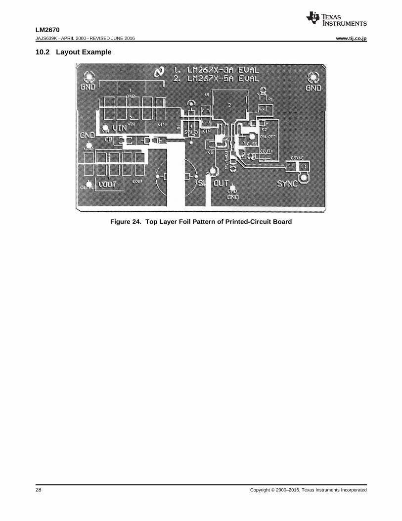
10.1 Layout GuidelinesBoard layout is critical for the proper operation of switching power supplies. First, the ground plane area must besufficient for thermal dissipation purposes. Second, appropriate guidelines must be followed to reduce the effectsof switching noise. Switch mode converters are very fast switching devices. In such cases, the rapid increase ofinput current combined with the parasitic trace inductance generates unwanted L di/dt noise spikes. Themagnitude of this noise tends to increase as the output current increases. This noise may turn intoelectromagnetic interference (EMI) and can also cause problems in device performance. Therefore, take care inlayout to minimize the effect of this switching noise. The most important layout rule is to keep the AC currentloops as small as possible. Figure 23 shows the current flow in a buck converter. The top schematic shows adotted line which represents the current flow during the top switch ON-state. The middle schematic shows thecurrent flow during the top switch OFF-state. The bottom schematic shows the currents referred to as accurrents. These AC currents are the most critical because they are changing in a very short time period. Thedotted lines of the bottom schematic are the traces to keep as short and wide as possible. This also yields asmall loop area reducing the loop inductance. To avoid functional problems due to layout, review the PCB layoutexample. Best results are achieved if the placement of the LM2679 device, the bypass capacitor, the Schottkydiode, RFBB, RFBT, and the inductor are placed as shown in the example. Note that, in the layout shown, R1 =RFBB and R2 = RFBT. TI also recommends using 2-oz. copper boards or heavier to help thermal dissipation andto reduce the parasitic inductances of board traces. See application note AN-1229 SIMPLE SWITCHER® PCBLayout Guidelines for more information.
Figure 23. Typical Current Flow on a Buck Converter
28
LM2670JAJS639K –APRIL 2000–REVISED JUNE 2016 www.tij.co.jp
Copyright © 2000–2016, Texas Instruments Incorporated
10.2 Layout Example
Figure 24. Top Layer Foil Pattern of Printed-Circuit Board
29
LM2670www.tij.co.jp JAJS639K –APRIL 2000–REVISED JUNE 2016
Copyright © 2000–2016, Texas Instruments Incorporated
11 デデババイイススおおよよびびドドキキュュメメンントトののササポポーートト
11.1 デデババイイスス・・ササポポーートト
11.1.1 デデベベロロッッパパーー・・ネネッットトワワーーククのの製製品品にに関関すするる免免責責事事項項デベロッパー・ネットワークの製品またはサービスに関するTIの出版物は、単独またはTIの製品、サービスと一緒に提供される場合に関係なく、デベロッパー・ネットワークの製品またはサービスの適合性に関する是認、デベロッパー・ネットワークの製品またはサービスの是認の表明を意味するものではありません。
11.2 関関連連資資料料関連資料については、以下を参照してください。
• 『AN-1187 リードレス・リードフレーム・パッケージ(LLP)』• 『AN-1229 SIMPLE SWITCHER® PCBレイアウト・ガイドライン』
11.3 ドドキキュュメメンントトのの更更新新通通知知をを受受けけ取取るる方方法法ドキュメントの更新についての通知を受け取るには、ti.comのデバイス製品フォルダを開いてください。右上の隅にある「通知を受け取る」をクリックして登録すると、変更されたすべての製品情報に関するダイジェストを毎週受け取れます。変更の詳細については、修正されたドキュメントに含まれている改訂履歴をご覧ください。
11.4 ココミミュュニニテティィ・・リリソソーーススThe following links connect to TI community resources. Linked contents are provided "AS IS" by the respectivecontributors. They do not constitute TI specifications and do not necessarily reflect TI's views; see TI's Terms ofUse.
TI E2E™ Online Community TI's Engineer-to-Engineer (E2E) Community. Created to foster collaborationamong engineers. At e2e.ti.com, you can ask questions, share knowledge, explore ideas and helpsolve problems with fellow engineers.
Design Support TI's Design Support Quickly find helpful E2E forums along with design support tools andcontact information for technical support.
11.5 商商標標E2E is a trademark of Texas Instruments.SIMPLE SWITCHER is a registered trademark of Texas Instruments.All other trademarks are the property of their respective owners.
11.6 静静電電気気放放電電にに関関すするる注注意意事事項項これらのデバイスは、限定的なESD(静電破壊)保護機能を内 蔵しています。保存時または取り扱い時は、MOSゲートに対す る静電破壊を防止するために、リード線同士をショートさせて おくか、デバイスを導電フォームに入れる必要があります。
11.7 GlossarySLYZ022 — TI Glossary.
This glossary lists and explains terms, acronyms, and definitions.
12 メメカカニニカカルル、、パパッッケケーージジ、、おおよよびび注注文文情情報報以降のページには、メカニカル、パッケージ、および注文に関する情報が記載されています。これらの情報は、指定のデバイスに対して提供されている最新のデータです。このデータは予告なく変更されることがあり、ドキュメントが改訂される場合もあります。本データシートのブラウザ版を使用されている場合は、画面左側の説明をご覧ください。
12.1 DAP (VSONパパッッケケーージジ)プリント基板のグラウンド・プレーンまたはアイランドには、ダイ取り付けパッド(DAP)を接続でき、接続する必要があります。CADおよび組み立てのガイドラインについては、アプリケーション・ノートAN-1187(www.ti.com/lsds/ti/analog/powermanagement/power_portal.page)を参照してください。
PACKAGE OPTION ADDENDUM
www.ti.com 30-Sep-2021
Addendum-Page 1
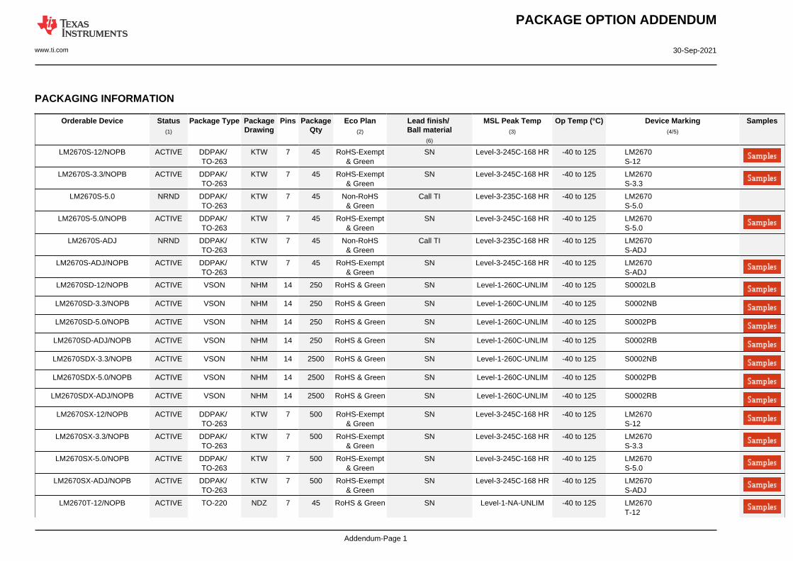
PACKAGING INFORMATION
Orderable Device Status(1)
Package Type PackageDrawing
Pins PackageQty
Eco Plan(2)
Lead finish/Ball material
(6)
MSL Peak Temp(3)
Op Temp (°C) Device Marking(4/5)
Samples
LM2670S-12/NOPB ACTIVE DDPAK/TO-263
KTW 7 45 RoHS-Exempt& Green
SN Level-3-245C-168 HR -40 to 125 LM2670S-12
LM2670S-3.3/NOPB ACTIVE DDPAK/TO-263
KTW 7 45 RoHS-Exempt& Green
SN Level-3-245C-168 HR -40 to 125 LM2670S-3.3
LM2670S-5.0 NRND DDPAK/TO-263
KTW 7 45 Non-RoHS& Green
Call TI Level-3-235C-168 HR -40 to 125 LM2670S-5.0
LM2670S-5.0/NOPB ACTIVE DDPAK/TO-263
KTW 7 45 RoHS-Exempt& Green
SN Level-3-245C-168 HR -40 to 125 LM2670S-5.0
LM2670S-ADJ NRND DDPAK/TO-263
KTW 7 45 Non-RoHS& Green
Call TI Level-3-235C-168 HR -40 to 125 LM2670S-ADJ
LM2670S-ADJ/NOPB ACTIVE DDPAK/TO-263
KTW 7 45 RoHS-Exempt& Green
SN Level-3-245C-168 HR -40 to 125 LM2670S-ADJ
LM2670SD-12/NOPB ACTIVE VSON NHM 14 250 RoHS & Green SN Level-1-260C-UNLIM -40 to 125 S0002LB
LM2670SD-3.3/NOPB ACTIVE VSON NHM 14 250 RoHS & Green SN Level-1-260C-UNLIM -40 to 125 S0002NB
LM2670SD-5.0/NOPB ACTIVE VSON NHM 14 250 RoHS & Green SN Level-1-260C-UNLIM -40 to 125 S0002PB
LM2670SD-ADJ/NOPB ACTIVE VSON NHM 14 250 RoHS & Green SN Level-1-260C-UNLIM -40 to 125 S0002RB
LM2670SDX-3.3/NOPB ACTIVE VSON NHM 14 2500 RoHS & Green SN Level-1-260C-UNLIM -40 to 125 S0002NB
LM2670SDX-5.0/NOPB ACTIVE VSON NHM 14 2500 RoHS & Green SN Level-1-260C-UNLIM -40 to 125 S0002PB
LM2670SDX-ADJ/NOPB ACTIVE VSON NHM 14 2500 RoHS & Green SN Level-1-260C-UNLIM -40 to 125 S0002RB
LM2670SX-12/NOPB ACTIVE DDPAK/TO-263
KTW 7 500 RoHS-Exempt& Green
SN Level-3-245C-168 HR -40 to 125 LM2670S-12
LM2670SX-3.3/NOPB ACTIVE DDPAK/TO-263
KTW 7 500 RoHS-Exempt& Green
SN Level-3-245C-168 HR -40 to 125 LM2670S-3.3
LM2670SX-5.0/NOPB ACTIVE DDPAK/TO-263
KTW 7 500 RoHS-Exempt& Green
SN Level-3-245C-168 HR -40 to 125 LM2670S-5.0
LM2670SX-ADJ/NOPB ACTIVE DDPAK/TO-263
KTW 7 500 RoHS-Exempt& Green
SN Level-3-245C-168 HR -40 to 125 LM2670S-ADJ
LM2670T-12/NOPB ACTIVE TO-220 NDZ 7 45 RoHS & Green SN Level-1-NA-UNLIM -40 to 125 LM2670T-12
PACKAGE OPTION ADDENDUM
www.ti.com 30-Sep-2021
Addendum-Page 2
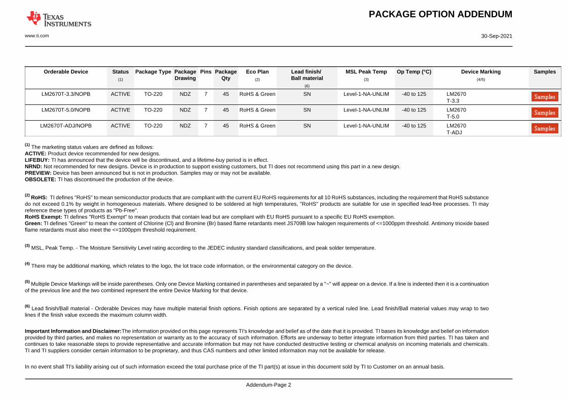
Orderable Device Status(1)
Package Type PackageDrawing
Pins PackageQty
Eco Plan(2)
Lead finish/Ball material
(6)
MSL Peak Temp(3)
Op Temp (°C) Device Marking(4/5)
Samples
LM2670T-3.3/NOPB ACTIVE TO-220 NDZ 7 45 RoHS & Green SN Level-1-NA-UNLIM -40 to 125 LM2670T-3.3
LM2670T-5.0/NOPB ACTIVE TO-220 NDZ 7 45 RoHS & Green SN Level-1-NA-UNLIM -40 to 125 LM2670T-5.0
LM2670T-ADJ/NOPB ACTIVE TO-220 NDZ 7 45 RoHS & Green SN Level-1-NA-UNLIM -40 to 125 LM2670T-ADJ
(1) The marketing status values are defined as follows:ACTIVE: Product device recommended for new designs.LIFEBUY: TI has announced that the device will be discontinued, and a lifetime-buy period is in effect.NRND: Not recommended for new designs. Device is in production to support existing customers, but TI does not recommend using this part in a new design.PREVIEW: Device has been announced but is not in production. Samples may or may not be available.OBSOLETE: TI has discontinued the production of the device.
(2) RoHS: TI defines "RoHS" to mean semiconductor products that are compliant with the current EU RoHS requirements for all 10 RoHS substances, including the requirement that RoHS substancedo not exceed 0.1% by weight in homogeneous materials. Where designed to be soldered at high temperatures, "RoHS" products are suitable for use in specified lead-free processes. TI mayreference these types of products as "Pb-Free".RoHS Exempt: TI defines "RoHS Exempt" to mean products that contain lead but are compliant with EU RoHS pursuant to a specific EU RoHS exemption.Green: TI defines "Green" to mean the content of Chlorine (Cl) and Bromine (Br) based flame retardants meet JS709B low halogen requirements of <=1000ppm threshold. Antimony trioxide basedflame retardants must also meet the <=1000ppm threshold requirement.
(3) MSL, Peak Temp. - The Moisture Sensitivity Level rating according to the JEDEC industry standard classifications, and peak solder temperature.
(4) There may be additional marking, which relates to the logo, the lot trace code information, or the environmental category on the device.
(5) Multiple Device Markings will be inside parentheses. Only one Device Marking contained in parentheses and separated by a "~" will appear on a device. If a line is indented then it is a continuationof the previous line and the two combined represent the entire Device Marking for that device.
(6) Lead finish/Ball material - Orderable Devices may have multiple material finish options. Finish options are separated by a vertical ruled line. Lead finish/Ball material values may wrap to twolines if the finish value exceeds the maximum column width.
Important Information and Disclaimer:The information provided on this page represents TI's knowledge and belief as of the date that it is provided. TI bases its knowledge and belief on informationprovided by third parties, and makes no representation or warranty as to the accuracy of such information. Efforts are underway to better integrate information from third parties. TI has taken andcontinues to take reasonable steps to provide representative and accurate information but may not have conducted destructive testing or chemical analysis on incoming materials and chemicals.TI and TI suppliers consider certain information to be proprietary, and thus CAS numbers and other limited information may not be available for release.
In no event shall TI's liability arising out of such information exceed the total purchase price of the TI part(s) at issue in this document sold by TI to Customer on an annual basis.
PACKAGE OPTION ADDENDUM
www.ti.com 30-Sep-2021
Addendum-Page 3
TAPE AND REEL INFORMATION
*All dimensions are nominal
Device PackageType
PackageDrawing
Pins SPQ ReelDiameter
(mm)
ReelWidth
W1 (mm)
A0(mm)
B0(mm)
K0(mm)
P1(mm)
W(mm)
Pin1Quadrant
LM2670SD-12/NOPB VSON NHM 14 250 178.0 16.4 5.3 6.3 1.5 12.0 16.0 Q1
LM2670SD-3.3/NOPB VSON NHM 14 250 178.0 16.4 5.3 6.3 1.5 12.0 16.0 Q1
LM2670SD-5.0/NOPB VSON NHM 14 250 178.0 16.4 5.3 6.3 1.5 12.0 16.0 Q1
LM2670SD-ADJ/NOPB VSON NHM 14 250 178.0 16.4 5.3 6.3 1.5 12.0 16.0 Q1
LM2670SDX-3.3/NOPB VSON NHM 14 2500 330.0 16.4 5.3 6.3 1.5 12.0 16.0 Q1
LM2670SDX-5.0/NOPB VSON NHM 14 2500 330.0 16.4 5.3 6.3 1.5 12.0 16.0 Q1
LM2670SDX-ADJ/NOPB VSON NHM 14 2500 330.0 16.4 5.3 6.3 1.5 12.0 16.0 Q1
LM2670SX-12/NOPB DDPAK/TO-263
KTW 7 500 330.0 24.4 10.75 14.85 5.0 16.0 24.0 Q2
LM2670SX-3.3/NOPB DDPAK/TO-263
KTW 7 500 330.0 24.4 10.75 14.85 5.0 16.0 24.0 Q2
LM2670SX-5.0/NOPB DDPAK/TO-263
KTW 7 500 330.0 24.4 10.75 14.85 5.0 16.0 24.0 Q2
LM2670SX-ADJ/NOPB DDPAK/TO-263
KTW 7 500 330.0 24.4 10.75 14.85 5.0 16.0 24.0 Q2
PACKAGE MATERIALS INFORMATION
www.ti.com 8-Mar-2019
Pack Materials-Page 1
*All dimensions are nominal
Device Package Type Package Drawing Pins SPQ Length (mm) Width (mm) Height (mm)
LM2670SD-12/NOPB VSON NHM 14 250 210.0 185.0 35.0
LM2670SD-3.3/NOPB VSON NHM 14 250 210.0 185.0 35.0
LM2670SD-5.0/NOPB VSON NHM 14 250 210.0 185.0 35.0
LM2670SD-ADJ/NOPB VSON NHM 14 250 210.0 185.0 35.0
LM2670SDX-3.3/NOPB VSON NHM 14 2500 367.0 367.0 35.0
LM2670SDX-5.0/NOPB VSON NHM 14 2500 367.0 367.0 35.0
LM2670SDX-ADJ/NOPB VSON NHM 14 2500 367.0 367.0 35.0
LM2670SX-12/NOPB DDPAK/TO-263 KTW 7 500 367.0 367.0 45.0
LM2670SX-3.3/NOPB DDPAK/TO-263 KTW 7 500 367.0 367.0 45.0
LM2670SX-5.0/NOPB DDPAK/TO-263 KTW 7 500 367.0 367.0 45.0
LM2670SX-ADJ/NOPB DDPAK/TO-263 KTW 7 500 367.0 367.0 45.0
PACKAGE MATERIALS INFORMATION
www.ti.com 8-Mar-2019
Pack Materials-Page 2
MECHANICAL DATA
NDZ0007B
www.ti.com
TA07B (Rev E)
MECHANICAL DATA
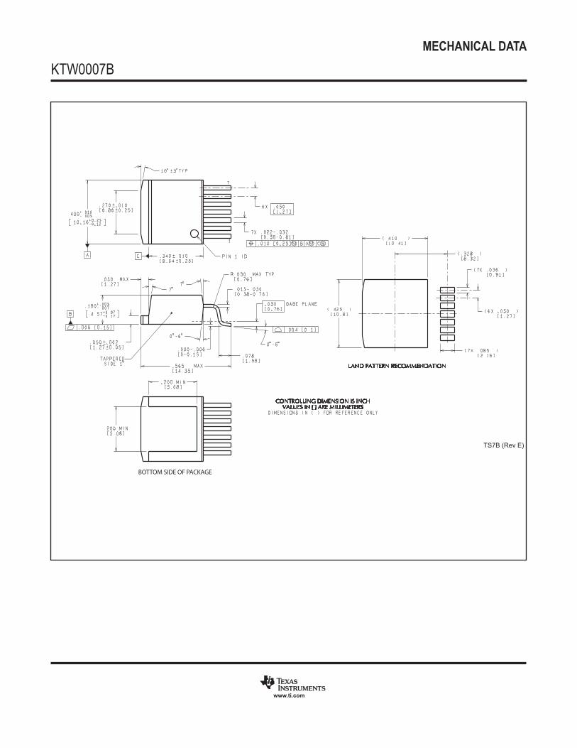
KTW0007B
www.ti.com
BOTTOM SIDE OF PACKAGE
TS7B (Rev E)
MECHANICAL DATA
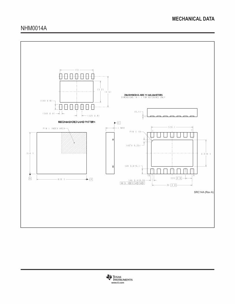
NHM0014A
www.ti.com
SRC14A (Rev A)
重要なお知らせと免責事項TI は、技術データと信頼性データ (データシートを含みます)、設計リソース (リファレンス・デザインを含みます)、アプリケーションや設計に関する各種アドバイス、Web ツール、安全性情報、その他のリソースを、欠陥が存在する可能性のある「現状のまま」提供しており、商品性および特定目的に対する適合性の黙示保証、第三者の知的財産権の非侵害保証を含むいかなる保証も、明示的または黙示的にかかわらず拒否します。これらのリソースは、TI 製品を使用する設計の経験を積んだ開発者への提供を意図したものです。(1) お客様のアプリケーションに適した TI 製品の選定、(2) お客様のアプリケーションの設計、検証、試験、(3) お客様のアプリケーションに該当する各種規格や、その他のあらゆる安全性、セキュリティ、規制、または他の要件への確実な適合に関する責任を、お客様のみが単独で負うものとします。上記の各種リソースは、予告なく変更される可能性があります。これらのリソースは、リソースで説明されている TI 製品を使用するアプリケーションの開発の目的でのみ、TI はその使用をお客様に許諾します。これらのリソースに関して、他の目的で複製することや掲載することは禁止されています。TI や第三者の知的財産権のライセンスが付与されている訳ではありません。お客様は、これらのリソースを自身で使用した結果発生するあらゆる申し立て、損害、費用、損失、責任について、TI およびその代理人を完全に補償するものとし、TI は一切の責任を拒否します。TI の製品は、TI の販売条件、または ti.com やかかる TI 製品の関連資料などのいずれかを通じて提供する適用可能な条項の下で提供されています。TI がこれらのリソースを提供することは、適用される TI の保証または他の保証の放棄の拡大や変更を意味するものではありません。お客様がいかなる追加条項または代替条項を提案した場合でも、TI はそれらに異議を唱え、拒否します。IMPORTANT NOTICE
郵送先住所:Texas Instruments, Post Office Box 655303, Dallas, Texas 75265Copyright © 2021, Texas Instruments Incorporated