Lecture 2 High-Speed I/O - Stanford University · –T =d L/ ν, bits arrive at a ... M Horowitz...
37
EE371 Lecture 2 M Horowitz 1 Lecture 2 High-Speed I/O Mark Horowitz Computer Systems Laboratory Stanford University [email protected] Copyright © 2007 by Mark Horowitz, with material from Stefanos Sidiropoulos, and Vladimir Stojanovic
Transcript of Lecture 2 High-Speed I/O - Stanford University · –T =d L/ ν, bits arrive at a ... M Horowitz...
EE371 Lecture 2M Horowitz 1
Lecture 2
High-Speed I/O
Mark HorowitzComputer Systems Laboratory
Stanford [email protected]
Copyright © 2007 by Mark Horowitz, with material from Stefanos Sidiropoulos, and Vladimir Stojanovic
EE371 Lecture 2M Horowitz 2
Readings
• Readings– Techniques for High-speed Implementation of Nonlinear
Cancellation, Sanjay Kasturia and Jack H. Winters
• Overview:– Your project will be the design of a circuit that processes the
input data from a high-speed I/O. This processing is generally done in a mixed signal manner today, but your job will be to build a digital implementation of the algorithm. This lecture will try to give you some background about why I/O rates are important, and what issues need to be resolved to achieve high performance. The next lecture will discuss the operation of the circuit you need to build.
EE371 Lecture 2M Horowitz 3
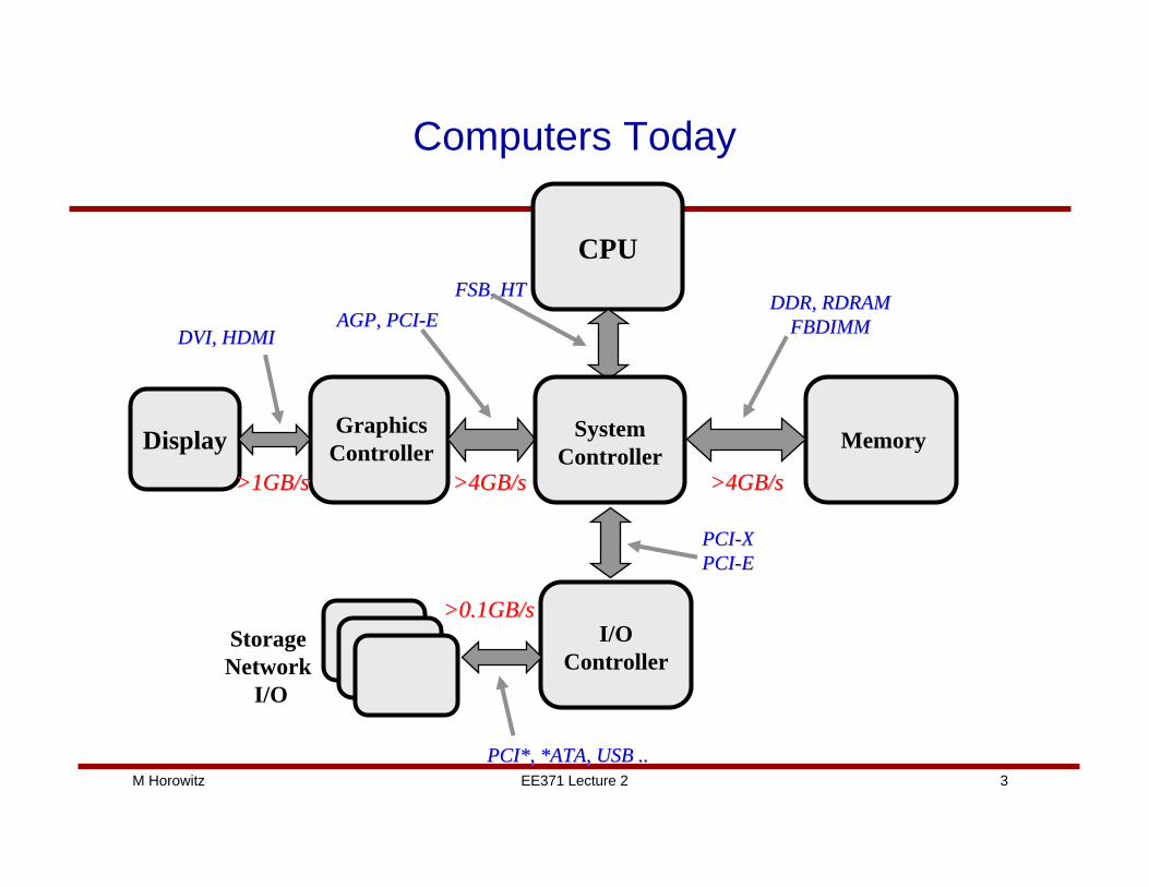
Computers Today
CPU
Memory
I/OController
GraphicsControllerDisplay
Storage Network
I/O
>1GB/s>1GB/s >4GB/s>4GB/s >4GB/s>4GB/s
>0.1GB/s>0.1GB/s
DDR, RDRAMDDR, RDRAMFBDIMMFBDIMM
FSB, HTFSB, HTAGP, PCIAGP, PCI--EE
PCIPCI--XXPCIPCI--EE
PCI*, *ATA, USB ..PCI*, *ATA, USB ..
DVI, HDMIDVI, HDMI
SystemController
EE371 Lecture 2M Horowitz 4
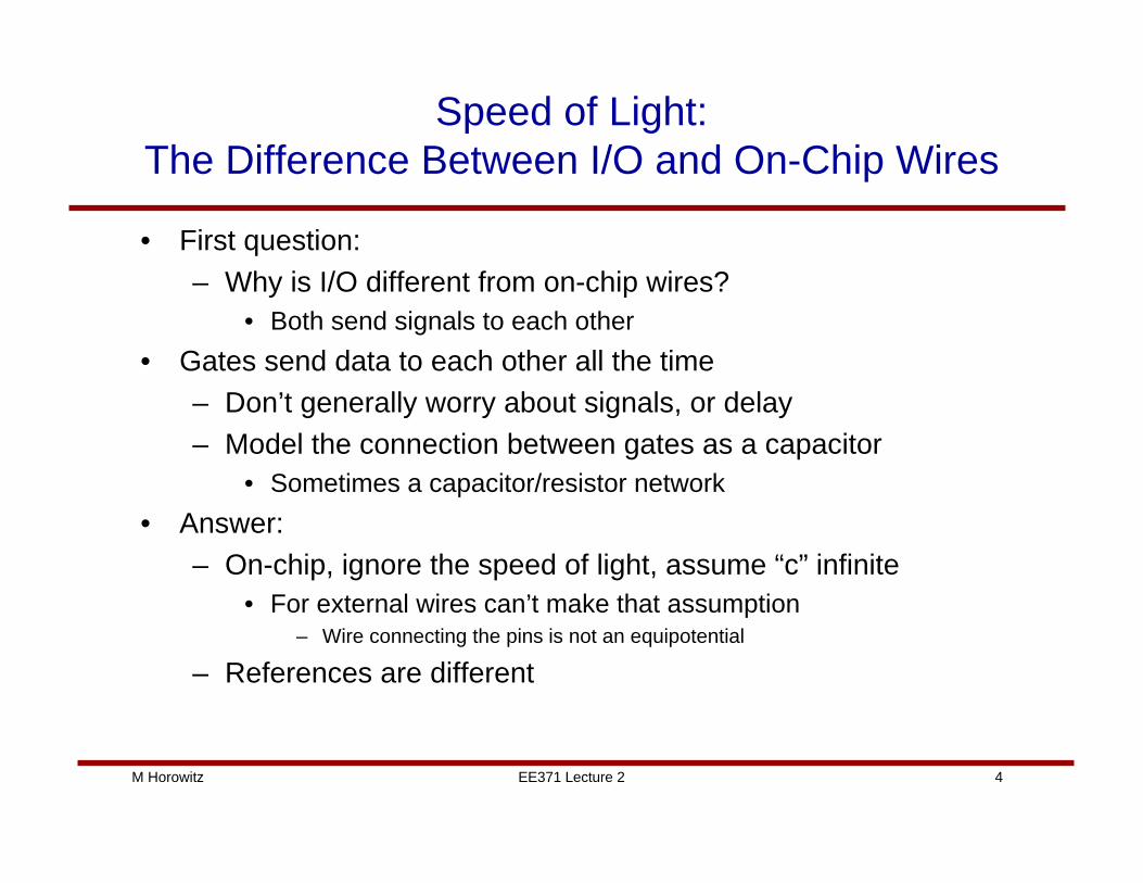
Speed of Light:The Difference Between I/O and On-Chip Wires
• First question:– Why is I/O different from on-chip wires?
• Both send signals to each other• Gates send data to each other all the time
– Don’t generally worry about signals, or delay– Model the connection between gates as a capacitor
• Sometimes a capacitor/resistor network• Answer:
– On-chip, ignore the speed of light, assume “c” infinite• For external wires can’t make that assumption
– Wire connecting the pins is not an equipotential
– References are different
EE371 Lecture 2M Horowitz 5
Finite Speed of Light Ramifications
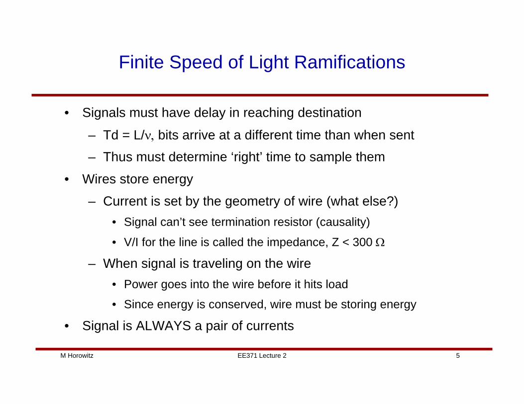
• Signals must have delay in reaching destination
– Td = L/ν, bits arrive at a different time than when sent– Thus must determine ‘right’ time to sample them
• Wires store energy
– Current is set by the geometry of wire (what else?)• Signal can’t see termination resistor (causality)
• V/I for the line is called the impedance, Z < 300 Ω
– When signal is traveling on the wire• Power goes into the wire before it hits load
• Since energy is conserved, wire must be storing energy
• Signal is ALWAYS a pair of currents
EE371 Lecture 2M Horowitz 6
Link Issues
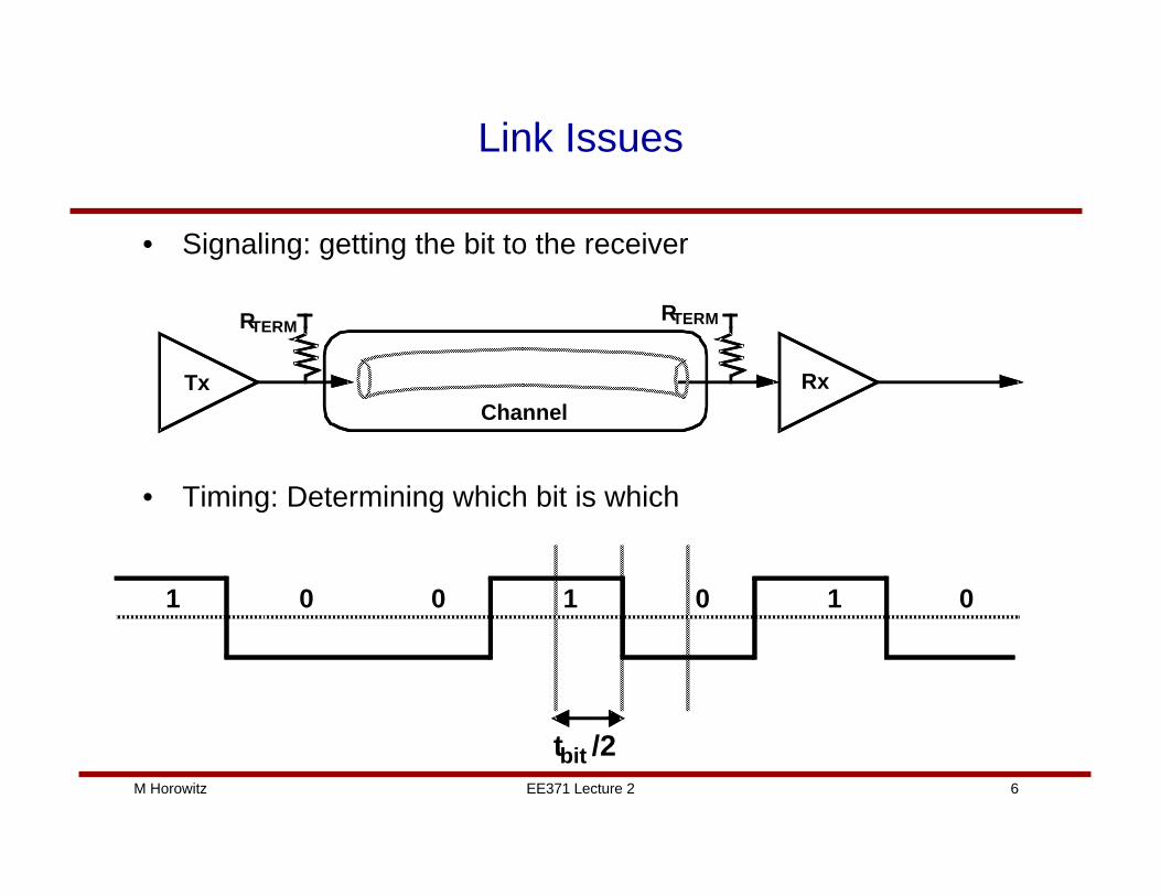
• Signaling: getting the bit to the receiver
• Timing: Determining which bit is which
RxTx
RTERM
Channel
RTERM
tbit /2
1 0 0 01 01
EE371 Lecture 2M Horowitz 7
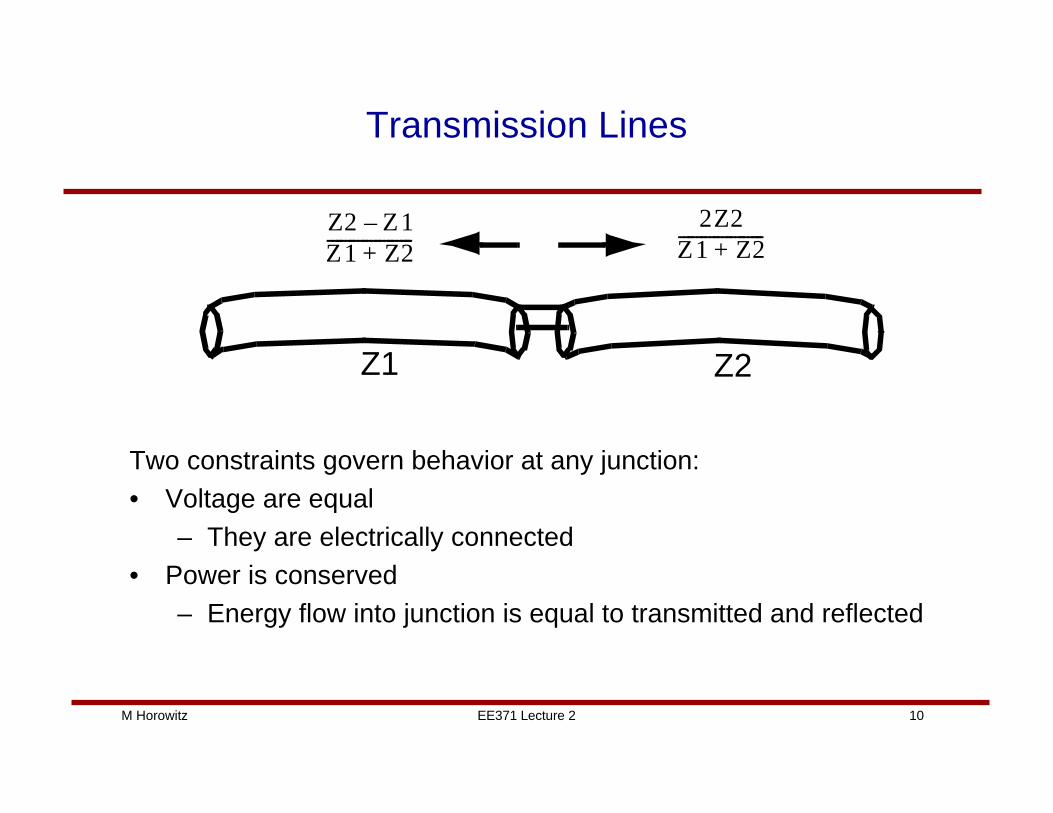
Transmission Lines
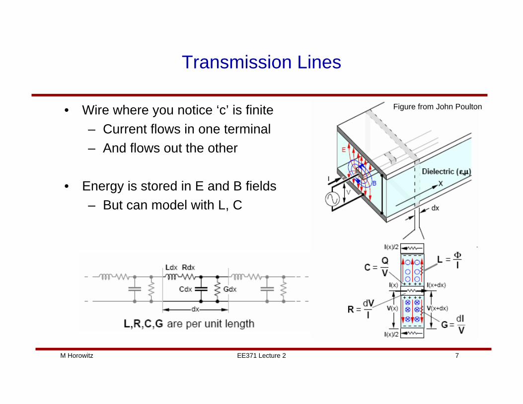
• Wire where you notice ‘c’ is finite– Current flows in one terminal– And flows out the other
• Energy is stored in E and B fields– But can model with L, C
Figure from John Poulton
EE371 Lecture 2M Horowitz 8
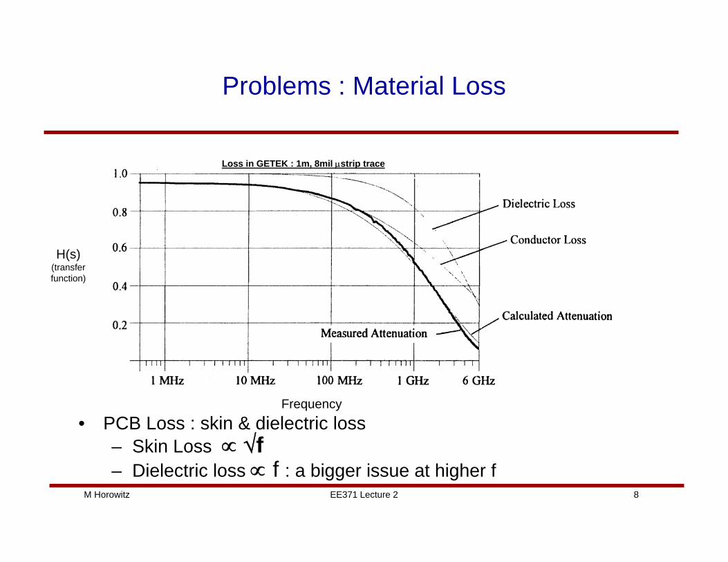
Problems : Material Loss
• PCB Loss : skin & dielectric loss– Skin Loss ∝ √f– Dielectric loss ∝ f : a bigger issue at higher f
H(s)(transferfunction)
Frequency
Loss in GETEK : 1m, 8mil μstrip trace
EE371 Lecture 2M Horowitz 9
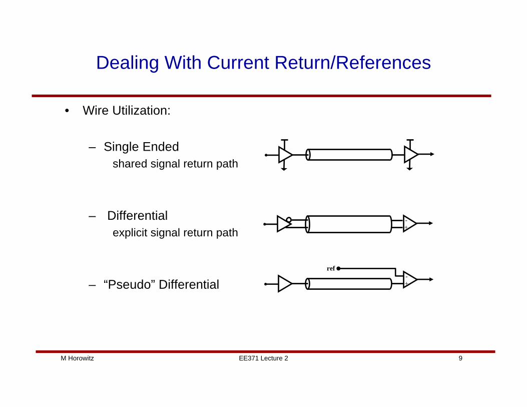
Dealing With Current Return/References
• Wire Utilization:
– Single Endedshared signal return path
– Differentialexplicit signal return path
– “Pseudo” Differential
+-
+-
ref
EE371 Lecture 2M Horowitz 10
Transmission Lines
Two constraints govern behavior at any junction:• Voltage are equal
– They are electrically connected• Power is conserved
– Energy flow into junction is equal to transmitted and reflected
Z1 Z2
Z2 Z1–Z1 Z2+--------------------
2Z2Z1 Z2+--------------------
EE371 Lecture 2M Horowitz 11
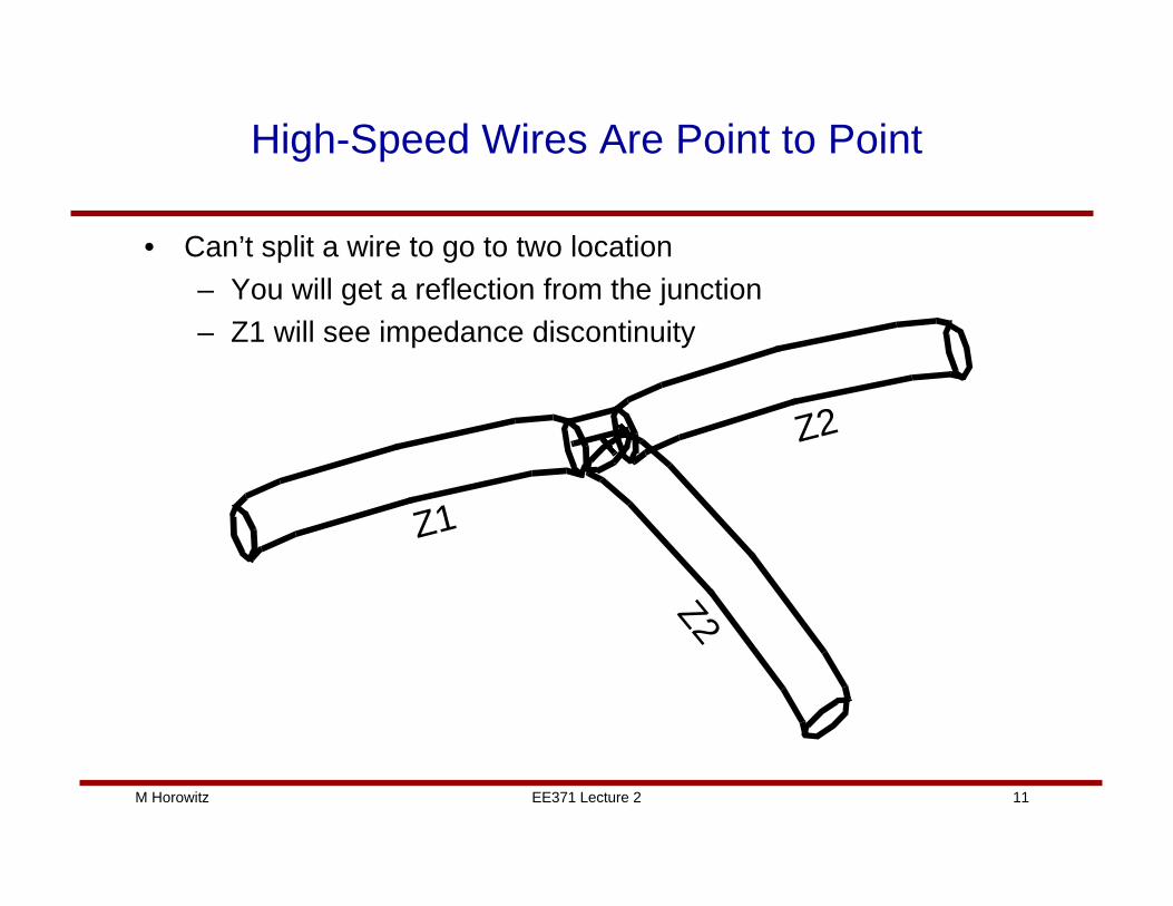
High-Speed Wires Are Point to Point
• Can’t split a wire to go to two location– You will get a reflection from the junction– Z1 will see impedance discontinuity
Z1
Z2Z2
EE371 Lecture 2M Horowitz 12
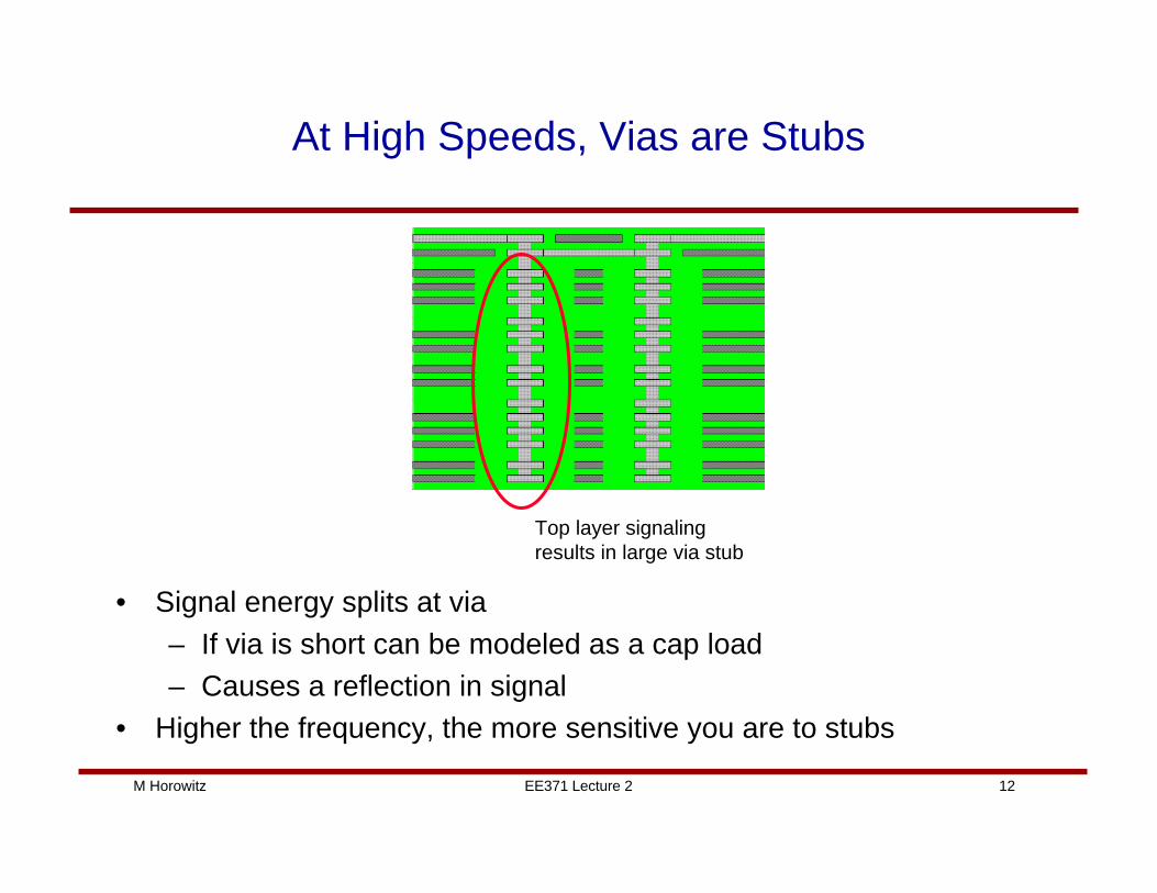
At High Speeds, Vias are Stubs
• Signal energy splits at via– If via is short can be modeled as a cap load– Causes a reflection in signal
• Higher the frequency, the more sensitive you are to stubs
Top layer signaling results in large via stub
EE371 Lecture 2M Horowitz 13
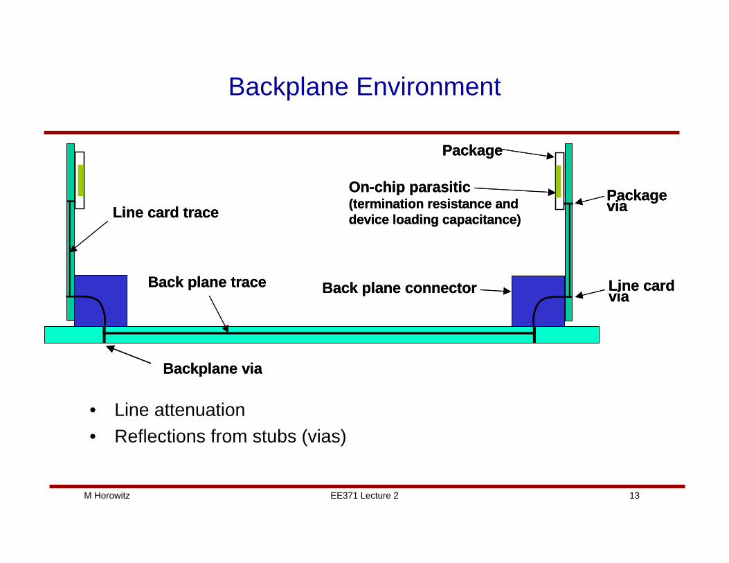
Backplane Environment
• Line attenuation• Reflections from stubs (vias)
Back plane connector
Line card trace
Package
On-chip parasitic(termination resistance and device loading capacitance)
Line card via
Back plane trace
Backplane via
Package via
Back plane connector
Line card trace
Package
On-chip parasitic(termination resistance and device loading capacitance)
Line card via
Back plane trace
Backplane via
Package via
EE371 Lecture 2M Horowitz 14
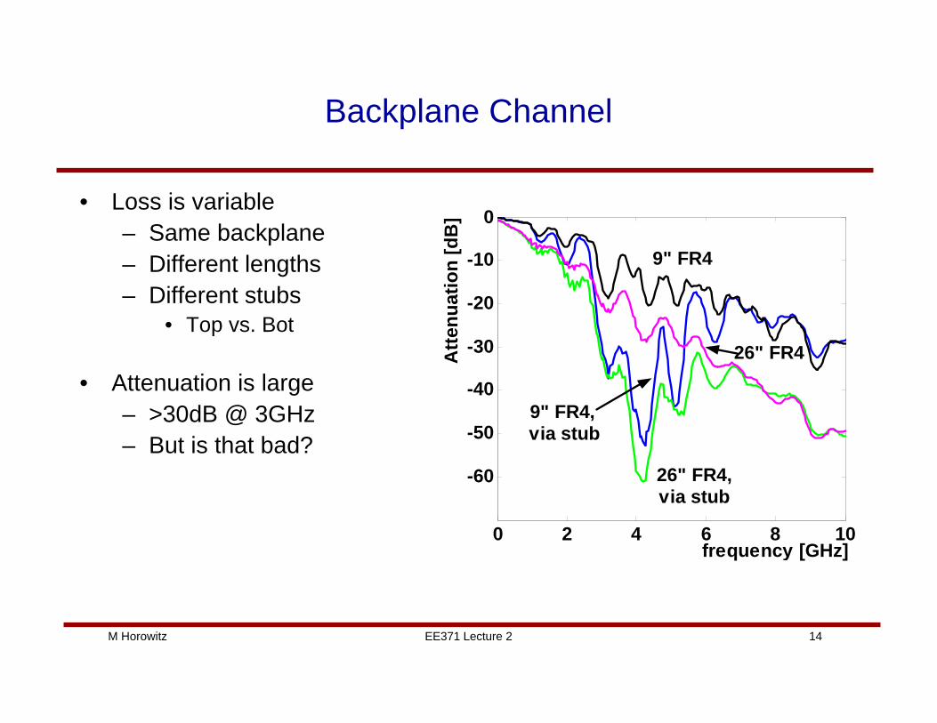
0 2 4 6 8 10
-60
-50
-40
-30
-20
-10
0
frequency [GHz]
Atte
nuat
ion
[dB
]
9" FR4, via stub
26" FR4,via stub
26" FR4
9" FR4
Backplane Channel
• Loss is variable– Same backplane– Different lengths– Different stubs
• Top vs. Bot
• Attenuation is large– >30dB @ 3GHz– But is that bad?
EE371 Lecture 2M Horowitz 15
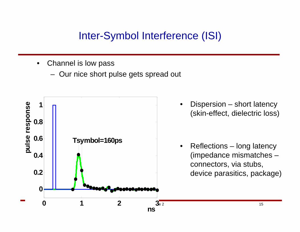
Inter-Symbol Interference (ISI)
• Channel is low pass– Our nice short pulse gets spread out
0 1 2 3
0
0.2
0.4
0.6
0.8
1
ns
puls
e re
spon
se
Tsymbol=160ps
• Dispersion – short latency (skin-effect, dielectric loss)
• Reflections – long latency (impedance mismatches –connectors, via stubs, device parasitics, package)
EE371 Lecture 2M Horowitz 16
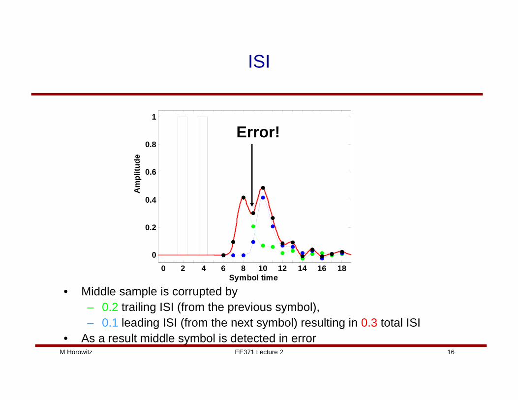
ISI
0 2 4 6 8 10 12 14 16 180
0.2
0.4
0.6
0.8
1
Symbol time
Am
plitu
deError!
• Middle sample is corrupted by – 0.2 trailing ISI (from the previous symbol), – 0.1 leading ISI (from the next symbol) resulting in 0.3 total ISI
• As a result middle symbol is detected in error
EE371 Lecture 2M Horowitz 17
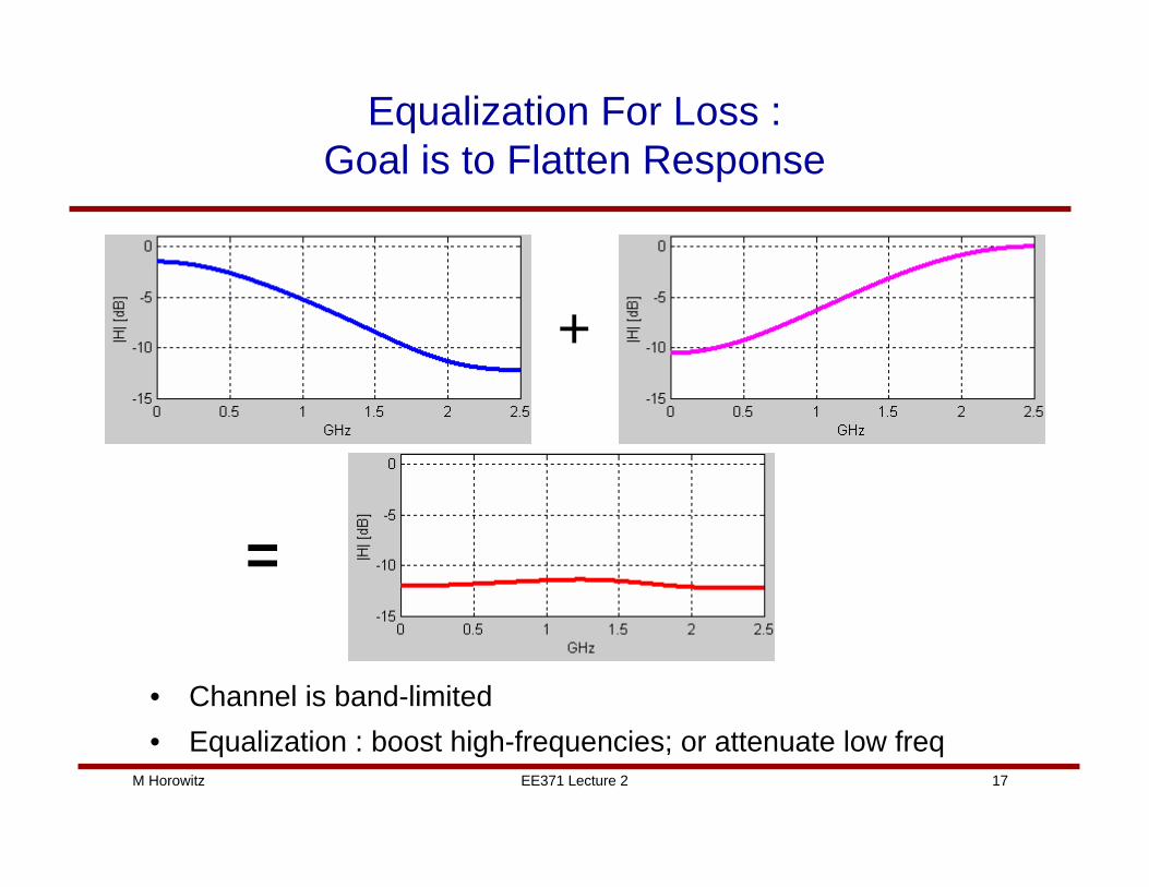
Equalization For Loss :Goal is to Flatten Response
• Channel is band-limited• Equalization : boost high-frequencies; or attenuate low freq
+
=
EE371 Lecture 2M Horowitz 18
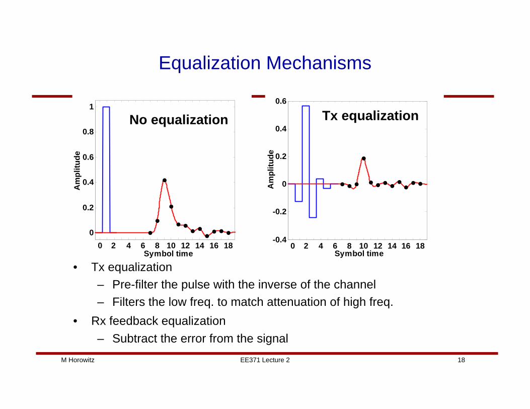
Equalization Mechanisms
0 2 4 6 8 10 12 14 16 180
0.2
0.4
0.6
0.8
1
Symbol time
Am
plitu
de
No equalization
0 2 4 6 8 10 12 14 16 18-0.4
-0.2
0
0.2
0.4
0.6
Symbol time
Am
plitu
de
Tx equalization
• Tx equalization– Pre-filter the pulse with the inverse of the channel– Filters the low freq. to match attenuation of high freq.
• Rx feedback equalization– Subtract the error from the signal
EE371 Lecture 2M Horowitz 19
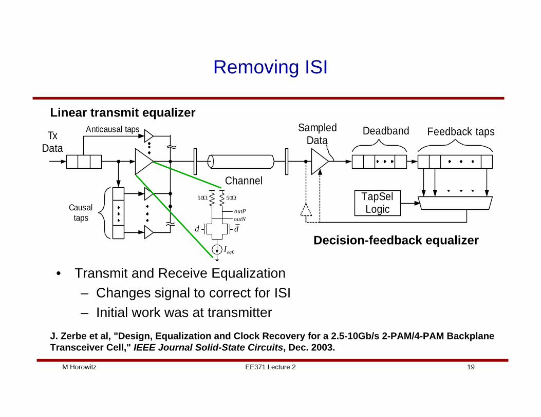
Removing ISI
• Transmit and Receive Equalization – Changes signal to correct for ISI– Initial work was at transmitter
Linear transmit equalizer
Decision-feedback equalizer
SampledData
Deadband Feedback taps
Tap SelLogic
TxData
Causaltaps
Anticausal taps
Channel
J. Zerbe et al, "Design, Equalization and Clock Recovery for a 2.5-10Gb/s 2-PAM/4-PAM Backplane Transceiver Cell," IEEE Journal Solid-State Circuits, Dec. 2003.
0eqI
doutNoutP
d
Ω50Ω50
EE371 Lecture 2M Horowitz 20
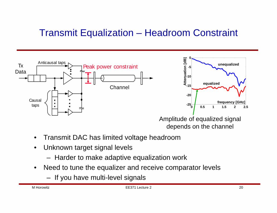
Transmit Equalization – Headroom Constraint
• Transmit DAC has limited voltage headroom• Unknown target signal levels
– Harder to make adaptive equalization work• Need to tune the equalizer and receive comparator levels
– If you have multi-level signals
0 0.5 1 1.5 2 2.5-25
-20
-15
-10
-5
0
frequency [GHz]
Atte
nuat
ion
[dB
]
equalized
unequalized
Amplitude of equalized signaldepends on the channel
TxData
Causaltaps
Anticausal taps
Channel
Peak power constraint
EE371 Lecture 2M Horowitz 21
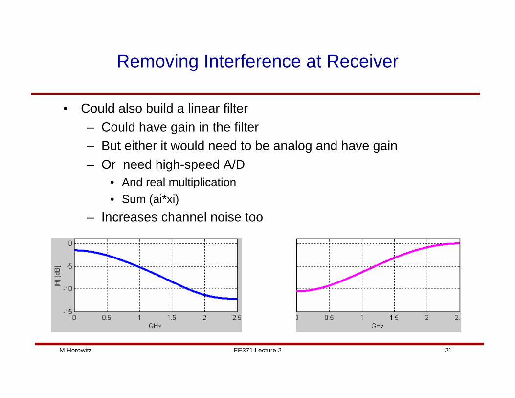
Removing Interference at Receiver
• Could also build a linear filter– Could have gain in the filter– But either it would need to be analog and have gain – Or need high-speed A/D
• And real multiplication• Sum (ai*xi)
– Increases channel noise too
EE371 Lecture 2M Horowitz 22
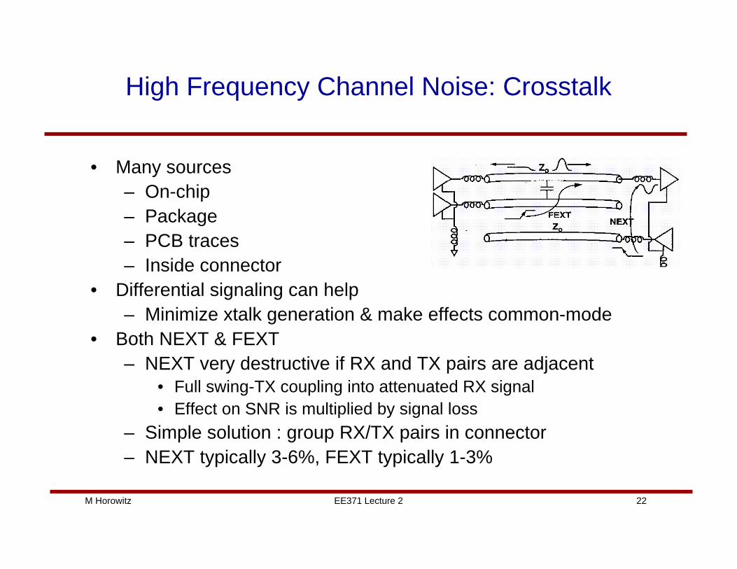
High Frequency Channel Noise: Crosstalk
• Many sources– On-chip– Package– PCB traces– Inside connector
• Differential signaling can help– Minimize xtalk generation & make effects common-mode
• Both NEXT & FEXT– NEXT very destructive if RX and TX pairs are adjacent
• Full swing-TX coupling into attenuated RX signal• Effect on SNR is multiplied by signal loss
– Simple solution : group RX/TX pairs in connector– NEXT typically 3-6%, FEXT typically 1-3%
EE371 Lecture 2M Horowitz 23
0 2 4 6 8 10 12 14 16 180
0.2
0.4
0.6
0.8
1
Symbol time
Am
plitu
de
Feedbackequalization
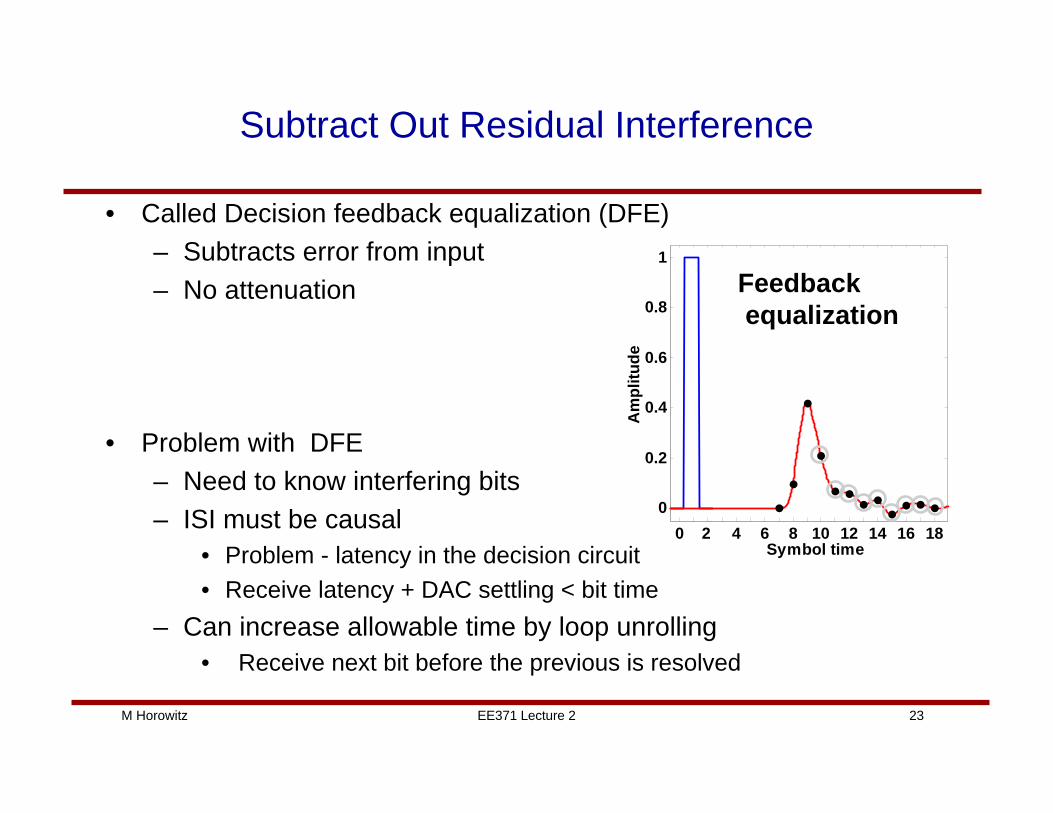
Subtract Out Residual Interference
• Called Decision feedback equalization (DFE)– Subtracts error from input – No attenuation
• Problem with DFE– Need to know interfering bits– ISI must be causal
• Problem - latency in the decision circuit• Receive latency + DAC settling < bit time
– Can increase allowable time by loop unrolling• Receive next bit before the previous is resolved

EE371 Lecture 2M Horowitz 24
Removing ISI
• Transmit and Receive Equalization – Changes signal to correct for ISI– Initial work was at transmitter
Linear transmit equalizer
Decision-feedback equalizer
SampledData
Deadband Feedback taps
Tap SelLogic
TxData
Causaltaps
Anticausal taps
Channel
J. Zerbe et al, "Design, Equalization and Clock Recovery for a 2.5-10Gb/s 2-PAM/4-PAM Backplane Transceiver Cell," IEEE Journal Solid-State Circuits, Dec. 2003.
0eqI
doutNoutP
d
Ω50Ω50
EE371 Lecture 2M Horowitz 25
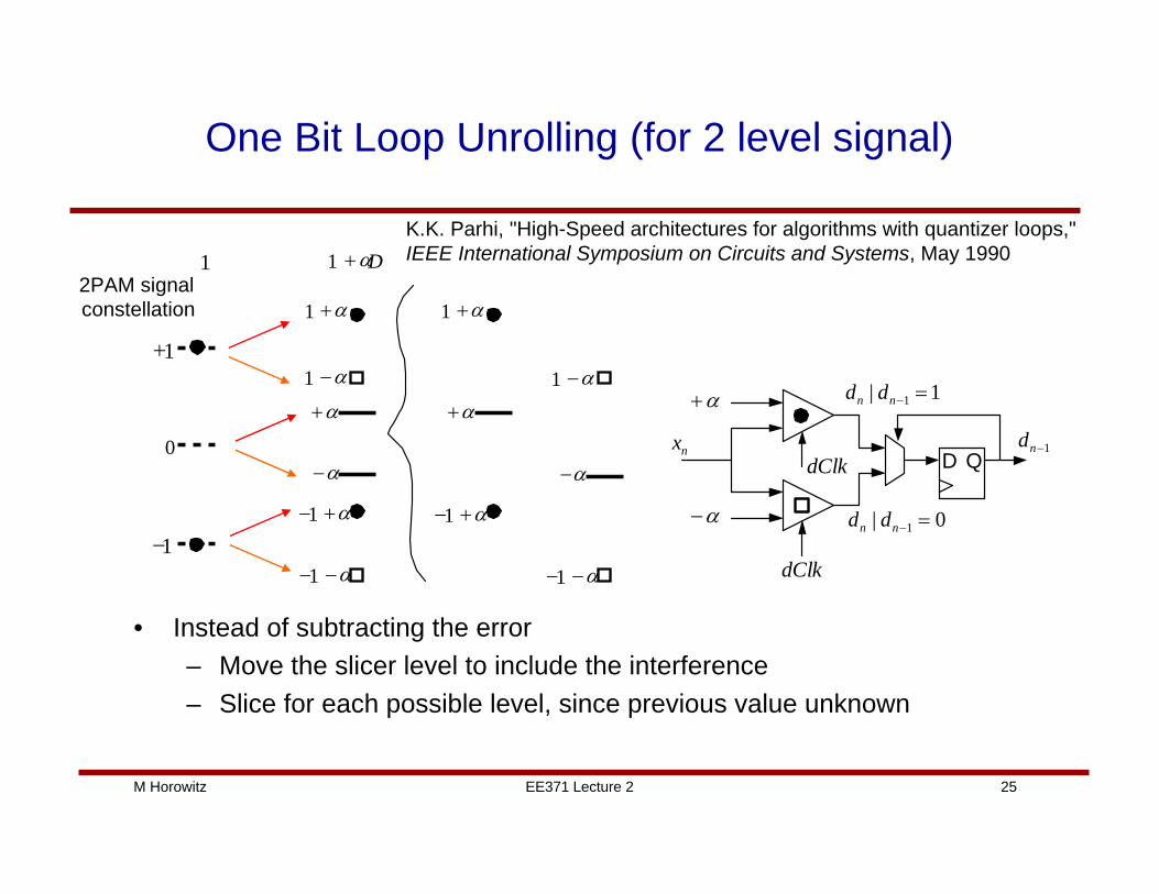
One Bit Loop Unrolling (for 2 level signal)
• Instead of subtracting the error– Move the slicer level to include the interference– Slice for each possible level, since previous value unknown
K.K. Parhi, "High-Speed architectures for algorithms with quantizer loops," IEEE International Symposium on Circuits and Systems, May 1990
D Q1−nd
dClk
1| 1 =−nn dd
0| 1 =−nn ddα−
dClk
α+
nx
1+
1−
α+1
α−1
α+−1
α−−1
α+
α−0
2PAM signalconstellation
1 Dα+1
α+1
α+
α−1
α−
α+−1
α−−1
EE371 Lecture 2M Horowitz 26
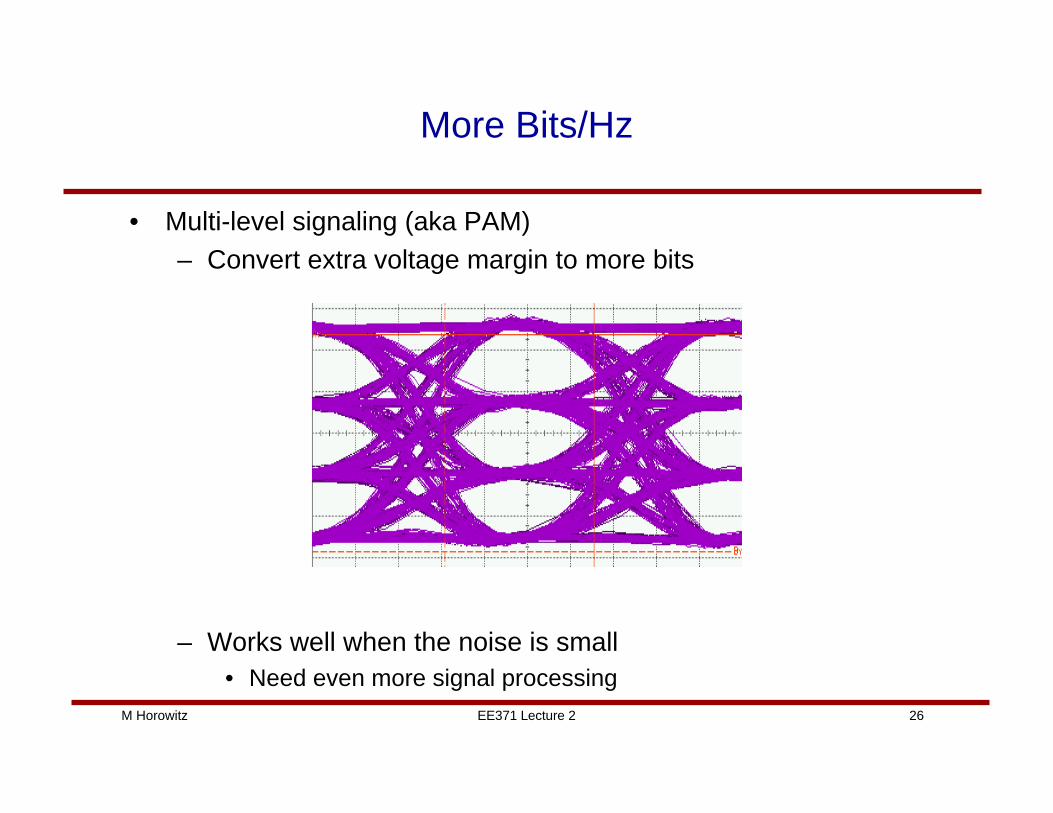
More Bits/Hz
• Multi-level signaling (aka PAM)– Convert extra voltage margin to more bits
– Works well when the noise is small• Need even more signal processing
EE371 Lecture 2M Horowitz 27
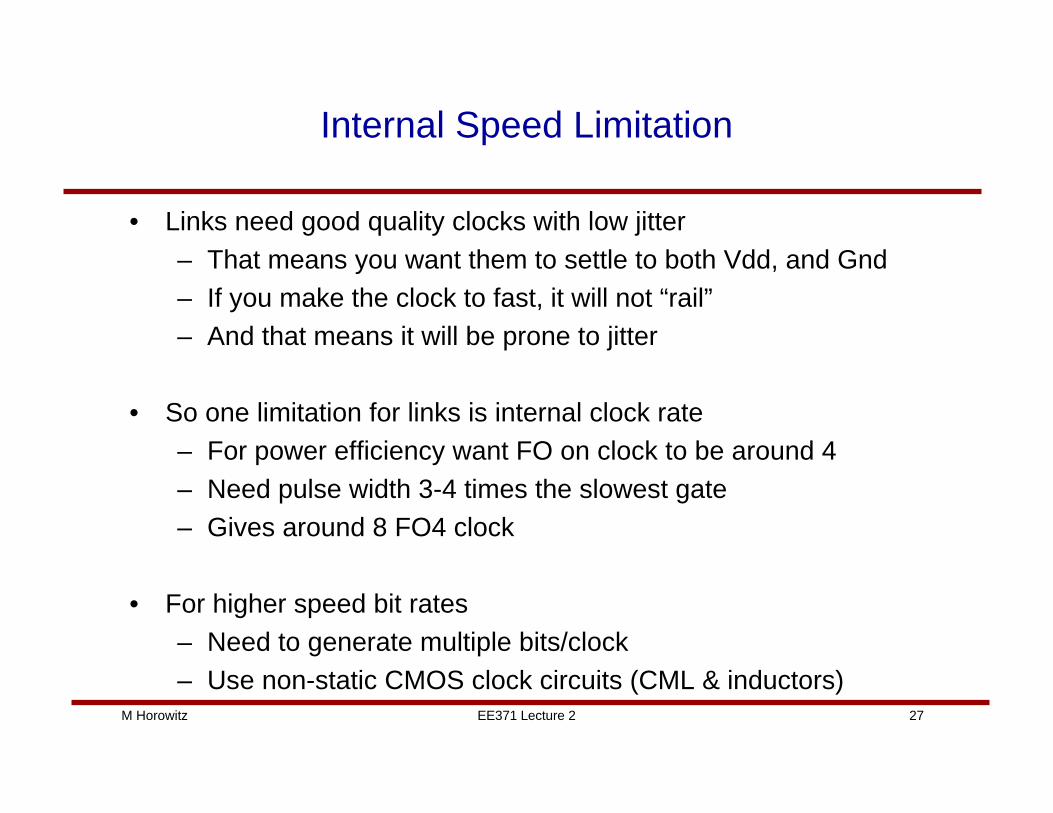
Internal Speed Limitation
• Links need good quality clocks with low jitter– That means you want them to settle to both Vdd, and Gnd– If you make the clock to fast, it will not “rail”– And that means it will be prone to jitter
• So one limitation for links is internal clock rate– For power efficiency want FO on clock to be around 4– Need pulse width 3-4 times the slowest gate– Gives around 8 FO4 clock
• For higher speed bit rates– Need to generate multiple bits/clock– Use non-static CMOS clock circuits (CML & inductors)
EE371 Lecture 2M Horowitz 28
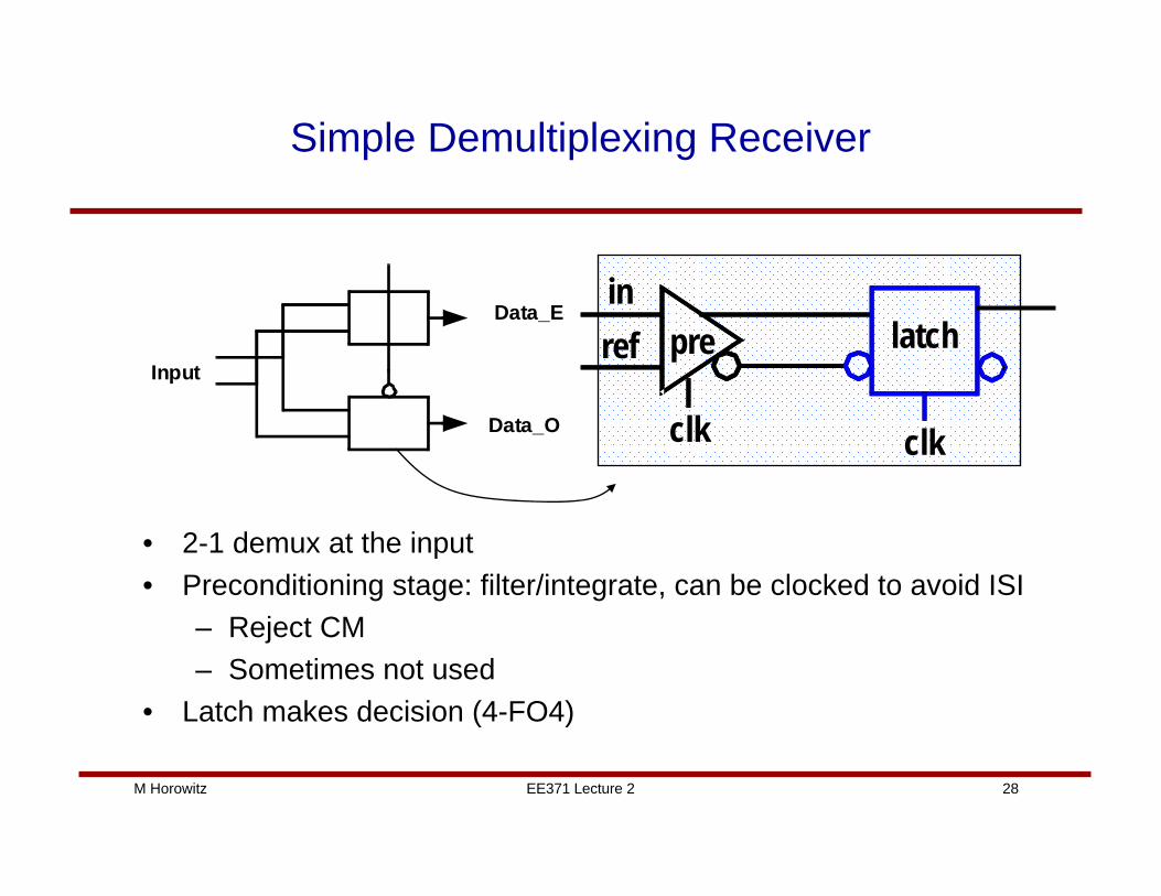
Simple Demultiplexing Receiver
• 2-1 demux at the input• Preconditioning stage: filter/integrate, can be clocked to avoid ISI
– Reject CM– Sometimes not used
• Latch makes decision (4-FO4)
Data_E
Data_O
Input
inref
clk
pre latch
clk
EE371 Lecture 2M Horowitz 29
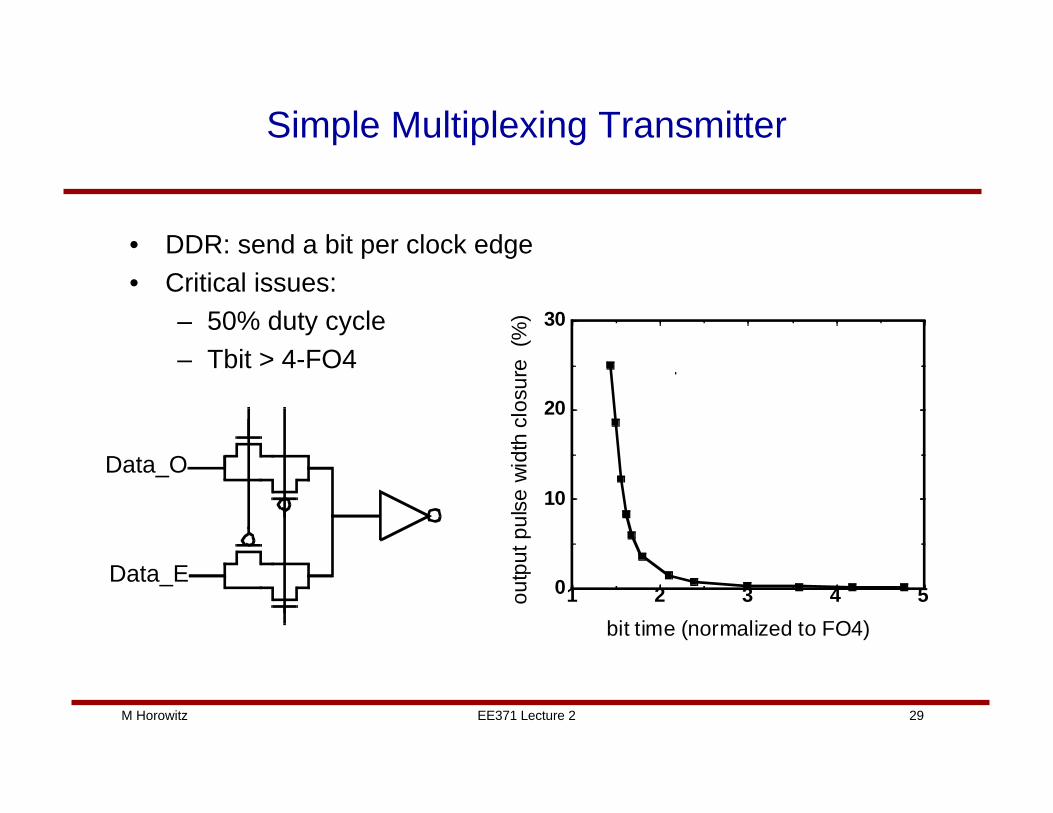
Simple Multiplexing Transmitter
• DDR: send a bit per clock edge• Critical issues:
– 50% duty cycle– Tbit > 4-FO4
Data_O
Data_E1 2 3 4 50
10
20
30
bit time (normalized to FO4)
outp
ut p
ulse
wid
th c
losu
re (
%)
EE371 Lecture 2M Horowitz 30
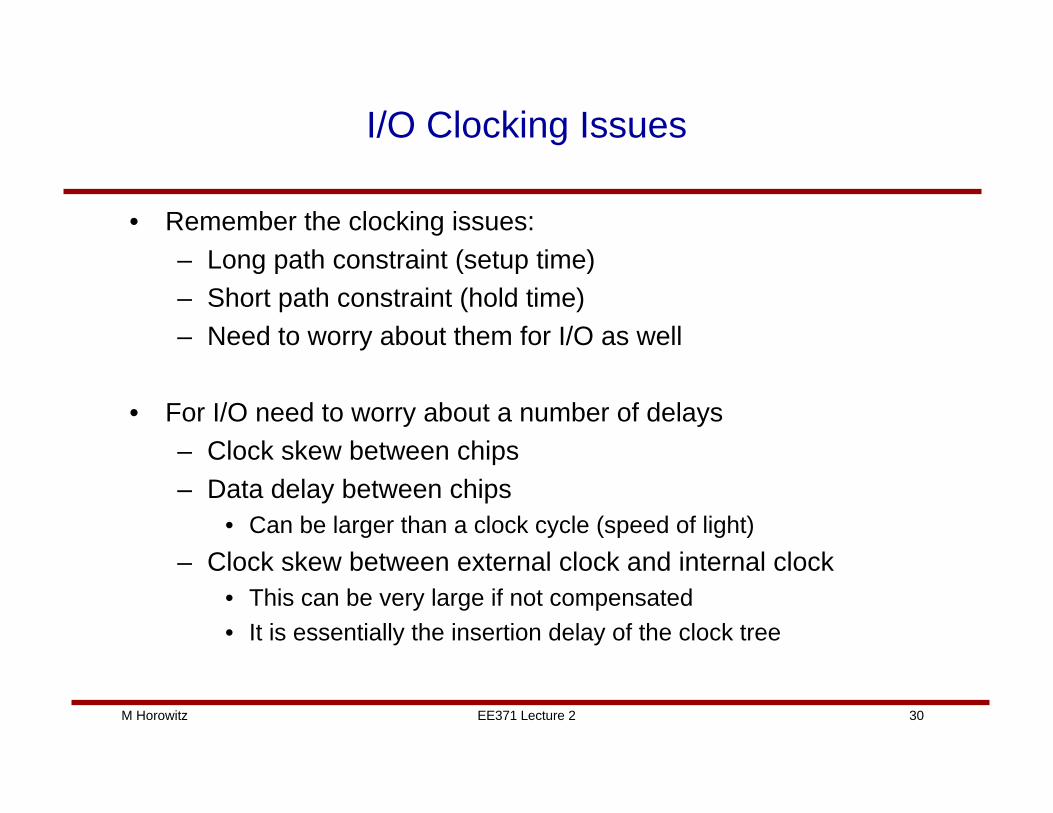
I/O Clocking Issues
• Remember the clocking issues:– Long path constraint (setup time)– Short path constraint (hold time)– Need to worry about them for I/O as well
• For I/O need to worry about a number of delays– Clock skew between chips– Data delay between chips
• Can be larger than a clock cycle (speed of light)– Clock skew between external clock and internal clock
• This can be very large if not compensated• It is essentially the insertion delay of the clock tree
EE371 Lecture 2M Horowitz 31
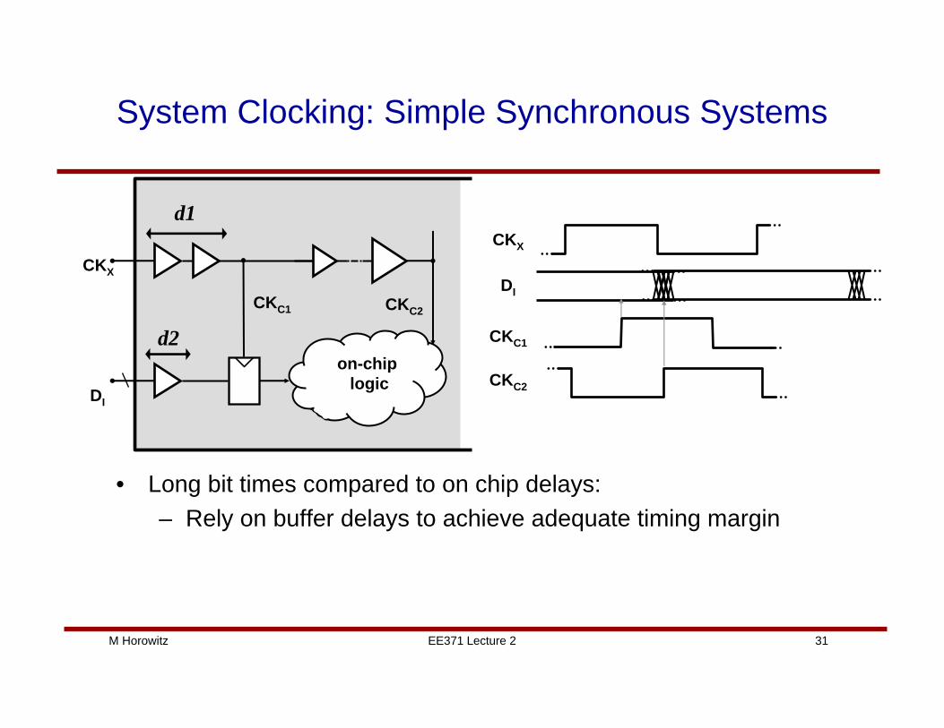
System Clocking: Simple Synchronous Systems
• Long bit times compared to on chip delays:– Rely on buffer delays to achieve adequate timing margin
CKX
CKC2
DI
on-chip logic
CKC1
CKX
DI
CKC1
CKC2
d1
d2
EE371 Lecture 2M Horowitz 32
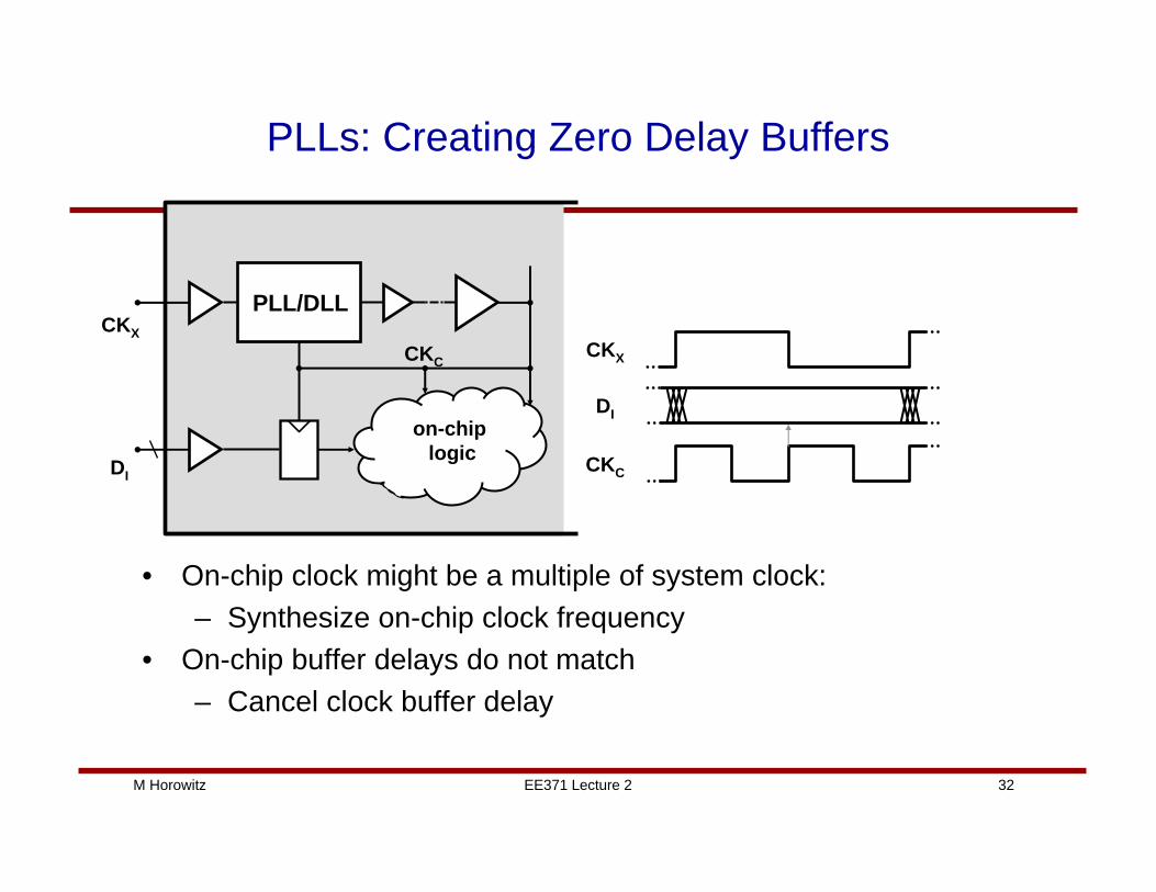
PLLs: Creating Zero Delay Buffers
• On-chip clock might be a multiple of system clock:– Synthesize on-chip clock frequency
• On-chip buffer delays do not match– Cancel clock buffer delay
PLL/DLLCKX
CKC
DI
CKX
DI
CKC
on-chip logic
EE371 Lecture 2M Horowitz 33
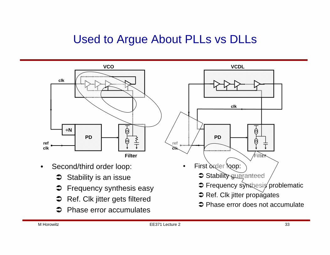
Used to Argue About PLLs vs DLLs
• Second/third order loop:Stability is an issueFrequency synthesis easyRef. Clk jitter gets filteredPhase error accumulates
• First order loop:Stability guaranteedFrequency synthesis problematicRef. Clk jitter propagatesPhase error does not accumulate
÷NPD
refclk
VCO
Filter
PDrefclk
VCDL
Filter
clk
clk
EE371 Lecture 2M Horowitz 34
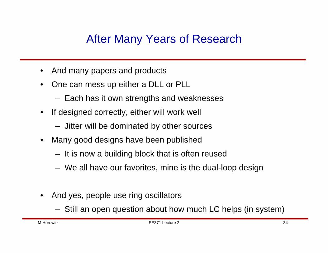
After Many Years of Research
• And many papers and products
• One can mess up either a DLL or PLL
– Each has it own strengths and weaknesses
• If designed correctly, either will work well
– Jitter will be dominated by other sources
• Many good designs have been published
– It is now a building block that is often reused
– We all have our favorites, mine is the dual-loop design
• And yes, people use ring oscillators
– Still an open question about how much LC helps (in system)
EE371 Lecture 2M Horowitz 35
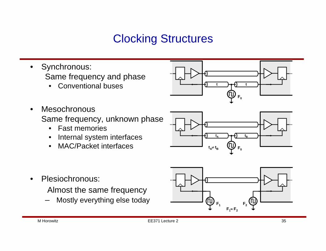
Clocking Structures
• Synchronous:Same frequency and phase• Conventional buses
• MesochronousSame frequency, unknown phase
• Fast memories• Internal system interfaces• MAC/Packet interfaces
• Plesiochronous:Almost the same frequency
– Mostly everything else today
t t
F0
tA tB
F0tA≠ tB
F1 F2F1≈ F2
EE371 Lecture 2M Horowitz 36
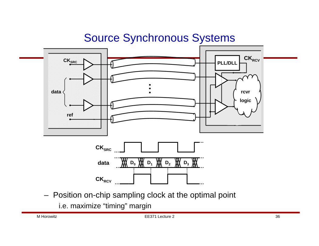
Source Synchronous Systems
– Position on-chip sampling clock at the optimal pointi.e. maximize “timing” margin
PLL/DLL
ref
data
CKSRC
rcvr
logic
CKRCV
CKSRC
data
CKRCV
D0 D1 D2 D3
EE371 Lecture 2M Horowitz 37
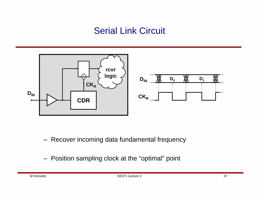
Serial Link Circuit
– Recover incoming data fundamental frequency
– Position sampling clock at the “optimal” point
DINCDR
CKR
rcvrlogic D0 D1DIN
CKR