Introduction to Engineering Materials ENGR2000...
69
Introduction to Engineering Materials ENGR2000 Chapter 18: Electrical Properties Chapter 18: Electrical Properties Dr.Coates
Transcript of Introduction to Engineering Materials ENGR2000...
Introduction to Engineering Materials
ENGR2000
Chapter 18: Electrical PropertiesChapter 18: Electrical Properties
Dr.Coates
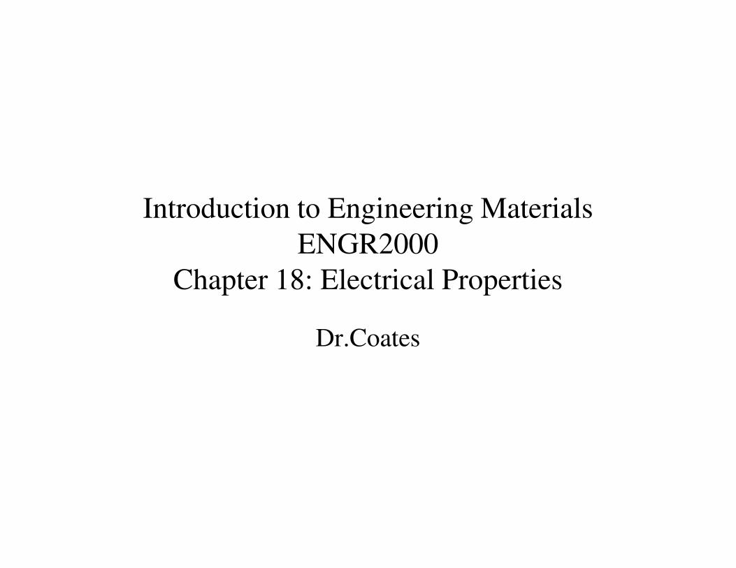
18.2 Ohm’s Law
current. theis and voltage theis
material, theof resistance theis R where
lR
IV
IRV
∝
=
section.-cross of area theis
andspecimen theoflength theis
material, theofy resistivit theis where
A
l
A
lR
A
lR
ρ
ρ=⇒
∝
Measurement of Electrical
Resistivity
Recall from Physics 2211
• What are units for I, V, R?
Does voltage flow through a
material? Why/why not?
Units of ρ?
Does shape of cross-section
affect ρ?
18.3 Electrical Conductivity
• The ease with which a material is capable of
conducting an electrical current.
1σ =
material. theofty conductivi electrical theis where
1
σ
ρσ =
Units of σ?
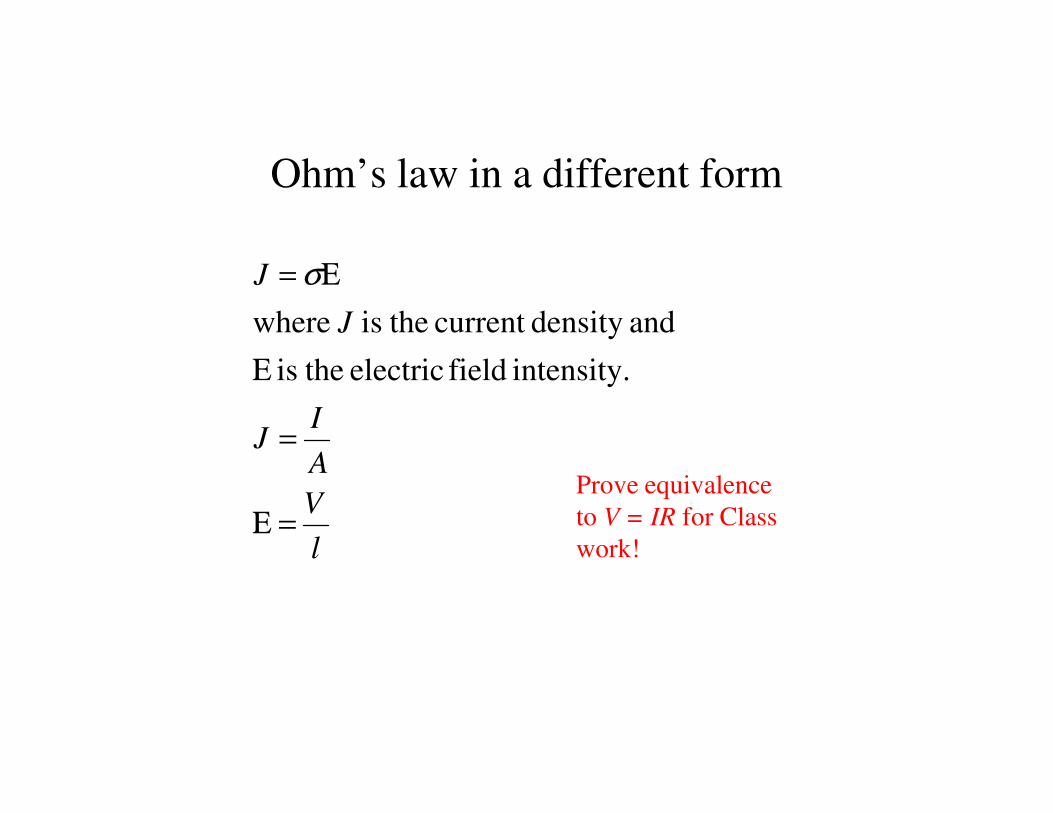
Ohm’s law in a different form
I
J
J
Ε
Ε=
intensity. field electric theis
anddensity current theis where
σ
l
V
A
IJ
=Ε
=
Prove equivalence
to V = IR for Class
work!
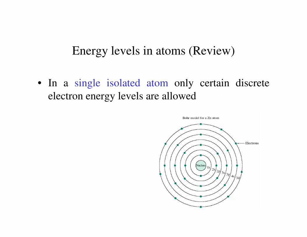
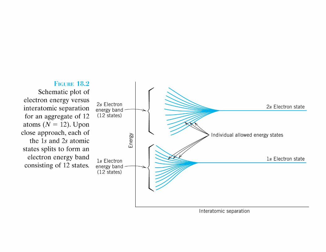
Energy levels in atoms (Review)
• In a single isolated atom only certain discrete
electron energy levels are allowed
18.5 Energy Band Structures in Solids
• As atoms are brought close together, the electrons
are perturbed by the electrons and nuclei of
adjacent atoms.
• Each atomic state is split into a series of closely• Each atomic state is split into a series of closely
spaced electron states in the solid – electron
energy band
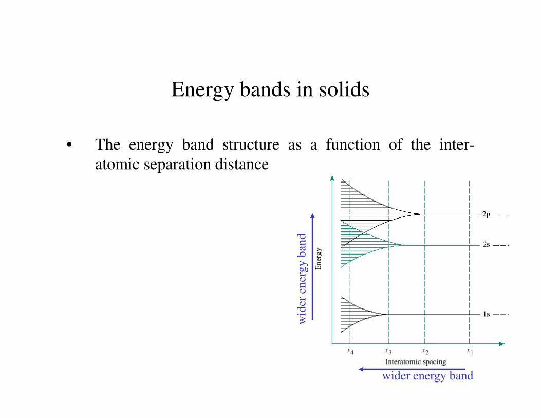
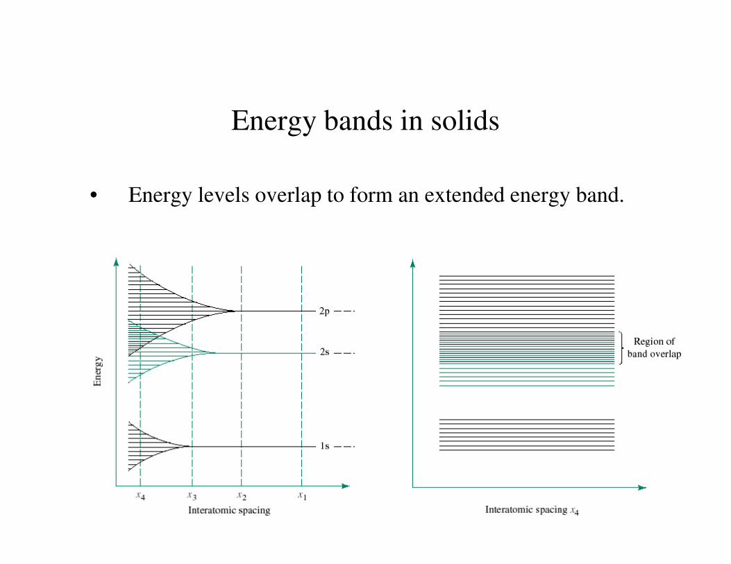
Energy bands in solids
• The energy band structure as a function of the inter-
atomic separation distance
wider energy band
wid
eren
ergy
ban
d
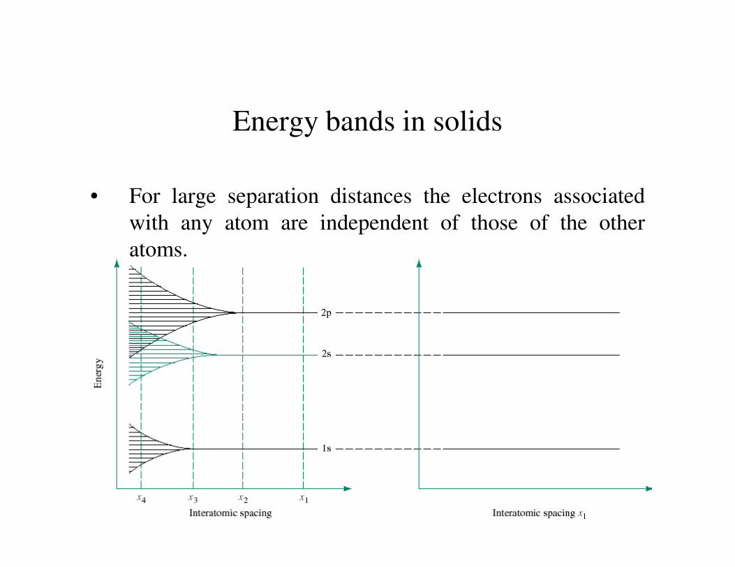
Energy bands in solids
• For large separation distances the electrons associated
with any atom are independent of those of the other
atoms.
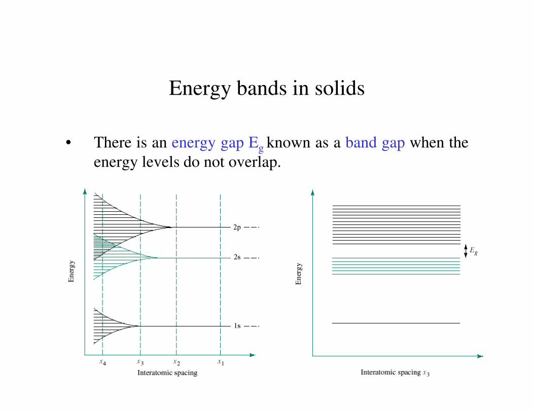
Energy bands in solids
• There is an energy gap Eg known as a band gap when the
energy levels do not overlap.
Energy bands in solids
• Energy levels overlap to form an extended energy band.
Four Types of Energy Bands
• Valence band – the highest energy band that is at least
partially occupied (eg. Fig 18.4c)
• Core bands – all the bands below the valence band
• Conduction band – the energy band above the valence• Conduction band – the energy band above the valence
band
• Band gap or energy gap – forbidden energy range
between the valence and conduction bands
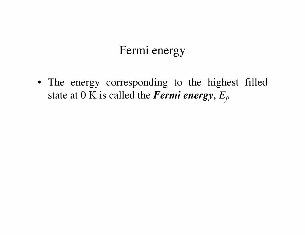
Fermi energy
• The energy corresponding to the highest filled
state at 0 K is called the Fermi energy, Ef.
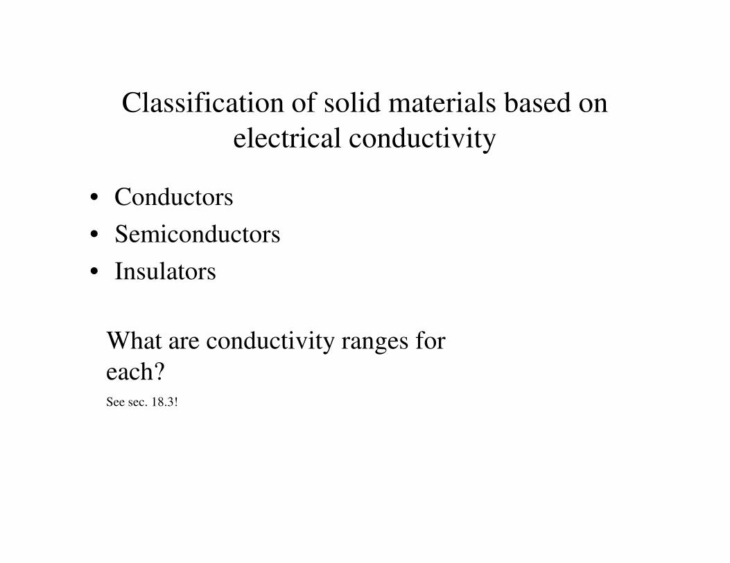
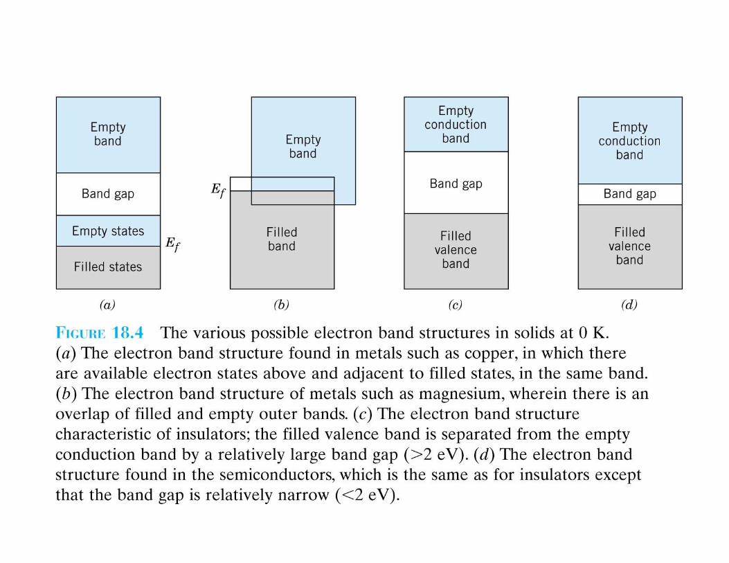
Classification of solid materials based on
electrical conductivity
• Conductors
• Semiconductors
• Insulators• Insulators
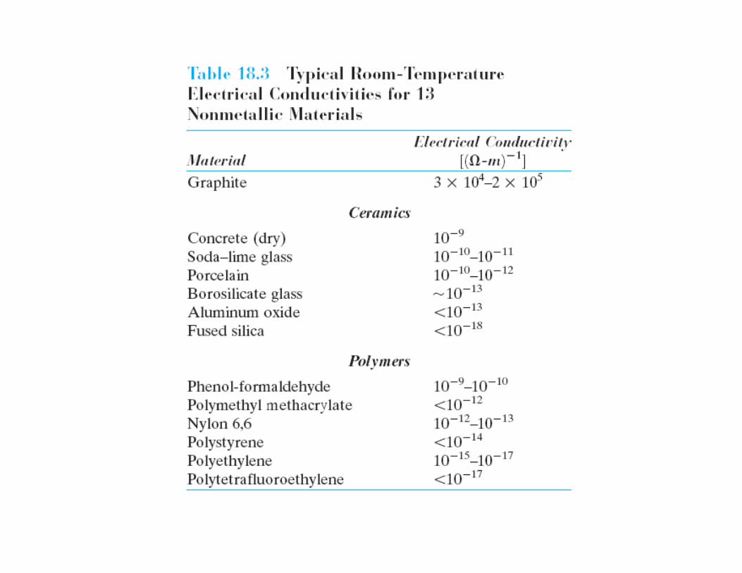
What are conductivity ranges for
each? See sec. 18.3!
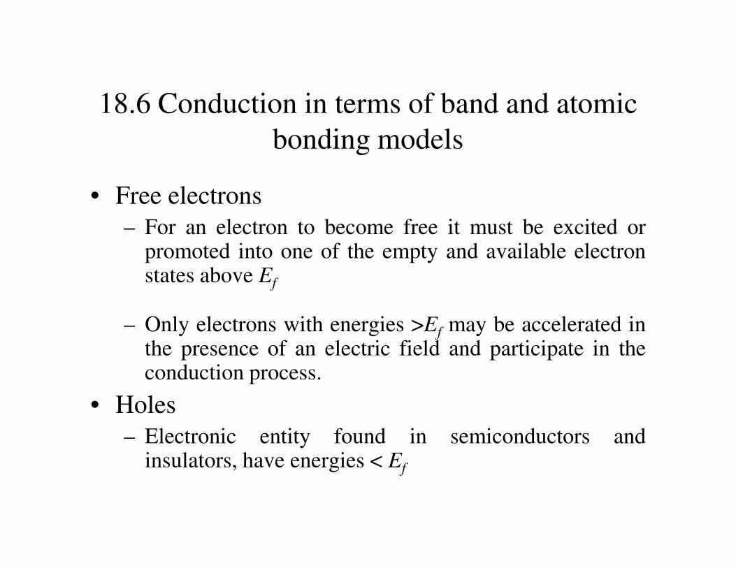
18.6 Conduction in terms of band and atomic
bonding models
• Free electrons
– For an electron to become free it must be excited orpromoted into one of the empty and available electronstates above Efstates above Ef
– Only electrons with energies >Ef may be accelerated inthe presence of an electric field and participate in theconduction process.
• Holes
– Electronic entity found in semiconductors andinsulators, have energies < Ef
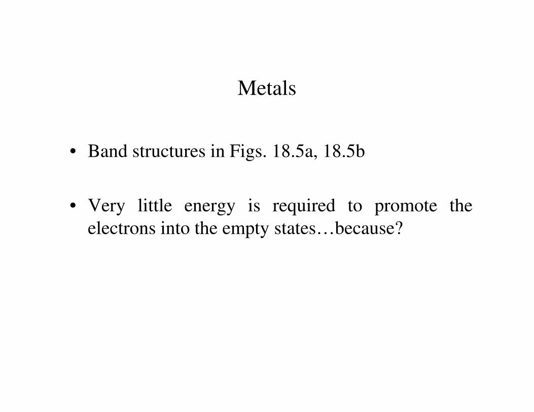
Metals
• Band structures in Figs. 18.5a, 18.5b
• Very little energy is required to promote the• Very little energy is required to promote the
electrons into the empty states…because?
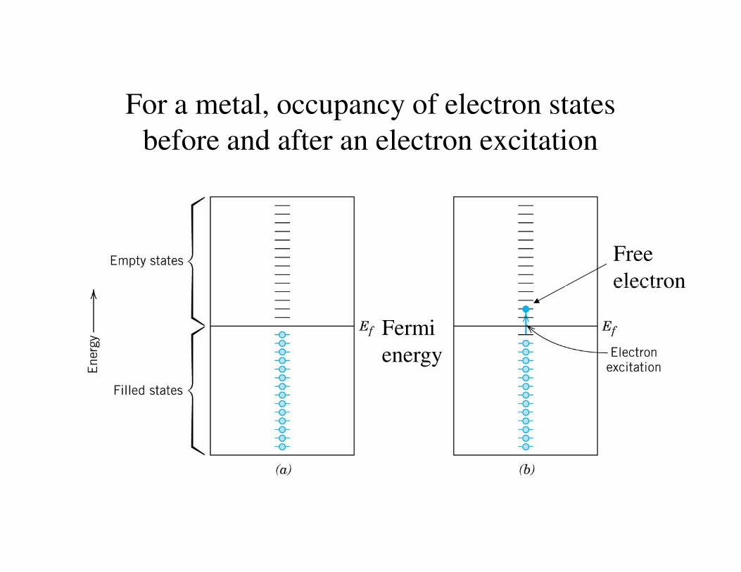
For a metal, occupancy of electron states
before and after an electron excitation
Free
electron
Fermi
energy
electron
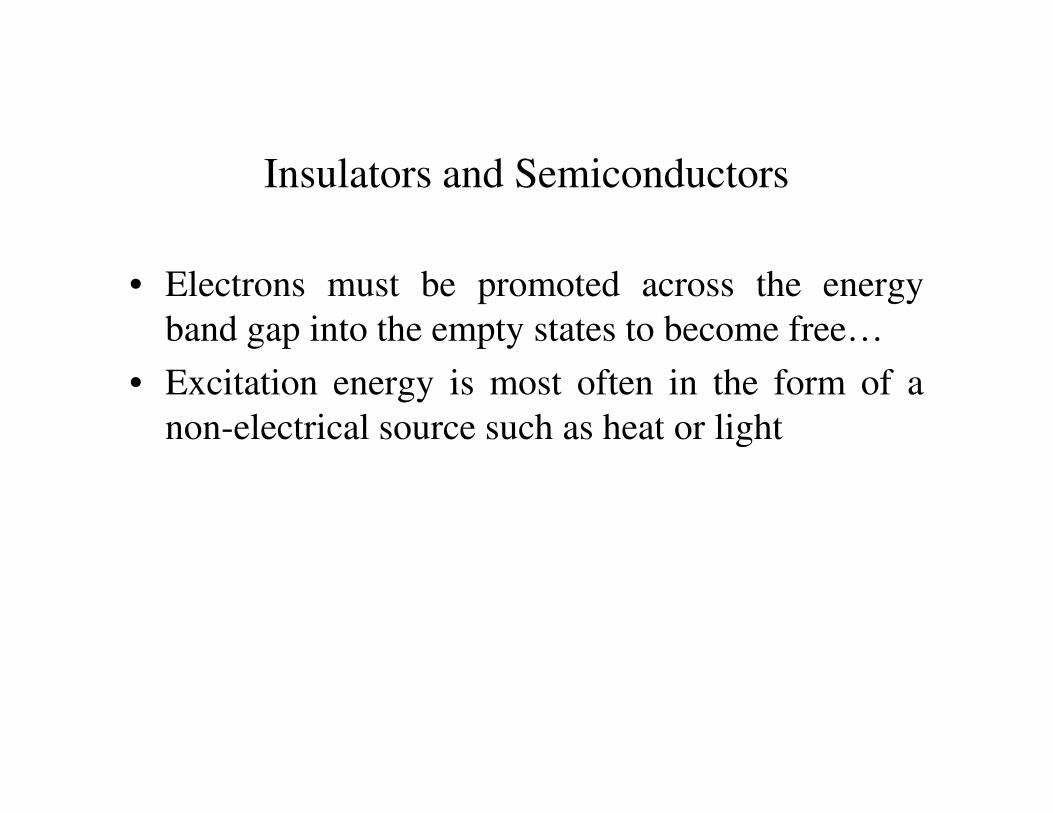
Insulators and Semiconductors
• Electrons must be promoted across the energy
band gap into the empty states to become free…
• Excitation energy is most often in the form of a
non-electrical source such as heat or lightnon-electrical source such as heat or light
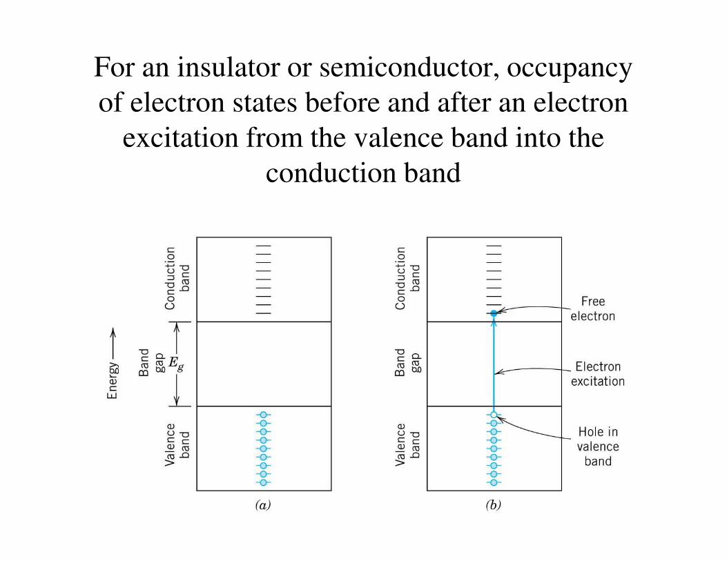
For an insulator or semiconductor, occupancy
of electron states before and after an electron
excitation from the valence band into the
conduction band
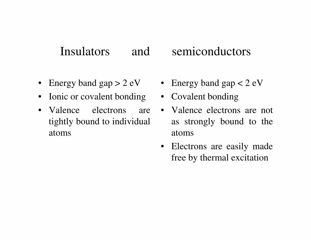
Insulators and semiconductors
• Energy band gap > 2 eV
• Ionic or covalent bonding
• Valence electrons are
tightly bound to individual
• Energy band gap < 2 eV
• Covalent bonding
• Valence electrons are not
as strongly bound to thetightly bound to individual
atoms
as strongly bound to the
atoms
• Electrons are easily made
free by thermal excitation
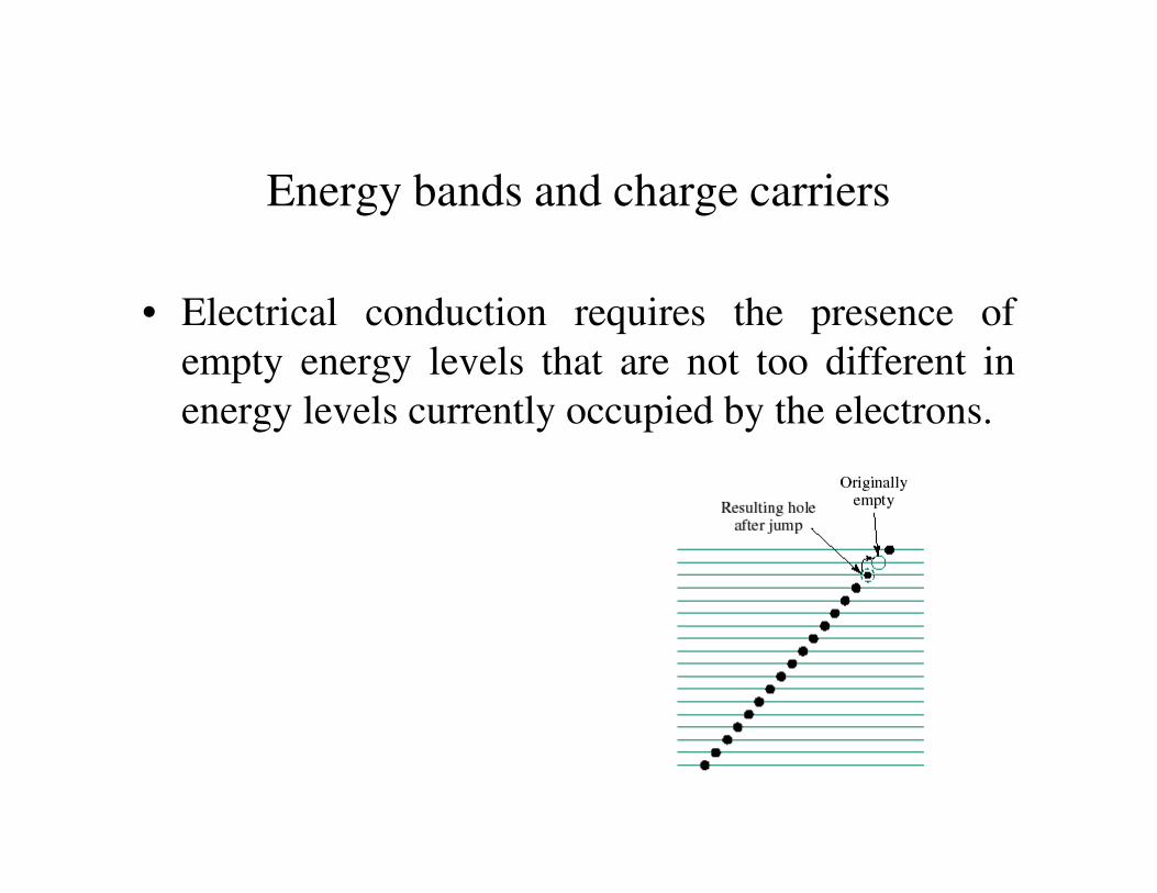
Energy bands and charge carriers
• Electrical conduction requires the presence of
empty energy levels that are not too different in
energy levels currently occupied by the electrons.
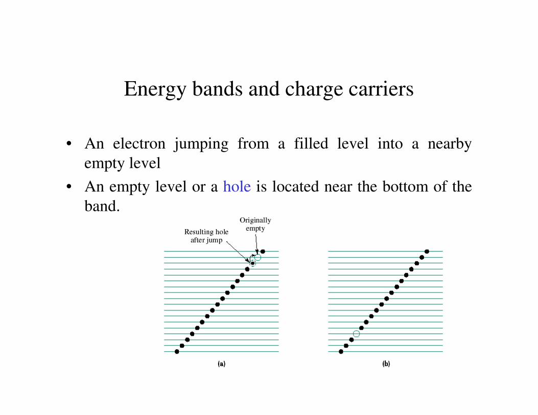
Energy bands and charge carriers
• An electron jumping from a filled level into a nearby
empty level
• An empty level or a hole is located near the bottom of the
band.band.
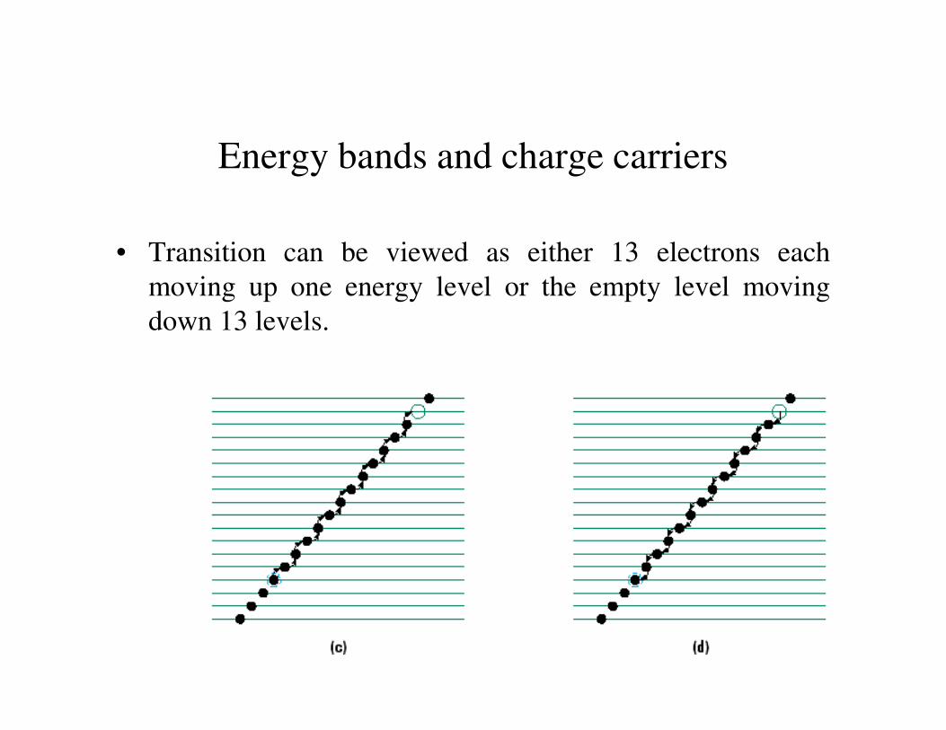
Energy bands and charge carriers
• Transition can be viewed as either 13 electrons each
moving up one energy level or the empty level moving
down 13 levels.
18.7 Electron Mobility
• The ease with which the free electrons movethrough the solid in response to an electric field.
• Electric field => force on electron
• Why doesn’t electron continually accelerate?• Why doesn’t electron continually accelerate?
Frictional forces-scattering of electrons due to
imperfections in crystal lattice, impurity
atoms,vacancies, interstitial atoms, dislocations, thermal
vibrations
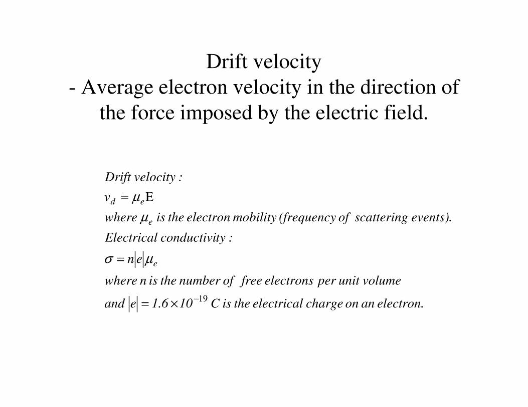
Drift velocity
- Average electron velocity in the direction of
the force imposed by the electric field.
v
:velocity Drift
ed Ε= µ
electron. an on charge electrical the is C101.6e and
volume unit per electrons free of number the is n where
en
:tyconductivi Electrical
events). g scatterinof (frequencymobility electron the is where
v
e
e
ed
19−×=
=
Ε=
µσ
µ
µ
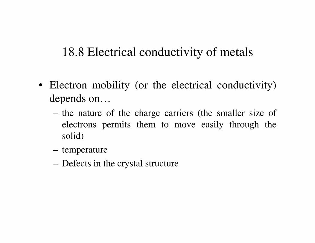
18.8 Electrical conductivity of metals
• Electron mobility (or the electrical conductivity)
depends on…
– the nature of the charge carriers (the smaller size of
electrons permits them to move easily through theelectrons permits them to move easily through the
solid)
– temperature
– Defects in the crystal structure
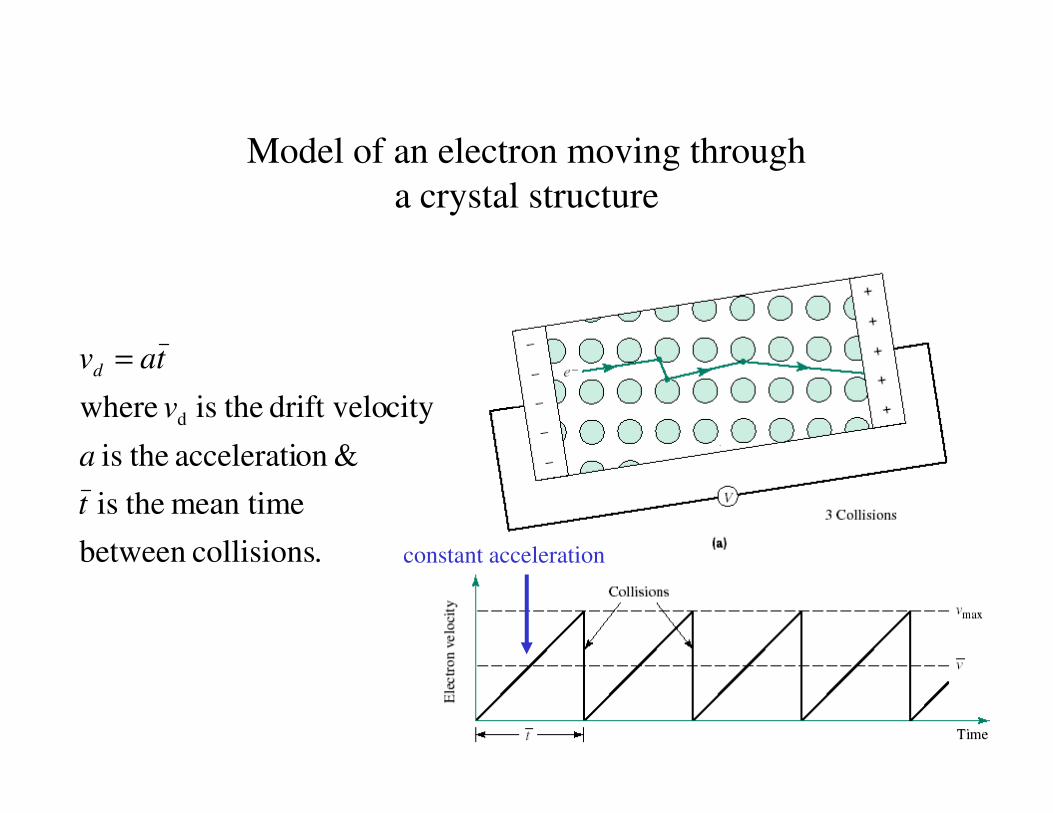
Model of an electron moving through
a crystal structure
citydrift velo theis where v
tavd =
constant acceleration
.collisionsbetween
mean time theis
&onaccelerati theis
citydrift velo theis where d
t
a
v
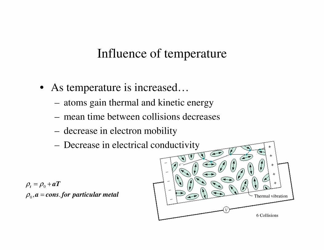
Influence of temperature
• As temperature is increased…
– atoms gain thermal and kinetic energy
– mean time between collisions decreases
– decrease in electron mobility– decrease in electron mobility
– Decrease in electrical conductivity
metalparticularforconsa
aTt
.,0
0
=
+=
ρ
ρρ
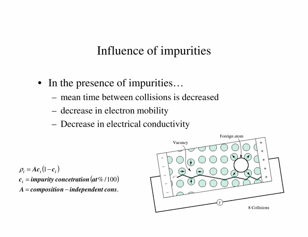
Influence of impurities
• In the presence of impurities…
– mean time between collisions is decreased
– decrease in electron mobility
– Decrease in electrical conductivity– Decrease in electrical conductivity
( )( )
.
100/%
1
constindependenncompositioA
atonconcetratiimpurityc
cAc
i
iii
−=
=
−=ρ
• For a two-phase alloy
ρρρρ ++=
.resindividual
fractionvolumeV
VV
s
s
i
=
=
+=
ρ
ρρρ ββαα
• For a metal, the total
rulesenMattthiess
dtitotal
'
ρρρρ ++=• For a metal, the total
electrical resistivity
equals the sum of
thermal, impurity and
deformation
contributions
• See Figure 18.8
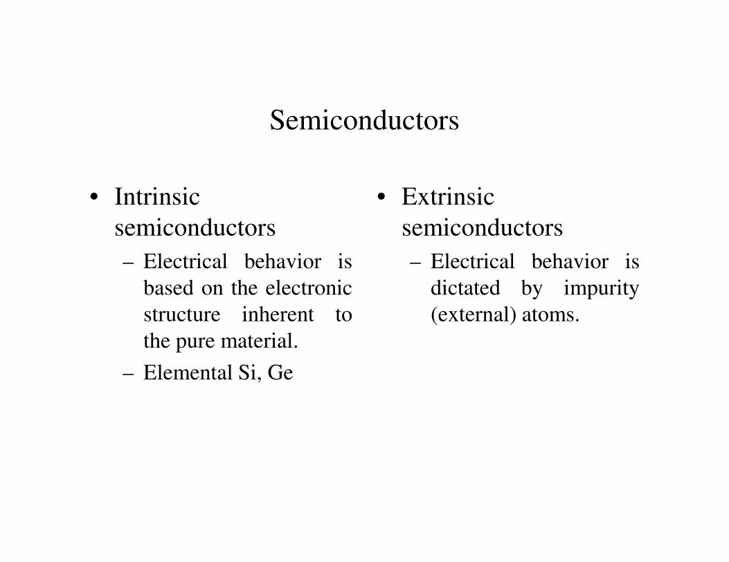
Semiconductors
• Intrinsic
semiconductors
– Electrical behavior is
based on the electronic
• Extrinsic
semiconductors
– Electrical behavior is
dictated by impuritybased on the electronic
structure inherent to
the pure material.
– Elemental Si, Ge
dictated by impurity
(external) atoms.
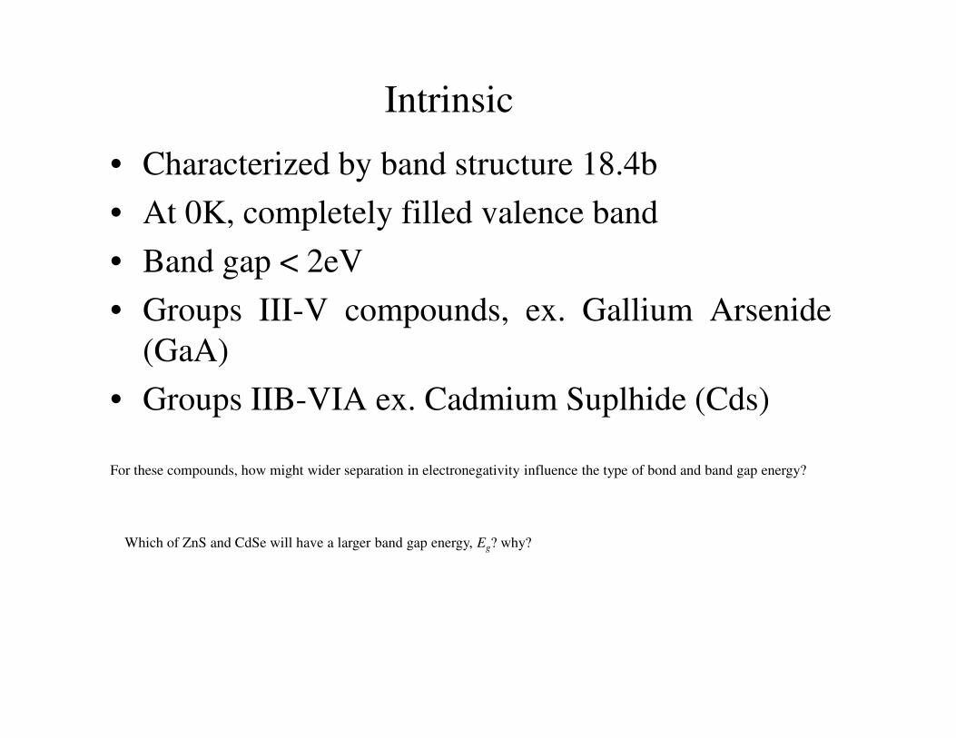
Intrinsic
• Characterized by band structure 18.4b
• At 0K, completely filled valence band
• Band gap < 2eV
• Groups III-V compounds, ex. Gallium Arsenide
(GaA)
• Groups IIB-VIA ex. Cadmium Suplhide (Cds)
For these compounds, how might wider separation in electronegativity influence the type of bond and band gap energy?
Which of ZnS and CdSe will have a larger band gap energy, Eg? why?
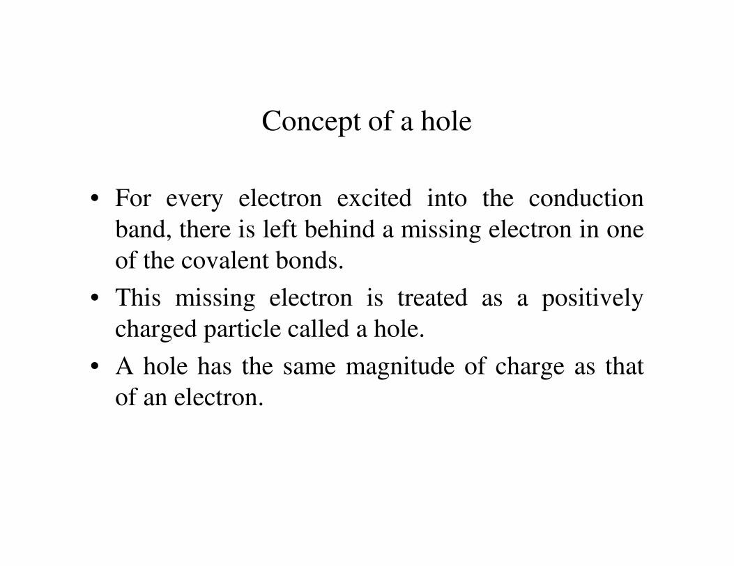
Concept of a hole
• For every electron excited into the conduction
band, there is left behind a missing electron in one
of the covalent bonds.
• This missing electron is treated as a positively• This missing electron is treated as a positively
charged particle called a hole.
• A hole has the same magnitude of charge as that
of an electron.
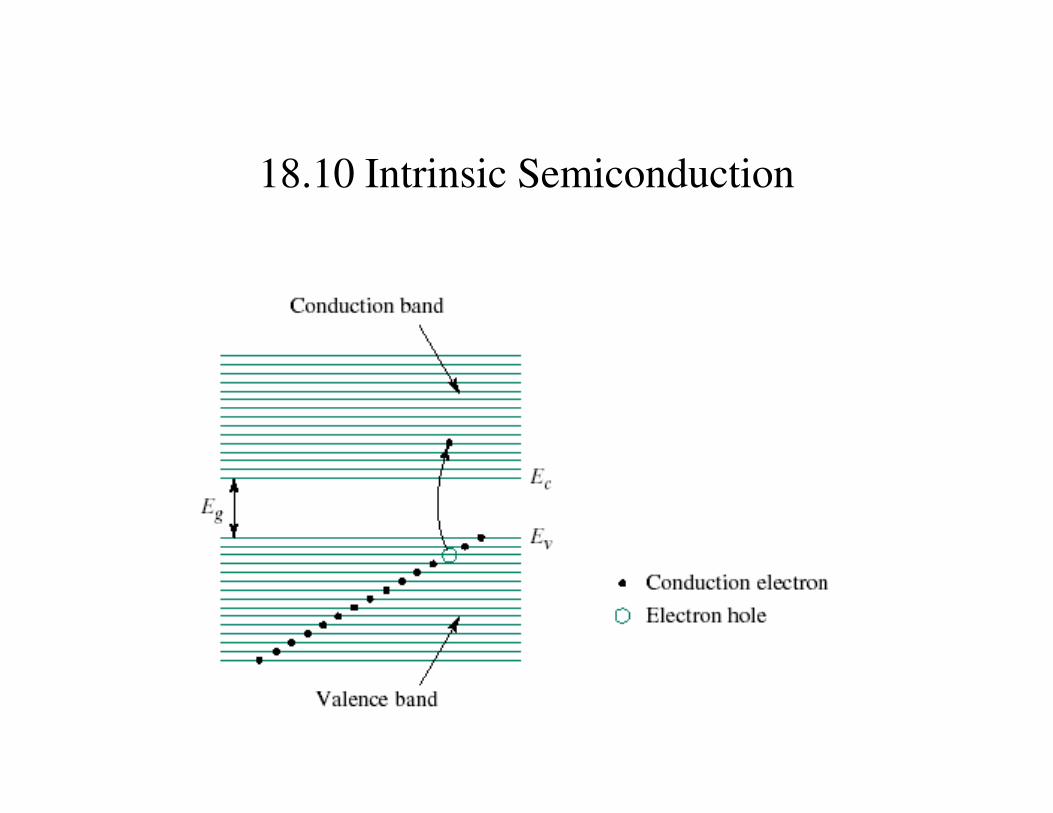
18.10 Intrinsic Semiconduction
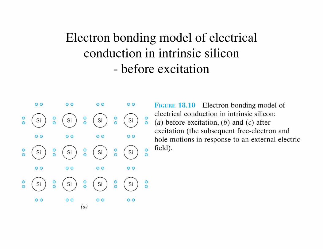
Electron bonding model of electrical
conduction in intrinsic silicon
- before excitation
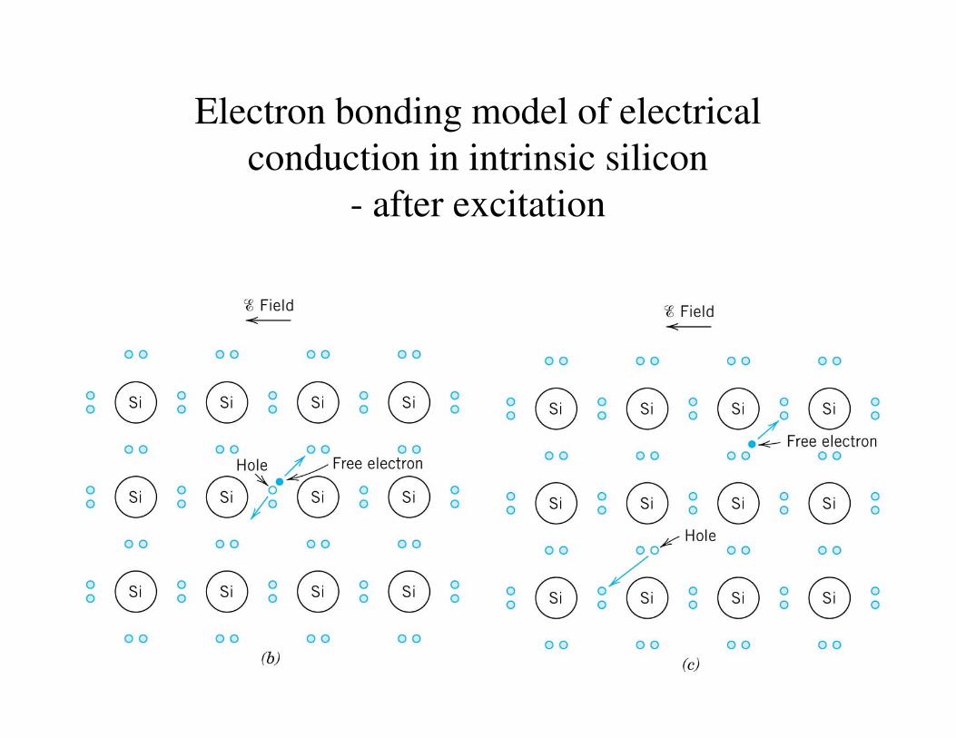
Electron bonding model of electrical
conduction in intrinsic silicon
- after excitation
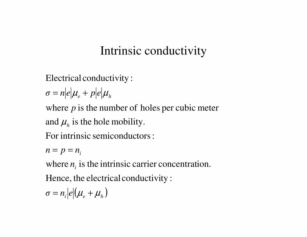
Intrinsic conductivity
he
p
epenσ
µ
µµ +=
mobility. hole theis and
meter cubicper holes ofnumber theis where
:tyconductivi Electrical
( )hei
i
i
h
enσ
n
npn
µµ
µ
+=
==
:tyconductivi electrical theHence,
ion.concentratcarrier intrinsic theis where
:torssemiconduc intrinsicFor
mobility. hole theis and
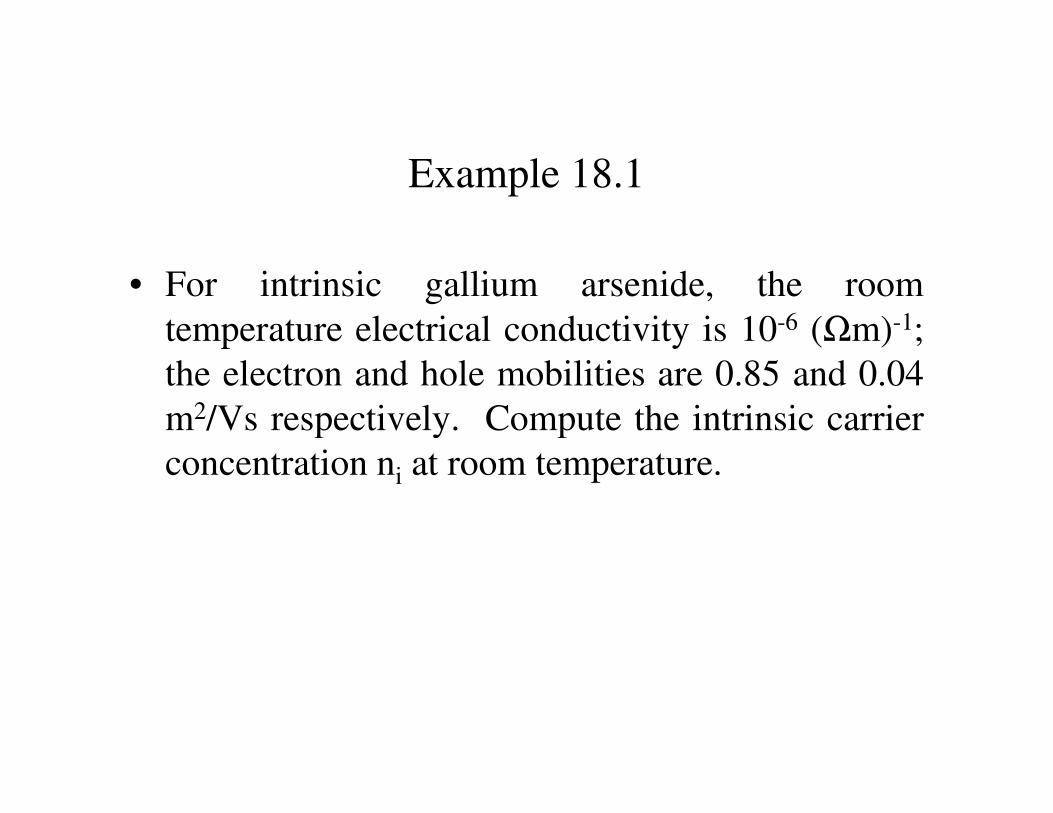
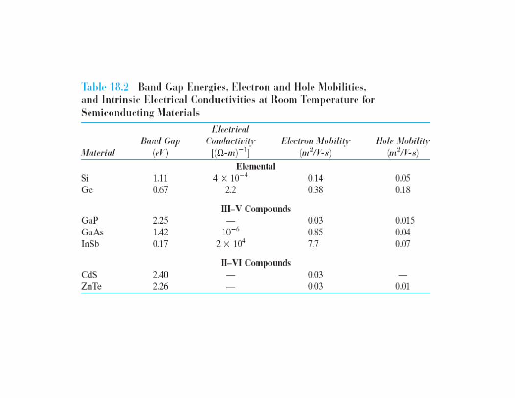
Example 18.1
• For intrinsic gallium arsenide, the room
temperature electrical conductivity is 10-6 (Ωm)-1;
the electron and hole mobilities are 0.85 and 0.04
m2/Vs respectively. Compute the intrinsic carrierm2/Vs respectively. Compute the intrinsic carrier
concentration ni at room temperature.
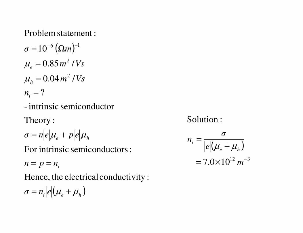
( )
i
h
e
n
Vsm
Vsm
mσ
µ
µ
=
=
=
Ω=−−
:Theory
torsemiconduc intrinsic -
?
/04.0
/85.0
10
:statement Problem
2
2
16
:Solution
( )hei
i
he
enσ
npn
epenσ
µµ
µµ
+=
==
+=
:tyconductivi electrical theHence,
:torssemiconduc intrinsicFor
:Theory
( )312100.7
:Solution
−×=
+=
m
e
σn
he
iµµ
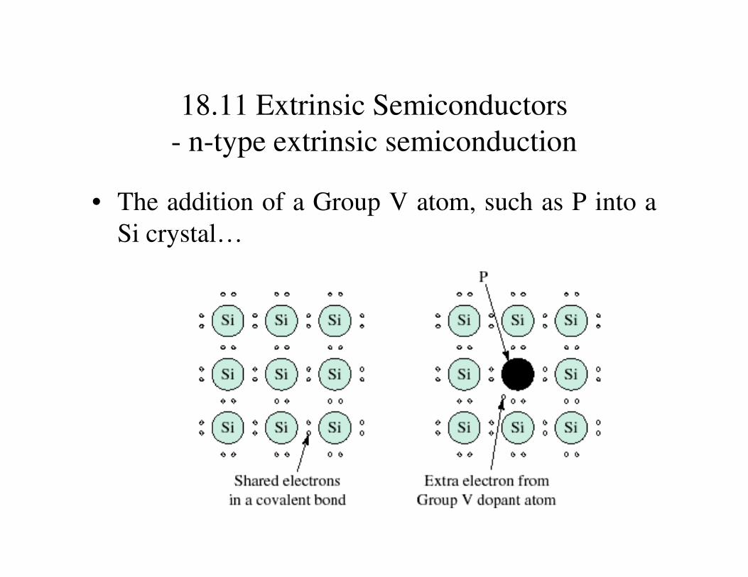
18.11 Extrinsic Semiconductors
- n-type extrinsic semiconduction
• The addition of a Group V atom, such as P into a
Si crystal…
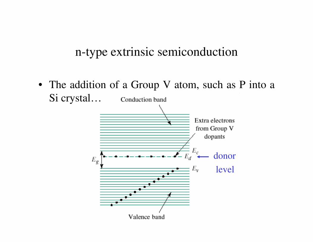
n-type extrinsic semiconduction
• The addition of a Group V atom, such as P into a
Si crystal…
donor
level
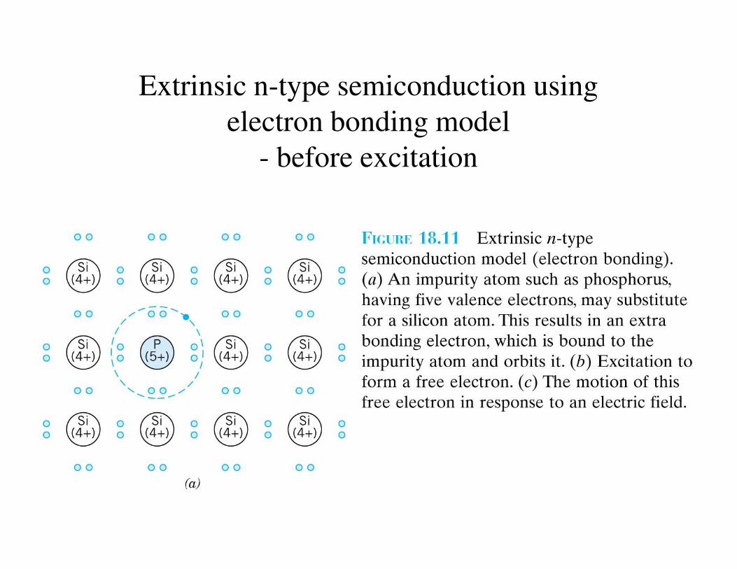
Extrinsic n-type semiconduction using
electron bonding model
- before excitation
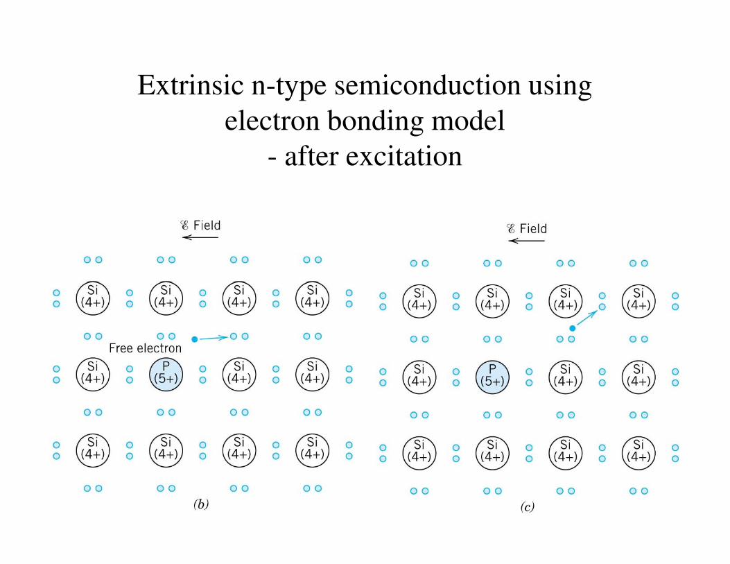
Extrinsic n-type semiconduction using
electron bonding model
- after excitation
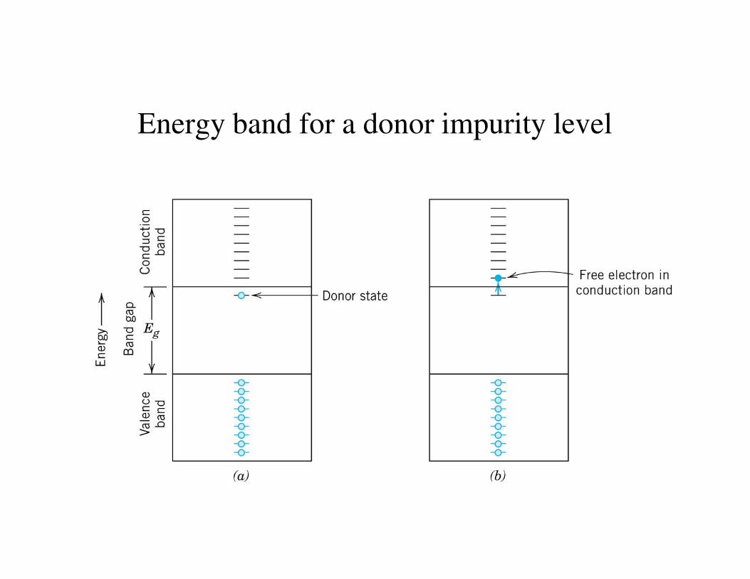
Energy band for a donor impurity level
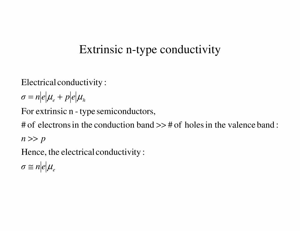
Extrinsic n-type conductivity
he epenσ µµ +=
tors,semiconduc type-n extrinsicFor
:tyconductivi Electrical
eenσ
pn
µ≅
>>
>>
:tyconductivi electrical theHence,
:band valencein the holes of # band conduction in the electrons of #
tors,semiconduc type-n extrinsicFor
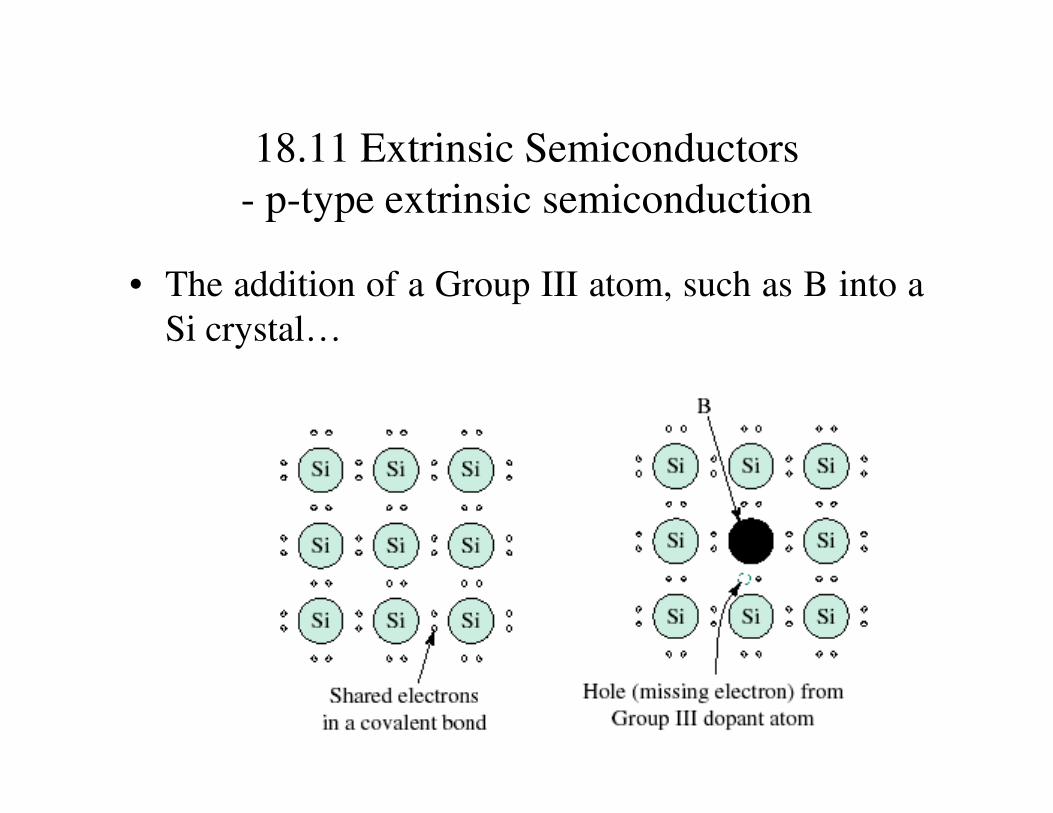
18.11 Extrinsic Semiconductors
- p-type extrinsic semiconduction
• The addition of a Group III atom, such as B into a
Si crystal…
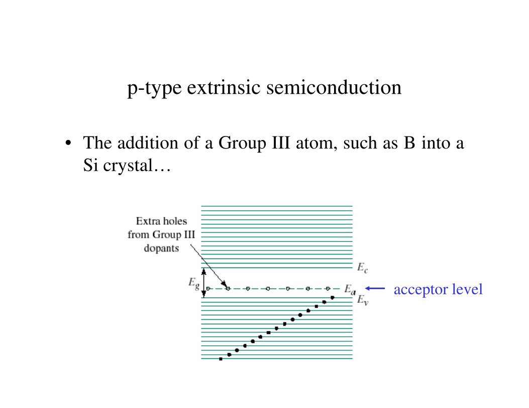
p-type extrinsic semiconduction
• The addition of a Group III atom, such as B into a
Si crystal…
acceptor level
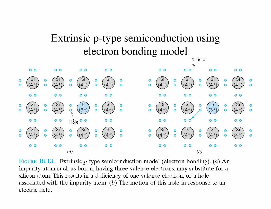
Extrinsic p-type semiconduction using
electron bonding model
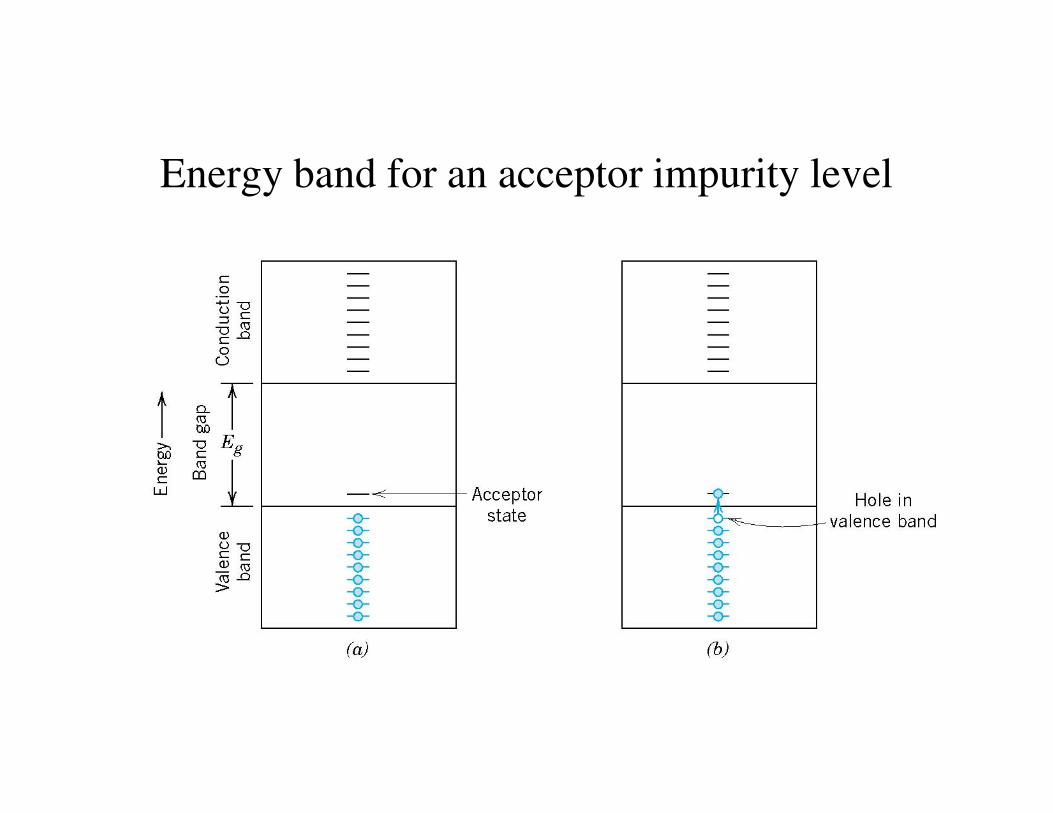
Energy band for an acceptor impurity level

Extrinsic p-type conductivity
he epenσ µµ +=
tors,semiconduc type-p extrinsicFor
:tyconductivi Electrical
hepσ
pn
µ≅
<<
<<
:tyconductivi electrical theHence,
:band valencein the holes of # band conduction in the electrons of #
tors,semiconduc type-p extrinsicFor
Doping
• Extrinsic semiconductors are produced from
materials that are initially extremely pure.
• Controlled concentrations of specific donors or
acceptors are added.acceptors are added.
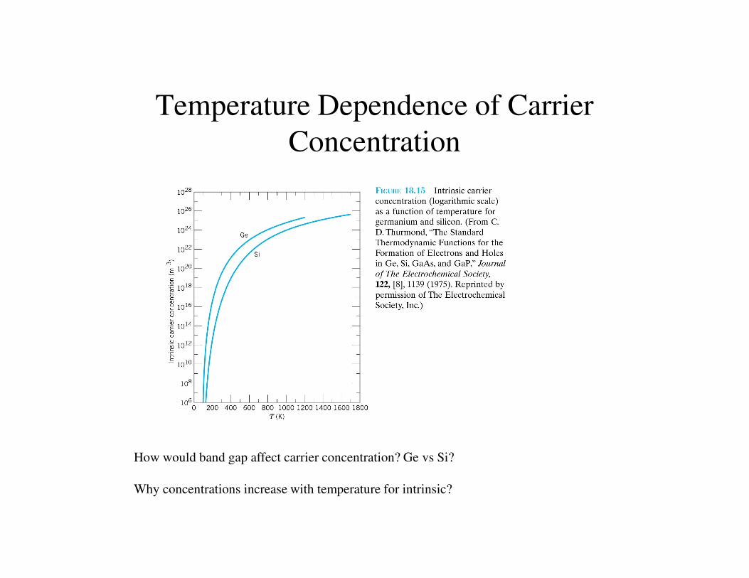
Temperature Dependence of Carrier
Concentration
How would band gap affect carrier concentration? Ge vs Si?
Why concentrations increase with temperature for intrinsic?
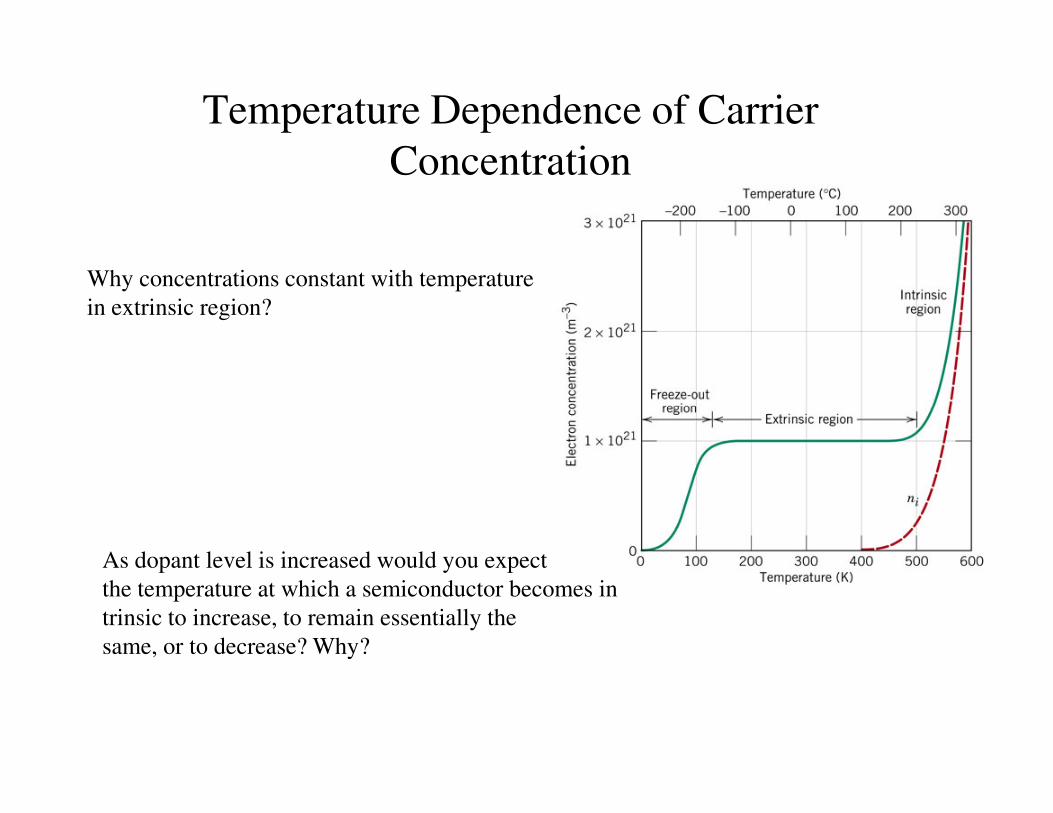
Temperature Dependence of Carrier
Concentration
Why concentrations constant with temperature
in extrinsic region?
As dopant level is increased would you expect
the temperature at which a semiconductor becomes in
trinsic to increase, to remain essentially the
same, or to decrease? Why?
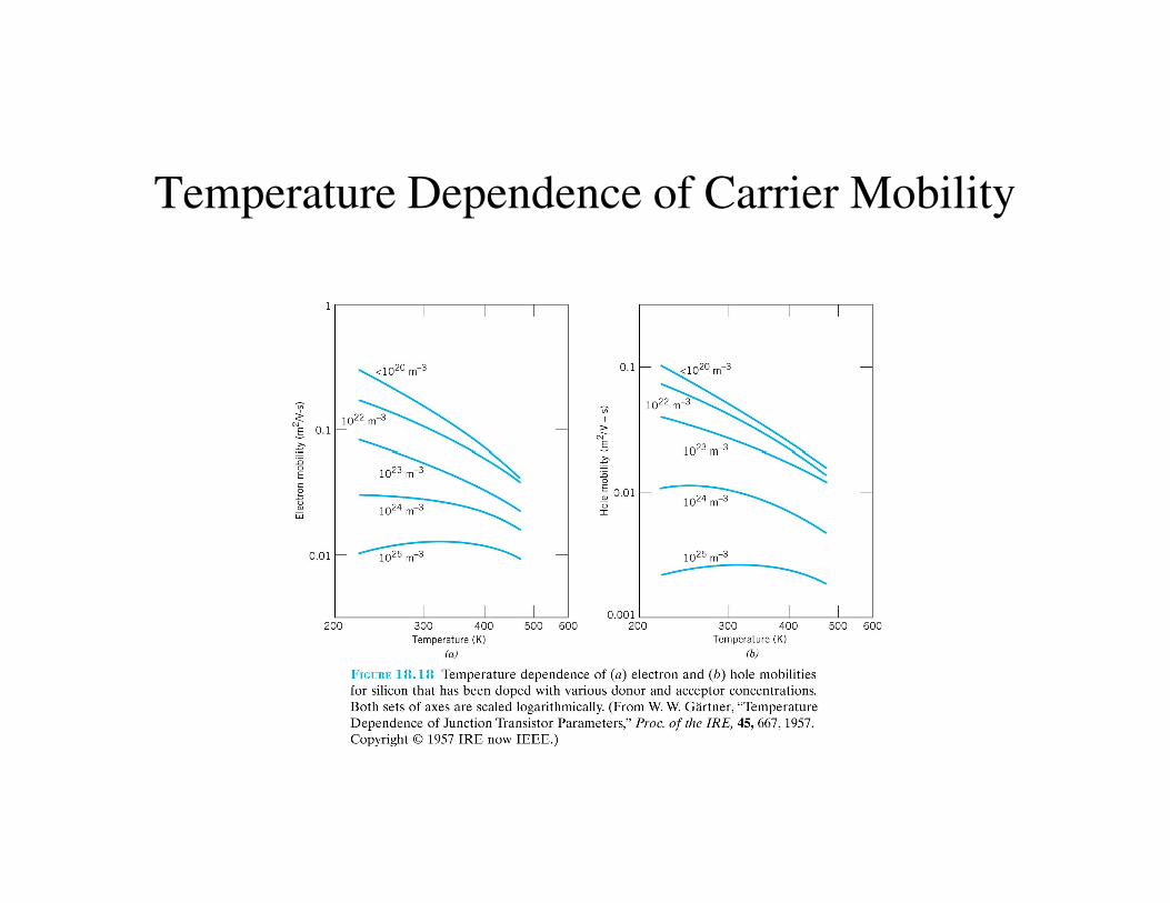
Temperature Dependence of Carrier Mobility
Example 18.2
• Calculate the electrical conductivity of intrinsic
silicon at 423 K.
epenσ
KT
σ
µµ +=
=
=
:Theory
silicon intrinsic -
423
?
:statement Problem
( )hei
i
he
enσ
npn
epenσ
µµ
µµ
+=
==
+=
:tyconductivi electrical theHence,
:torssemiconduc intrinsicFor
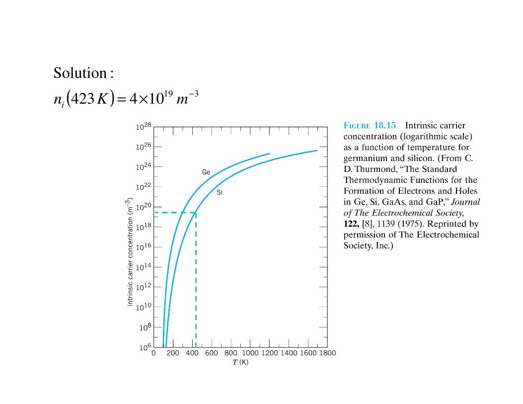
( ) 319104423
:Solution
−×= mKni
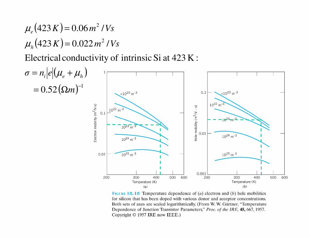
( )
( )
( )
( ) 1
2
2
52.0
:K 423at Si intrinsic ofty conductivi Electrical
/022.0423
/06.0423
−Ω=
+=
=
=
m
enσ
VsmK
VsmK
hei
h
e
µµ
µ
µ
Example 18.3
• To high-purity silicon is added 1023 m-3 arsenic
atoms.
– Is this material n-type or p-type semiconductor?
– Calculate the room temperature electrical conductivity– Calculate the room temperature electrical conductivity
of this material.
– Compute the conductivity at 100 C.
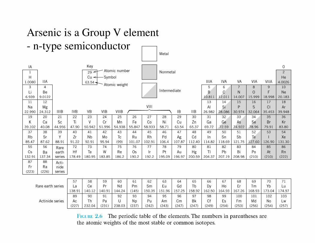
Arsenic is a Group V element
- n-type semiconductor
( )KT
mn
σ
=
=
=−
:Theory
torsemiconduc extrinsic type-n -
re temperaturoom298
10
?
:statement Problem
323
e
he
enσ
pn
epenσ
µ
µµ
≅
>>
+=
:tyconductivi electrical theHence,
:torssemiconduc extrinsic type-nFor
:Theory
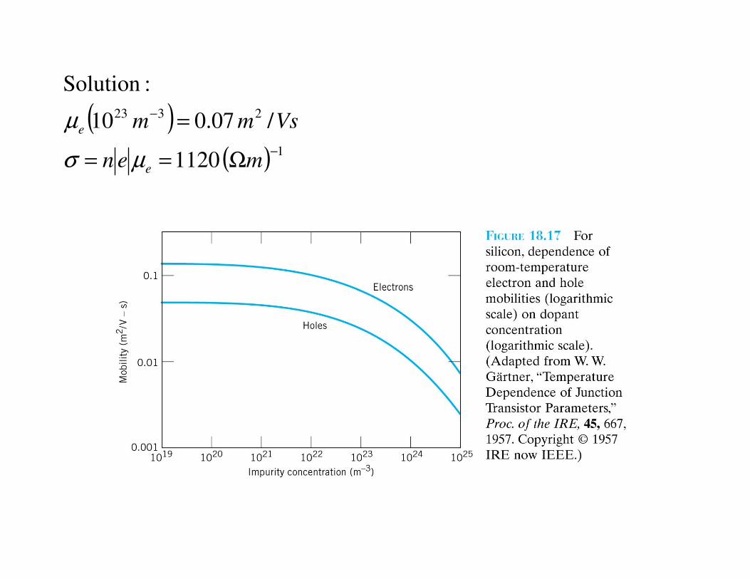
( )( ) 1
2323
1120
/07.010
:Solution
−
−
Ω==
=
men
Vsmm
e
e
µσ
µ
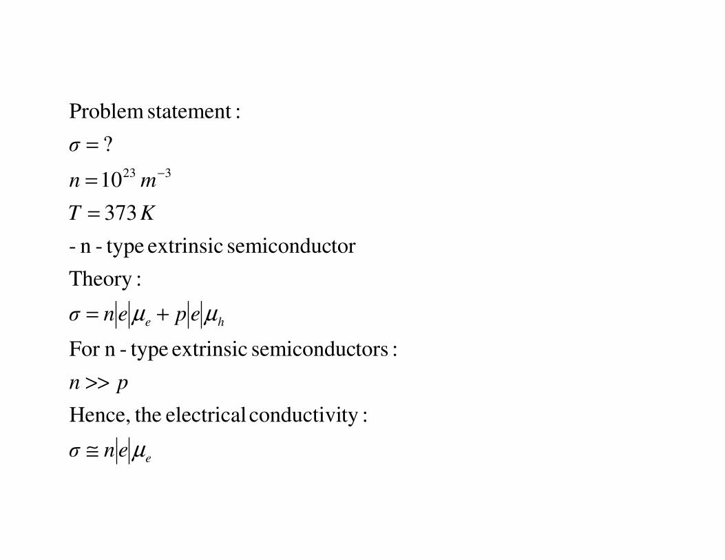
KT
mn
σ
=
=
=−
:Theory
torsemiconduc extrinsic type-n -
373
10
?
:statement Problem
323
e
he
enσ
pn
epenσ
µ
µµ
≅
>>
+=
:tyconductivi electrical theHence,
:torssemiconduc extrinsic type-nFor
:Theory
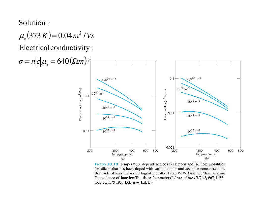
( )
( ) 1
2
640
:tyconductivi Electrical
/04.0373
:Solution
−Ω==
=
menσ
VsmK
e
e
µ
µ


![B ohm’s Theorem for Resource Lambda Calculus through ...manzonetto/papers/mp11.pdf · B ohm’s theorem in the -calculus. B ohm’s theorem [ 1] is a fundamental result in the untyped](https://static.fdocument.org/doc/165x107/5e7e4f9f8906a83c474a9748/b-ohmas-theorem-for-resource-lambda-calculus-through-manzonettopapersmp11pdf.jpg)