FPGA Implementation using VHDL of the AES-GCM 256-bit ...
45
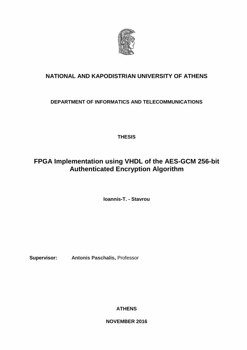
NATIONAL AND KAPODISTRIAN UNIVERSITY OF ATHENS DEPARTMENT OF INFORMATICS AND TELECOMMUNICATIONS THESIS FPGA Implementation using VHDL of the AES-GCM 256-bit Authenticated Encryption Algorithm Ioannis-T. - Stavrou Supervisor: Antonis Paschalis, Professor ATHENS NOVEMBER 2016
Transcript of FPGA Implementation using VHDL of the AES-GCM 256-bit ...
NATIONAL AND KAPODISTRIAN UNIVERSITY OF ATHENS
DEPARTMENT OF INFORMATICS AND TELECOMMUNICATIONS
THESIS
FPGA Implementation using VHDL of the AES-GCM 256-bit Authenticated Encryption Algorithm
Ioannis-T. - Stavrou
Supervisor: Antonis Paschalis, Professor
ATHENS
NOVEMBER 2016
ΕΘΝΙΚΟ ΚΑΙ ΚΑΠΟΔΙΣΤΡΙΑΚΟ ΠΑΝΕΠΙΣΤΗΜΙΟ ΑΘΗΝΩΝ
ΣΧΟΛΗ ΘΕΤΙΚΩΝ ΕΠΙΣΤΗΜΩΝ
ΤΜΗΜΑ ΠΛΗΡΟΦΟΡΙΚΗΣ ΚΑΙ ΤΗΛΕΠΙΚΟΙΝΩΝΙΩΝ
ΠΤΥΧΙΑΚΗ ΕΡΓΑΣΙΑ
Υλοποίηση σε FPGA με τη Χρήση VHDL του Αλγόριθμου Κρυπτογράφησης με Πιστοποίηση Αυθεντικότητας
AES-GCM 256-bit
Ιωάννης - Θ. - Σταύρου
Επιβλέπων: Αντώνης Πασχάλης, Καθηγητής
ΑΘΗΝΑ
ΝΟΕΜΒΡΙΟΣ 2016
THESIS
FPGA Implementation using VHDL of the AES-GCM 256-bit Authenticated Encryption Algorithm
Ioannis - T. - Stavrou
Α.Μ.: 1115200700128
Supervisor: Antonis Paschalis, Professor
ΠΤΥΧΙΑΚΗ ΕΡΓΑΣΙΑ
Υλοποίηση σε FPGA με τη Χρήση VHDL του Αλγόριθμου Κρυπτογράφησης με Πιστοποίηση Αυθεντικότητας AES-GCM 256-bit
Ιωάννης - Θ. - Σταύρου
Α.Μ.:1115200700128
Επιβλέπων: Αντώνης Πασχάλης, Καθηγητής
ABSTRACT
Achieving high-speed network performance along with data integrity and security was always a challenge. The necessity to communicate through public channels securely led to the use of asymmetric key cryptography algorithms that commonly use a “hand-shake” mechanism allowing the implementation of a “trust” system that could quarantine the security of the transaction and the integrity of the data as long as the algorithm could provide strong resistance to cryptographic attacks. Although, there is no mathematical proof that these algorithms are invulnerable to attacks there is strong indication that they are highly resistant to most of them, making brute force the only attack that can have a 100% success rate which is countered by the huge computational power someone needs to succeed.
While asymmetric key cryptography algorithms where the solution to public communication, the ongoing demand for higher bandwidth made the use of them inefficient, because the complexity of the algorithms demanded a processing cost that were creating latency gaps. A solution to this problem was the use of symmetric key algorithms for data transactions were the processing cost is much lower, so that the transaction security was intact but the bottleneck on the encryption/decryption speed limit was increased.
The analysis in symmetric cryptographic algorithms resulted in the creation of the Advanced Encryption Standard (AES) published by NIST in 2001. Also the need of authentication and integrity of information transmitted, resulted in the creation of the
AES-GCM mode which can authenticate a stream of data (up to 68𝐺𝑏) with reliable and efficient way. Both algorithms have the advantage to be easily implemented in both software and hardware. With the demand of high speed interaction between networks and systems, it became clear that hardware solutions were the leading option to cover this demand. FPGA-based IP cores can implement those algorithms, with the use of hardware description language like VHDL, and provide accurate, reliable and high speed data process.
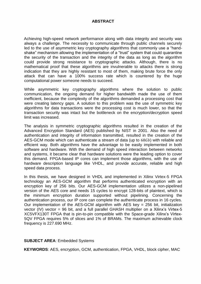
In this thesis, we have designed in VHDL and implemented in Xilinx Virtex-5 FPGA technology an AES-GCM algorithm that performs authenticated encryption with an encryption key of 256 bits. Our AES-GCM implementation utilizes a non-pipelined version of the AES core and needs 15 cycles to encrypt 128-bits of plaintext, which is the minimum encryption duration supported without pipelining. Concerning the authentication process, our IP core can complete the authenticate process in 16 cycles. Our implementation of the AES-GCM algorithm with AES key = 256 bit, initialization vector (IV) vector = 96 bit, and a full parallel GHASH multiplier on a Xilinx’s Virtex-5 XC5VFX130T FPGA that is pin-to-pin compatible with the Space-grade Xilinx’s Virtex-5QV FPGA requires 5% of slices and 1% of BRAMs. The maximum achievable clock frequency is 227.690 MHz.
SUBJECT AREA: Embedded Systems
KEYWORDS: AES, encryption, GCM, authentication, FPGA, VHDL, block cipher, MAC
ΠΕΡΙΛΗΨΗ
Η επίτευξη υψηλών ταχυτήτων μετάδοσης δεδομένων στα τηλεπικοινωνιακά δίκτυα μαζί με την ανάγκη για αξιόπιστη και ασφαλή μετάδοση των πληροφοριών ήταν πάντα μια πρόκληση. Η ανάγκη για επικοινωνία μέσο δημόσιων δικτύων με ασφαλή τρόπο, οδήγησε στην χρήση αλγόριθμων κρυπτογράφηση ασύμμετρου κλειδιού, οπού ένας μηχανισμός «χειραψίας» εξασφαλίζει την ασφαλή μετάδοση δεδομένων και την ακεραιότητα αυτών. Παρόλο που μαθηματικά δεν έχει αποδειχτεί ότι αυτοί οι αλγόριθμοι είναι άτρωτοι σε κρυπτογραφικές επιθέσεις, υπάρχουν ισχυρές ενδείξεις ότι είναι ανθεκτικοί στις περισσότερες κάνοντας την επίθεση ωμής βίας (bruteforce) την μόνη που έχει 100% πιθανότητα επιτυχίας δεδομένης τεράστιας υπολογιστικής ισχύος.
Ενώ οι αλγόριθμοι ασύμμετρου κλειδιού ήταν η λύση για τις δημόσιες επικοινωνίες, η συνεχής απαίτηση για μεγαλύτερο εύρος ζώνης, έκανε την χρήση τους μη αποδοτική λόγο του υψηλού κόστους που απαιτούν σε υπολογιστική ισχύ. Η λύση στο πρόβλημα ήρθε με την υβριδική χρήση αλγορίθμων συμμετρικού και ασύμμετρου κλειδιού, έτσι ώστε να διατηρείτε ασφαλή μεταφορά δεδομένων αλλά η ταχύτητα επεξεργασίας των δεδομένων να αυξηθεί σημαντικά.
Η ανάλυση στους συμμετρικούς αλγόριθμους οδήγησε στην δημιουργία του αλγορίθμου κρυπτογράφησης Advanced Encryption Standard (AES) που δημοσιεύτηκε από τον οργανισμό NIST το 2001, ως διάδοχο του DES. Η ανάγκη για αυθεντικοποίηση των δεδομένων οδήγησε στην δημιουργίας του αλγορίθμου GCM όπου μπορεί να αυθεντικοποιήσει μια ροή δεδομένων με αξιόπιστο και αποδοτικό τρόπο. Και οι δύο αλγόριθμοι έχουν το πλεονέκτημα ότι μπορεί να υλοποιηθούν εύκολα τόσο σε λογισμικό όσο και σε υλικό. Με την ζήτηση για υψηλές ταχύτητες να είναι μεγάλη, η υλοποίηση σε υλικό γίνεται μια όλο και πιο ελκυστική επιλογή. Οι πυρήνες IP με βάση την τεχνολογία FPGA μπορούν να υλοποιήσουν αυτούς τους αλγόριθμους με την χρήση γλωσσών περιγραφής υλικού όπως η VHDL,και να προσφέρουν αξιόπιστη και υψηλών ταχυτήτων επεξεργασία δεδομένων.
Σε αυτή την εργασία σχεδιάσαμε χρησιμοποιώντας την γλώσσα VHDL και υλοποιήσαμε στο FPGA Virtex 5 XC5VFX130T της Xilinx, τον αλγόριθμό κρυπτογράφησης AES με το πρωτόκολλο αυθεντικοποίησης GCM, με μέγεθος κλειδιού στα 256 bits. Η υλοποίηση μας βασίζεται σε μια μη σωληνομένη εκδοχή του αλγορίθμου AES που μπορεί να κρυπτογραφήσει ένα μπλοκ 128 bits σε 15 κύκλους. Η αυθεντικοποίηση του μηνύματος μπορεί να επιτευχθεί σε 16 κύκλους. Η υλοποίηση μας με IV = 96 bits και παράλληλο πολλαπλασιαστή χρειάζεται 5% από τα slices και 1% από τα BRAMs του Virtex-5 XC5VFX130T FPGA. Η μέγιστη δυνατή συχνότητα είναι 227.690 MHz.
ΘΕΜΑΤΙΚΗ ΠΕΡΙΟΧΗ: Ενσωματωμένα Συστήματα
ΛΕΞΕΙΣ ΚΛΕΙΔΙΑ: AES, κρυπτογράφηση, GCM, αυθεντικοποίηση, VHDL, FPGA, μπλοκ κρυπτογράμματος, MAC

ACKNOWLEDGEMENT
I would like to thank my professor Antonis Paschalis for entrusting me with this thesis and providing me with the intellectual tools necessary to bring this project to fruition. Also, I would like thank the post doctorate researcher, Dr. Georgios Theodorou for guiding me through the steps of this thesis and bearing with me till the end.
CONTENTS
1. INTRODUCTION .................................................................................................... 11
2. CRYPTOGRAPHY ................................................................................................. 12
2.1 AES - (Advanced Encryption Standard) ........................................................................................ 12
2.2 GCM - (The Galois/Counter Mode) ............................................................................................... 13
3. MATHEMATICAL COMPONENTS OF AES-GCM ................................................ 15
3.1 Basic functions .............................................................................................................................. 15
3.2 AES functions ................................................................................................................................ 16
3.3 GCM functions ............................................................................................................................... 20
4. DESIGN OF AES-GCM-256 ................................................................................... 22
4.1 AES Module ................................................................................................................................... 22 4.1.1 Key Scheduler Module .............................................................................................................. 22 4.1.2 Control Unit ............................................................................................................................... 23
4.2 GCM Module ................................................................................................................................. 24 4.2.1 GF multiplier .............................................................................................................................. 26 4.2.2 GHASH ...................................................................................................................................... 28 4.2.3 GCTR ........................................................................................................................................ 29
5. IMPLEMENTATION AND SIMULATION ............................................................... 31
5.1 AES-256 ........................................................................................................................................ 31
5.2 GF Multiplier .................................................................................................................................. 33
5.3 GCM .............................................................................................................................................. 34 5.3.1 GCM control unit ....................................................................................................................... 35 5.3.2 AES-GCM module ..................................................................................................................... 37
5.4 Validation ....................................................................................................................................... 41 5.4.1 Test case 1 ................................................................................................................................ 41 5.4.2 Test case 2 ................................................................................................................................ 42 5.4.3 Test case 3 ................................................................................................................................ 43
REFERENCES .............................................................................................................. 45
FIGURE TABLE
Figure 1: AES number of rounds ................................................................................... 16
Figure 2: State array 128-bit .......................................................................................... 17
Figure 3: AES S-box ...................................................................................................... 18
Figure 4: ShiftRows illustration ...................................................................................... 18
Figure 5: MixColumns illustration 1 ................................................................................ 19
Figure 6: MixColumns illustration 2 ................................................................................ 19
Figure 7: Rcon rounds ................................................................................................... 22
Figure 8: AES control FSM ............................................................................................ 23
Figure 9: AES-GCM algorithm ....................................................................................... 25
Figure 10: AES-GCM algorithm for 2 cipher blocks and 1 for ADD ............................... 25
Figure 11: Matrovito multiplier logic gate representation ............................................... 27
Figure 12: Matrovito model ............................................................................................ 28
Figure 13: GHASH illustration ........................................................................................ 29
Figure 14: GCTR illustration .......................................................................................... 30
Figure 15: AES schematic ............................................................................................. 32
Figure 16: AES test bench ............................................................................................. 33
Figure 17: Mastrovito multiplier test bench .................................................................... 34
Figure 18: Life cycle of data ........................................................................................... 35
Figure 19: GCM control FSM ......................................................................................... 36
Figure 20: Test bench of the GCM control unit .............................................................. 37
Figure 21: GCM schematic ............................................................................................ 37
Figure 22: GCM test bench............................................................................................ 38
Figure 23: TAG test bench result ................................................................................... 39
Figure 24: Test case 1 results ....................................................................................... 41
Figure 25: Test case 2 results ....................................................................................... 43
Figure 26: Test case 3 results ....................................................................................... 44
LIST OF TABLES
Table 1 Mastrovito multiplier utilization .......................................................................... 33
Table 2: Hardware specs ............................................................................................... 39
Table 3: Timing and memory report ............................................................................... 40
Table 4: Total utilization ................................................................................................. 40
Table 5: Test vector 1 .................................................................................................... 41
Table 6: Test vector 2 .................................................................................................... 42
Table 7: Test vector 3 .................................................................................................... 44
FPGA Implementation using VHDL of AES-GCM 256-bit encryption core
I.Stavrou 11
1. INTRODUCTION
Embedded systems are a common solution to cryptographic algorithms for network communication uses. They can provide high bandwidth, maximizing throughput and reliability. The rising trend on embedded systems is the FPGA. Field Programmable Gate Arrays (FPGAs) are semiconductor devices based around a matrix of configurable logic blocks (CLBs) connected via programmable interconnects. FPGAs are reconfigurable devices that can implement any desired application or functionality requirements after manufacturing. This feature distinguishes FPGAs from Application Specific Integrated Circuits (ASICs), which are custom manufactured for specific design tasks. While FPGA are inferior to ASIC in matter of processing power, low cost and design flexibility make FPGA a fitting solution to certain applications like network communications and aerospace applications.
With data encryption, the need for authentication required the use of specific operation modes that made the computational processes more demanding. The need for minimum latency led to the creation of algorithms that could be parallel processed and implemented in both software and hardware. The Galois/Counter Mode is an authentication mode used along with the AES algorithm as an expansion. Meeting the required criteria, GCM is an efficient authentication algorithm that can be parallelized, making its computational cycle needs in a range of 128 cycles to 1 cycle, with cost on chipset area coverage.
In this thesis, we are going to implement the encryption part of a symmetric key cryptographic algorithm, the AES, along with the authentication mode GCM, using VHDL. The system will be implemented in an FPGA device, with main objective the maximum throughput possible which translates to minimum clock cycles needed for completion of operation. With these goals in mind we are going to analyze the core functions of the algorithm, following by performance analysis and hardware limitations.
In Chapter 2 we are going to discuss the background theory necessary to understand how AES-GCM works. In chapter 2.1 we present a reference to the AES and in chapter 2.2 a reference to GCM. Chapter 3 refers to the mathematical components of the algorithms, were in chapter 3.1 we present some basic mathematic notations that we are going to use during our analysis and implementation, in 3.2 we present the AES components and in 3.3 the GCM components. In chapter 4 we make a performance analysis and we structure the basic design that we are going to use in chapter 5 were we implement and simulate the design in a FPGA.
The software we used for this thesis was:
Xilinx ISE 14. 7 WebPack edition for implementation of the code in VHDL
Xilinx Isim for test bench simulation and validation
The hardware we used to use for this thesis was:
Virtex 5 XC5VLX50T with package FF1136 of Xilinx FPGA family.
FPGA Implementation using VHDL of AES-GCM 256-bit encryption core
I.Stavrou 12
2. CRYPTOGRAPHY
In this chapter we are going to present the theoretical background that is required to understand the key points of the encryption and authentication mechanism of AES-GCM. In chapter 2.1 we discuss the AES algorithm in a simplified manner so that we can understand the importance of the algorithm and why is one of the most powerful symmetric key cryptographic algorithms. In chapter 2.2 we analyze the authentication modes that were proposed from NIST and why GCM is our choice of authentication.
2.1 AES - (Advanced Encryption Standard)
AES is a symmetric block cipher algorithm used to protect classified information from being compromised by a not authorized user. The encryption mechanism allows only those that have access to the key used for the encryption to have access to the information. Also known as Rijndael cipher algorithm, AES was proposed by two Belgian cryptographers, Joan Daemen and Vincent Rijmen, who submitted it to NIST during the AES selection process. The need of increased security, flexibility in implementation and high performance led Rijndael to be the winning candidate of the competition, making it a security standard by NIST, replacing 3DES and becoming the recommended option for sensitive data transactions.
The basic criteria AES needed to meet were:
It can handle 128-bit data size blocks.
Accepts key size blocks of 128, 192 and 256 bits.
Has no academic weakness worse than exhaustive key search.
It should be as fast as 3DES.
The criteria were met and the standard was established by NIST in 2001.
AES encryption mechanism, as all block cipher algorithms, consists of a key and data for encryption. The data are separated in a number of static size blocks with upper ceiling logic, and then each block is encrypted to what is known as cipher block. Then the cipher information can only be decrypted by the same key use for encryption synthesizing each block to the original data. Both in encryption and decryption the number of operations is the same but the operations are reversed. While the key block size is unlimited, the data block size can be a maximum of 256 bits. For purposes of performance and optimization the most common values for the key block size are 128, 192 and 256 bits, and a fixed value for the data block size of 128 bits. AES design is based on a substitution-permutation network (SPN), combination of substitution and permutation operations on the block of data and the key given.
The resistance of AES towards differential and linear cryptanalysis comes from an “avalanche effect” created during the algorithm operations, meaning that a bit flip quickly propagates to the complete internal state. This effect is granted by a number of operations which is applied to both data and the key in repetitive process that is called “rounds”. At each round the algorithm uses 4 key operations which scramble the data and prepare it as input for the next round creating a chaining process. In every round,
FPGA Implementation using VHDL of AES-GCM 256-bit encryption core
I.Stavrou 13
with the exception of the final round, these operations apply on a fixed 128-bit block and the key given after it has been expanded. Those operations are: SubBytes, ShiftRows, MixColumns, and AddRoundKey.
The key expansion is a basic operation that expands the initial key input into separate round keys. Each round key is the one that is used at each round making it different from the others. This operation is the one that dictates how many rounds each data block will be processed before becoming the output, according with the key block size given.
The algorithm describing AES with 128-bit data block size given by FIPS is the following:
Cipher (byte in [4*Nb], byte out[4*Nb], word w[Nb*(Nr+1)]) begin Bytestate [4,Nb]
state = in AddRoundKey (state, w[0, Nb-1]) for round = 1 step 1 to Nr–1 SubBytes(state) ShiftRows(state)
MixColumns(state) AddRoundKey(state, w[round*Nb, (round+1)*Nb-1])
end for SubBytes(state) ShiftRows(state) AddRoundKey(state, w[Nr*Nb, (Nr+1)*Nb-1])
out = state end
Where Nbits the number of words (4 bytes) the block has. This number is defined as 4
because we need 4 *4 bytes = 32 bits * 4 to have a 128-bit block. Nr is the number of rounds. The functions describing the algorithm we be presented in chapter 3.1
2.2 GCM - (The Galois/Counter Mode)
An authentication algorithm must quarantine that the data send are authentic and that their source is a user who has access to the encryption key. From 2001 till now, NIST has published a total of 4 recommendations for the block cipher mode of operations SP800-38A, SP800-38B, SP800-38C and SP800-38D.
In SP800-38A there are 5 modes of operation recommended from NIST
Electronic Codebook (ECB) mode
Cipher Block Chaining (CBC) mode,
CipherFeedback (CFB) mode,
Output Feedback (OFB) mode, and
Counter (CTR) mode
FPGA Implementation using VHDL of AES-GCM 256-bit encryption core
I.Stavrou 14
ECB and CTR are non-feedback modes, while CBC, CFB and OFB are feedback modes. Feedback mode means that the result of the current executing step of the algorithm is depended from the previous step. Feedback operations need iterative architecture meaning low performance purposes. For that reason, ECB and CTR are preferred.
In SP800-38B NIST suggested a message authentication code (MAC) based on the cipher block. This cipher-based MAC is called CMAC or Cipher Block Chaining MAC
(CBC-MAC).In SP800-38C NIST introduced a mode of operation called CCM based on symmetric key block cipher where block size is 128 bits. CCM provides the confidentiality and authenticity needed by combining CTR mode and CBC-MAC.
The throughput given by CTR mode is greater than that of CBC-MAC, because in the case of CTR the implementation can be done with pipeline techniques. CBC-MAC implementation cannot be parallelized. Until this point there was no efficient solution for high speed networking.
The fourth and last article covers that gap. In SP800-38D NIST the Galois/Counter Mode of Operation (GCM) is provided with minimum latency and minimum operation overhead as key advantages. This can be achieved because the algorithm can be parallelized, making the multiplication process, which is the most demanding, completed in one single clock circle. One core advantage is that the system is "online" meaning that while you need the length of the message as information for the authentication, this is calculated during the processing of data. Also the initialization vector and all others no-authenticated components can be initialized. GCM provides a strong authentication algorithm which transcends a no-cryptographic check sum or an error detection system.
The GCM authentication mechanism consists of a hashing function, also known as GHASH, where the data to be encrypted and all the additional authentication data are used to create a unique 128-bit block of data known as “tag”. The tag is send along with the encrypted data, and then is used to ensure that the encrypted data belong to someone who has access to the key. A wrong tag will result in a fail indication from the system meaning that the data or a part of them are not authentic.
FPGA Implementation using VHDL of AES-GCM 256-bit encryption core
I.Stavrou 15
3. MATHEMATICAL COMPONENTS OF AES-GCM
In this chapter we are going to describe the mathematical components that we are going to use in our implementation, as long as the notation referring to them. In chapter 3.1 we present some basic function that are needed for our system. In chapter 3.2 we present the core functions of AES and the steps that are necessary for each operation. In chapter 3.3 we analyze the key components of GCM and the additional steps needed.
3.1 Basic functions
The following symbols are the mathematical and operational components we going to need to described the main operation of both AES and GCM algorithms.
Ceiling function - [𝑥] : Returns the smallest integer number which is not
smaller than 𝑥.
Example: [4.7] = 5
Concatenation - || : is the operation in which two bit string are combined
as one.
Example: 0001 ||1001 = 00011001
Special power notation - 0𝑠 : Refers to a bit string with 𝑠 zeros (0).
Example: 07 = 0000000
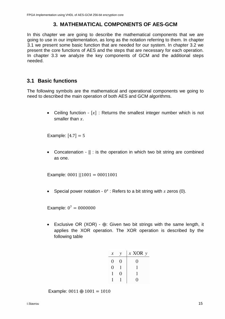
Exclusive OR (XOR) - ⨁: Given two bit strings with the same length, it
applies the XOR operation. The XOR operation is described by the
following table
Example: 0011 ⨁ 1001 = 1010
FPGA Implementation using VHDL of AES-GCM 256-bit encryption core
I.Stavrou 16
Length function - 𝑙𝑒𝑛(𝑥): Returns the length in decimal, of a bit string.
Example: (001) = 3 , 𝑙𝑒𝑛(001||03) = 6
Least/Most significant bits - 𝐿𝑆𝐵𝑠(𝑥), 𝑀𝑆𝐵𝑠(𝑥): Given a bit string 𝑥 and an
integer 𝑠with 𝑠 ≤ 𝑙𝑒𝑛(𝑥), both functions return 𝑠 bits from 𝑥 with 𝑀𝑆𝐵𝑠(𝑥)
returning leftmost bits and 𝐿𝑆𝐵𝑠(𝑥) rightmost bits.
Example: 𝐿𝑆𝐵5(0001001110011) = 10011 , 𝑀𝑆𝐵4(0001001110011) = 0001
Shift operation - 𝑥 ≫ 𝑠, 𝑥 ≪ 𝑠: Given a bit string 𝑥 and an integer 𝑠 it shifts
𝑠 bits from 𝑥 to right (≫) or left (≪). Those operations do not apply on
signed or negative numbers.
Example: 0001100110111 ≫ 4 = 0000000110011 , 101011 ≪ 2 = 101100
3.2 AES functions
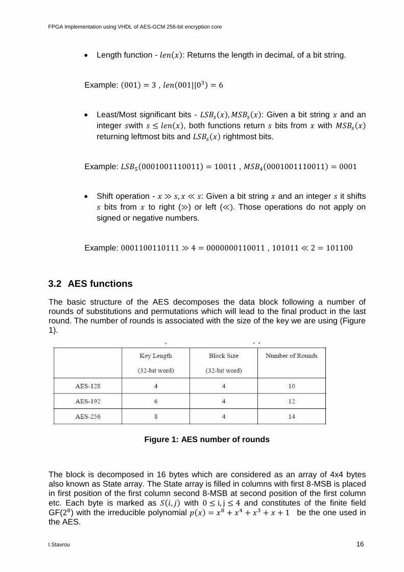
The basic structure of the AES decomposes the data block following a number of rounds of substitutions and permutations which will lead to the final product in the last round. The number of rounds is associated with the size of the key we are using (Figure 1).
Figure 1: AES number of rounds
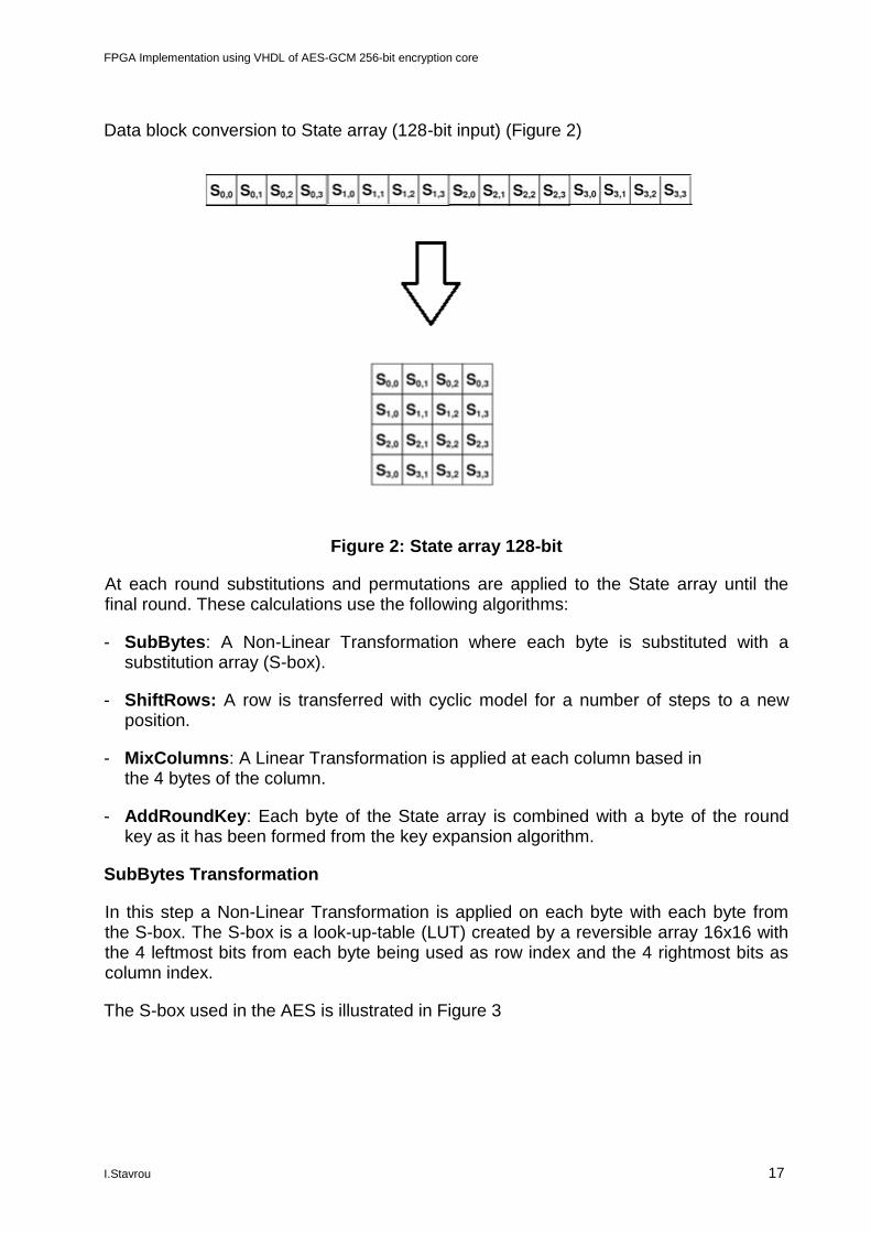
The block is decomposed in 16 bytes which are considered as an array of 4x4 bytes also known as State array. The State array is filled in columns with first 8-MSB is placed in first position of the first column second 8-MSB at second position of the first column
etc. Each byte is marked as 𝑆(𝑖, 𝑗) with 0 ≤ i, j ≤ 4 and constitutes of the finite field
GF(28) with the irreducible polynomial 𝑝(𝑥) = 𝑥8 + 𝑥4 + 𝑥3 + 𝑥 + 1 be the one used in the AES.
FPGA Implementation using VHDL of AES-GCM 256-bit encryption core
I.Stavrou 17
Data block conversion to State array (128-bit input) (Figure 2)
Figure 2: State array 128-bit
At each round substitutions and permutations are applied to the State array until the final round. These calculations use the following algorithms:
- SubBytes: A Non-Linear Transformation where each byte is substituted with a substitution array (S-box).
- ShiftRows: A row is transferred with cyclic model for a number of steps to a new position.
- MixColumns: A Linear Transformation is applied at each column based in the 4 bytes of the column.
- AddRoundKey: Each byte of the State array is combined with a byte of the round key as it has been formed from the key expansion algorithm.
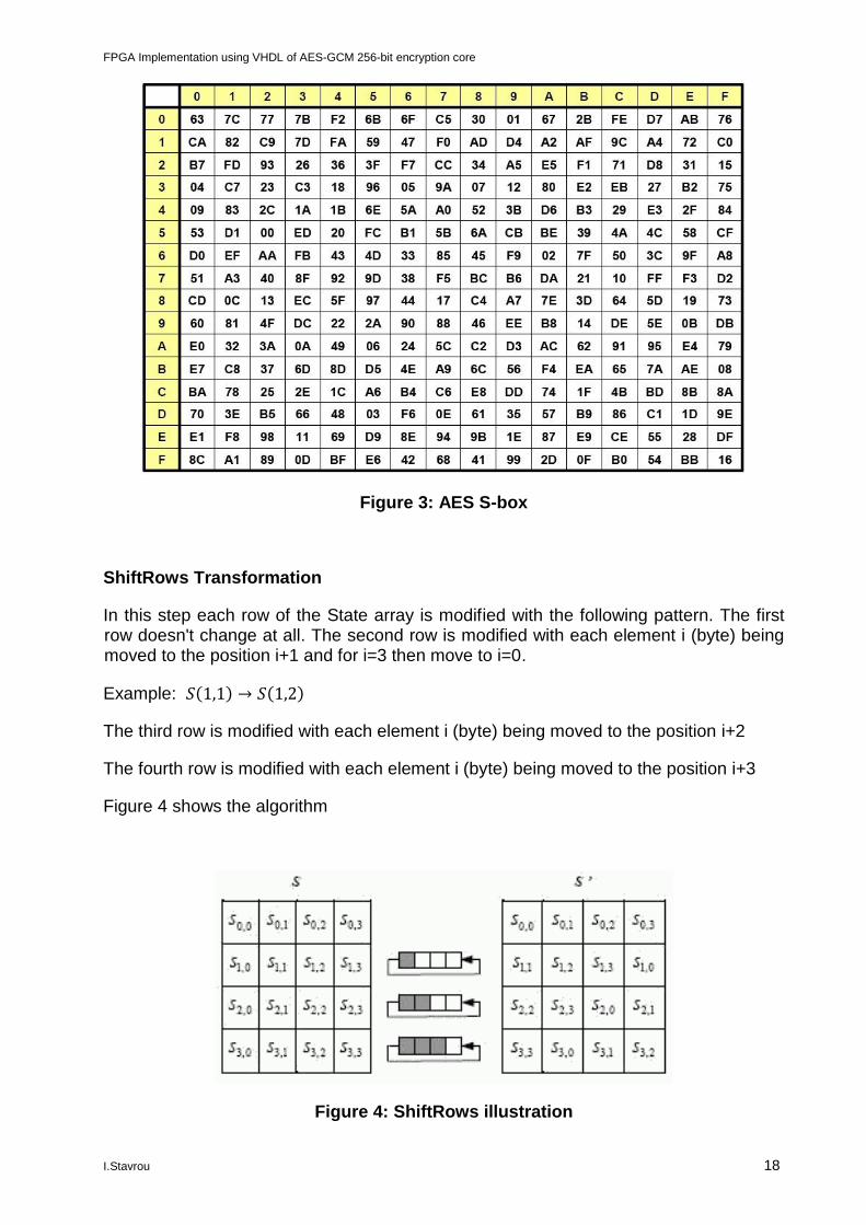
SubBytes Transformation
In this step a Non-Linear Transformation is applied on each byte with each byte from the S-box. The S-box is a look-up-table (LUT) created by a reversible array 16x16 with the 4 leftmost bits from each byte being used as row index and the 4 rightmost bits as column index.
The S-box used in the AES is illustrated in Figure 3
FPGA Implementation using VHDL of AES-GCM 256-bit encryption core
I.Stavrou 18
Figure 3: AES S-box
ShiftRows Transformation
In this step each row of the State array is modified with the following pattern. The first row doesn't change at all. The second row is modified with each element i (byte) being moved to the position i+1 and for i=3 then move to i=0.
Example: 𝑆(1,1) → 𝑆(1,2)
The third row is modified with each element i (byte) being moved to the position i+2
The fourth row is modified with each element i (byte) being moved to the position i+3
Figure 4 shows the algorithm
Figure 4: ShiftRows illustration
FPGA Implementation using VHDL of AES-GCM 256-bit encryption core
I.Stavrou 19
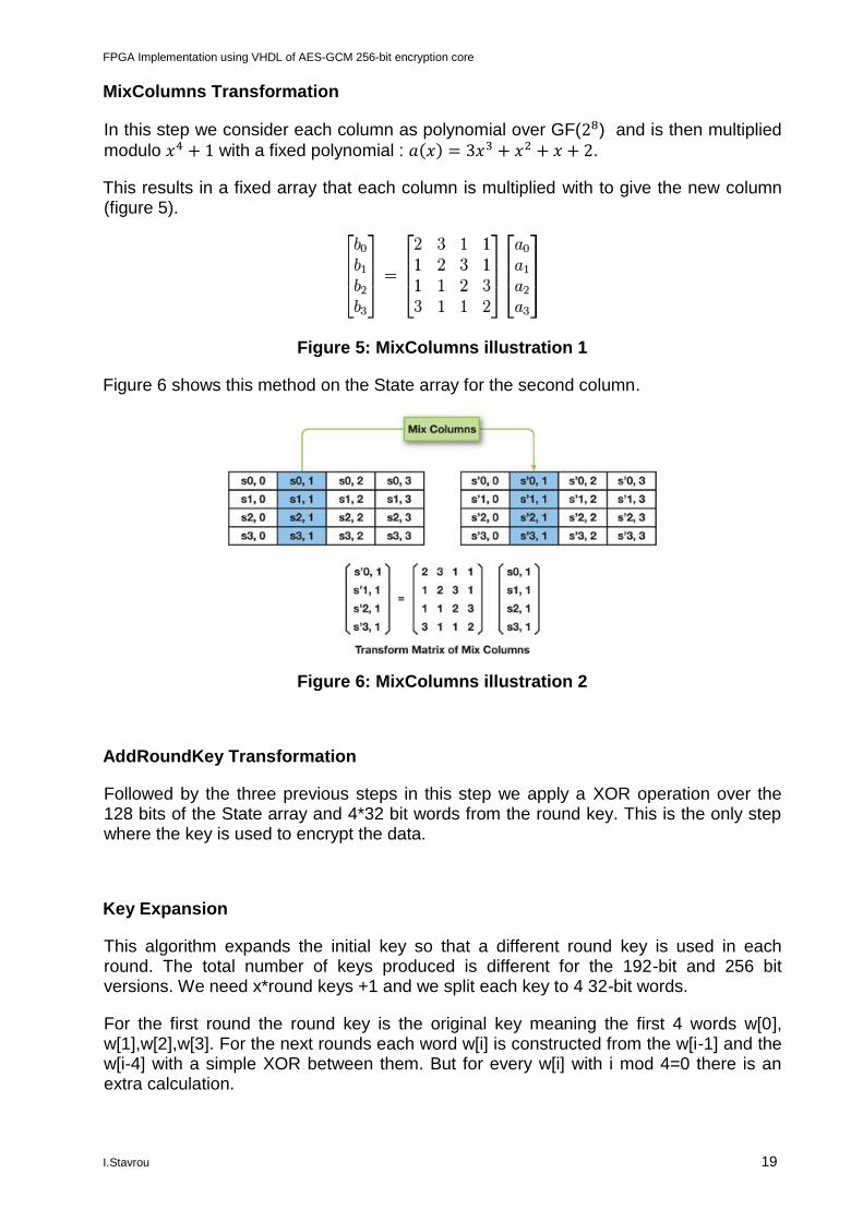
MixColumns Transformation
In this step we consider each column as polynomial over GF(28) and is then multiplied
modulo 𝑥4 + 1 with a fixed polynomial : 𝑎(𝑥) = 3𝑥3 + 𝑥2 + 𝑥 + 2.
This results in a fixed array that each column is multiplied with to give the new column (figure 5).
Figure 5: MixColumns illustration 1
Figure 6 shows this method on the State array for the second column.
Figure 6: MixColumns illustration 2
AddRoundKey Transformation
Followed by the three previous steps in this step we apply a XOR operation over the 128 bits of the State array and 4*32 bit words from the round key. This is the only step where the key is used to encrypt the data.
Key Expansion
This algorithm expands the initial key so that a different round key is used in each round. The total number of keys produced is different for the 192-bit and 256 bit versions. We need x*round keys +1 and we split each key to 4 32-bit words.
For the first round the round key is the original key meaning the first 4 words w[0], w[1],w[2],w[3]. For the next rounds each word w[i] is constructed from the w[i-1] and the w[i-4] with a simple XOR between them. But for every w[i] with i mod 4=0 there is an extra calculation.
FPGA Implementation using VHDL of AES-GCM 256-bit encryption core
I.Stavrou 20
For every w[i] with i mod 4 =0:
w[i] = ((w[i-4]) S-box (RotWord(w[i-1]))) XOR (Rcon)
-RotWord : Rotates a word transferring byte in position 0 to 4 and moving all other bytes a step left (RotWord(w[0],w[1],w[2],w[3]) = w[1],w[2],w[3],w[0])
-SubWord: Substitutes each byte from w[i-4] to each byte from RotWord(w[i-1]).
-Rcon: Rcon stands for round constant and it's a constant with 3 rightmost bits always 0.
3.3 GCM functions
GHASH
The GHASH function is defined by 𝐺𝐻𝐴𝑆𝐻(𝐻, 𝐴, 𝐶) = 𝑋𝑚+𝑛+1 where H is the Hash key, A is ADD which are not encrypted and C is the cipher text. The variable 𝑋𝑚+𝑛+1 is defined as:
where 𝑚 is the number of 128 bit blocks in A , 𝑛 is the number of 128 bit blocks in C , 𝜐 is the bit length of final block of A and 𝑢 is the bit length of final block of C. This is an
iterative algorithm where each 𝑋𝑖 depends on 𝑋𝑖−1 and the final 𝑋𝑖 is the output.
Multiplication (𝑿 ∙ 𝒀)
The • operation on (pairs of) the 2128 possible blocks corresponds to the multiplication
operation for the binary Galois (finite) field of 2128 elements. The 𝐺𝐹(2128) field used is
defined by the polynomial 𝑥128 + 𝑥7 + 𝑥2 + 𝑥 + 1. The following algorithm is defined by NIST SP-800-38D for the multiplication process.
Algorithm: X •Y
Input:
Block X, Y.
Output:
Block X •Y.
FPGA Implementation using VHDL of AES-GCM 256-bit encryption core
I.Stavrou 21
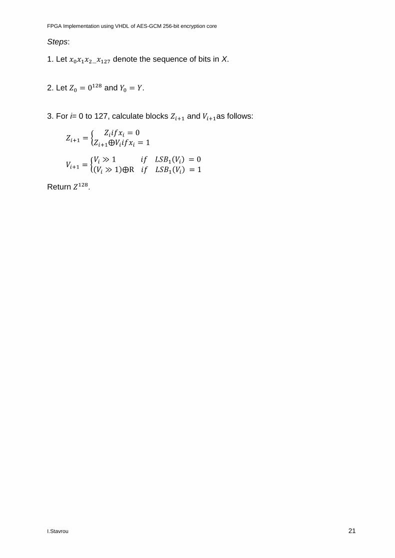
Steps:
1. Let 𝑥0𝑥1𝑥2…𝑥127 denote the sequence of bits in X.
2. Let 𝑍0 = 0128 and 𝑌0 = 𝑌.
3. For i= 0 to 127, calculate blocks 𝑍𝑖+1 and 𝑉𝑖+1as follows:
𝑍𝑖+1 = 𝑍𝑖𝑖𝑓𝑥𝑖 = 0
𝑍𝑖+1⨁𝑉𝑖𝑖𝑓𝑥𝑖 = 1
𝑉𝑖+1 = 𝑉𝑖 ≫ 1 𝑖𝑓 𝐿𝑆𝐵1(𝑉𝑖) = 0(𝑉𝑖 ≫ 1)⨁R 𝑖𝑓 𝐿𝑆𝐵1(𝑉𝑖) = 1
Return 𝑍128.
FPGA Implementation using VHDL of AES-GCM 256-bit encryption core
I.Stavrou 22
4. DESIGN OF AES-GCM-256
In this chapter, we analyze the algorithm steps and the limitations we have on a hardware implementation for the encryption process. In AES-GCM algorithm, AES core and GHASH core are the basic modules which are responsible for confidentiality and authentication, respectively. In chapter 4.1 we present the AES module and its parameters; in chapter 4.2 we present the GHASH module. The hardware implementation is presented in chapter 4.
4.1 AES Module
The AES module implements the AES algorithm for encryption at 256 bits. The signals inputs are a 256-bit key that is used for encryption, the data to be encrypted at 128 bits and the function control signal including a clock signal, a reset button and a start button. The output signals are the data ciphered at 128 bits, same as data input, and a done button that indicates the completion of the process.
4.1.1 Key Scheduler Module
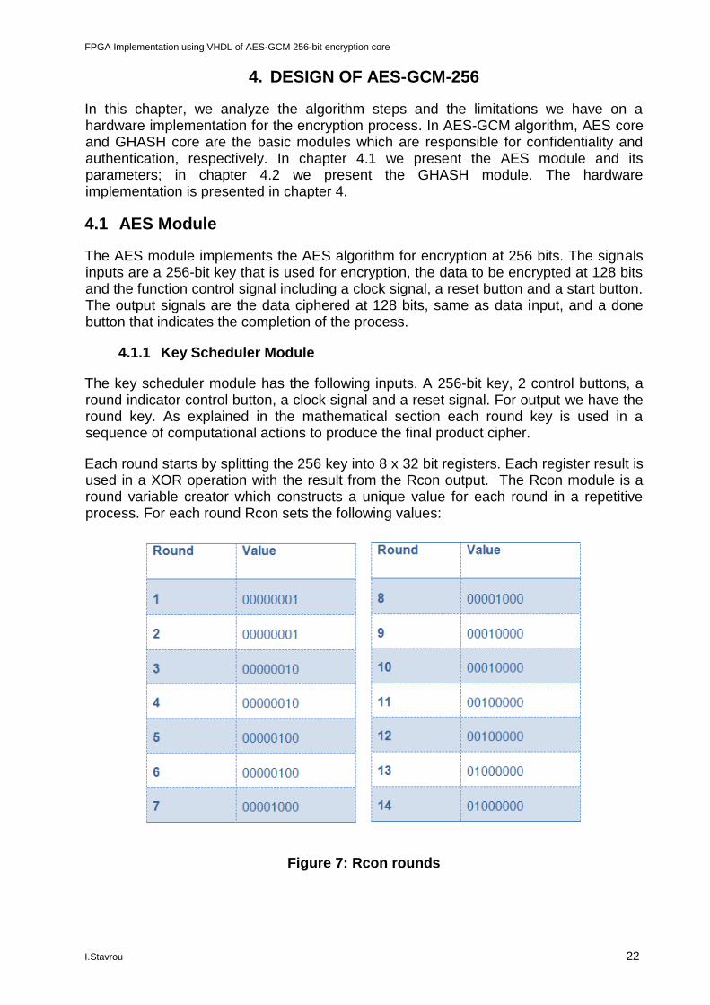
The key scheduler module has the following inputs. A 256-bit key, 2 control buttons, a round indicator control button, a clock signal and a reset signal. For output we have the round key. As explained in the mathematical section each round key is used in a sequence of computational actions to produce the final product cipher.
Each round starts by splitting the 256 key into 8 x 32 bit registers. Each register result is used in a XOR operation with the result from the Rcon output. The Rcon module is a round variable creator which constructs a unique value for each round in a repetitive process. For each round Rcon sets the following values:
Figure 7: Rcon rounds
FPGA Implementation using VHDL of AES-GCM 256-bit encryption core
I.Stavrou 23
Those values are expanded with the 24 left most bits of value “0”. The result is used to a XOR operation with the result from the S-Box. This output is used in a XOR operation with the first register feedback output following the second register which uses the result of the first register etc. creating a chain of sequential calculations.
The output of the algorithm is a 128-bit round key which is used in a XOR operation with the plain text to produce the round cipher. The round cipher is then used as input for the next round. For the round key we use the first 4 registers for odd number of rounds and the last 4 registers for even number of rounds, meaning that we use a feedback mechanism for the 256-bit key.
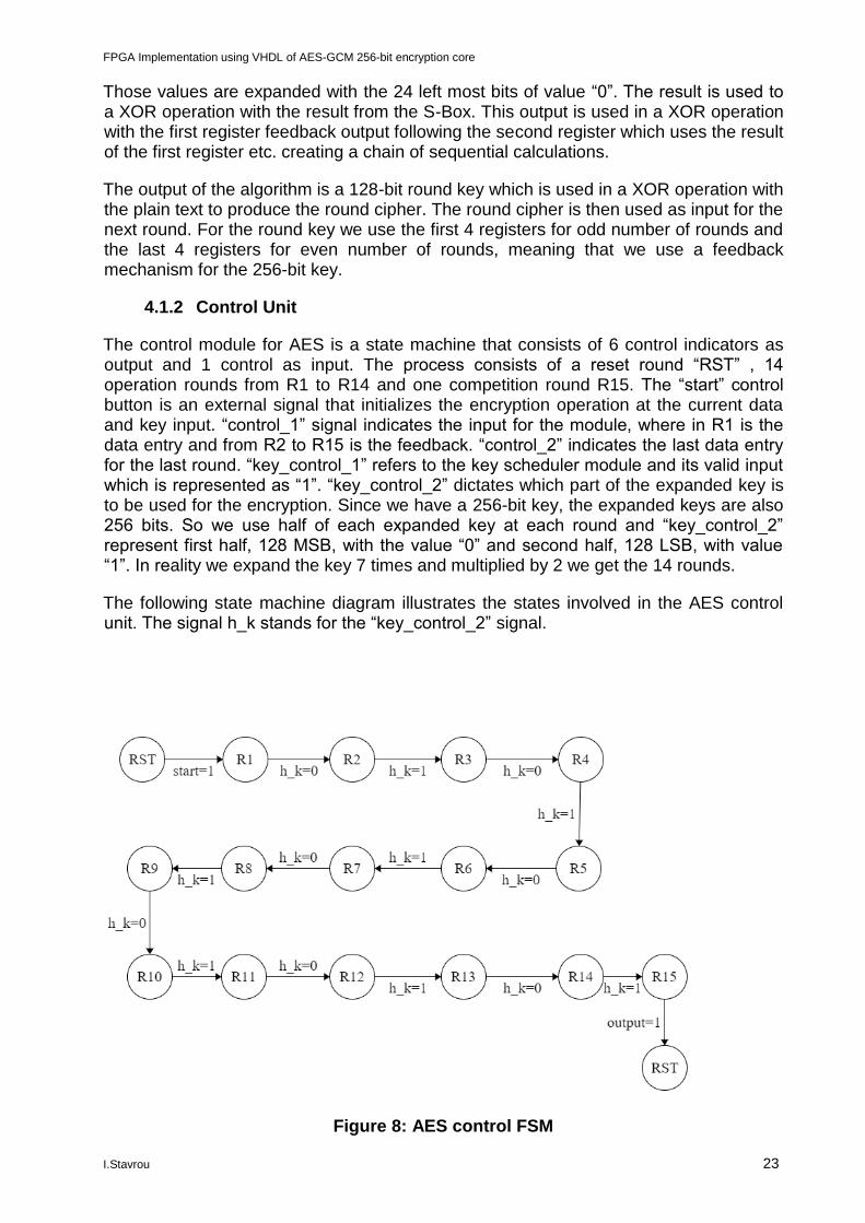
4.1.2 Control Unit
The control module for AES is a state machine that consists of 6 control indicators as output and 1 control as input. The process consists of a reset round “RST” , 14 operation rounds from R1 to R14 and one competition round R15. The “start” control button is an external signal that initializes the encryption operation at the current data and key input. “control_1” signal indicates the input for the module, where in R1 is the data entry and from R2 to R15 is the feedback. “control_2” indicates the last data entry for the last round. “key_control_1” refers to the key scheduler module and its valid input which is represented as “1”. “key_control_2” dictates which part of the expanded key is to be used for the encryption. Since we have a 256-bit key, the expanded keys are also 256 bits. So we use half of each expanded key at each round and “key_control_2” represent first half, 128 MSB, with the value “0” and second half, 128 LSB, with value “1”. In reality we expand the key 7 times and multiplied by 2 we get the 14 rounds.
The following state machine diagram illustrates the states involved in the AES control unit. The signal h_k stands for the “key_control_2” signal.
Figure 8: AES control FSM
FPGA Implementation using VHDL of AES-GCM 256-bit encryption core
I.Stavrou 24
4.2 GCM Module
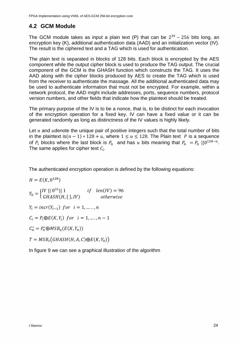
The GCM module takes as input a plain text (P) that can be 239 − 256 bits long, an encryption key (K), additional authentication data (AAD) and an initialization vector (IV). The result is the ciphered text and a TAG which is used for authentication.
The plain text is separated in blocks of 128 bits. Each block is encrypted by the AES component while the output cipher block is used to produce the TAG output. The crucial component of the GCM is the GHASH function which constructs the TAG. It uses the AAD along with the cipher blocks produced by AES to create the TAG which is used from the receiver to authenticate the massage. All the additional authenticated data may be used to authenticate information that must not be encrypted. For example, within a network protocol, the AAD might include addresses, ports, sequence numbers, protocol version numbers, and other fields that indicate how the plaintext should be treated.
The primary purpose of the IV is to be a nonce, that is, to be distinct for each invocation of the encryption operation for a fixed key. IV can have a fixed value or it can be generated randomly as long as distinctness of the IV values is highly likely.
Let 𝑛 and 𝑢denote the unique pair of positive integers such that the total number of bits in the plaintext is(𝑛 − 1) ∗ 128 + 𝑢, where 1 ≤ 𝑢 ≤ 128. The Plain text 𝑃 is a sequence
of 𝑃𝑖 blocks where the last block is 𝑃𝑛 and has 𝑢 bits meaning that 𝑃𝑛 = 𝑃𝑛 ||0128−𝑢.
The same applies for cipher text 𝐶𝑖.
The authenticated encryption operation is defined by the following equations:
𝐻 = 𝐸(𝐾, 0128)
𝑌0 = 𝐼𝑉 || 031|| 1 𝑖𝑓 𝑙𝑒𝑛(𝐼𝑉) = 96
𝐺𝐻𝐴𝑆𝐻(𝐻, , 𝐼𝑉) 𝑜𝑡ℎ𝑒𝑟𝑤𝑖𝑠𝑒
𝑌𝑖 = 𝑖𝑛𝑐𝑟(𝑌𝑖−1) 𝑓𝑜𝑟 𝑖 = 1, … . . , 𝑛
𝐶𝑖 = 𝑃𝑖⨁𝐸(𝐾, 𝑌𝑖) 𝑓𝑜𝑟 𝑖 = 1, … . , 𝑛 − 1
𝐶𝑛∗ = 𝑃𝑛
∗⨁𝑀𝑆𝐵𝑢(𝐸(𝐾, 𝑌𝑛))
𝑇 = 𝑀𝑆𝐵𝑡(𝐺𝐻𝐴𝑆𝐻(𝐻, 𝐴, 𝐶)⨁𝐸(𝐾, 𝑌0))
In figure 9 we can see a graphical illustration of the algorithm
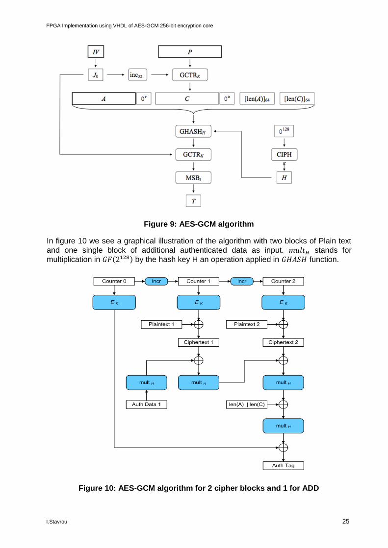
FPGA Implementation using VHDL of AES-GCM 256-bit encryption core
I.Stavrou 25
Figure 9: AES-GCM algorithm
In figure 10 we see a graphical illustration of the algorithm with two blocks of Plain text
and one single block of additional authenticated data as input. 𝑚𝑢𝑙𝑡𝐻 stands for
multiplication in 𝐺𝐹(2128) by the hash key H an operation applied in 𝐺𝐻𝐴𝑆𝐻 function.
Figure 10: AES-GCM algorithm for 2 cipher blocks and 1 for ADD
FPGA Implementation using VHDL of AES-GCM 256-bit encryption core
I.Stavrou 26
4.2.1 GF multiplier
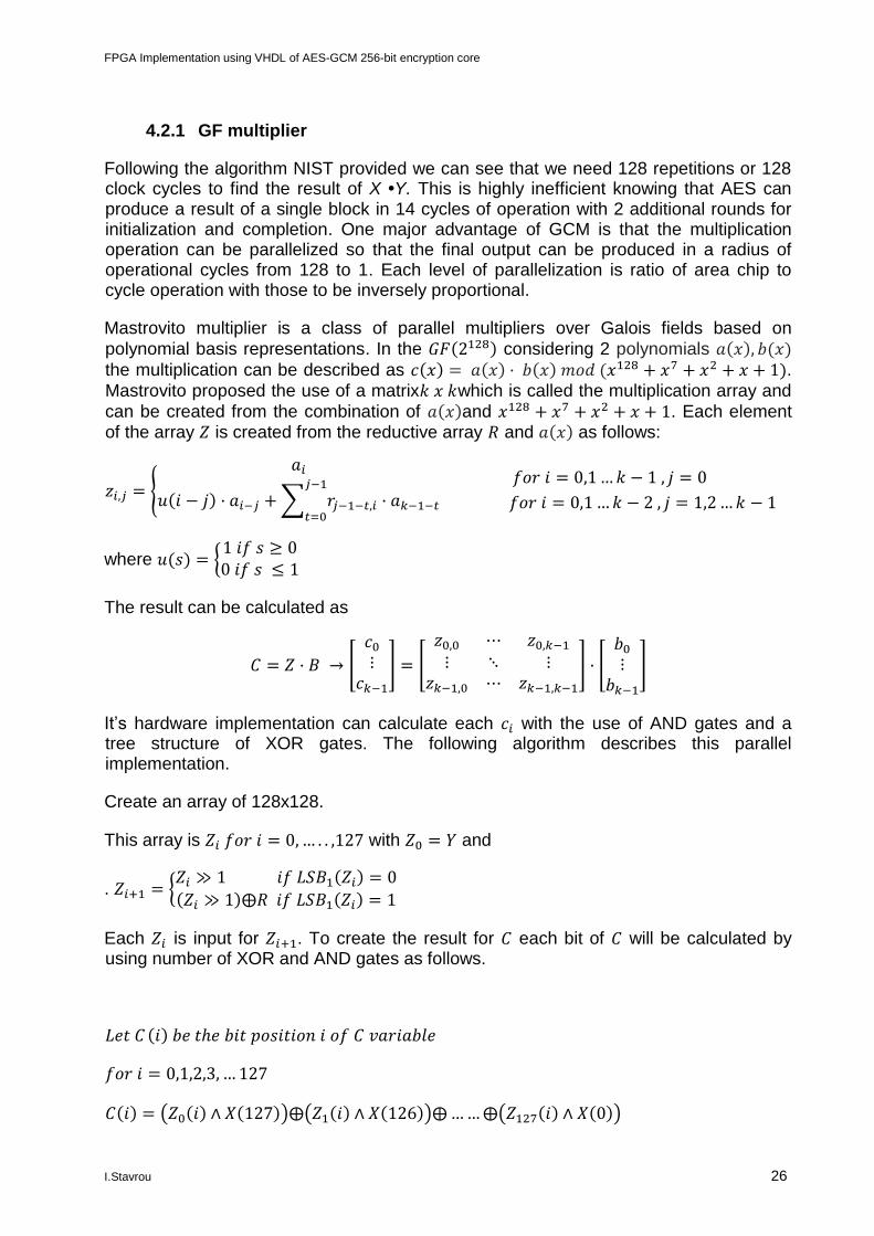
Following the algorithm NIST provided we can see that we need 128 repetitions or 128 clock cycles to find the result of X •Y. This is highly inefficient knowing that AES can produce a result of a single block in 14 cycles of operation with 2 additional rounds for initialization and completion. One major advantage of GCM is that the multiplication operation can be parallelized so that the final output can be produced in a radius of operational cycles from 128 to 1. Each level of parallelization is ratio of area chip to cycle operation with those to be inversely proportional.
Mastrovito multiplier is a class of parallel multipliers over Galois fields based on
polynomial basis representations. In the 𝐺𝐹(2128) considering 2 polynomials 𝑎(𝑥), 𝑏(𝑥)
the multiplication can be described as 𝑐(𝑥) = 𝑎(𝑥) · 𝑏(𝑥) 𝑚𝑜𝑑 (𝑥128 + 𝑥7 + 𝑥2 + 𝑥 + 1).
Mastrovito proposed the use of a matrix𝑘 𝑥 𝑘which is called the multiplication array and
can be created from the combination of 𝑎(𝑥)and 𝑥128 + 𝑥7 + 𝑥2 + 𝑥 + 1. Each element of the array 𝑍 is created from the reductive array 𝑅 and 𝑎(𝑥) as follows:
𝑧𝑖,𝑗 =
𝑎𝑖
𝑢(𝑖 − 𝑗) · 𝑎𝑖−𝑗 + ∑ 𝑟𝑗−1−𝑡,𝑖 · 𝑎𝑘−1−𝑡
𝑗−1
𝑡=0
𝑓𝑜𝑟 𝑖 = 0,1 … 𝑘 − 1 , 𝑗 = 0
𝑓𝑜𝑟 𝑖 = 0,1 … 𝑘 − 2 , 𝑗 = 1,2 … 𝑘 − 1
where 𝑢(𝑠) = 1 𝑖𝑓 𝑠 ≥ 00 𝑖𝑓 𝑠 ≤ 1
The result can be calculated as
𝐶 = 𝑍 · 𝐵 → [
𝑐0
⋮𝑐𝑘−1
] = [
𝑧0,0 ⋯ 𝑧0,𝑘−1
⋮ ⋱ ⋮𝑧𝑘−1,0 ⋯ 𝑧𝑘−1,𝑘−1
] · [𝑏0
⋮𝑏𝑘−1
]
It’s hardware implementation can calculate each 𝑐𝑖 with the use of AND gates and a tree structure of XOR gates. The following algorithm describes this parallel implementation.
Create an array of 128x128.
This array is 𝑍𝑖 𝑓𝑜𝑟 𝑖 = 0, … . . ,127 with 𝑍0 = 𝑌 and
. 𝑍𝑖+1 = 𝑍𝑖 ≫ 1 𝑖𝑓 𝐿𝑆𝐵1(𝑍𝑖) = 0(𝑍𝑖 ≫ 1)⨁𝑅 𝑖𝑓 𝐿𝑆𝐵1(𝑍𝑖) = 1
Each 𝑍𝑖 is input for 𝑍𝑖+1. To create the result for 𝐶 each bit of 𝐶 will be calculated by using number of XOR and AND gates as follows.
𝐿𝑒𝑡 𝐶 (𝑖) 𝑏𝑒 𝑡ℎ𝑒 𝑏𝑖𝑡 𝑝𝑜𝑠𝑖𝑡𝑖𝑜𝑛 𝑖 𝑜𝑓 𝐶 𝑣𝑎𝑟𝑖𝑎𝑏𝑙𝑒
𝑓𝑜𝑟 𝑖 = 0,1,2,3, … 127
𝐶(𝑖) = (𝑍0(𝑖) ∧ 𝑋(127))⨁(𝑍1(𝑖) ∧ 𝑋(126))⨁ … … ⨁(𝑍127(𝑖) ∧ 𝑋(0))
FPGA Implementation using VHDL of AES-GCM 256-bit encryption core
I.Stavrou 27
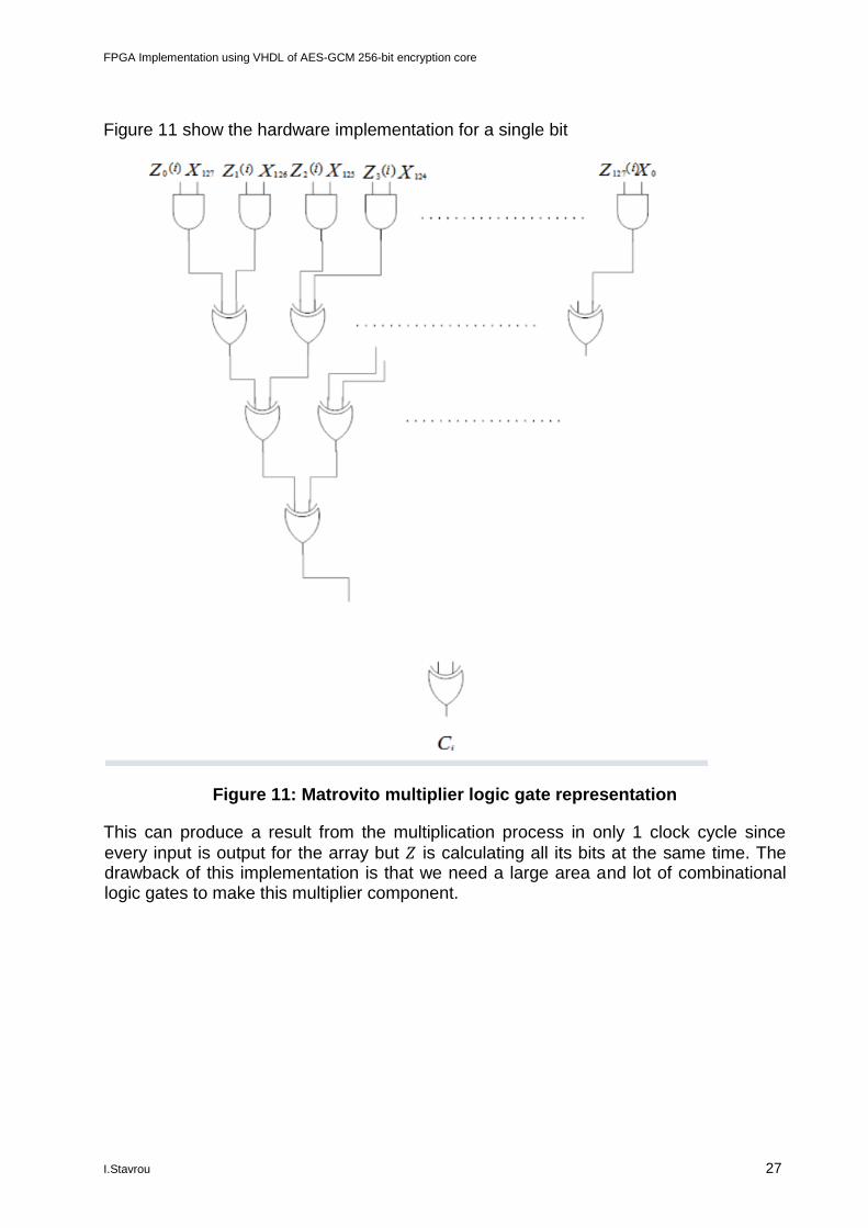
Figure 11 show the hardware implementation for a single bit
Figure 11: Matrovito multiplier logic gate representation
This can produce a result from the multiplication process in only 1 clock cycle since
every input is output for the array but 𝑍 is calculating all its bits at the same time. The drawback of this implementation is that we need a large area and lot of combinational logic gates to make this multiplier component.
FPGA Implementation using VHDL of AES-GCM 256-bit encryption core
I.Stavrou 28
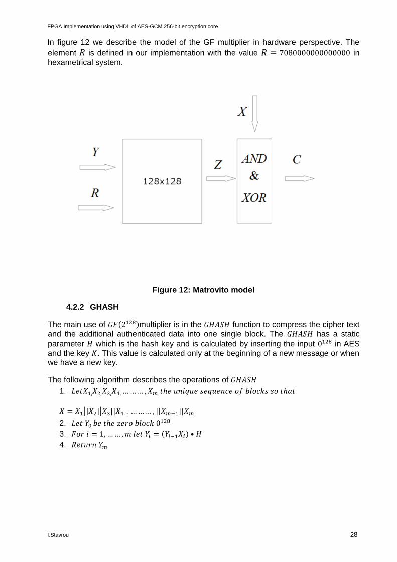
In figure 12 we describe the model of the GF multiplier in hardware perspective. The
element 𝑅 is defined in our implementation with the value 𝑅 = 7080000000000000 in
hexametrical system.
Figure 12: Matrovito model
4.2.2 GHASH
The main use of 𝐺𝐹(2128)multiplier is in the 𝐺𝐻𝐴𝑆𝐻 function to compress the cipher text and the additional authenticated data into one single block. The 𝐺𝐻𝐴𝑆𝐻 has a static
parameter 𝐻 which is the hash key and is calculated by inserting the input 0128 in AES
and the key 𝐾. This value is calculated only at the beginning of a new message or when we have a new key.
The following algorithm describes the operations of 𝐺𝐻𝐴𝑆𝐻
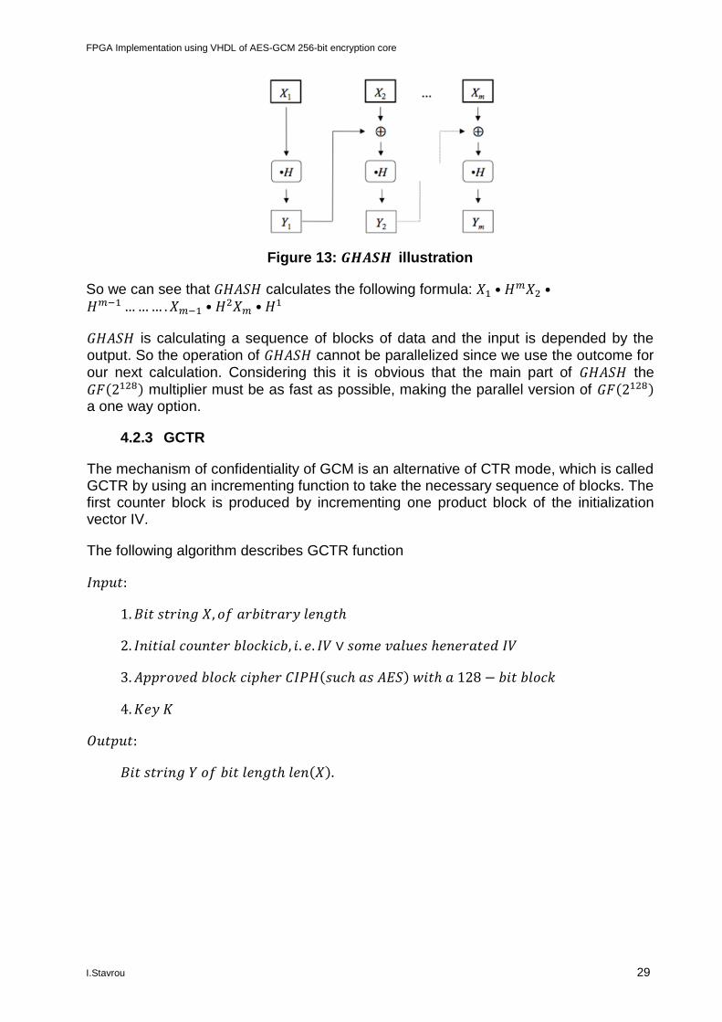
1. 𝐿𝑒𝑡𝑋1,𝑋2,𝑋3,𝑋4, … … … , 𝑋𝑚 𝑡ℎ𝑒 𝑢𝑛𝑖𝑞𝑢𝑒 𝑠𝑒𝑞𝑢𝑒𝑛𝑐𝑒 𝑜𝑓 𝑏𝑙𝑜𝑐𝑘𝑠 𝑠𝑜 𝑡ℎ𝑎𝑡
𝑋 = 𝑋1||𝑋2||𝑋3||𝑋4 , … … … , ||𝑋𝑚−1||𝑋𝑚
2. 𝐿𝑒𝑡 𝑌0 𝑏𝑒 𝑡ℎ𝑒 𝑧𝑒𝑟𝑜 𝑏𝑙𝑜𝑐𝑘 0128
3. 𝐹𝑜𝑟 𝑖 = 1, … … , 𝑚 𝑙𝑒𝑡 𝑌𝑖 = (𝑌𝑖−1𝑋𝑖) • 𝐻
4. 𝑅𝑒𝑡𝑢𝑟𝑛 𝑌𝑚
FPGA Implementation using VHDL of AES-GCM 256-bit encryption core
I.Stavrou 29
Figure 13: 𝑮𝑯𝑨𝑺𝑯 illustration
So we can see that 𝐺𝐻𝐴𝑆𝐻 calculates the following formula: 𝑋1 • 𝐻𝑚𝑋2 •𝐻𝑚−1 … … … . 𝑋𝑚−1 • 𝐻2𝑋𝑚 • 𝐻1
𝐺𝐻𝐴𝑆𝐻 is calculating a sequence of blocks of data and the input is depended by the output. So the operation of 𝐺𝐻𝐴𝑆𝐻 cannot be parallelized since we use the outcome for our next calculation. Considering this it is obvious that the main part of 𝐺𝐻𝐴𝑆𝐻 the
𝐺𝐹(2128) multiplier must be as fast as possible, making the parallel version of 𝐺𝐹(2128) a one way option.
4.2.3 GCTR
The mechanism of confidentiality of GCM is an alternative of CTR mode, which is called GCTR by using an incrementing function to take the necessary sequence of blocks. The first counter block is produced by incrementing one product block of the initialization vector IV.
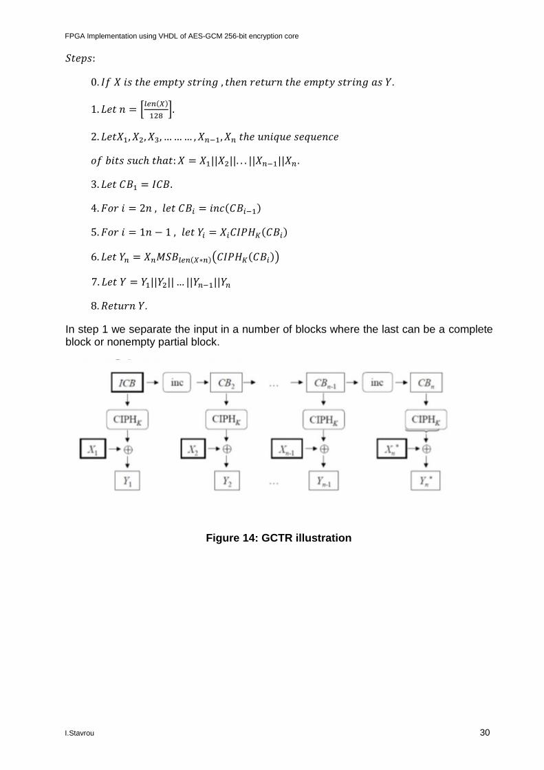
The following algorithm describes GCTR function
𝐼𝑛𝑝𝑢𝑡:
1. 𝐵𝑖𝑡 𝑠𝑡𝑟𝑖𝑛𝑔 𝑋, 𝑜𝑓 𝑎𝑟𝑏𝑖𝑡𝑟𝑎𝑟𝑦 𝑙𝑒𝑛𝑔𝑡ℎ
2. 𝐼𝑛𝑖𝑡𝑖𝑎𝑙 𝑐𝑜𝑢𝑛𝑡𝑒𝑟 𝑏𝑙𝑜𝑐𝑘𝑖𝑐𝑏, 𝑖. 𝑒. 𝐼𝑉 ∨ 𝑠𝑜𝑚𝑒 𝑣𝑎𝑙𝑢𝑒𝑠 ℎ𝑒𝑛𝑒𝑟𝑎𝑡𝑒𝑑 𝐼𝑉
3. 𝐴𝑝𝑝𝑟𝑜𝑣𝑒𝑑 𝑏𝑙𝑜𝑐𝑘 𝑐𝑖𝑝ℎ𝑒𝑟 𝐶𝐼𝑃𝐻(𝑠𝑢𝑐ℎ 𝑎𝑠 𝐴𝐸𝑆) 𝑤𝑖𝑡ℎ 𝑎 128 − 𝑏𝑖𝑡 𝑏𝑙𝑜𝑐𝑘
4. 𝐾𝑒𝑦 𝐾
𝑂𝑢𝑡𝑝𝑢𝑡:
𝐵𝑖𝑡 𝑠𝑡𝑟𝑖𝑛𝑔 𝑌 𝑜𝑓 𝑏𝑖𝑡 𝑙𝑒𝑛𝑔𝑡ℎ 𝑙𝑒𝑛(𝑋).
FPGA Implementation using VHDL of AES-GCM 256-bit encryption core
I.Stavrou 30
𝑆𝑡𝑒𝑝𝑠:
0. 𝐼𝑓 𝑋 𝑖𝑠 𝑡ℎ𝑒 𝑒𝑚𝑝𝑡𝑦 𝑠𝑡𝑟𝑖𝑛𝑔 , 𝑡ℎ𝑒𝑛 𝑟𝑒𝑡𝑢𝑟𝑛 𝑡ℎ𝑒 𝑒𝑚𝑝𝑡𝑦 𝑠𝑡𝑟𝑖𝑛𝑔 𝑎𝑠 𝑌.
1. 𝐿𝑒𝑡 𝑛 = [𝑙𝑒𝑛(𝑋)
128].
2. 𝐿𝑒𝑡𝑋1, 𝑋2, 𝑋3, … … … , 𝑋𝑛−1, 𝑋𝑛 𝑡ℎ𝑒 𝑢𝑛𝑖𝑞𝑢𝑒 𝑠𝑒𝑞𝑢𝑒𝑛𝑐𝑒
𝑜𝑓 𝑏𝑖𝑡𝑠 𝑠𝑢𝑐ℎ 𝑡ℎ𝑎𝑡: 𝑋 = 𝑋1||𝑋2||. . . ||𝑋𝑛−1||𝑋𝑛.
3. 𝐿𝑒𝑡 𝐶𝐵1 = 𝐼𝐶𝐵.
4. 𝐹𝑜𝑟 𝑖 = 2𝑛 , 𝑙𝑒𝑡 𝐶𝐵𝑖 = 𝑖𝑛𝑐(𝐶𝐵𝑖−1)
5. 𝐹𝑜𝑟 𝑖 = 1𝑛 − 1 , 𝑙𝑒𝑡 𝑌𝑖 = 𝑋𝑖𝐶𝐼𝑃𝐻𝐾(𝐶𝐵𝑖)
6. 𝐿𝑒𝑡 𝑌𝑛 = 𝑋𝑛𝑀𝑆𝐵𝑙𝑒𝑛(𝑋∗𝑛)(𝐶𝐼𝑃𝐻𝐾(𝐶𝐵𝑖))
7. 𝐿𝑒𝑡 𝑌 = 𝑌1||𝑌2|| … ||𝑌𝑛−1||𝑌𝑛
8. 𝑅𝑒𝑡𝑢𝑟𝑛 𝑌.
In step 1 we separate the input in a number of blocks where the last can be a complete block or nonempty partial block.
Figure 14: GCTR illustration
FPGA Implementation using VHDL of AES-GCM 256-bit encryption core
I.Stavrou 31
5. IMPLEMENTATION AND SIMULATION
The simulation process is the most important process in the design procedure and the most time consuming. It ensures that our system is functional and efficient, according to our design goals. Since we use a multi-level minimization approach on our design we must ensure that out bottom level components are simulated and optimized before we move to the next level. In this design we simulated the 2 key components AES to its upgraded version of 256-bit key size and GF multiplier. Finally, we simulated the complete design. The simulations of AES-256 and AES-GCM were completed using test vectors given by various online sources. At first, we analyze the upgraded aes-256 component with a test bench running on Isim. Then we analyze the GF multiplier and we apply a multiplication in a single clock cycle to achieve maximum efficiency using a parallel version of it. Finally, we simulate the complete design that implements the
𝐺𝐻𝐴𝑆𝐻 function and produces the TAG and uses the aes to make the cipher text.
5.1 AES-256
The main difference from version 128-bit to 256-bit is the number of rounds the algorithm needs to make the result. In the 128-bit version we need 10 rounds of data shuffling while in the 256-bit version we need 14 rounds. For this we need to change the design of key scheduler as was described in section 4.1.1. The key scheduler now takes the 256-bit key as input and it splits it into two 128 bit blocks one with the MSB and one with the LSB making the round key to be used. Following this step, the process on data is the same as the 128-bit version. We just add 4 more rounds to use all of our key products. The calculation of the new key round takes place every 2 rounds. We use the 128 LSB bits for the first round then the 128 MSB bits for the second round and then the process goes on with a new calculation for the next 2 rounds. The process ends at the 14 round where we have calculated a total of 7 different 256 bit keys, plus 2 more rounds for initialization and competition.
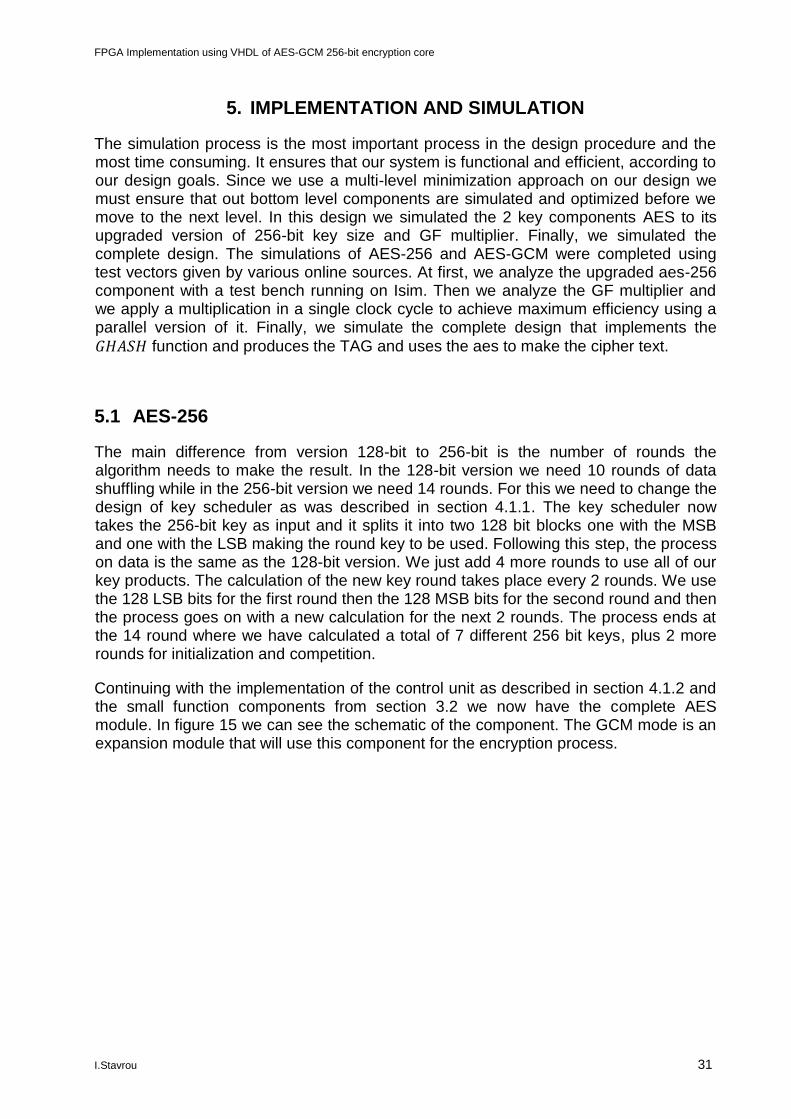
Continuing with the implementation of the control unit as described in section 4.1.2 and the small function components from section 3.2 we now have the complete AES module. In figure 15 we can see the schematic of the component. The GCM mode is an expansion module that will use this component for the encryption process.
FPGA Implementation using VHDL of AES-GCM 256-bit encryption core
I.Stavrou 32
Figure 15: AES schematic
FPGA Implementation using VHDL of AES-GCM 256-bit encryption core
I.Stavrou 33
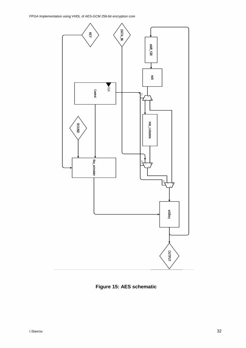
In figure 16 we can see the encryption process in a test bench.
Figure 16: AES test bench
We can see that seven 256 bit keys are produced and we use the 128 MSB and LSB results to use in 14 rounds with the 128-bit block data input to make the final result. At this point we understand that this is the minimum clock cycles we need in our design per data block. This sets our bottom boundary for our design to at least 14 rounds.
5.2 GF Multiplier
The next core component is the GF multiplier. Here we wanted the parallel version from the options described above to achieve 1 single cycle per multiplication. As described above the Mastrovito edition was a parallelized version suitable for this cause. We implemented a series of AND and XOR gates following the algorithm described in 4.2.1 creating a large combinational path were each bit of the output is calculated at the same time. While this is the largest combinational path in our design, the total delay is a small fraction of the delay we would have if we were using the multi cycle version.
Following the algorithm, we initialize an array of 128 vectors V, with every vector 128 bits long. V(0) equals input Y. Each V(i) vector is equal to V(i-1) right sifted by 1 bit when the rightmost of V(i) is equal to 0, or else is equal to V(i-1) right sifted by 1 bit and then a XOR operation is applied with the R vector. The R vector has a static value of 0x7080000000000000. Each bit of the output Z is described by the following procedure:
𝑍𝑖 = (𝑉𝑖(0) 𝐴𝑁𝐷 𝑋127) ⨁ (𝑉𝑖(1) 𝐴𝑁𝐷 𝑋126)⨁ (𝑉𝑖(2) 𝐴𝑁𝐷 𝑋125) … ⨁ (𝑉𝑖(127) 𝐴𝑁𝐷 𝑋0)
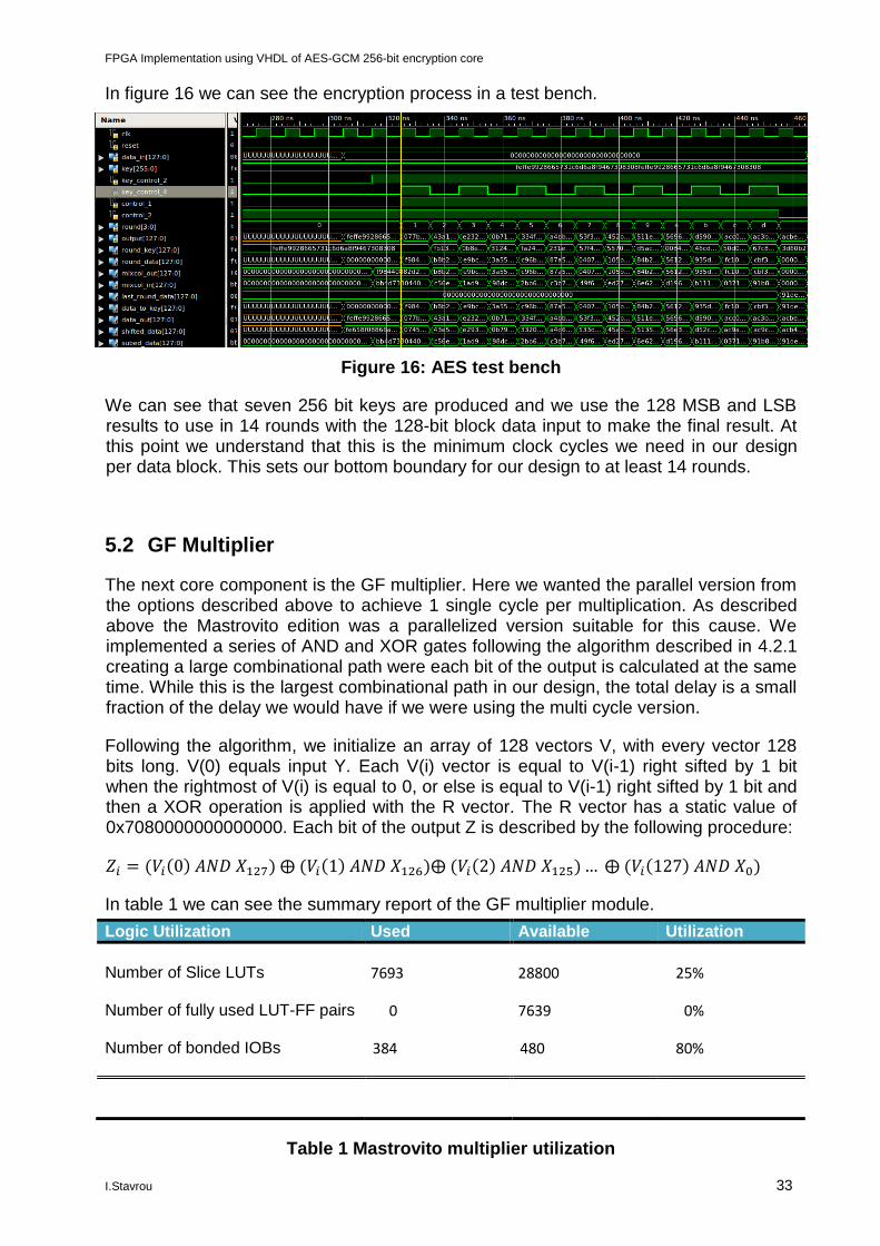
In table 1 we can see the summary report of the GF multiplier module.
Logic Utilization Used Available Utilization
Number of Slice LUTs 7693 28800 25%
Number of fully used LUT-FF pairs 0 7639 0%
Number of bonded IOBs 384 480 80%
Table 1 Mastrovito multiplier utilization
FPGA Implementation using VHDL of AES-GCM 256-bit encryption core
I.Stavrou 34
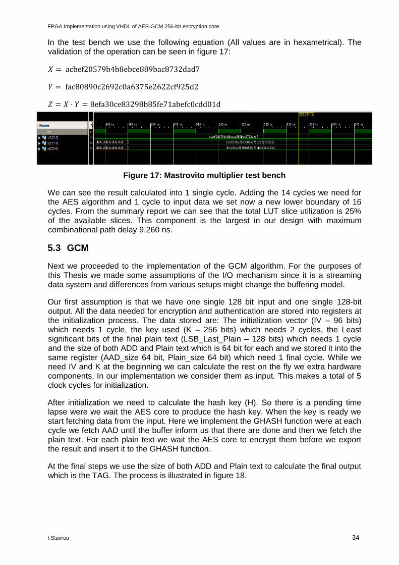
In the test bench we use the following equation (All values are in hexametrical). The validation of the operation can be seen in figure 17:
𝑋 = acbef20579b4b8ebce889bac8732dad7
𝑌 = fac80890c2692c0a6375e2622cf925d2
𝑍 = 𝑋 · 𝑌 = 8efa30ce83298b85fe71abefc0cdd01d
Figure 17: Mastrovito multiplier test bench
We can see the result calculated into 1 single cycle. Adding the 14 cycles we need for the AES algorithm and 1 cycle to input data we set now a new lower boundary of 16 cycles. From the summary report we can see that the total LUT slice utilization is 25% of the available slices. This component is the largest in our design with maximum combinational path delay 9.260 ns.
5.3 GCM
Next we proceeded to the implementation of the GCM algorithm. For the purposes of this Thesis we made some assumptions of the I/O mechanism since it is a streaming data system and differences from various setups might change the buffering model.
Our first assumption is that we have one single 128 bit input and one single 128-bit output. All the data needed for encryption and authentication are stored into registers at the initialization process. The data stored are: The initialization vector (IV – 96 bits) which needs 1 cycle, the key used (K – 256 bits) which needs 2 cycles, the Least significant bits of the final plain text (LSB_Last_Plain – 128 bits) which needs 1 cycle and the size of both ADD and Plain text which is 64 bit for each and we stored it into the same register (AAD_size 64 bit, Plain_size 64 bit) which need 1 final cycle. While we need IV and K at the beginning we can calculate the rest on the fly we extra hardware components. In our implementation we consider them as input. This makes a total of 5 clock cycles for initialization.
After initialization we need to calculate the hash key (H). So there is a pending time lapse were we wait the AES core to produce the hash key. When the key is ready we start fetching data from the input. Here we implement the GHASH function were at each cycle we fetch AAD until the buffer inform us that there are done and then we fetch the plain text. For each plain text we wait the AES core to encrypt them before we export the result and insert it to the GHASH function.
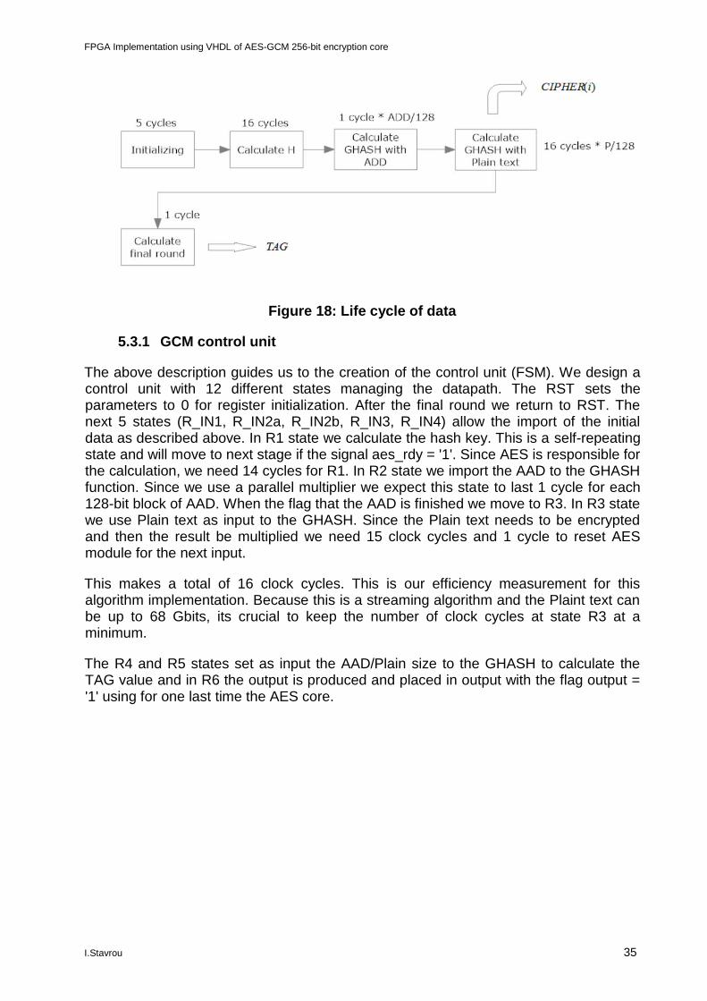
At the final steps we use the size of both ADD and Plain text to calculate the final output which is the TAG. The process is illustrated in figure 18.
FPGA Implementation using VHDL of AES-GCM 256-bit encryption core
I.Stavrou 35
Figure 18: Life cycle of data
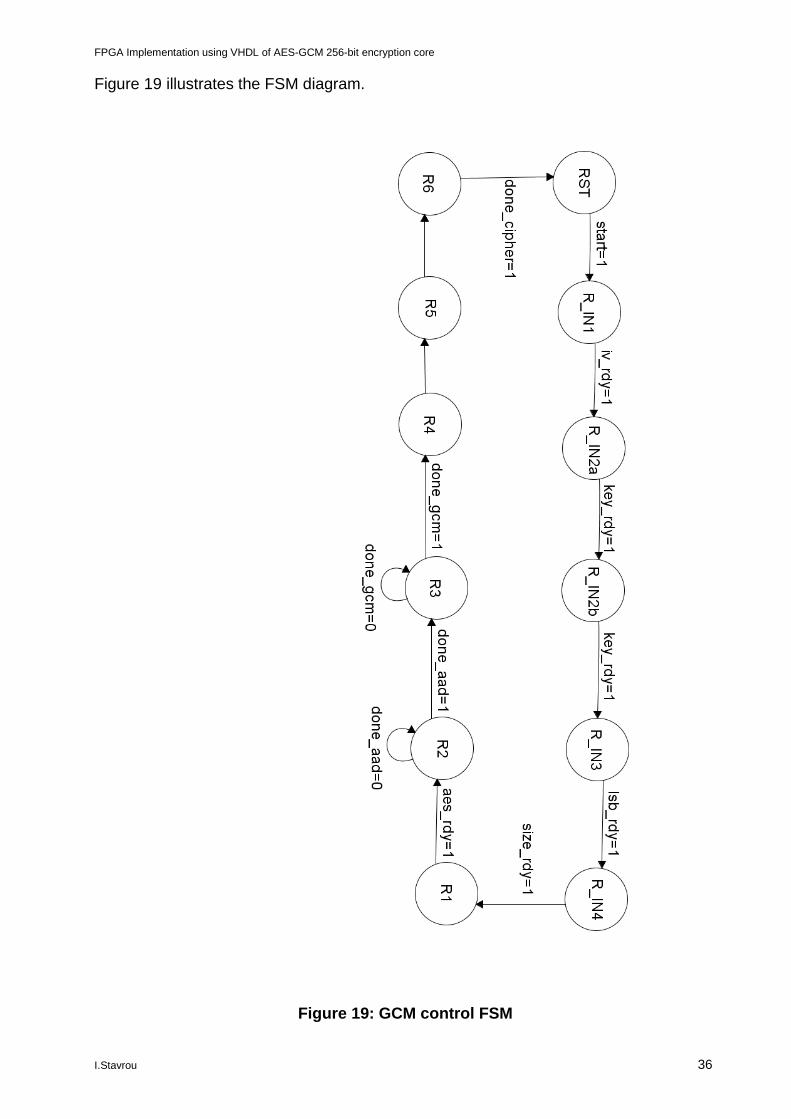
5.3.1 GCM control unit
The above description guides us to the creation of the control unit (FSM). We design a control unit with 12 different states managing the datapath. The RST sets the parameters to 0 for register initialization. After the final round we return to RST. The next 5 states (R_IN1, R_IN2a, R_IN2b, R_IN3, R_IN4) allow the import of the initial data as described above. In R1 state we calculate the hash key. This is a self-repeating state and will move to next stage if the signal aes_rdy = '1'. Since AES is responsible for the calculation, we need 14 cycles for R1. In R2 state we import the AAD to the GHASH function. Since we use a parallel multiplier we expect this state to last 1 cycle for each 128-bit block of AAD. When the flag that the AAD is finished we move to R3. In R3 state we use Plain text as input to the GHASH. Since the Plain text needs to be encrypted and then the result be multiplied we need 15 clock cycles and 1 cycle to reset AES module for the next input.
This makes a total of 16 clock cycles. This is our efficiency measurement for this algorithm implementation. Because this is a streaming algorithm and the Plaint text can be up to 68 Gbits, its crucial to keep the number of clock cycles at state R3 at a minimum.
The R4 and R5 states set as input the AAD/Plain size to the GHASH to calculate the TAG value and in R6 the output is produced and placed in output with the flag output = '1' using for one last time the AES core.
FPGA Implementation using VHDL of AES-GCM 256-bit encryption core
I.Stavrou 36
Figure 19 illustrates the FSM diagram.
Figure 19: GCM control FSM
FPGA Implementation using VHDL of AES-GCM 256-bit encryption core
I.Stavrou 37
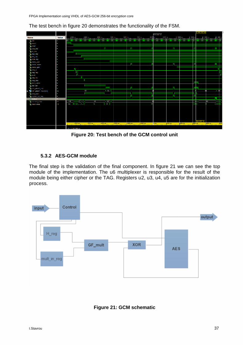
The test bench in figure 20 demonstrates the functionality of the FSM.
Figure 20: Test bench of the GCM control unit
5.3.2 AES-GCM module
The final step is the validation of the final component. In figure 21 we can see the top module of the implementation. The u6 multiplexer is responsible for the result of the module being either cipher or the TAG. Registers u2, u3, u4, u5 are for the initialization process.
Figure 21: GCM schematic
FPGA Implementation using VHDL of AES-GCM 256-bit encryption core
I.Stavrou 38
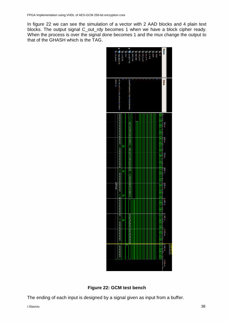
In figure 22 we can see the simulation of a vector with 2 AAD blocks and 4 plain text blocks. The output signal C_out_rdy becomes 1 when we have a block cipher ready. When the process is over the signal done becomes 1 and the mux change the output to that of the GHASH which is the TAG.
Figure 22: GCM test bench
The ending of each input is designed by a signal given as input from a buffer.
FPGA Implementation using VHDL of AES-GCM 256-bit encryption core
I.Stavrou 39
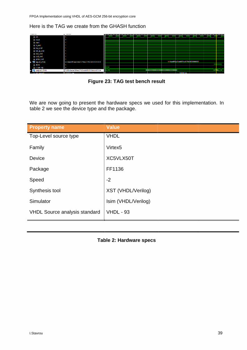
Here is the TAG we create from the GHASH function
Figure 23: TAG test bench result
We are now going to present the hardware specs we used for this implementation. In table 2 we see the device type and the package.
Property name Value
Top-Level source type VHDL
Family Virtex5
Device XC5VLX50T
Package FF1136
Speed -2
Synthesis tool XST (VHDL/Verilog)
Simulator Isim (VHDL/Verilog)
VHDL Source analysis standard VHDL - 93
Table 2: Hardware specs
FPGA Implementation using VHDL of AES-GCM 256-bit encryption core
I.Stavrou 40
From the synthesis tools we have produced the timing and memory report presented in table 3.
Property name Value
Speed Grade -2
Minimum period 4.392 ns
Maximum Frequency 227.690 Mhz
Minimum input arrival time before clock 3.643 ns
Maximum output required time after clock 6.662 ns
Maximum combinational path delay 6.605 ns
Total memory usage 538016 KB
Table 3: Timing and memory report
In table 4 we can see the total utilization of the device.
Logic Utilization Used Available Utilization
Number of Slice Registers 1660 28800 5%
Number of Slice LUTs 10126 28800 35%
Number of fully used LUT-FF pairs 967 10819 8%
Number of bonded IOBs 267 480 55%
Number of block of RAM/FIFO 1 60 1%
Number of BUFG/BUFGCTRLs 1 32 3%
Table 4: Total utilization
We achieved a Minimum period of 4.392 ns with 16 clock cycles for processing a single plain text block. With a pipelined version we can achieve even greater results up to 1 clock cycle if we use 16 AES cores. This would require a large number of slice LUTs, were in our device we can use up to 3. But those improvements, which would allow processing 68Gbps in less than 10 seconds, are of small importance since the buffering system cannot support speeds not even close to that though limiting the potential of the FPGA.
FPGA Implementation using VHDL of AES-GCM 256-bit encryption core
I.Stavrou 41
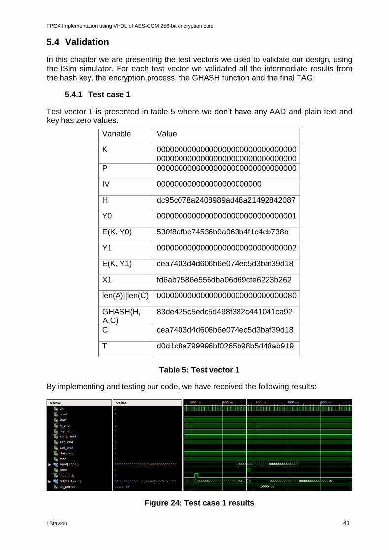
5.4 Validation
In this chapter we are presenting the test vectors we used to validate our design, using the ISim simulator. For each test vector we validated all the intermediate results from the hash key, the encryption process, the GHASH function and the final TAG.
5.4.1 Test case 1
Test vector 1 is presented in table 5 where we don’t have any AAD and plain text and key has zero values.
Variable Value
K 00000000000000000000000000000000 00000000000000000000000000000000
P 00000000000000000000000000000000
IV 000000000000000000000000
H dc95c078a2408989ad48a21492842087
Y0 00000000000000000000000000000001
E(K, Y0) 530f8afbc74536b9a963b4f1c4cb738b
Y1 00000000000000000000000000000002
E(K, Y1) cea7403d4d606b6e074ec5d3baf39d18
X1 fd6ab7586e556dba06d69cfe6223b262
len(A)||len(C) 00000000000000000000000000000080
GHASH(H, A,C)
83de425c5edc5d498f382c441041ca92
C cea7403d4d606b6e074ec5d3baf39d18
T d0d1c8a799996bf0265b98b5d48ab919
Table 5: Test vector 1
By implementing and testing our code, we have received the following results:
Figure 24: Test case 1 results
FPGA Implementation using VHDL of AES-GCM 256-bit encryption core
I.Stavrou 42
5.4.2 Test case 2
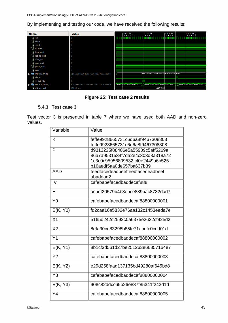
Test vector 2 is presented in table 6 where we don’t have AAD, but we have used no-zero values for plain text and key.
Variable Value
K feffe9928665731c6d6a8f9467308308 feffe9928665731c6d6a8f9467308308
P d9313225f88406e5a55909c5aff5269a 86a7a9531534f7da2e4c303d8a318a72 1c3c0c95956809532fcf0e2449a6b525 b16aedf5aa0de657ba637b391aafd255
IV cafebabefacedbaddecaf888
H acbef20579b4b8ebce889bac8732dad7
Y0 cafebabefacedbaddecaf88800000001
E(K, Y0) fd2caa16a5832e76aa132c1453eeda7e
Y1 cafebabefacedbaddecaf88800000002
E(K, Y1) 8b1cf3d561d27be251263e66857164e7
Y2 cafebabefacedbaddecaf88800000003
E(K, Y2) e29d258faad137135bd49280af645bd8
Y3 cafebabefacedbaddecaf88800000004
E(K, Y3) 908c82ddcc65b26e887f85341f243d1d
Y4 cafebabefacedbaddecaf88800000005
E(K, Y4) 749cf39639b79c5d06aa8d5b932fc7f8
X1 fcbefb78635d598eddaf982310670f35
X2 29de812309d3116a6eff7ec844484f3e
X3 45fad9deeda9ea561b8f199c3613845b
X4 ed95f8e164bf3213febc740f0bd9c6af
len(A)||len(C) 00000000000000000000000000000200
GHASH(H, A,C) 4db870d37cb75fcb46097c36230d1612
C 522dc1f099567d07f47f37a32a84427d 643a8cdcbfe5c0c97598a2bd2555d1aa 8cb08e48590dbb3da7b08b1056828838 c5f61e6393ba7a0abcc9f662898015ad
T b094dac5d93471bdec1a502270e3cc6c
Table 6: Test vector 2
FPGA Implementation using VHDL of AES-GCM 256-bit encryption core
I.Stavrou 43
By implementing and testing our code, we have received the following results:
Figure 25: Test case 2 results
5.4.3 Test case 3
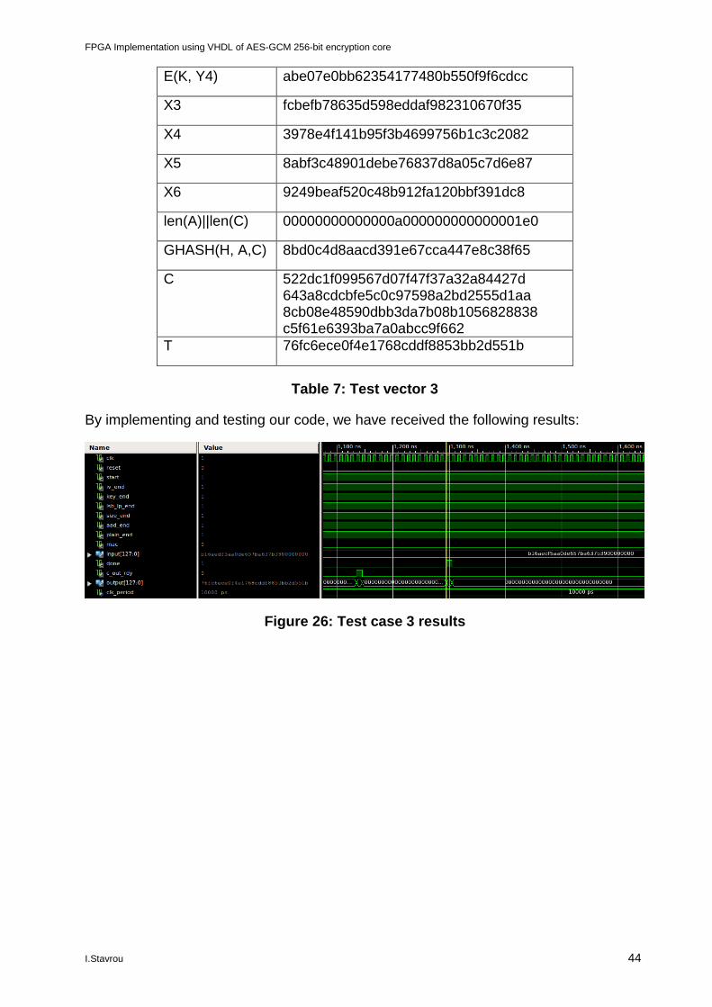
Test vector 3 is presented in table 7 where we have used both AAD and non-zero values.
Variable Value
K feffe9928665731c6d6a8f9467308308 feffe9928665731c6d6a8f9467308308
P d9313225f88406e5a55909c5aff5269a 86a7a9531534f7da2e4c303d8a318a72 1c3c0c95956809532fcf0e2449a6b525 b16aedf5aa0de657ba637b39
AAD feedfacedeadbeeffeedfacedeadbeef abaddad2
IV cafebabefacedbaddecaf888
H acbef20579b4b8ebce889bac8732dad7
Y0 cafebabefacedbaddecaf88800000001
E(K, Y0) fd2caa16a5832e76aa132c1453eeda7e
X1 5165d242c2592c0a6375e2622cf925d2
X2 8efa30ce83298b85fe71abefc0cdd01d
Y1 cafebabefacedbaddecaf88800000002
E(K, Y1) 8b1cf3d561d27be251263e66857164e7
Y2 cafebabefacedbaddecaf88800000003
E(K, Y2) e29d258faad137135bd49280af645bd8
Y3 cafebabefacedbaddecaf88800000004
E(K, Y3) 908c82ddcc65b26e887f85341f243d1d
Y4 cafebabefacedbaddecaf88800000005
FPGA Implementation using VHDL of AES-GCM 256-bit encryption core
I.Stavrou 44
E(K, Y4) abe07e0bb62354177480b550f9f6cdcc
X3 fcbefb78635d598eddaf982310670f35
X4 3978e4f141b95f3b4699756b1c3c2082
X5 8abf3c48901debe76837d8a05c7d6e87
X6 9249beaf520c48b912fa120bbf391dc8
len(A)||len(C) 00000000000000a000000000000001e0
GHASH(H, A,C) 8bd0c4d8aacd391e67cca447e8c38f65
C 522dc1f099567d07f47f37a32a84427d 643a8cdcbfe5c0c97598a2bd2555d1aa 8cb08e48590dbb3da7b08b1056828838 c5f61e6393ba7a0abcc9f662
T 76fc6ece0f4e1768cddf8853bb2d551b
Table 7: Test vector 3
By implementing and testing our code, we have received the following results:
Figure 26: Test case 3 results
FPGA Implementation using VHDL of AES-GCM 256-bit encryption core
I.Stavrou 45
REFERENCES
[1] M. Dworkin, Recommendation for Block Cipher Modes of Operation: Galois/Counter Mode (GCM) and GMAC, NIST Special Publication 800-38D, November 2007; http://nvlpubs.nist.gov/nistpubs/Legacy/SP/nistspecialpublication800-38d.pdf
[2] D. A. McGrew, J. Viega, The Galois/Counter Mode of Operation (GCM), May 31, 2005; http://csrc.nist.gov/groups/ST/toolkit/BCM/documents/proposedmodes/gcm/gcm-spec.pdf
[3] Federal Information Processing Standards Publication 197,ADVANCED ENCRYPTION STANDARD (AES), November 26, 2001; http://csrc.nist.gov/publications/fips/fips197/fips-197.pdf
[4] S. Wang, An Architecture for the AES-GCM Security Standard, Waterloo Canada 2006; https://ece.uwaterloo.ca/~cgebotys/NEW/shengsthesis.pdf
[5] P. Sakellariou, ΥΛΟΠΟΙΗΣΗ ΚΡΥΠΤΟ-ΕΠΕΞΕΡΓΑΣΤΙΚΗΣ ΠΛΑΤΦΟΡΜΑΣ ΓΙΑ ΠΙΣΤΟΠΟΙΗΣΗ ΜΗΝΥΜΑΤΩΝ ΣΤΟ ΠΡΟΤΥΠΟ GALOIS/COUNTER MODE, Πανεπιστήμιο Πάτρων 2009; http://nemertes.lis.upatras.gr/jspui/bitstream/10889/2067/1/Final%20Thesis%20Sakellariou%20Panos.pdf
[6] P. J. Ashenden, The VHDL cook book, 1990 First edition; http://www.ics.uci.edu/~alexv/154/VHDL-Cookbook.pdf
[7] P. J. Ashenden, Digital Design (VHDL) An Embedded Systems Approach Using VHDL, 2007
http://nemertes.lis.upatras.gr/jspui/bitstream/10889/2067/1/Final%20Thesis%20Sakellariou%20Panos.pdf