
THE EFFECT OF SECONDARY PHASES AND BIREFRINGENCE ON VISIBLE LIGHT
1
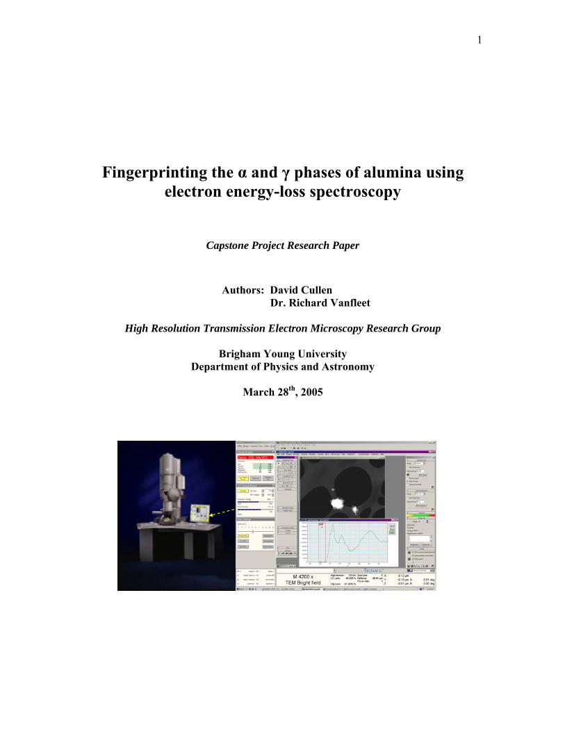
Fingerprinting the α and γ phases of alumina using electron energy-loss spectroscopy
Capstone Project Research Paper
Authors: David Cullen Dr. Richard Vanfleet
High Resolution Transmission Electron Microscopy Research Group
Brigham Young University
Department of Physics and Astronomy
March 28th, 2005

2
Abstract
The alpha and gamma phases of aluminum oxide were fingerprinted using
electron energy-loss spectroscopy (EELS) with an energy resolution of 0.4 eV. Electron
diffraction and powder x-ray diffraction were used to determine the phase of micron and
nanopowder alumina samples. The results from indexing peak and ring diffraction
patterns proved to be ambiguous and were resolved by comparing EELS spectra with
published fingerprints. EELS spectra were generated from the powders with an energy
resolution of 0.4 eV. This energy resolution was achieved using a Tecnai F20 Analytical
Scanning Transmission Electron Microscope (STEM) equipped with a monochromator,
Gatan energy filter (GIF) and high resolution spectrometer in STEM mode. These
fingerprints are compared with published data and discrepancies between the spectra are
discussed. The significance of using a monochromator with STEM mode for
nanoparticle phase identification is addressed, followed by a brief roadmap delineating
the goals of future EELS phase identification research.
Table of Contents
Section Page
Introduction 3
Methods 7
Results 16
Discussion of EELS results 26
Future Research 29
Conclusion 30
Acknowledgements 31
References 32
Appendix 33
3
Introduction
Aluminum oxide (Al2O3) is the most widely used ceramic material and the second
most abundant oxide in the earth’s crust. It has a variety of industrial applications,
especially in the fields of abrasives and wear resistant coatings. Commonly referred to as
alumina, it can be found in seven different forms or phases, each having an identical
stoichiometry, but different crystal structure and hence different mechanical properties.
Six of the seven--chi (χ), eta (η), gamma (γ), kappa (κ), theta (θ), and delta (δ)--are
known as the transition aluminas and form via a thermodynamic transformation sequence
from the alumina hydroxide group.[1] The seventh phase, alpha (α) or corundum, is the
only thermodynamically stable form, and can also be found in the precious gem form as
ruby or sapphire. Most references to aluminum oxide or alumina refer to this seventh
phase.
Because mechanical and crystal properties are phase dependent, certain phases
find greater application in the industrial world. For example, the alpha, kappa, and
gamma phases are widely used as resistant coatings in metal cutting tool applications.[2]
Gamma alumina composite is also used in a special application as a heat insulator in the
support structure of NASA’s Wide-Field Infrared Explorer (WIRE) spacecraft.[3]
Corundum, the most common form of alumina, finds an assortment of everyday
applications ranging from high temperature crucibles to cosmetics. However, the other
phases of alumina have yet to find their application in the industrial world.
Following the current trends of industrial materials research and development,
alumina particle production is moving to the nanoscale. It is clear that efficient phase
4
characterization is an essential precursor to extensive application. As particle size moves
to the nanoscale, contemporary phase characterization techniques are quickly reaching
their limits of resolution. Single nanoparticle phase characterization is an important
companion to advances in nanoparticle production, and can be accomplished using high
resolution transmission electron microscopy (HRTEM). One application of HRTEM
implements a technique called electron-energy loss spectroscopy (EELS).
EELS commands a broad range of applications in materials analysis. In the
specific case of phase identification, the system can be used to generate a phase-
dependent energy-loss spectra which can be used as a type of fingerprint. EELS
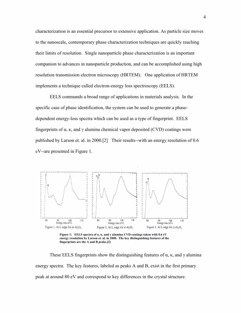
fingerprints of α, κ, and γ alumina chemical vapor deposited (CVD) coatings were
published by Larson et. al. in 2000.[2] Their results--with an energy resolution of 0.6
eV--are presented in Figure 1.
Figure 1: EELS spectra of α, κ, and γ alumina CVD coatings taken with 0.6 eV
energy resolution by Larson et. al. in 2000. The key distinguishing features of the fingerprints are the A and B peaks.[2]
These EELS fingerprints show the distinguishing features of α, κ, and γ alumina
energy spectra. The key features, labeled as peaks A and B, exist in the first primary
peak at around 80 eV and correspond to key differences in the crystal structure.
5
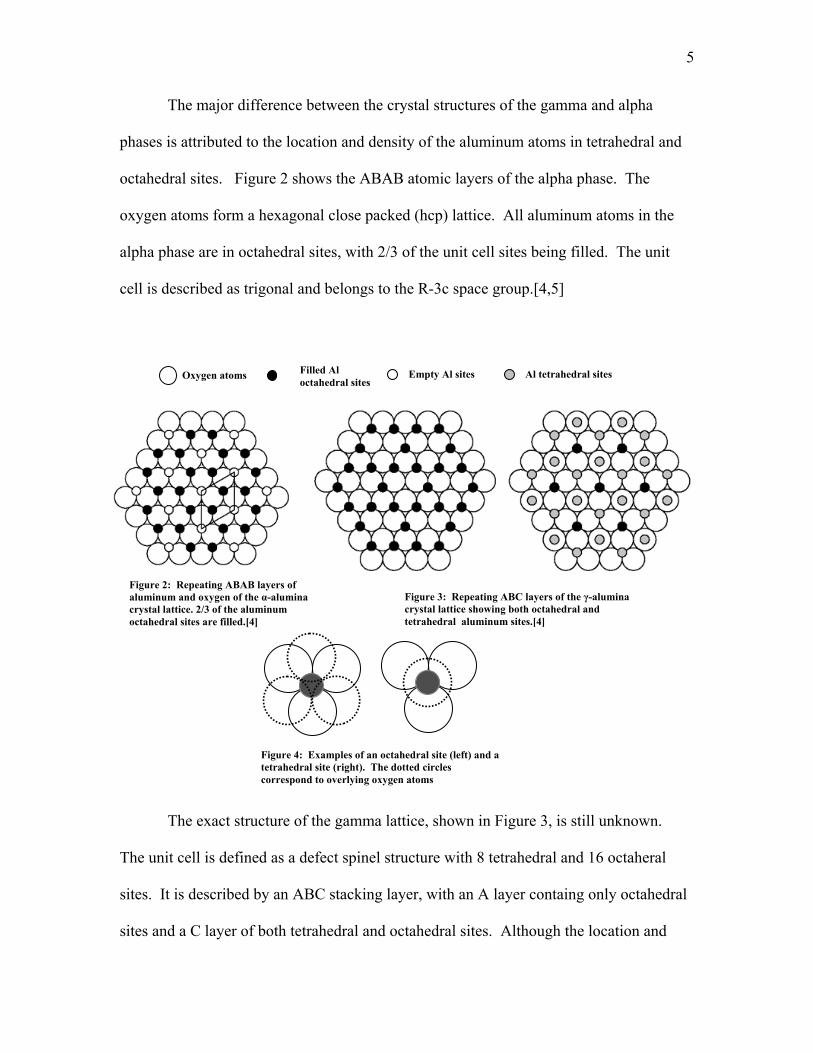
The major difference between the crystal structures of the gamma and alpha
phases is attributed to the location and density of the aluminum atoms in tetrahedral and
octahedral sites. Figure 2 shows the ABAB atomic layers of the alpha phase. The
oxygen atoms form a hexagonal close packed (hcp) lattice. All aluminum atoms in the
alpha phase are in octahedral sites, with 2/3 of the unit cell sites being filled. The unit
cell is described as trigonal and belongs to the R-3c space group.[4,5]
Filled Al octahedral sites
The exact structure of the gamma lattice, shown in Figure 3, is still unknown.
The unit cell is defined as a defect spinel structure with 8 tetrahedral and 16 octaheral
sites. It is described by an ABC stacking layer, with an A layer containg only octahedral
sites and a C layer of both tetrahedral and octahedral sites. Although the location and
Figure 2: Repeating ABAB layers of aluminum and oxygen of the α-alumina crystal lattice. 2/3 of the aluminum octahedral sites are filled.[4]
Figure 3: Repeating ABC layers of the γ-alumina crystal lattice showing both octahedral and tetrahedral aluminum sites.[4]
Figure 4: Examples of an octahedral site (left) and a tetrahedral site (right). The dotted circles correspond to overlying oxygen atoms
Oxygen atoms Empty Al sites Al tetrahedral sites
6
ratio of these sites is still under dispute, most sources agree that that the unit cell is face
centered cubic (fcc) and belongs to the Fd-3m space group.[4,5]
It is suggested that the density of the octahedral and tetrahedral sites determines
the relative locations of the A and B features in the primary peak of the alumina EELS
spectrum.[2] Whatever the case, EELS phase identification rests on our ability to resolve
these special features, which requires an energy resolution of less than 1 eV.
The scope of this project spans three major goals: first, to investigate how
implementing an energy monochromator with EELS can improve energy resolution;
second, to identify new features rising in the spectra at finer energy resolution; and, third,
to demonstrate the capability of using scanning transmission electron microscopy
(STEM) in tandem with the monochromator and EELS system to positively fingerprint
single nanoparticles. As a matter of course, this paper briefly reviews the TEM sample
preparation techniques used for this investigation, including wedge tripod polishing,
dimpling, and powder sample preparation. This is followed by an explanation of electron
diffraction as a tool for the phase identification of the alpha and gamma phases. Results
of this analysis on nanopowders are presented in addition to results from x-ray powder
spectroscopy. Finally, 0.4 eV energy resolution energy-loss spectra of the alpha and
gamma phases of alumina, acquired using a unique HRTEM system which combines a
state-of-the-art electron beam monochromator and EELS system, are presented and
interpreted, followed by a discussion of important future EELS research.
7
Methods
Materials
The principle materials used in this analysis were micron and nanosized powders.
A 60 nanometer γ aluminum oxide powder was purchased from Alfa Aesar, and a coarser
grained, 60 micron γ aluminum oxide called CATALOX SBA-200 was donated by Dr.
Calvin H Bartholomew of the BYU Chemical Engineering Department.
The polycrystalline α-alumina used in scanning electron microscopy (SEM) and
electron diffraction came from an alumina crucible donated by Dr. Jeff Farrer of the BYU
Physics Department.
Equipment and Software
This project utilized many types of equipment and computer software. The
sample preparation stage required a slow speed diamond saw, polishing tripod, diamond
lapping films, polishing wheel, 3mm ultrasonic disc cutter, dimpler, and precision-ion
mill.
The microscopy part of the project utilized two transmission electron
microscopes, a Tecnai F30 TEM and Tecnai F20 Analytical STEM equipped with a
monochromator, GIF, and EELS system. Images and diffraction patterns were recorded
on image plates and read out on a Ditabis laser drum scanner linked to Digital
Micrograph imaging software, which was also used to index the diffraction patterns.
8
EELS spectra from the Tecnai F20 were also recorded and analyzed in Digital
Micrograph. Further, an analysis on the grain size and orientation of the polycrystalline
α-alumina was carried out using a Philips XL30 S-Feg SEM equipped with a
backscattered electron detector.
Sample Preparation
We initially explored to two popular sample preparation techniques for this
analysis. These processes are wedge tripod polishing and dimpling, which will be
described briefly. Since TEM samples must be electron transparent—meaning a
maximum thickness of 100 nanometers--these techniques require liberal quantities of
time and patience. Fortunately, we located two sources of γ-alumina powder, and the
previous techniques could be temporarily substituted for a much quicker process. These
powders, identified in the materials section of this paper, were used for the TEM electron
diffraction, x-ray powder diffraction (XPDS), and EELS investigations.
The first undertaking of this project was a joint effort with BYU student Jason
Neff to produce a set of tripod polishers for the TEM specimen preparation lab.
Computer generated instructions and diagrams of this process were adapted from a set of
handwritten notes and are found in Appendix A. All materials--including aluminum,
glass, Teflon, and micrometers--were provided by Dr. Vanfleet and machining was
carried out in the Crabtree machine shop.
9
Samples for TEM and EELS analysis were initially designed to be wedge-type. A
wedge sample demands many delicate hours of preparation, and, more often than not,
ultimately ends in disaster. However, the product of a successful mechanical polish can
provide an exceptionally thin edge for TEM analysis. The edge allows us to control
thickness and crystal orientation during TEM operations, which are essential to obtaining
clear and accurate diffraction patterns.
Since we were interested in understanding the average grain size and
disorientation angles in the polycrystalline corundum, samples from the crucible were
first prepared for an SEM analysis. Following the literature on OIM sample preparation,
several specimens underwent a series of quick mechanical polishes with 15 micron to 1
micron lapping films and then ten minutes of ion milling.[6,7] Information concerning
crystal size and orientation could then be obtained using an SEM capable of orientation
imaging microscopy (OIM). An analysis of the effect of mechanical polishing on the
specimen surface was also carried out in conjunction
with this analysis.
We confirmed that the material was
polycrystalline with an average grain diameter of
200 microns. We feared that the large grains would rip out of the thin area of the wedge
as we polished, leaving a thick, jagged edge instead of a thin, smooth area for analysis.
For this reason, the wedge technique was temporarily abandoned.
Figure 5: Example of a wedge sample. The tip is polished to be electron transparent (<100 nm).
We next worked towards preparing samples using a dimpling technique. This
began by cutting small sections from the polycrystalline crucible using a low speed
diamond wheel saw. The faces were polished flat using a tripod polisher and 30 micron
10
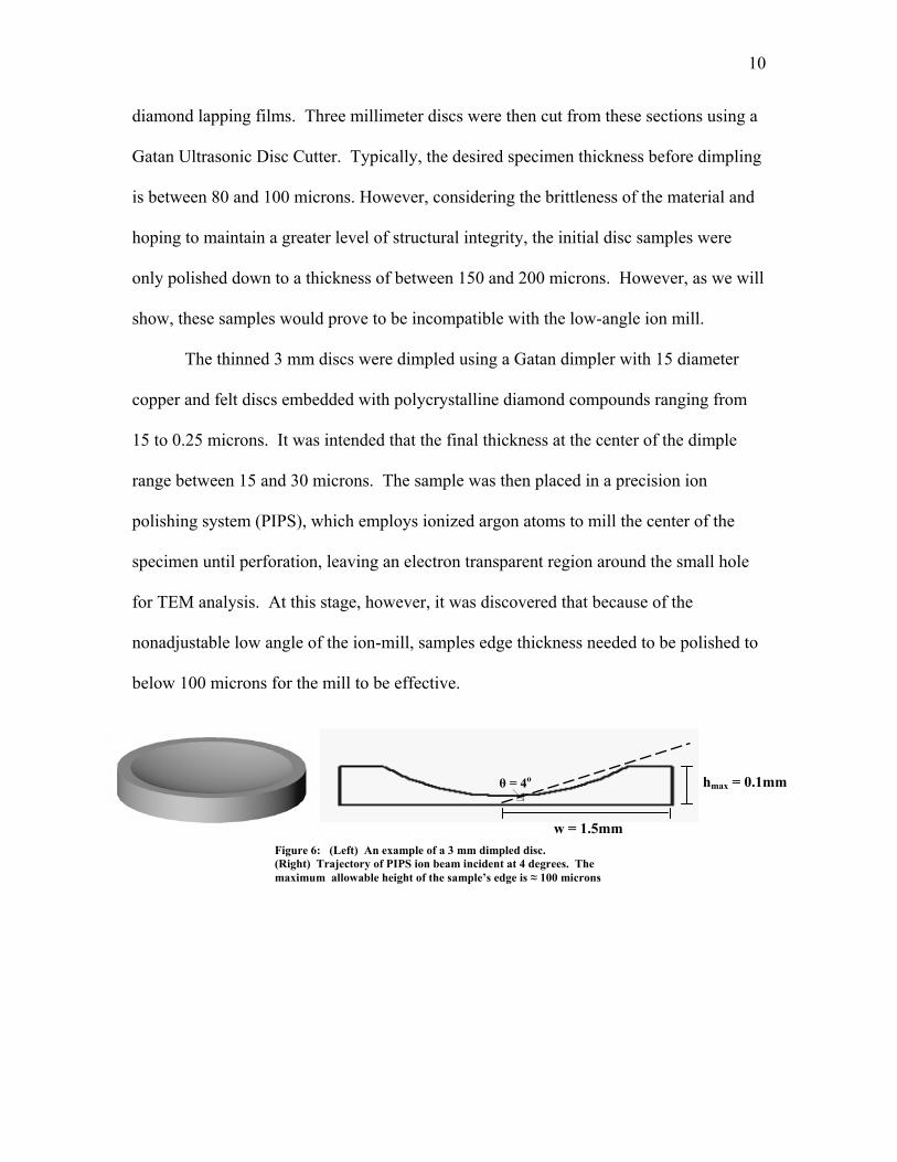
diamond lapping films. Three millimeter discs were then cut from these sections using a
Gatan Ultrasonic Disc Cutter. Typically, the desired specimen thickness before dimpling
is between 80 and 100 microns. However, considering the brittleness of the material and
hoping to maintain a greater level of structural integrity, the initial disc samples were
only polished down to a thickness of between 150 and 200 microns. However, as we will
show, these samples would prove to be incompatible with the low-angle ion mill.
The thinned 3 mm discs were dimpled using a Gatan dimpler with 15 diameter
copper and felt discs embedded with polycrystalline diamond compounds ranging from
15 to 0.25 microns. It was intended that the final thickness at the center of the dimple
range between 15 and 30 microns. The sample was then placed in a precision ion
polishing system (PIPS), which employs ionized argon atoms to mill the center of the
specimen until perforation, leaving an electron transparent region around the small hole
for TEM analysis. At this stage, however, it was discovered that because of the
nonadjustable low angle of the ion-mill, samples edge thickness needed to be polished to
below 100 microns for the mill to be effective.
hmax = 0.1mm θ = 4o
w = 1.5mm Figure 6: (Left) An example of a 3 mm dimpled disc.
(Right) Trajectory of PIPS ion beam incident at 4 degrees. The maximum allowable height of the sample’s edge is ≈ 100 microns
11
Fortunately, we discovered an on-campus source of micron-sized gamma alumina
powder and later were able to purchase nanosized powders of the same phase. Sample
preparation for powders is a very simple process of applying a small quantity of powder
on to a lacy carbon grid.
There are several disadvantages to using powders, however. Powders tend to
clump together, forming sections of varying crystal orientation, thickness, and, as we
would soon discover, composition. Single particle isolation can be very difficult.
Fortunately, these powders proved to be excellent samples. A small amount of powder
was sprinkled on a three millimeter lacy carbon film, which could be immediately
inserted into the microscope for analysis.
Electron Diffraction
Once a sample was prepared for TEM analysis, its phase was confirmed using
electron diffraction. The diffraction mode utilizes the electrons diffracted by the atomic
planes of the crystal. Information concerning atomic spacing and crystal structure can be
harvested from the images by a process called indexing.
Diffraction from a single, uniform crystal forms a series of peaks called a spot
diffraction pattern, while polycrystalline and amorphous materials will scatter electrons
to form continuous rings.
12
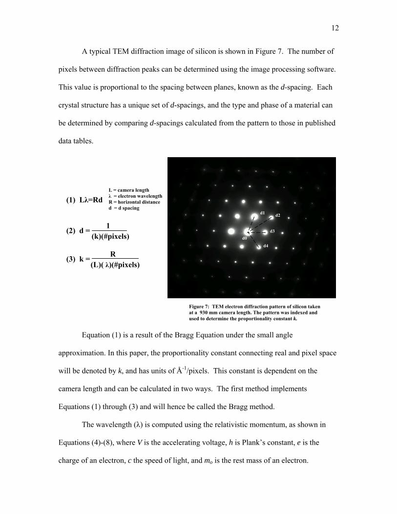
A typical TEM diffraction image of silicon is shown in Figure 7. The number of
pixels between diffraction peaks can be determined using the image processing software.
This value is proportional to the spacing between planes, known as the d-spacing. Each
crystal structure has a unique set of d-spacings, and the type and phase of a material can
be determined by comparing d-spacings calculated from the pattern to those in published
data tables.
L = camera length λ = electron wavelength (1) Lλ=Rd R = horizontal distance d = d spacing
d1
Equation (1) is a result of the Bragg Equation under the small angle
approximation. In this paper, the proportionality constant connecting real and pixel space
will be denoted by k, and has units of Å-1/pixels. This constant is dependent on the
camera length and can be calculated in two ways. The first method implements
Equations (1) through (3) and will hence be called the Bragg method.
The wavelength (λ) is computed using the relativistic momentum, as shown in
Equations (4)-(8), where V is the accelerating voltage, h is Plank’s constant, e is the
charge of an electron, c the speed of light, and mo is the rest mass of an electron.
d0
d2
d3
d4
1
(2) d = (k)(#pixels)
R (3) k = (L)( λ)(#pixels)
Figure 7: TEM electron diffraction pattern of silicon taken at a 930 mm camera length. The pattern was indexed and used to determine the proportionality constant k.
13
(4) E = Eo + U = moc2 + (eV)
(5) E2 = (moc2) 2+ (pc) 2
(E 2 - mo2c 4) 1/2
(6) p = c (eV(eV+2moc2)) 1/2
p = c
2moc2 ] 1/2
[ 2moeV(1+ eV ) p =
(7) λ = h/p
h
The second method for computing the proportionality constant (k) utilizes a direct
comparison of pixel spacing to theoretical d-spacings and hereon will be referred to as the
method of ratios. As an example, silicon is a cubic lattice with a lattice parameter (a) of
5.42 Å.[8] The d-spacings in silicon can be calculated by inserting integer values for the
miller indices (j, k, l) into the d-spacing formula for a cubic lattice, given by Equation (9).
Ratios of these theoretical d-spacings computed from Equation (9) are then
compared to ratios of the pixel spacings. The value of k can then be determined by
multiplying the appropriate theoretical d-spacing with its corresponding value in pixel
space, as shown by Equation (10).
(9) d = a
[ j2+k2+l2 ] 1/2
(8) λ =
[ 2moeV(1+ 2moc2 eV
) ] 1/2 ≈1.968 ρm
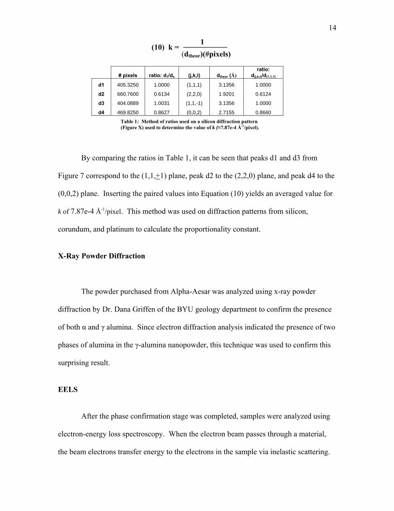
14
(dtheor)(#pixels) (10) k = 1
ratio:
d(j,k,l)/d(1,1,1) dtheor (Å) # pixels ratio: d1/dx (j,k,l)
d1 405.3250 1.0000 (1,1,1) 3.1356 1.0000
d2 660.7600 0.6134 (2,2,0) 1.9201 0.6124
d3 404.0889 1.0031 (1,1,-1) 3.1356 1.0000
d4 469.8250 0.8627 (0,0,2) 2.7155 0.8660 Table 1: Method of ratios used on a silicon diffraction pattern
(Figure X) used to determine the value of k (≈7.87e-4 Å-1/pixel).
By comparing the ratios in Table 1, it can be seen that peaks d1 and d3 from
Figure 7 correspond to the (1,1,+1) plane, peak d2 to the (2,2,0) plane, and peak d4 to the
(0,0,2) plane. Inserting the paired values into Equation (10) yields an averaged value for
k of 7.87e-4 Å-1/pixel. This method was used on diffraction patterns from silicon,
corundum, and platinum to calculate the proportionality constant.
X-Ray Powder Diffraction
The powder purchased from Alpha-Aesar was analyzed using x-ray powder
diffraction by Dr. Dana Griffen of the BYU geology department to confirm the presence
of both α and γ alumina. Since electron diffraction analysis indicated the presence of two
phases of alumina in the γ-alumina nanopowder, this technique was used to confirm this
surprising result.
EELS
After the phase confirmation stage was completed, samples were analyzed using
electron-energy loss spectroscopy. When the electron beam passes through a material,
the beam electrons transfer energy to the electrons in the sample via inelastic scattering.
15
These excited electrons in turn emit that energy in different forms, such as x-rays, auger
electrons, and secondary electrons, which can all be analyzed to extract information about
the specimen. EELS is an analysis of the transmitted beam electrons, and thus is a direct
measurement of the energy transfer to the material. Specifically, we used EELS to
measure the energy lost due to inner shell excitation, or the transfer of energy to the
electrons in the inner shells of the atoms. The number of electrons (counts) detected is
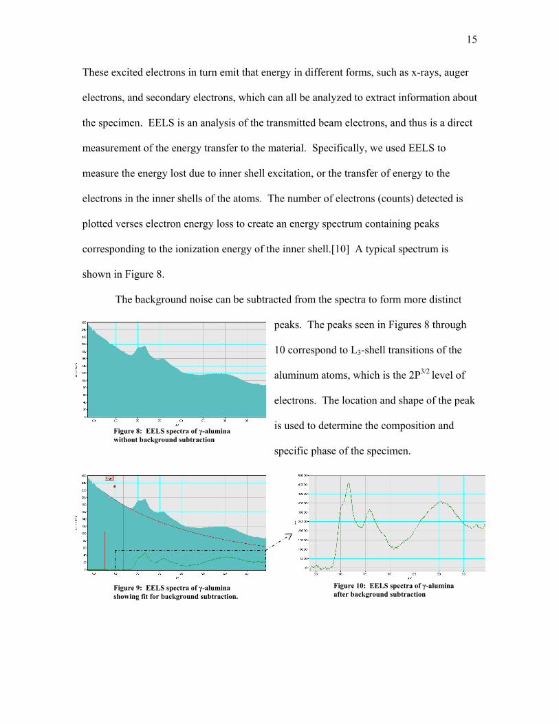
plotted verses electron energy loss to create an energy spectrum containing peaks
corresponding to the ionization energy of the inner shell.[10] A typical spectrum is
shown in Figure 8.
The background noise can be subtracted from the spectra to form more distinct
peaks. The peaks seen in Figures 8 through
10 correspond to L3-shell transitions of the
aluminum atoms, which is the 2P3/2 level of
electrons. The location and shape of the peak
is used to determine the composition and
specific phase of the specimen.
Figure 8: EELS spectra of γ-alumina without background subtraction
Figure 10: EELS spectra of γ-alumina after background subtraction
Figure 9: EELS spectra of γ-alumina showing fit for background subtraction.
16
The energy resolution is determined by taking the full width at half maximum
(FWHM) of the zero loss peak. The eV axis can be calibrated by setting the center of the
zero loss to 0 eV, but because the axis of the spectrum is continuously shifting during
analysis, we also took spectra of the carbon grid to determine the offset of the alumina
spectra. We expect the edge of the gamma and alpha alumina spectra to fall at about
78 eV.[10]
Results
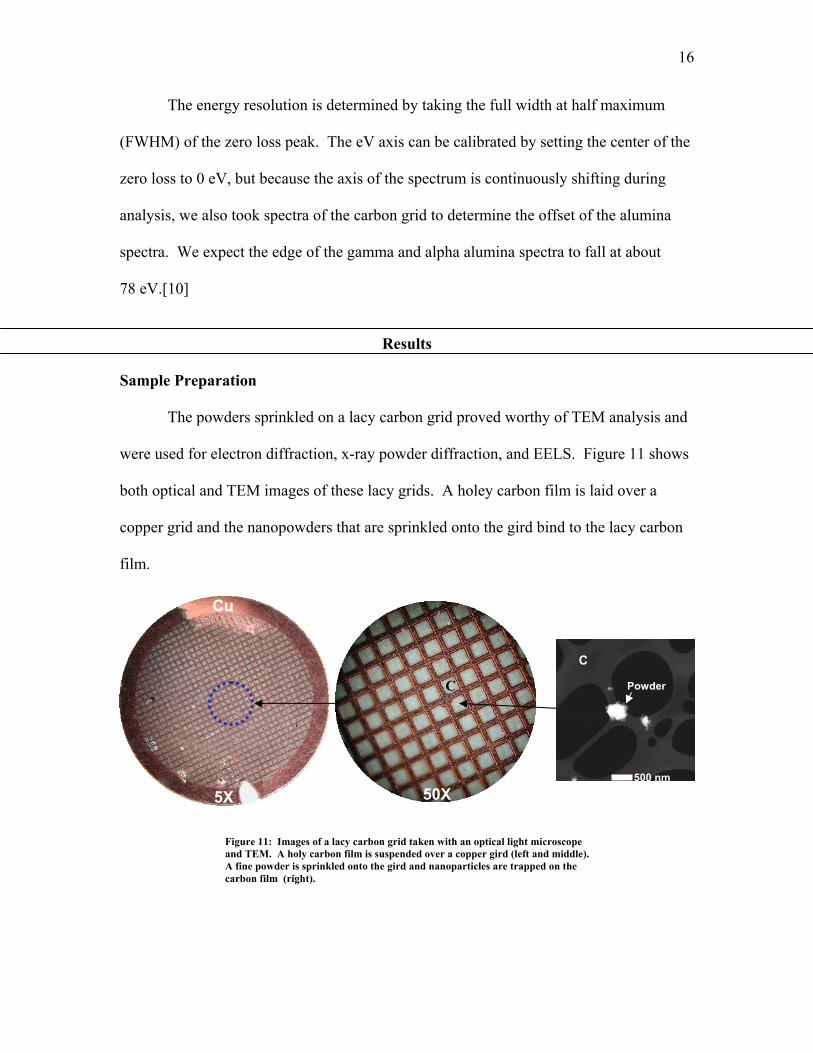
Sample Preparation
The powders sprinkled on a lacy carbon grid proved worthy of TEM analysis and
were used for electron diffraction, x-ray powder diffraction, and EELS. Figure 11 shows
both optical and TEM images of these lacy grids. A holey carbon film is laid over a
copper grid and the nanopowders that are sprinkled onto the gird bind to the lacy carbon
film.
50X 500 nm
Cu
5X
Powder
C
C
Figure 11: Images of a lacy carbon grid taken with an optical light microscope and TEM. A holy carbon film is suspended over a copper gird (left and middle). A fine powder is sprinkled onto the gird and nanoparticles are trapped on the carbon film (right).
17
A wedge sample of alpha alumina was also used in the initial stages of the project
as a standard to determine the proportionality factor k. As previously stated, it was
determined that before dimpling and ion-milling, 3mm discs need to be polished to a
thickness of less than 100 microns.
5X
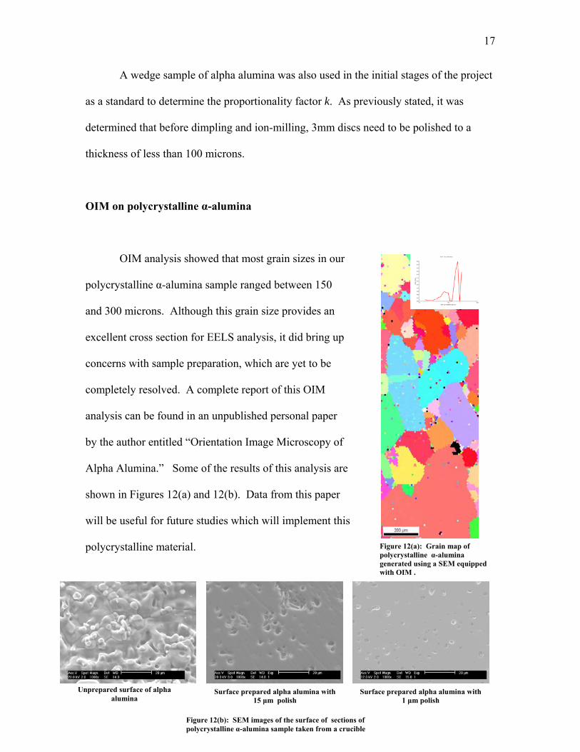
OIM on polycrystalline α-alumina
OIM analysis showed that most grain sizes in our
polycrystalline α-alumina sample ranged between 150
and 300 microns. Although this grain size provides an
excellent cross section for EELS analysis, it did bring up
concerns with sample preparation, which are yet to be
completely resolved. A complete report of this OIM
analysis can be found in an unpublished personal paper
by the author entitled “Orientation Image Microscopy of
Alpha Alumina.” Some of the results of this analysis are
shown in Figures 12(a) and 12(b). Data from this paper
will be useful for future studies which will implement t
polycrystalline material.
5X
his
Figure 12(a): Grain map of polycrystalline α-alumina generated using a SEM equipped with OIM .
Unprepared surface of alpha alumina
Surface prepared alpha alumina with 15 μm polish
Surface prepared alpha alumina with 1 μm polish
Figure 12(b): SEM images of the surface of sections of polycrystalline α-alumina sample taken from a crucible
18
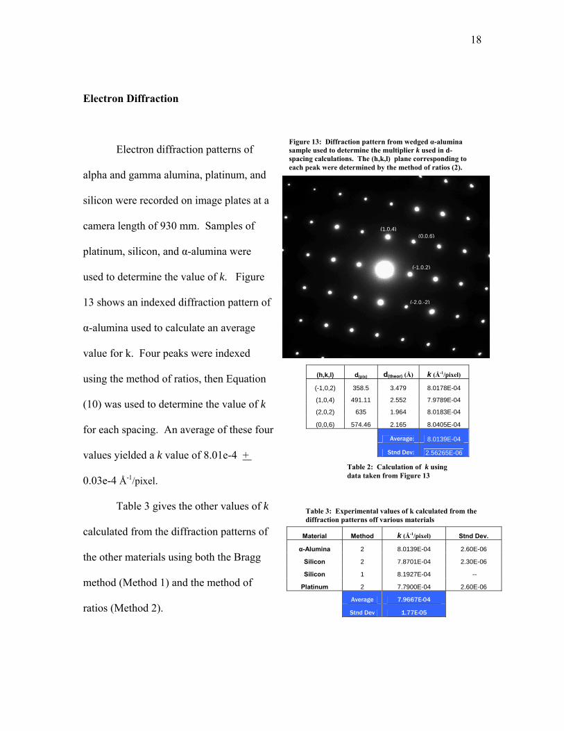
Electron Diffraction
Electron diffraction patterns of
alpha and gamma alumina, platinum, and
silicon were recorded on image plates at a
camera length of 930 mm. Samples of
platinum, silicon, and α-alumina were
used to determine the value of k. Figure
13 shows an indexed diffraction pattern of
α-alumina used to calculate an average
value for k. Four peaks were indexed
using the method of ratios, then Equation
(10) was used to determine the value of k
for each spacing. An average of these four
values yielded a k value of 8.01e-4 +
0.03e-4 Å-1/pixel.
(
(1,0,4) (0,0,6)
-1,0,2)
(-2,0,-2)
d(theor) (Å) k (Å-1/pixel) (h,k,l) d(pix)
(-1,0,2) 358.5 3.479 8.0178E-04
(1,0,4) 491.11 2.552 7.9789E-04
(2,0,2) 635 1.964 8.0183E-04
(0,0,6) 574.46 2.165 8.0405E-04
Average: 8.0139E-04
Stnd Dev: 2.56265E-06
Figure 13: Diffraction pattern from wedged α-alumina sample used to determine the multiplier k used in d-spacing calculations. The (h,k,l) plane corresponding to each peak were determined by the method of ratios (2).
Table 2: Calculation of k using data taken from Figure 13
Table 3 gives the other values of k
calculated from the diffraction patterns of
the other materials using both the Bragg
method (Method 1) and the method of
ratios (Method 2).
Material Method k (Å-1/pixel) Stnd Dev.
α-Alumina 2 8.0139E-04 2.60E-06
Silicon 2 7.8701E-04 2.30E-06
Silicon 1 8.1927E-04 --
Platinum 2 7.7900E-04 2.60E-06
Average 7.9667E-04
Stnd Dev 1.77E-05
Table 3: Experimental values of k calculated from the diffraction patterns off various materials
19
As seen in Table 3, the average value of k calculated from these different
materials is 8.0e-4 + .2e-4 Å-1/pixel. This value was used to determine the d-spacings in
later diffraction patterns to a rather remarkable degree of accuracy.
From Equations (1)-(3), we note that the proportionality constant is a function of
camera length. Using the platinum standard, nine diffraction patterns were taken at
camera lengths from 0.190 m to 1.9 m. The values of k calculated from these patterns
were plotted against working distance to get Equation (12) with an R2 value of 0.997.
Figure 14 shows a plot of this fit along side the theoretical curve derived from Equation
(3). These equations can be used to determine an approximate value of k for any working
distance.
∆k (Å-1/pixel)
Working Distance (mm)
Multiplier k (Å-1/pixel)
Working Distance L (mm)
(11) ktheor= αR(Lλ)-1
(12) kexp = .8496*L-1.0226 Figure 14: Comparison of theoretical and experimental curves for determining the proportionally constant used in relating distance in image-space (pixels) of diffraction patterns recorded on image plates and real space (Å). The experimental curve resulted from a fit to 9 different working dusing diffraction from a platinum crystal. Values for k were computed using Method 2 . Platinum has an fcc lattice, and theoretical d-spacings can be easily calculated using equation where a=3.9321 Å. ktheor (11) is a result of eq. (1)-(3),where α=1e-7, R=14.5, λ=1.968 ρm.
istances
20
Also displayed in Figure 14 is a plot of the difference between ktheor and kexp. As
camera length increases, the two curves begin to diverge. The maximum difference
between the curves is about 1.2e-05 Å-1/pixel at a camera length near 1.5 m. This is
roughly a 2% difference, which, for most calculations, is an acceptable degree of error.
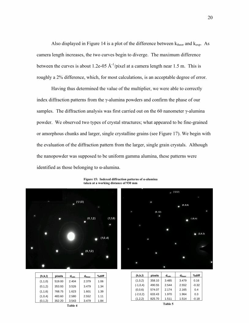
Having thus determined the value of the multiplier, we were able to correctly
index diffraction patterns from the γ-alumina powders and confirm the phase of our
samples. The diffraction analysis was first carried out on the 60 nanometer γ-alumina
powder. We observed two types of crystal structures; what appeared to be fine-grained
or amorphous chunks and larger, single crystalline grains (see Figure 17). We begin with
the evaluation of the diffraction pattern from the larger, single grain crystals. Although
the nanopowder was supposed to be uniform gamma alumina, these patterns were
identified as those belonging to α-alumina.
Figure 15: Indexed diffraction patterns of α-alumina taken at a working distance of 930 mm
(h,k,l) pixels dcalc dtheor %diff
(1,1,0) 519.00 2.404 2.379 1.06
(0,1,2) 353.93 3.526 3.479 1.34
(1,1,6) 768.75 1.623 1.601 1.39
(1,0,4) 483.60 2.580 2.552 1.11 (0,1,2) 352.20 3.543 3.479 1.84
(h,k,l) pixels dcalc dtheor %diff
(1,0,2) 358.10 3.485 3.479 0.16 (-1,0,4) 490.55 2.544 2.552 -0.32 (0,0,6) 574.07 2.174 2.165 0.4 (-2,0,2) 633.43 1.970 1.964 0.3 (1,2,2) 825.70 1.511 1.514 -0.18
Table 5 Table 4
21
Figure 15 shows two such diffraction patterns with the accompanying diffraction
data co
ut to be agglomerated chunks of
gamma
ese
ntained in Tables 4 and 5. The column labeled [%diff] gives the percent
difference between the measured and theoretical values.
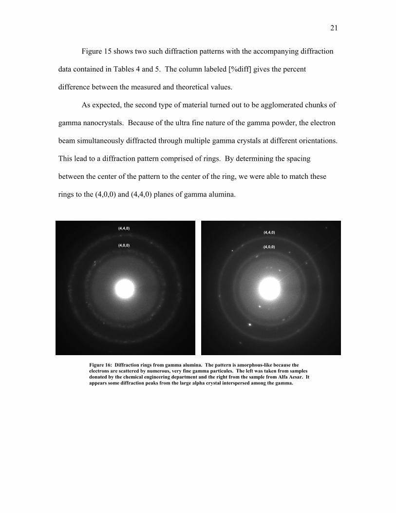
As expected, the second type of material turned o
nanocrystals. Because of the ultra fine nature of the gamma powder, the electron
beam simultaneously diffracted through multiple gamma crystals at different orientations.
This lead to a diffraction pattern comprised of rings. By determining the spacing
between the center of the pattern to the center of the ring, we were able to match th
rings to the (4,0,0) and (4,4,0) planes of gamma alumina.
(4,4,0) (4,4,0)
(4,0,0) (4,0,0)
Figure 16: Diffraction rings from gamma alumina. The pattern is amorphous-like because the electrons are scattered by numerous, very fine gamma particules. The left was taken from samples donated by the chemical engineering department and the right from the sample from Alfa Aesar. It appears some diffraction peaks from the large alpha crystal interspersed among the gamma.
22
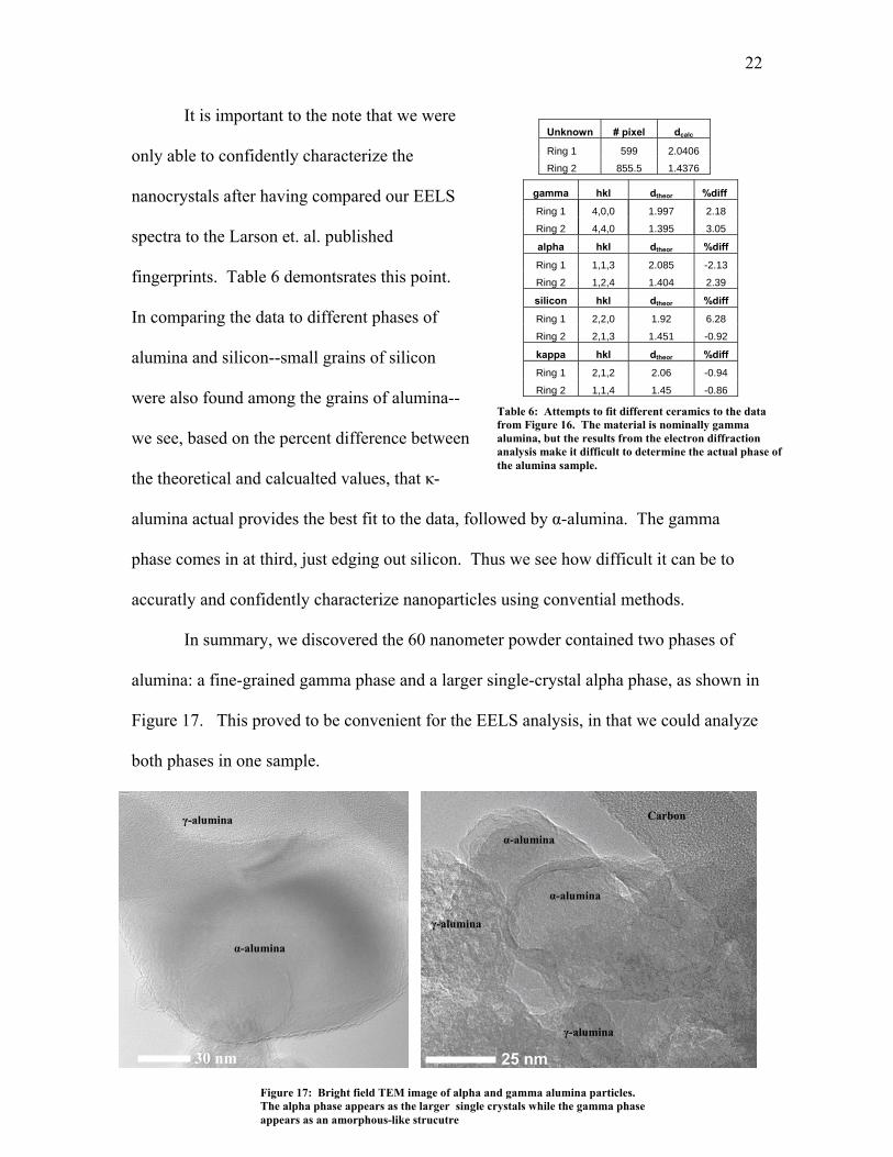
It is important to the note that we were
only able to confidently characterize the
nanocrystals after having compared our EELS
spectra to the Larson et. al. published
fingerprints. Table 6 demontsrates this point.
In comparing the data to different phases of
alumina and silicon--small grains of silicon
were also found among the grains of alumina--
we see, based on the percent difference between
the theoretical and calcualted values, that κ-
alumina actual provides the best fit to the data, followed by α-alumina. The gamma
phase comes in at third, just edging out silicon. Thus we see how difficult it can be to
accuratly and confidently characterize nanoparticles using convential methods.
Unknown # pixel dcalc
Ring 1 599 2.0406
In summary, we discovered the 60 nanometer powder contained two phases of
alumina: a fine-grained gamma phase and a larger single-crystal alpha phase, as shown in
Figure 17. This proved to be convenient for the EELS analysis, in that we could analyze
both phases in one sample.
gamma
Ring 2 855.5 1.4376
hkl dtheor %diff
Ring 1 4,0,0 1.997 2.18
Ring 2 4,4,0 1.395 3.05
alpha hkl dtheor %diff
Ring 1 1,1,3 2.085 -2.13
Ring 2 1,2,4 1.404 2.39
silicon hkl dtheor %diff
Ring 1 2,2,0 1.92 6.28
Ring 2 2,1,3 1.451 -0.92
kappa hkl dtheor %diff
Ring 1 2,1,2 2.06 -0.94
Ring 2 1,1,4 1.45 -0.86 Table 6: Attempts to fit different ceramics to the data
from Figure 16. The material is nominally gamma alumina, but the results from the electron diffraction analysis make it difficult to determine the actual phase of the alumina sample.
25 nm
Figure 17: Bright field TEM image of alpha and gamma alumina particles. The alpha phase appears as the larger single crystals while the gamma phase appears as an amorphous-like strucutre
α-alumina
30 nm 25 nm
γ-alumina
α-alumina
Carbon
γ-alumina
γ-alumina
α-alumina
23
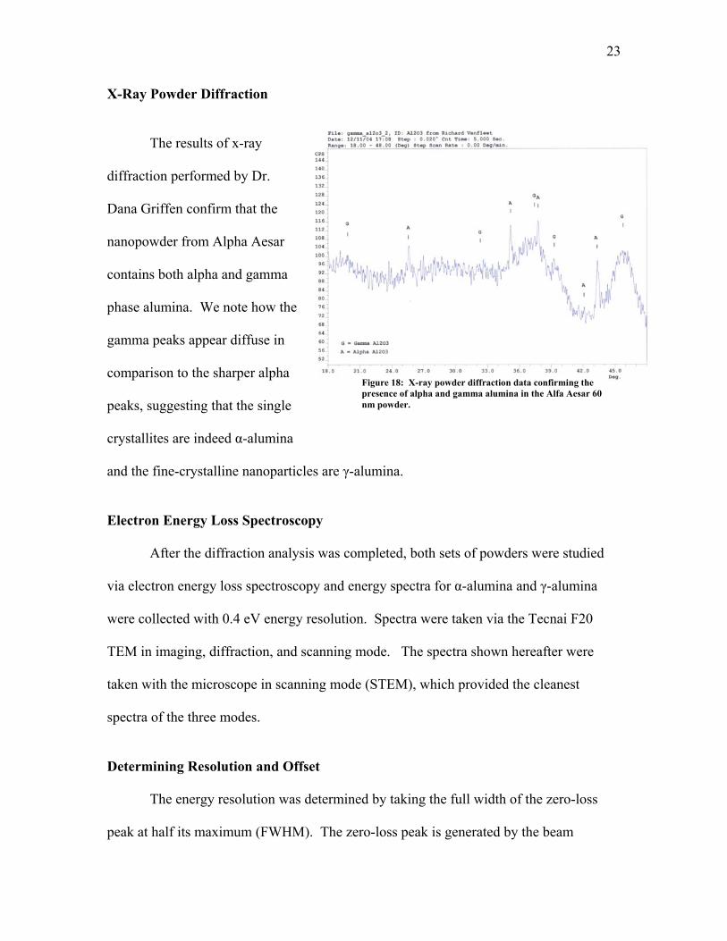
X-Ray Powder Diffraction
The results of x-ray
diffract
les are γ-alumina.
Electron Energy Loss Spectroscopy
s completed, both sets of powders were studied
via elec
Determining Resolution and Offset
rmined by taking the full width of the zero-loss
peak at half its maximum (FWHM). The zero-loss peak is generated by the beam
Figure 18: X-ray powder diffraction data confirming the presence of alpha and gamma alumina in the Alfa Aesar 60 nm powder.
ion performed by Dr.
Dana Griffen confirm that the
nanopowder from Alpha Aesar
contains both alpha and gamma
phase alumina. We note how the
gamma peaks appear diffuse in
comparison to the sharper alpha
peaks, suggesting that the single
crystallites are indeed α-alumina
and the fine-crystalline nanopartic
After the diffraction analysis wa
tron energy loss spectroscopy and energy spectra for α-alumina and γ-alumina
were collected with 0.4 eV energy resolution. Spectra were taken via the Tecnai F20
TEM in imaging, diffraction, and scanning mode. The spectra shown hereafter were
taken with the microscope in scanning mode (STEM), which provided the cleanest
spectra of the three modes.
The energy resolution was dete
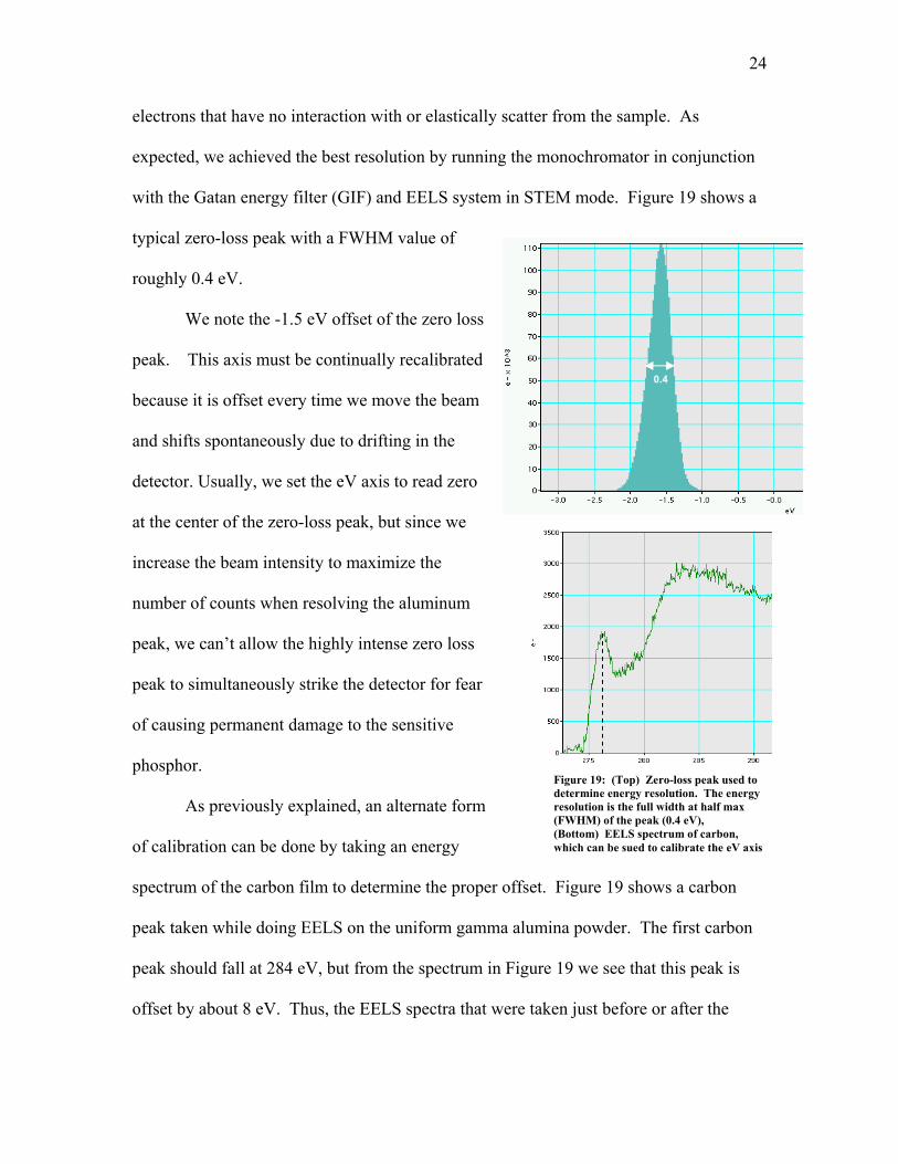
24
electron
ction
hows a
ss
ust be continually recalibrated
because
oss
r
rm
n can be done by taking an energy
spectru
mma alumina powder. The first carbon
s that have no interaction with or elastically scatter from the sample. As
expected, we achieved the best resolution by running the monochromator in conjun
with the Gatan energy filter (GIF) and EELS system in STEM mode. Figure 19 s
typical zero-loss peak with a FWHM value of
roughly 0.4 eV.
We note the -1.5 eV offset of the zero lo
peak. This axis m0.4
it is offset every time we move the beam
and shifts spontaneously due to drifting in the
detector. Usually, we set the eV axis to read zero
at the center of the zero-loss peak, but since we
increase the beam intensity to maximize the
number of counts when resolving the aluminum
peak, we can’t allow the highly intense zero l
peak to simultaneously strike the detector for fea
of causing permanent damage to the sensitive
phosphor.
As previously explained, an alternate fo
of calibratio
Figure 19: (Top) Zero-loss peak used to determine energy resolution. The energy resolution is the full width at half max (FWHM) of the peak (0.4 eV), (Bottom) EELS spectrum of carbon, which can be sued to calibrate the eV axis
m of the carbon film to determine the proper
peak taken while doing EELS on the uniform ga
peak should fall at 284 eV, but from the spectrum in Figure 19 we see that this peak is
offset by about 8 eV. Thus, the EELS spectra that were taken just before or after the
offset. Figure 19 shows a carbon
25
carbon peak was resolved would be offset by roughly that value. However, we did not
to the trouble of constantly calibrating the eV axis since the principle objective of this
investigation was to resolve the features in the primary aluminum peak.
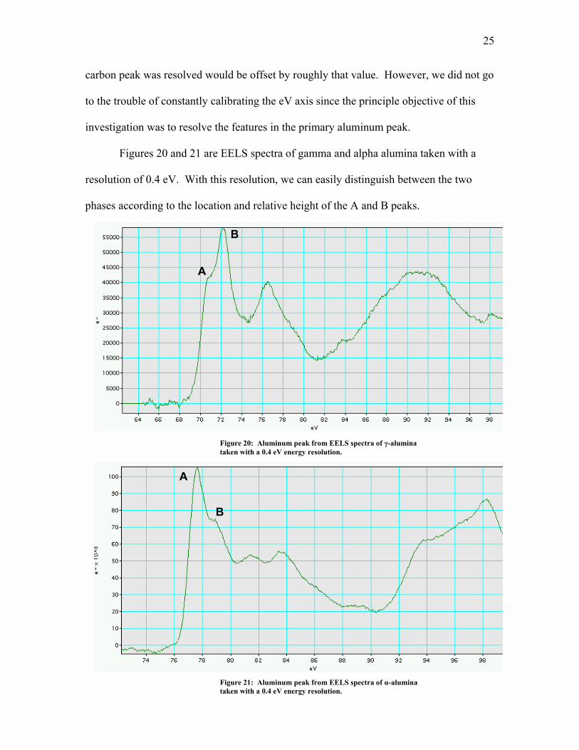
Figures 20 and 21 are EELS spectra of gamma and alpha alumina taken with a
resolution of 0.4 eV. With this resolution, we can easily distinguish betw
go
een the two
phases
according to the location and relative height of the A and B peaks.
A
B
Figure 20: Aluminum peak from EELS spectra of γ-alumina
taken with a 0.4 eV energy resolution.
B
A
Figure 21: Aluminum peak from EELS spectra of α-alumina taken with a 0.4 eV energy resolution.
26
Discussion of EELS Results
The results from the el he difficulty in using this
method to determine the phase of nanosized crystals. Not only were some of the results
inconcl
phase
e our
.
n
ing
/monochromater system in STEM mode to characterize nanoparticles.
Althou
lieve
ectron diffraction study show t
usive, but also very time consuming to process. Although x-ray powder
diffraction results confirmed the presence of α-alumina and γ-alumina, we had no way of
using the data to determine which phase was tied to which strucutre. The ease of
identification by generating and comparing our EELS spectra to the published
fingerprints shows the utility and efficiency of this method. Results came relatively
quickly and were easy to interpret. Only EELS was able to unequivocably prov
suspicions that the fine powder was indeed γ-alumina and the single crystals were α-
alumina. However, the published fingerprints were necessary to make this distinction
Hence, the contemorary techniques of electron diffraction and x-ray powder diffractio
will continue to serve as a necessary part of futurer alumina phase studies. The previous
discussion on electron diffraction should be used to facilitate future characterzation
studies.
The spectra shown in Figures 20 and 21 demonstrate the functionality of runn
the EELS
gh the increased resolution did not reveal any new features in the spectra, we were
able to beautifully resolve the A and B features in the first peak. Although we be
that we can better the energy resolution to 0.2 eV, we don’t expect to see any new, finer
features by increasing energy resolution by another 0.2 eV, as we did in this study.
27
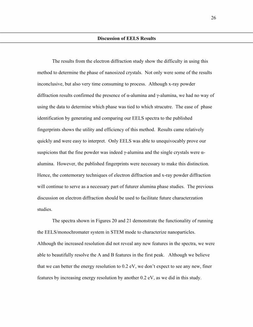
Figures 22 and 23 compare our results with the published fingerprints. The two
α-alumina spectra agree very well until the transition from the second to third region.
Here the general shape of the curve is conserved, but the relative height of the peaks
begins
ere
owever,
e far
ess and attibutes to much of the background.
n lo
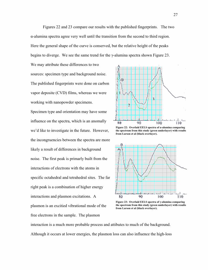
to diverge. We see the same trend for the γ-alumina spectra shown Figure 23.
We may attribute these differences to two
sources: specimen type and background noise.
The published fingerprints were done on carbon
Figure 22: Overlaid EELS spectra of α-alumina comparing the spectrum from this study (green underlayer) with results from Larson et al (black overlayer).
vapor deposite (CVD) films, whereas we w
working with nanopowder specimens.
Specimen type and orientation may have some
influence on the spectra, which is an anomally
we’d like to investigate in the future. H
the incongruencies between the spectra are more
likely a result of differences in background
noise. The first peak is primarly built from the
interactions of electrons with the atoms in
specific octahedral and tetrahedral sites. Th
right peak is a combination of higher energy
interactions and plasmon excitations. A
plasmon is an excitied vibrational mode of the
free electrons in the sample. The plasmon
interaction is a much more probable proc
Although it occurs at lower energies, the plasmo
13
2
Figure 23: Overlaid EELS spectra of γ-alumina comparing the spectrum from this study (green underlayer) with results from Larson et al (black overlayer).
ss can also influence the high-loss
28
end of the spectra if an electron is scattered multiple times. That is to say, the electron
might first excite an aluminum atom then interact with the free electrons in the sam
before exiting the specimen. Such a double-loss electron will contribute to the third
region of the EELS spectra. As sample thickness increases, so do the number of plasm
interactions, causing a taller peak in the third region. Hence, we might conclude that the
thin films used by Larson et al were thicker than the edges of the powders we were
analyzing. Or, on the other hand, the difference may arise simply because of the fit us
to subtract the background from the spectrum. All in all, the differences in the relative
height of the first peak to the third may arise from something as simple as the type and
thickness of the specimen or the fit used for the background subtraction.
We also note a difference in the relative height of the A feature in the two gamma
spectrum (Figure 23). The relative location of the A and B peaks is speculated to be a
function of the octahedral
ple
on
ed
and tetrahedral sites. Thus, the small discrepency in Figure 23
is prob
k
pect of the spectra
since th
ably a function of the material. Observing that the A peak for our gamma spectra
is lower in comparision to the spectra from the CVD films, we suggest that, due to high
surface content or orientatinl differences, the electron interaction with the sites producing
peak B are more preffered in our material. However, without further research into the
matter, we can do little more than speculate.
Again, we note that the peaks of our spectra in Figures 20 and 21 do not fall on
the same energies as published data. This axis can be calibrated using the zero-loss pea
or a carbon peak. However, we were not too concerned with this as
e scope of this study was more concerned with resolving the A and B features of
the first peak.
29
Future Research
Not onl
have o ld be made to master the nuances
of the m chromator/EELS system and push forward the limits of energy resolution. A
proposa
very
ss his high-temperature tube furnace, efforts can be made to
produc
and
we very content with the results of the investigation, but we feel we
have opened the door for further res ld be made to master the nuances
of the m chromator/EELS system and push forward the limits of energy resolution. A
proposa
very
ss his high-temperature tube furnace, efforts can be made to
produc
and
y are we very content with the results of the investigation, but we feel we
pened the door for further research. Efforts shouearch. Efforts shou
onoono
l was written by Dr. Vanfleet for grant money to fund a project using the
polycrystalline material to explore the effect of crystal orientation on the energy spectra.
With much of the work towards mastering sample preparation and understanding the
crystal size and orientation of the material already accomplished, this project could
quickly produce results.
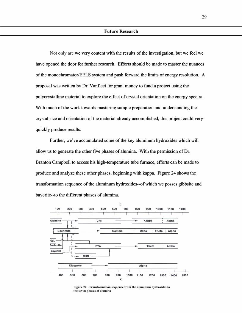
Further, we’ve accumulated some of the key aluminum hydroxides which will
allow us to generate the other five phases of alumina. With the permission of Dr.
Branton Campbell to acce
l was written by Dr. Vanfleet for grant money to fund a project using the
polycrystalline material to explore the effect of crystal orientation on the energy spectra.
With much of the work towards mastering sample preparation and understanding the
crystal size and orientation of the material already accomplished, this project could
quickly produce results.
Further, we’ve accumulated some of the key aluminum hydroxides which will
allow us to generate the other five phases of alumina. With the permission of Dr.
Branton Campbell to acce
e and analyze these other phases, beginning with kappa. Figure 24 shows the
transformation sequence of the aluminum hydroxides--of which we posses gibbsite
bayerite--to the different phases of alumina.
e and analyze these other phases, beginning with kappa. Figure 24 shows the
transformation sequence of the aluminum hydroxides--of which we posses gibbsite
bayerite--to the different phases of alumina.
Figure 24: Transformation sequence from the aluminum hydroxides to the seven phases of alumina
30
Conclusion
We have succeeded in fingerprinting th
e gamma and alpha phases of alumina with
n energy resolution of 0.4 eV. This was done by using a scanning transmission electron
icroscope with electron energy-loss spectroscopy and a monochromator. The analysis
id not reveal any new features in the EELS spectra, but we were able to demonstrate the
anoparticles. While electron diffraction and x-ray powder diffraction can be used for
phase identification, their results weren’t as robust or conclusive as the EELS
fingerprints. This exercise opens the door to future EELS research at BYU, including
investigations of other alumina phases and the effect of crystal orientation on EELS
spectra.
a
m
d
capability of using STEM mode to enhance definition and characterize alumina
n
31
Acknowledgements
The author would like to thank his research advisor and head of the High
Resolution Transmission Electron Microscopy (HRTEM) Research Group, Dr. Vanfleet,
for this research opportunity, help with funding, and constant support. Also, thanks to
Dr. Jeffery Farrer, BYU’s TEM lab manager, for training on microscope operations and
sample preparation, as well as don appreciated was the feedback
given by Dr. Branton Campbell, the faculty capstone advisor.
his
Research and Creative
Activit
ating literature. Also
A special thanks goes to the collaboratory efforts of Dr. Danna Griffin and
XPD machine and Dr. Bartholomew of the Chemical Engineering department for
donating powder samples for this analysis.
The author also acknowledges Alcoa Labs, Alfa Aesar, and Nabaltec for making
available materials and literature for this project.
Finally, sincere appreciation goes to the BYU Office of
y (ORCA) scholarship program, the Mentoring Environmental Grant (MEG)
program, and the BYU Physics department for funding this project.
32
References
] Wefers, K & Misra, C. (1987) Oxides and Hydroxides of Aluminum [1 , Alcoa
Laboratories
[2] Larsson, A., Xackrisson, J., Halvarsson, M. & Ruppi, S. (2000) EELS investigation
of CVD : α-Al2O3, κ-Al2O3, and γ- Al2O3 coatings.
] “New Technology in the WIRE Mission” Retrieved from the World Wide wWb on
January 25, 2005 from: http://sunland.gsfc.nasa.gov/smex/wire/mission/technology.html
[4] Images retrieved from the World Wide Web on March 12, 2005 from: fy.chalmers.se/~ruberto/lic.pdf
] Farrrtz, M. Kumar
299
[8] Ca
[3
[5] Levin, I. & Brandon, D. (1998) Metastable Alumina Polymorphs: Crystal Transition Sequences. J. Am. Ceram. Soc., Vol. 81 No. 8, pp Structures and
1995-2012
[6] Mu ., (1998) Orientation lvihill, M.L., Gulgun, M.A., Bischoff, E., and Ruhle, MImaging Microscopy of Alpha Alumina: Sample Preparation and Texture Analysis, Zeitschrift fur Metallkunde, 89:546
[7 er, J.K, Michael, J.R., and Carter, C.B. (2000), EBSD of Ceramic Materials,
Electron Backscatter Diffraction in Materials Science, A.J. Schwar Academic/Plenum Publishers, New York, N.Y., and B.L. Adams, eds., Klewe
rter, C.B. & Williams, D.B. (1996) Transmission Electron Microscopy. PlenuPress, New Y
m ork, pg 150
[9] Stokes, H.T. (2000). Solid State Physics for Advanced Undergraduate Students.
0] Ahn, C.C. and Krivanek O.L. (Jan 1983) EELS Atlas, A reference guide of electron
[11] St
e Interdépartemental de Microscopie Electronique. Retrieved from the orld Wide Web from: http://cimesg1.epfl.ch/CIOL/ems.html
Brigham Young University, Third Edition
[1energy loss spectra covering all stable elements
adelmann, Pierre (1998). EMS Online: Electron Microscopy Image Simulation. CentrW
[12] Hansen, P.L., Brydson, R., McComb, D.W., & Richardson, I. (1994) EELS
fingerprint of Al-coordination in silicates.
[13] Eg pectroscopy in the Electron
erton, R.F. (1996) Electron Energy-Loss S Microscope. Plenum Press, New York
33
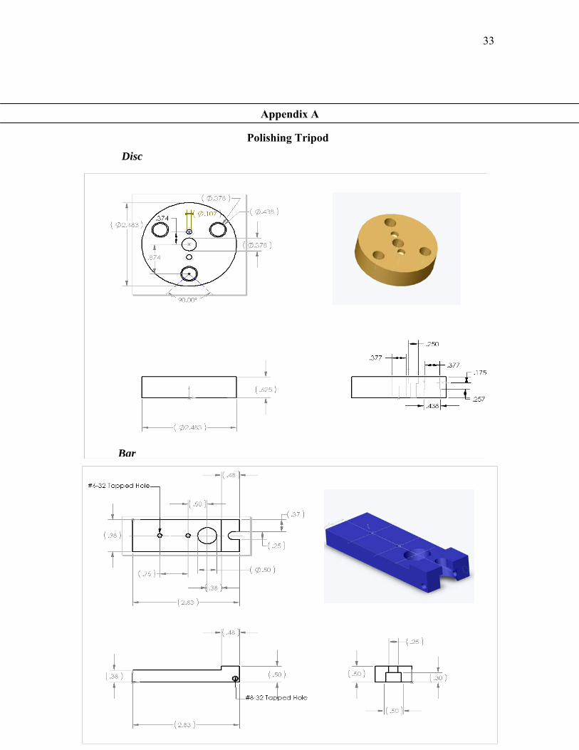
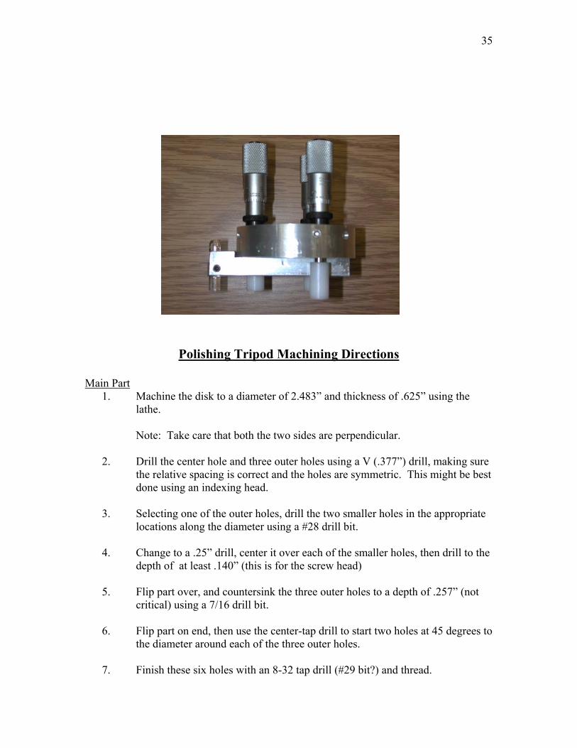
Appendix A
Polishing Tripod
Disc
Bar
34
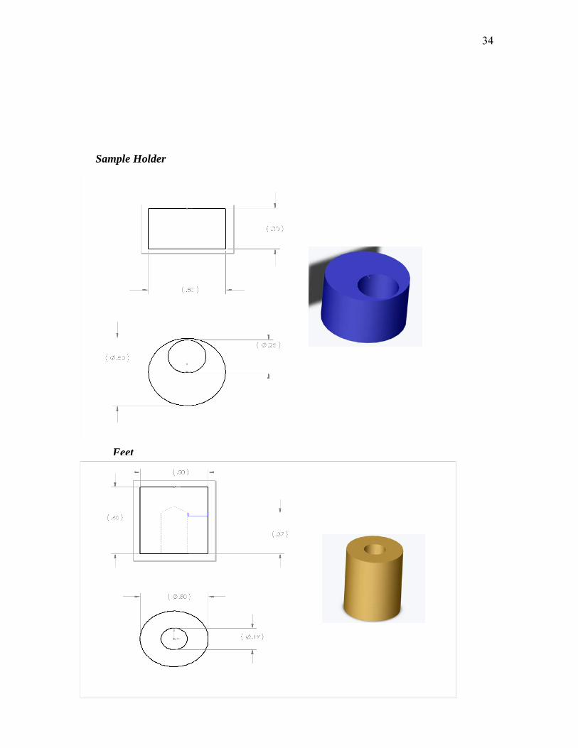
Sample Holder
Feet
35
Polishing Tripod Machining Directions
Main Part 1. Machine the disk to a diameter of 2.483” and thickness of .625” using the
lathe.
Note: Take care that both the two sides are perpendicular. 2. Drill the center hole and three outer holes using a V (.377”) drill, making sure
the relative spacing is correct and the holes are symmetric. This might be best done using an indexing head.
3. Selecting in the appropriate
locations along the diameter using a #28 drill bit.
the f at least .140” (this is for the screw head)
5. th of .257” (not critical) using a 7/16 drill bit.
e three outer holes.
7. Finish these six holes with an 8-32 tap drill (#29 bit?) and thread.
one of the outer holes, drill the two smaller holes
4. Change to a .25” drill, center it over each of the smaller holes, then drill to
depth o
Flip part over, and countersink the three outer holes to a dep
6. Flip part on end, then use the center-tap drill to start two holes at 45 degrees to
the diameter around each of th

36
Se
cond Part
1. Cut a 0.5” by 2.83” by 0.98” rectangular block
t is on the bottom of the part centered .15” from the edge of the block and drilled to a depth of .3” The other is drilled is centered .38” from the edge of the head of the block and goes all the way through. Use the 6-32 tap drill to drill the two smaller holes in the appropriate location and thread.
e ½” drill.
2. Since we have two types of glass tubing, consult the diameter of tubing you
Fac 2. Drill a hole .350” deep with a #10 drill
3. Use Dr. Vanfleet’s special #8 to drill the hole to a final depth of .370”
4. Cut off the piece at .6”
6. Make a small tap into the side just above the foot hole depth
2. From the face that is .98” wide, cut down about .12” from one end of the block to 2.35”, leaving a 0.48” head.
3. With a ½” end mill drill bit, drill the two larger holes. The firs
4.
5. Use a ¼” drill bit centered at the same point as th
6. Use the 8-32 tap drill on each side of the block
Third Part:
1. Machine a disk with a diameter of ½” and height of .3”
will be using to determine the width of the hole to drill.
Feet:
1. e of the plastic
5. Face of the other end


![Surface Science Volume 295 issue 1-2 1993 [doi 10.1016%2F0039-6028%2893%2990202-u] S. Blonski; S.H. Garofalini -- Molecular dynamics simulations of α-alumina and γ-alumina surfaces.pdf](https://static.fdocument.org/doc/165x107/5695d1ee1a28ab9b02987989/surface-science-volume-295-issue-1-2-1993-doi-1010162f0039-602828932990202-u.jpg)