![Chapter 11 homework problems - Jean Mark Gawron · 2016. 3. 23. · John is kicked CP C C ∅ TP T T[NOM]VP V V is VP V V kickedj DPi John D-structure + V→T kicked assigns theme](https://static.fdocument.org/doc/165x107/611ce12d073a0231d13e8b0e/chapter-11-homework-problems-jean-mark-gawron-2016-3-23-john-is-kicked-cp.jpg)
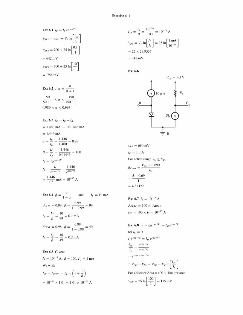
Exercise 6–1 Ex: 6.1 I V IS 10 C S ISB 10 A β 100 V C BE T ...qli/ECE333/Chapter 06 ISM.pdf= 10...
38
Exercise 6–1 Ex: 6.1 i C = I S e v BE /V T v BE2 − v BE1 = V T ln i C2 i C1 v BE2 = 700 + 25 ln 0.1 1 = 642 mV v BE3 = 700 + 25 ln 10 1 = 758 mV Ex: 6.2 ∴ α = β β + 1 50 50 + 1 <α< 150 150 + 1 0.980 <α< 0.993 Ex: 6.3 I C = I E − I B = 1.460 mA − 0.01446 mA = 1.446 mA α = I C I E = 1.446 1.460 = 0.99 β = I C I B = 1.446 0.01446 = 100 I C = I S e v BE /V T I S = I C e v BE /V T = 1.446 e 700/25 = 1.446 e 28 mA = 10 −15 A Ex: 6.4 β = α 1 − α and I C = 10 mA For α = 0.99, β = 0.99 1 − 0.99 = 99 I B = I C β = 10 99 = 0.1 mA For α = 0.98, β = 0.98 1 − 0.98 = 49 I B = I C β = 10 49 = 0.2 mA Ex: 6.5 Given: I S = 10 −16 A, β = 100, I C = 1 mA We write I SE = I SC /α = I S = 1 + 1 β = 10 −16 × 1.01 = 1.01 × 10 −16 A I SB = I S β = 10 −16 100 = 10 −18 A V BE = V T ln I C I S = 25 ln 1 mA 10 −16 = 25 × 29.9336 = 748 mV Ex: 6.6 V CC 5 V R C B 10 A bI B E C v BE = 690 mV I C = 1 mA For active range V C ≥ V B , R Cmax = V CC − 0.690 I C = 5 − 0.69 1 = 4.31 k Ex: 6.7 I S = 10 −15 A Area C = 100 × Area E I SC = 100 × I S = 10 −13 A Ex: 6.8 i C = I S e v BE /V T − I SC e v BC /V T for i C = 0 I S e v BE /V T = I SC e v BC /V T I SC I S = e v BE /V T e v BC /V T = e (v BE −v BC )/V T ∴ V CE = V BE − V BC = V T ln I SC I S For collector Area = 100 × Emitter area V CE = 25 ln 100 1 = 115 mV
Transcript of Exercise 6–1 Ex: 6.1 I V IS 10 C S ISB 10 A β 100 V C BE T ...qli/ECE333/Chapter 06 ISM.pdf= 10...
SEDRA-ISM: “E-CH06” — 2014/11/3 — 11:55 — PAGE 1 — #1
Exercise 6–1
Ex: 6.1 iC = IS evBE/VT
vBE2 − vBE1 = VT ln
[iC2
iC1
]
vBE2 = 700 + 25 ln
[0.1
1
]
= 642 mV
vBE3 = 700 + 25 ln
[10
1
]
= 758 mV
Ex: 6.2 ∴ α = β
β + 1
50
50 + 1< α <
150
150 + 1
0.980 < α < 0.993
Ex: 6.3 IC = IE − IB
= 1.460 mA − 0.01446 mA
= 1.446 mA
α = IC
IE= 1.446
1.460= 0.99
β = IC
IB= 1.446
0.01446= 100
IC = ISevBE/VT
IS = IC
evBE/VT= 1.446
e700/25
= 1.446
e28mA = 10−15 A
Ex: 6.4 β = α
1 − αand IC = 10 mA
For α = 0.99, β = 0.99
1 − 0.99= 99
IB = IC
β= 10
99= 0.1 mA
For α = 0.98, β = 0.98
1 − 0.98= 49
IB = IC
β= 10
49= 0.2 mA
Ex: 6.5 Given:
IS = 10−16 A, β = 100, IC = 1 mA
We write
ISE = ISC/α = IS =(
1 + 1
β
)
= 10−16 × 1.01 = 1.01 × 10⁻¹⁶ A
ISB = IS
β= 10−16
100= 10−18 A
VBE = VT ln
[IC
IS
]= 25 ln
[1 mA
10−16
]
= 25 × 29.9336
= 748 mV
Ex: 6.6
VCC � �5 V
RC
B
10 �A
bIB
E
C
vBE = 690 mV
IC = 1 mA
For active range VC ≥ VB,
RCmax = VCC − 0.690
IC
= 5 − 0.69
1
= 4.31 k�
Ex: 6.7 IS = 10−15 A
AreaC = 100 × AreaE
ISC = 100 × IS = 10−13 A
Ex: 6.8 iC = ISevBE/VT − ISCevBC /VT
for iC = 0
ISevBE/VT = ISCevBC /VT
ISC
IS= evBE/VT
evBC /VT
= e(vBE−vBC )/VT
∴ VCE = VBE − VBC = VT ln
[ISC
IS
]
For collector Area = 100 × Emitter area
VCE = 25 ln
[100
1
]= 115 mV
SEDRA-ISM: “E-CH06” — 2014/11/3 — 11:55 — PAGE 2 — #2
Exercise 6–2
Ex: 6.9 IC = ISevBE/VT − ISCevBC /VT
IB = IS
βevBE/VT + ISCevBC /VT
β forced = IC
IB
∣∣∣∣sat
< β
= βISevBE/VT − ISCevBC /VT
ISevBE/VT + βI SCevBC /VT
= βISe(vBE−vBC )/VT − ISC
ISe(vBE−vBC )/VT + βISC
= βeVCE sat/VT − ISC/IS
eVCE sat/VT + βISC/ISQ.E.D.
β forced = 100e200/25 − 100
e200/25 + 100 × 100
= 100 × 0.2219 ≈ 22.2
Ex: 6.10
IS /a
ISevEB/VT
� aiE
2 mA
E
B
C
�10 V
IE = IS
αevBE/VT
2 mA = 51
5010−14evBE/VT
VBE = 25 ln
[2
103 × 50
51× 1014
]
= 650 mV
IC = β
β + 1IE = 50
51× 2
= 1.96 mA
IB = IC
β= 1.96
50⇒ 39.2 μA
Ex: 6.11 IC = ISevBE/VT = 1.5 A
∴ VBE = VT ln[1.5/10−11
]= 25 × 25.734
= 643 mV
Ex: 6.12
�1.5 V
�1.5 V
2 mA
2 mA
�
a
�VBE
VC � 0.5 V
VE � �VBE
IE � ( )
RC
RE
RC = 1.5 − VC
IC= 1.5 − 0.5
2
= 0.5 k� = 500 �
Since at IC = 1 mA, VBE = 0.8 V, then atIC = 2 mA,
VBE = 0.8 + 0.025 ln
(2
1
)
= 0.8 + 0.017
= 0.817 V
VE = −VBE = −0.817 V
IE = 2 mA
α= 2
0.99= 2.02 mA
IE = VE − (−1.5)
RE
Thus,
RE = −0.817 + 1.5
2.02= 0.338 k�
= 338 �
Ex: 6.13
�10 V
�10 V
IC
IE
IB
VC
VE � �0.7 V
10 k�
5 k�
SEDRA-ISM: “E-CH06” — 2014/11/3 — 11:55 — PAGE 3 — #3
Exercise 6–3
IE = VE − (−10)
10= −0.7 + 10
10
= 0.93 mA
Assuming active-mode operation,
IB = IE
β + 1= 0.93
50 + 1= 0.0182 mA
= 18.2 μA
IC = IE − IB = 0.93 − 0.0182 = 0.91 mA
VC = 10 − IC × 5
= 10 − 0.91 × 5 = 5.45 V
Since VC > VB, the transistor is operating in theactive mode, as assumed.
Ex: 6.14
�10 V
�10 V
IE
IC
IB
IB
VE
VB
VC
5 k�
100 k�
5 k�
VB = 1.0 V
Thus,
IB = VB
100 k�= 0.01 mA
VE = +1.7 V
Thus,
IE = 10 − VE
5 k�= 10 − 1.7
5= 1.66 mA
and
β + 1 = IE
IB= 1.66
0.01= 166
⇒ β = 165
α = β
β + 1= 165
165 + 1= 0.994
Assuming active-mode operation,
IC = αIE = 0.994 × 1.66 = 1.65 mA
and
VC = −10 + 1.65 × 5 = −1.75 V
Since VC < VB, the transistor is indeed operatingin the active mode.
Ex: 6.15
�5 V
IC
VE
VC
RC � 1 k�
2 mA
The transistor is operating at a constant emittercurrent. Thus, a change in temperature of +30◦Cresults in a change in VEB by
�VEB = −2 mV × 30 = −60 mV
Thus,
�VE = −60 mV
Since the collector current remains unchanged atαIE , the collector voltage does not change:
�VC = 0 V
Ex: 6.16 Refer to Fig. 6.19(a):
iC = ISevBE/VT + vCE
ro(1)
Now using Eqs. (6.21) and (6.22), we can expressro as
ro = VA
ISevBE/VT
Substituting in Eq. (1), we have
iC = ISevBE/VT
(1 + vCE
VA
)
which is Eq. (6.18). Q.E.D.
Ex: 6.17 ro = VA
IC= 100
IC
At IC = 0.1 mA, ro = 1 M�
At IC = 1 mA, ro = 100 k�
At IC = 10 mA, ro = 10 k�
SEDRA-ISM: “E-CH06” — 2014/11/3 — 11:55 — PAGE 4 — #4
Exercise 6–4
Ex: 6.18 �IC = �VCE
ro
where
ro = VA
IC= 100
1= 100 k�
�IC = 11 − 1
100= 0.1 mA
Thus, IC becomes 1.1 mA.
Ex: 6.19
VCC � 10 V
�
�
��
IB
IC
VBB
RC � 10 k�
VBE � 0.7 V
VCE
RB � 10 k�
(a) For operation in the active mode withVCE = 5 V,
IC = VCC − VC
RC= 10 − 5
10= 0.5 mA
IB = IC
β= 0.5
50= 0.01 mA
VBB = VBE + IBRB
= 0.7 + 0.01 × 10 = 0.8 V
(b) For operation at the edge of saturation,
VCE = 0.3 V
IC = VCC − VCE
RC= 10 − 0.3
10= 0.97 mA
IB = IC
β= 0.97
50= 0.0194 mA
VBB = VB + IBRB
= 0.7 + 0.0194 × 10 = 0.894 V
(c) For operation deep in saturation withβforced = 10, we have
VCE � 0.2 V
IC = 10 − 0.2
10= 0.98 mA
IB = IC
βforced= 0.98
10= 0.098 mA
VBB = VB + IBRB
= 0.7 + 0.098 × 10 = 1.68 V
Ex: 6.20 For VBB = 0 V, IB = 0 and the transistoris cut off. Thus,
IC = 0
and
VC = VCC = +10 V
Ex: 6.21 Refer to the circuit in Fig. 6.22 and letVBB = 1.7 V. The current IB can be found from
IB = VBB − VB
RB= 1.7 − 0.7
10= 0.1 mA
Assuming operation in the active mode,
IC = β IB = 50 × 0.1 = 5 mA
Thus,
VC = VCC − RCIC
= 10 − 1 × 5 = 5 V
which is greater than VB, verifying that thetransistor is operating in the active mode, asassumed.
(a) To obtain operation at the edge of saturation,RC must be increased to the value that results inVCE = 0.3 V:
RC = VCC − 0.3
IC
= 10 − 0.3
5= 1.94 k�
(b) Further increasing RC results in the transistoroperating in saturation. To obtain saturation-modeoperation with VCE = 0.2 V and βforced = 10,we use
IC = βforced × IB
= 10 × 0.1 = 1 mA
The value of RC required can be found from
RC = VCC − VCE
IC
= 10 − 0.2
1= 9.8 k�
Ex: 6.22 Refer to the circuit in Fig. 6.23(a) withthe base voltage raised from 4 V to VB. If at thisvalue of VB, the transistor is at the edge ofsaturation then,
VC = VB − 0.4 V
Since IC � IE , we can write
10 − VC
RC= VE
RE= VB − 0.7
RE
SEDRA-ISM: “E-CH06” — 2014/11/3 — 11:55 — PAGE 5 — #5
Exercise 6–5
Thus,
10 − (VB − 0.4)
4.7= VB − 0.7
3.3
⇒ VB = +4.7 V
Ex: 6.23
�10 V
0.5 mA
0.5 mA
VC � �6 V
RC
VE � �3.3 V
RE
VB � �4 V
To establish a reverse-bias voltage of 2 V acrossthe CBJ,
VC = +6 V
From the figure we see that
RC = 10 − 6
0.5= 8 k�
and
RE = 3.3
0.5= 6.6 k�
where we have assumed α � 1.
Ex: 6.24
�10 V
VB � 0.5
IC � 5IB
4.7 k�
VB � 0.7
3.3 k�
VB
IB
6IB
The figure shows the circuit with the base voltageat VB and the BJT operating in saturation withVCE = 0.2 V and βforced = 5.
IC = 5IB = 10 − (VB − 0.5)
4.7(1)
IE = 6IB = VB − 0.7
3.3(2)
Dividing Eq. (1) by Eq. (2), we have
5
6= 10.5 − VB
VB − 0.7× 3.3
4.7
⇒ VB = +5.18 V
Ex: 6.25 Refer to the circuit in Fig. 6.26(a). Thelargest value for RC while the BJT remains in theactive mode corresponds to
VC = +0.4 V
Since the emitter and collector currents remainunchanged, then from Fig. 6.26(b) we obtain
IC = 4.6 mA
Thus,
RC = VC − (−10)
IC
= +0.4 + 10
4.6= 2.26 k�
Ex: 6.26
�10 V
�10 V
VE � �0.7 VRE
VC � �4 V
RC
1 mA
1 mA
For a 4-V reverse-biased voltage across the CBJ,
VC = −4 V
Refer to the figure.
IC = 1 mA = VC − (−10)
RC
⇒ RC = −4 + 10
1= 6 k�
RE = 10 − VE
IE
Assuming α = 1,
RE = 10 − 0.7
1= 9.3 k�

SEDRA-ISM: “E-CH06” — 2014/11/3 — 11:55 — PAGE 6 — #6
Exercise 6–6
Ex: 6.27 Refer to the circuit in Fig. 6.27:
IB = 5 − 0.7
100= 0.043 mA
To ensure that the transistor remains in the activemode for β in the range 50 to 150, we need toselect RC so that for the highest collector currentpossible, the BJT reaches the edge of saturation,that is, VCE = 0.3 V. Thus,
VCE = 0.3 = 10 − RCICmax
where
ICmax = βmaxIB
= 150 × 0.043 = 6.45 mA
Thus,
RC = 10 − 0.3
6.45= 1.5 k�
For the lowest β,
IC = βminIB
= 50 × 0.043 = 2.15 mA
and the corresponding VCE is
VCE = 10 − RCIC = 10 − 1.5 × 2.15
= 6.775 V
Thus, VCE will range from 0.3 V to 6.8 V.
Ex: 6.28 Refer to the solution of Example 6.10.
IE = VBB − VBE
RE + [RBB/(β + 1)]
= 5 − 0.7
3 + (33.3/51)= 1.177 mA
IC = αIE = 0.98 × 1.177 = 1.15 mA
Thus the current is reduced by
�IC = 1.28 − 1.15 = 0.13 mA
which is a −10% change.
Ex: 6.29 Refer to the circuit in Fig. 6.30(b). Thetotal current drawn from the power supply is
I = 0.103 + 1.252 + 2.78 = 4.135 mA
Thus, the power dissipated in the circuit is
P = 15 V × 4.135 mA = 62 mW
Ex: 6.30
�15 V
2.78 mA
VE3
VC2
IC3/b
IC3
�9.44 V
2.75 mA
2.7 k�470 �
2 k�
Q2
Q3
IC3a
From the figure we see that
VE3 = IC3
α× 0.47
VC2 = VE3 + 0.7 = IC3
α× 0.47 + 0.7 (1)
A node equation at the collector of Q2 yields
2.75 = VC2
2.7+ IC3
β
Substituting for VC2 from Eq. (1), we obtain
2.75 = (0.47 IC3/α) + 0.7
2.7+ IC3
β
Substituting α = 0.99 and β = 100 and solvingfor IC3 results in
IC3 = 13.4 mA
Now, VE3 and VC2 can be determined:
VE3 = IC3
α× 0.47 = 13.4
0.99× 0.47 = +6.36 V
VC2 = VE3 + 0.7 = +7.06 V
Ex: 6.31
�5 V
�5 V
�5 V VE � �IE � 1
IB
IE
0
IE
10 k�
1 k�
Q1 off
Q2 on
SEDRA-ISM: “E-CH06” — 2014/11/3 — 11:55 — PAGE 7 — #7
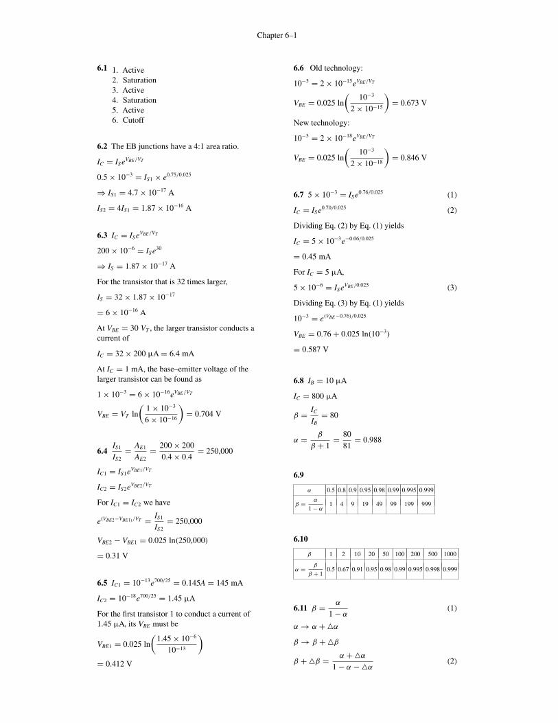
Exercise 6–7
From the figure we see that Q1 will be off and Q2
will be on. Since the base of Q2 will be at avoltage higher than −5 V, transistor Q2 will beoperating in the active mode. We can write a loopequation for the loop containing the 10-k�
resistor, the EBJ of Q2 and the 1-k� resistor:
−IE × 1 − 0.7 − IB × 10 = −5
Substituting IB = IE/(β + 1) = IE/101 andrearranging gives
IE = 5 − 0.710
101+ 1
= 3.9 mA
Thus,
VE = −3.9 V
VB2 = −4.6 V
IB = 0.039 mA
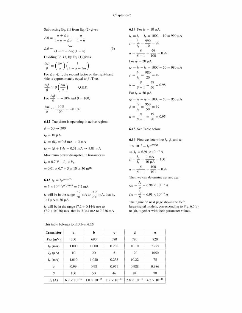
Ex: 6.32 With the input at + 10 V, there is astrong possibility that the conducting transistor
This figure belongs to Exercise 6.32.
�5 V
�5.5 V
�5 V
�10 V
10 � 5.5 � 0.45 mA10
�4.8 V
�
�10 k�
1 k�
Q1 on VCEsat � 0.2 V
Q2 off
4 1
2
4.8mA
35
Q1 will be saturated. Assuming this to be the case,the analysis steps will be as follows:
VCEsat|Q1= 0.2 V
VE = 5 V − VCEsat = +4.8 V
IE1 = 4.8 V
1 k�= 4.8 mA
VB1 = VE + VBE1 = 4.8 + 0.7 = +5.5 V
IB1 = 10 − 5.5
10= 0.45 mA
IC1 = IE1 − IB1 = 4.8 − 0.45 = 4.35 mA
βforced = IC
IB= 4.35
0.45= 9.7
which is lower than βmin, verifying that Q1 isindeed saturated.
Finally, since Q2 is off,
IC2 = 0
Ex: 6.33 VO = +10 − BVBCO = 10 − 70
= −60 V
Chapter 6–1
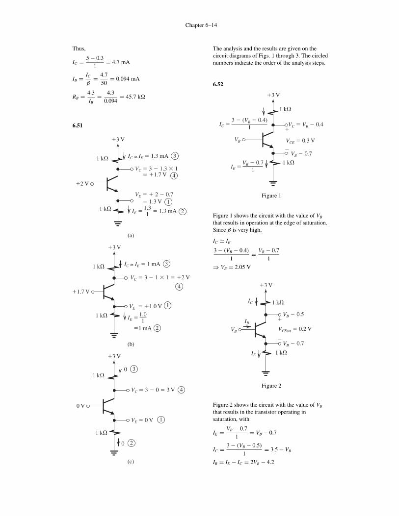
6.1 1. Active2. Saturation3. Active4. Saturation5. Active6. Cutoff
6.2 The EB junctions have a 4:1 area ratio.
IC = ISeVBE/VT
0.5 × 10−3 = IS1 × e0.75/0.025
⇒ IS1 = 4.7 × 10⁻¹⁷ A
IS2 = 4IS1 = 1.87 × 10⁻¹⁶ A
6.3 IC = ISeVBE/VT
200 × 10−6 = ISe30
⇒ IS = 1.87 × 10⁻¹⁷ A
For the transistor that is 32 times larger,
IS = 32 × 1.87 × 10−17
= 6 × 10⁻¹⁶ A
At VBE = 30 VT , the larger transistor conducts acurrent of
IC = 32 × 200 μA = 6.4 mA
At IC = 1 mA, the base–emitter voltage of thelarger transistor can be found as
1 × 10−3 = 6 × 10⁻¹⁶eVBE/VT
VBE = VT ln
(1 × 10⁻³
6 × 10⁻¹⁶
)= 0.704 V
6.4IS1
IS2= AE1
AE2= 200 × 200
0.4 × 0.4= 250,000
IC1 = IS1eVBE1/VT
IC2 = IS2eVBE2/VT
For IC1 = IC2 we have
e(VBE2−VBE1)/VT = IS1
IS2= 250,000
VBE2 − VBE1 = 0.025 ln(250,000)
= 0.31 V
6.5 IC1 = 10−13e700/25 = 0.145A = 145 mA
IC2 = 10−18e700/25 = 1.45 μA
For the first transistor 1 to conduct a current of1.45 μA, its VBE must be
VBE1 = 0.025 ln
(1.45 × 10⁻⁶
10−13
)
= 0.412 V
6.6 Old technology:
10−3 = 2 × 10⁻¹⁵eVBE/VT
VBE = 0.025 ln
(10−3
2 × 10⁻¹⁵
)= 0.673 V
New technology:
10−3 = 2 × 10⁻¹⁸eVBE/VT
VBE = 0.025 ln
(10−3
2 × 10⁻¹⁸
)= 0.846 V
6.7 5 × 10−3 = ISe0.76/0.025 (1)
IC = ISe0.70/0.025 (2)
Dividing Eq. (2) by Eq. (1) yields
IC = 5 × 10⁻³e−0.06/0.025
= 0.45 mA
For IC = 5 μA,
5 × 10−6 = ISeVBE/0.025 (3)
Dividing Eq. (3) by Eq. (1) yields
10−3 = e(VBE−0.76)/0.025
VBE = 0.76 + 0.025 ln(10−3)
= 0.587 V
6.8 IB = 10 μA
IC = 800 μA
β = IC
IB= 80
α = β
β + 1= 80
81= 0.988
6.9
α 0.5 0.8 0.9 0.95 0.98 0.99 0.995 0.999
β = α
1 − α1 4 9 19 49 99 199 999
6.10
β 1 2 10 20 50 100 200 500 1000
α = β
β + 10.5 0.67 0.91 0.95 0.98 0.99 0.995 0.998 0.999
6.11 β = α
1 − α(1)
α → α + �α
β → β + �β
β + �β = α + �α
1 − α − �α(2)
Chapter 6–2
Subtracting Eq. (1) from Eq. (2) gives
�β = α + �α
1 − α − �α− α
1 − α
�β = �α
(1 − α − �α)(1 − α)(3)
Dividing Eq. (3) by Eq. (1) gives
�β
β=
(�α
α
) (1
1 − α − �α
)
For �α � 1, the second factor on the right-handside is approximately equal to β. Thus
�β
β� β
(�α
α
)Q.E.D.
For�β
β= −10% and β = 100,
�α
α� −10%
100= −0.1%
6.12 Transistor is operating in active region:
β = 50 → 300
IB = 10 μA
IC = βIB = 0.5 mA → 3 mA
IE = (β + 1)IB = 0.51 mA → 3.01 mA
Maximum power dissipated in transistor is
IB × 0.7 V + IC × VC
= 0.01 × 0.7 + 3 × 10 � 30 mW
6.13 iC = ISevBE/VT
= 5 × 10⁻¹⁵e0.7/0.025 = 7.2 mA
iB will be in the range7.2
50mA to
7.2
200mA, that is,
144 μA to 36 μA.
iE will be in the range (7.2 + 0.144) mA to(7.2 + 0.036) mA, that is, 7.344 mA to 7.236 mA.
This table belongs to Problem 6.15.
Transistor a b c d e
VBE (mV) 700 690 580 780 820
IC (mA) 1.000 1.000 0.230 10.10 73.95
IB (μA) 10 20 5 120 1050
IE (mA) 1.010 1.020 0.235 10.22 75
α 0.99 0.98 0.979 0.988 0.986
β 100 50 46 84 70
IS (A) 6.9 × 10⁻¹⁶ 1.0 × 10⁻¹⁵ 1.9 × 10⁻¹⁴ 2.8 × 10⁻¹⁶ 4.2 × 10⁻¹⁶
6.14 For iB = 10 μA,
iC = iE − iB = 1000 − 10 = 990 μA
β = iC
iB= 990
10= 99
α = β
β + 1= 99
100= 0.99
For iB = 20 μA,
iC = iE − iB = 1000 − 20 = 980 μA
β = iC
iB= 980
20= 49
α = β
β + 1= 49
50= 0.98
For iB = 50 μA,
iC = iE − iB = 1000 − 50 = 950 μA
β = iC
iB= 950
50= 19
α = β
β + 1= 19
20= 0.95
6.15 See Table below.
6.16 First we determine IS , β, and α:
1 × 10−3 = ISe700/25
⇒ IS = 6.91 × 10⁻¹⁶ A
β = IC
IB= 1 mA
10 μA= 100
α = β
β + 1= 100
101= 0.99
Then we can determine ISE and ISB:
ISE = IS
α= 6.98 × 10⁻¹⁶ A
ISB = IS
β= 6.91 × 10⁻¹⁸ A
The figure on next page shows the fourlarge-signal models, corresponding to Fig. 6.5(a)to (d), together with their parameter values.

Chapter 6–3
DE
iB
a � 0.99ISE � 6.98 � 10�16 A
aiE
vBE
C
E
B
iC
iE
�
ISE � IS/a�
(b)
B CiC
biBvBE
ISB �
iB
DB
E
�
�
IS
iE
b
b � 100ISB � 6.91 � 10�18 A
(d)
6.17
VC
VE
DE
B
C
�5 V
2 mA
E
2 k�
aiE
iE
The figure shows the circuit, where
α = β
β + 1= 100
101= 0.99
ISE = IS
α= 5 × 10⁻¹⁵
0.99= 5.05 × 100−15 A
The voltage at the emitter VE is
VE = −VDE
= −VT ln(IE/ISE)
= −0.025 ln
(2 × 10⁻³
5.05 × 10⁻¹⁵
)
= −0.668 V
The voltage at the collector VC is found from
VC = 5 − IC × 2
= 5 − αIE × 2
= 5 − 0.99 × 2 × 2 = 1.04 V
6.18 Refer to the circuit in Fig. 6.6(b).
ISB = IS
β= 5 × 10⁻¹⁵
50= 10−16 A
IB = IC
β= 0.5 × 10⁻³
50= 10−5 A
VB = VBE = VT ln
(IB
ISB
)
= 0.025 ln
(10−5
10−16
)
= 0.633 V
We can determine RB from
RB = VCC − VB
IB
= 15 − 0.633
10−5= 1.44 M�
Chapter 6–4
To obtain VCE = 1 V, we select RC according to
RC = VCC − VCE
IC
= 15 − 1
0.5= 28 k�
6.19 IS = 10−15 A
Thus, a forward-biased EBJ conducting a currentof 1 mA will have a forward voltage drop VBE :
VBE = VT ln
(I
IS
)
= 0.025 ln
(10−3
10−15
)= 0.691 V
ISC = 100IS = 10−13 A
Thus, a forward-biased CBJ conducting a 1-mAcurrent will have a forward voltage drop VBC :
VBC = VT ln
(1 × 10⁻³
1 × 10⁻¹³
)= 0.576 V
When forward-biased with 0.5 V, the emitter–basejunction conducts
I = ISe0.5/0.025
= 10−15e0.5/0.025 = 0.49 μA
and the CBJ conducts
I = ISCe0.5/0.025
= 10−13e0.5/0.025 = 48.5 μA
6.20 The equations utilized are
vBC = vBE − vCE = 0.7 − vCE
iBC = ISCevBC /VT = 10−13evBC /0.025
iBE = ISBevBE/VT = 10−17e0.7/0.025
iB = iBC + iBE
iC = ISevBE/VT − iBC = 10−15e0.7/0.025 − iBC
Performing these calculations for vCE = 0.4 V,0.3 V, and 0.2 V, we obtain the results shown inthe table below.
This table belongs to Problem 6.20.
v CE (V) v BC (V) iBC (μA) iBE (μA) iB (μA) iC (mA) iC/iB
0.4 0.3 0.016 14.46 14.48 1.446 100
0.3 0.4 0.89 14.46 15.35 1.445 94
0.2 0.5 48.5 14.46 62.96 1.398 29
6.21 Dividing Eq. (6.14) by Eq. (6.15) andsubstituting iC/iB = βforced gives
βforced = ISevBE/VT − ISCevBC /VT
(IS/β)evBE/VT + ISCevBC /VT
Dividing the numerator and denominator of theright-hand side by ISCevBC /VT and replacingvBE − vBC by VCEsat gives
βforced =
(IS
ISC
)eVCEsat/VT − 1
1
β
(IS
ISC
)eVCEsat/VT + 1
This equation can be used to obtain eVCEsat/VT andhence VCEsat as(
IS
ISC
)eVCEsat/VT = 1 + βforced
1 − βforced/β
⇒ VCEsat = VT ln
[ISC
IS
1 + βforced
1 − βforced/β
]Q.E.D.
For β = 100 and ISC/IS = 100, we can use thisequation to obtain VCEsat corresponding to thegiven values of βforced. The results are as follows:
βforced 50 10 5 1
VCEsat (V) 0.231 0.178 0.161 0.133
6.22
The emitter–base voltage VEB is found as thevoltage drop across the diode DB, whose scale
Chapter 6–5
current is ISB = IS/β, it is conducting a 10-μAcurrent. Thus,
VEB = VT ln
(10 μA
ISB
)
where
ISB = IS
β= 10−14
50= 2 × 10⁻¹⁶ A
VEB = 0.025 ln
(10 × 10−6
2 × 10⁻¹⁶
)
= 0.616 V
Thus,
VB = −VEB = −0.616 V
The collector current can be found as
IC = βIB
= 50 × 10 = 500 μA = 0.5 mA
The collector voltage can now be obtained from
VC = −5 + IC × 8.2 = −5 + 0.5 × 8.2 = −0.9 V
The emitter current can be found as
IE = IB + IC = 10 + 500 = 510 μA
= 0.51 mA
6.23 At iC = 1 mA, vEB = 0.7 V
At iC = 10 mA,
vEB = 0.7 + VT ln
(10
1
)
= 0.7 + 0.025 ln(10) = 0.758 V
At iC = 100 mA,
vEB = 0.7 + 0.025 ln
(100
1
)
= 0.815 V
Note that vEB increases by about 60 mV for everydecade increase in iC .
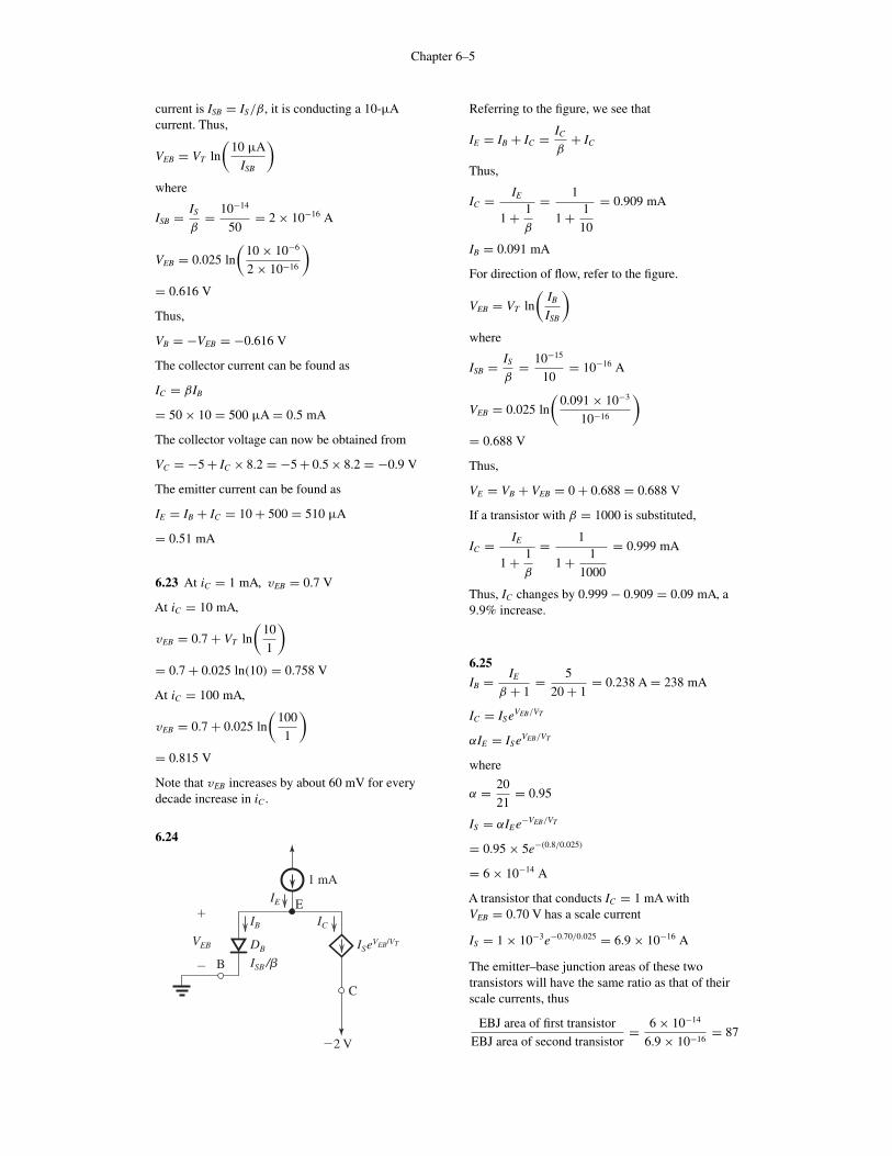
6.24
Referring to the figure, we see that
IE = IB + IC = IC
β+ IC
Thus,
IC = IE
1 + 1
β
= 1
1 + 1
10
= 0.909 mA
IB = 0.091 mA
For direction of flow, refer to the figure.
VEB = VT ln
(IB
ISB
)
where
ISB = IS
β= 10−15
10= 10−16 A
VEB = 0.025 ln
(0.091 × 10⁻³
10−16
)
= 0.688 V
Thus,
VE = VB + VEB = 0 + 0.688 = 0.688 V
If a transistor with β = 1000 is substituted,
IC = IE
1 + 1
β
= 1
1 + 1
1000
= 0.999 mA
Thus, IC changes by 0.999 − 0.909 = 0.09 mA, a9.9% increase.
6.25
IB = IE
β + 1= 5
20 + 1= 0.238 A = 238 mA
IC = ISeVEB/VT
αIE = ISeVEB/VT
where
α = 20
21= 0.95
IS = αIEe−VEB/VT
= 0.95 × 5e−(0.8/0.025)
= 6 × 10⁻¹⁴ A
A transistor that conducts IC = 1 mA withVEB = 0.70 V has a scale current
IS = 1 × 10⁻³e−0.70/0.025 = 6.9 × 10⁻¹⁶ A
The emitter–base junction areas of these twotransistors will have the same ratio as that of theirscale currents, thus
EBJ area of first transistor
EBJ area of second transistor= 6 × 10⁻¹⁴
6.9 × 10−16= 87
Chapter 6–6
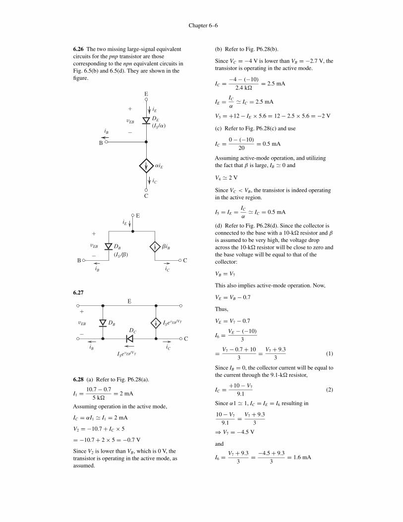
6.26 The two missing large-signal equivalentcircuits for the pnp transistor are thosecorresponding to the npn equivalent circuits inFig. 6.5(b) and 6.5(d). They are shown in thefigure.
DE
(IS/a)
iE
iB
aiE
E
C
B
iC
vEB
�
�
6.27
6.28 (a) Refer to Fig. P6.28(a).
I1 = 10.7 − 0.7
5 k�= 2 mA
Assuming operation in the active mode,
IC = αI1 � I1 = 2 mA
V2 = −10.7 + IC × 5
= −10.7 + 2 × 5 = −0.7 V
Since V2 is lower than VB, which is 0 V, thetransistor is operating in the active mode, asassumed.
(b) Refer to Fig. P6.28(b).
Since VC = −4 V is lower than VB = −2.7 V, thetransistor is operating in the active mode.
IC = −4 − (−10)
2.4 k�= 2.5 mA
IE = IC
α� IC = 2.5 mA
V3 = +12 − IE × 5.6 = 12 − 2.5 × 5.6 = −2 V
(c) Refer to Fig. P6.28(c) and use
IC = 0 − (−10)
20= 0.5 mA
Assuming active-mode operation, and utilizingthe fact that β is large, IB � 0 and
V4 � 2 V
Since VC < VB, the transistor is indeed operatingin the active region.
I5 = IE = IC
α� IC = 0.5 mA
(d) Refer to Fig. P6.28(d). Since the collector isconnected to the base with a 10-k� resistor and β
is assumed to be very high, the voltage dropacross the 10-k� resistor will be close to zero andthe base voltage will be equal to that of thecollector:
VB = V7
This also implies active-mode operation. Now,
VE = VB − 0.7
Thus,
VE = V7 − 0.7
I6 = VE − (−10)
3
= V7 − 0.7 + 10
3= V7 + 9.3
3(1)
Since IB = 0, the collector current will be equal tothe current through the 9.1-k� resistor,
IC = +10 − V7
9.1(2)
Since α1 � 1, IC = IE = I6 resulting in
10 − V7
9.1= V7 + 9.3
3
⇒ V7 = −4.5 V
and
I6 = V7 + 9.3
3= −4.5 + 9.3
3= 1.6 mA
Chapter 6–7
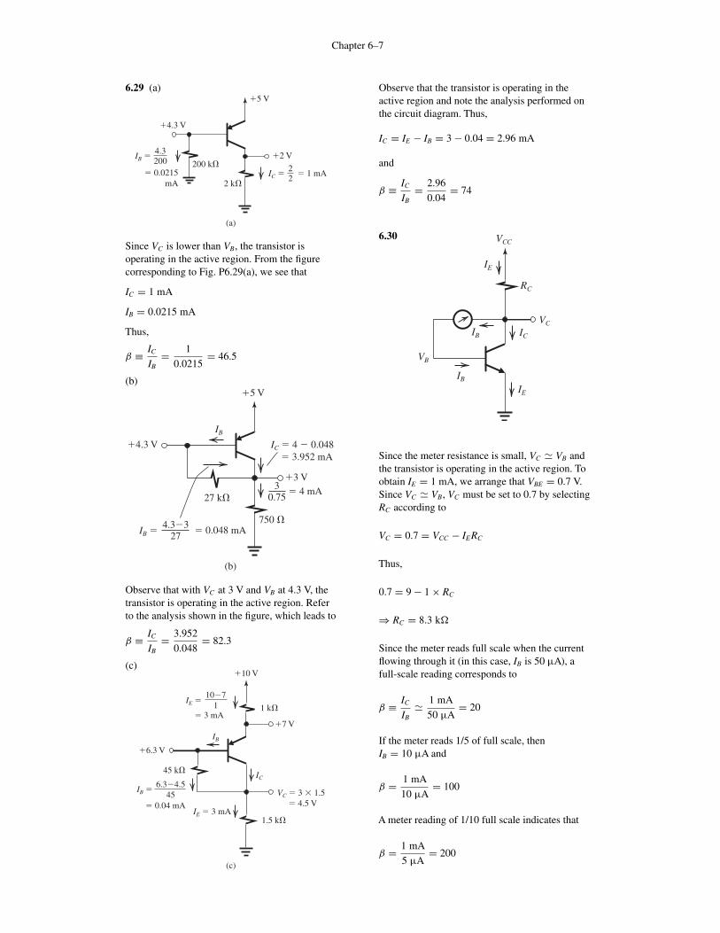
6.29 (a)
Since VC is lower than VB, the transistor isoperating in the active region. From the figurecorresponding to Fig. P6.29(a), we see that
IC = 1 mA
IB = 0.0215 mA
Thus,
β ≡ IC
IB= 1
0.0215= 46.5
(b)
Observe that with VC at 3 V and VB at 4.3 V, thetransistor is operating in the active region. Referto the analysis shown in the figure, which leads to
β ≡ IC
IB= 3.952
0.048= 82.3
(c)
Observe that the transistor is operating in theactive region and note the analysis performed onthe circuit diagram. Thus,
IC = IE − IB = 3 − 0.04 = 2.96 mA
and
β ≡ IC
IB= 2.96
0.04= 74
6.30
IE
RC
VC
VCC
IC
IE
VB
IB
IB
Since the meter resistance is small, VC � VB andthe transistor is operating in the active region. Toobtain IE = 1 mA, we arrange that VBE = 0.7 V.Since VC � VB, VC must be set to 0.7 by selectingRC according to
VC = 0.7 = VCC − IERC
Thus,
0.7 = 9 − 1 × RC
⇒ RC = 8.3 k�
Since the meter reads full scale when the currentflowing through it (in this case, IB is 50 μA), afull-scale reading corresponds to
β ≡ IC
IB� 1 mA
50 μA= 20
If the meter reads 1/5 of full scale, thenIB = 10 μA and
β = 1 mA
10 μA= 100
A meter reading of 1/10 full scale indicates that
β = 1 mA
5 μA= 200
Chapter 6–8
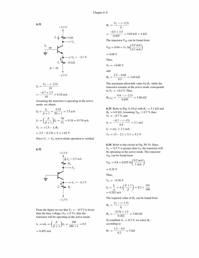
6.31�2.5 V
�2.5 V
VC
5 k�
b � 50
VE � �0.7 V
10 k�IE
IC
IB
IE = VE − (−2.5)
10
= −0.7 + 2.5
10= 0.18 mA
Assuming the transistor is operating in the activemode, we obtain
IB = IE
β + 1= 0.18
50 + 1= 3.5 μA
IC =(
β
β + 1
)IE = 50
51× 0.18 = 0.176 mA
VC = +2.5 − ICRC
= 2.5 − 0.176 × 5 = 1.62 V
Since VC > VB, active-mode operation is verified.
6.32�2.5 V
�2.5 V
VE
RE
VC ��0.5 V
IE � 0.5 mA
RCIC
From the figure we see that VC = −0.5 V is lowerthan the base voltage (VB = 0 V); thus thetransistor will be operating in the active mode.
IC = αIE =(
β
β + 1
)IE = 100
100 + 1× 0.5
= 0.495 mA
RC = VC − (−2.5)
IC
= −0.5 + 2.5
0.495= 4.04 k� � 4 k�
The transistor VEB can be found from
VEB = 0.64 + VT ln
(0.5 mA
0.1 mA
)
= 0.68 V
Thus,
VE = +0.68 V
and
RE = 2.5 − 0.68
0.5= 3.64 k�
The maximum allowable value for RC while thetransistor remains in the active mode correspondsto VC = +0.4 V. Thus,
RCmax = 0.4 − (−2.5)
0.495= 5.86 k�
6.33 Refer to Fig. 6.15(a) with RC = 5.1 k� andRE = 6.8 k�. Assuming VBE � 0.7 V, thenVE = −0.7 V, and
IE = −0.7 − (−15)
6.8= 2.1 mA
IC = αIE � 2.1 mA
VC = 15 − 2.1 × 5.1 � 4.3 V
6.34 Refer to the circuit in Fig. P6.34. SinceVC = 0.5 V is greater than VB, the transistor willbe operating in the active mode. The transistorVBE can be found from
VBE = 0.8 + 0.025 ln
(0.2 mA
1 mA
)
= 0.76 V
Thus,
VE = −0.76 V
IE = IC
α= IC
(β + 1
β
)= 0.2 × 101
100= 0.202 mA
The required value of RE can be found from
RE = VE − (−1.5)
IE
RE = −0.76 + 1.5
0.202= 3.66 k�
To establish VC = 0.5 V, we select RC
according to
RC = 1.5 − 0.5
0.2= 5 k�
Chapter 6–9
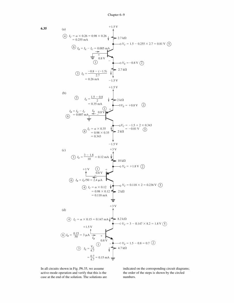
6.35 �1.5 V
�
�
�1.5 V
VC � 1.5 � 0.255 � 2.7 � 0.81 V
2.7 k�
0.8 V
2.7 k�
IC � a � 0.26 � 0.98 � 0.26 � 0.255 mA
� 0.26 mA
IB � IE � IC � 0.005 mA
IE ��0.8 � (�1.5)
2.7
5
2VE ��0.8 V1
6
3
4
(a)
�1.5 V
�
�
�1.5 V
2 k�
VC � �1.5 � 2 � 0.343� �0.81 V
0.8 V
2 k�
IB � IE � IC IB
� 0.35 mA
IE �1.5 � 0.8
22VE � �0.8 V
1
54
6
3
IC � a � 0.35� 0.98 � 0.35 � 0.343
(b)
� 0.007 mA
�3 V
�1 V �
�
VE � �1.8 V
10 k�
VC � 0.118 � 2 � 0.236 V
0.8 V
2 k�
� 0.12 mA IE �3 � 1.8
10
21
5
6
3
4 IC � a � 0.12
IB � IC/50 � 2.4 �A
� 0.98 � 0.12� 0.118 mA
(c)
�3 V
0.8 V
�
�
�1.5 V
� 0.15 mA
VC � 3 � 0.147 � 8.2 � 1.8 V
8.2 k�
4.7 k�
VE � 1.5 � 0.8 � 0.7 2
5
IC � a � 0.15 � 0.147 mA
IB
� 3 �AIB �0.1550
VE
4.7IE �
4.70.7�
6
4
31
(d)
In all circuits shown in Fig. P6.35, we assumeactive-mode operation and verify that this is thecase at the end of the solution. The solutions are
a
indicated on the corresponding circuit diagrams;the order of the steps is shown by the circlednumbers.
Chapter 6–10
6.36 ICBO approximately doubles for every 10◦Crise in temperature. A change in temperature from25◦C to 125◦C—that is, an increase of100◦C—results in 10 doublings or, equivalently,an increase by a factor of 210 = 1024. Thus ICBO
becomes
ICBO = 10 nA × 1024 = 10.24 μA
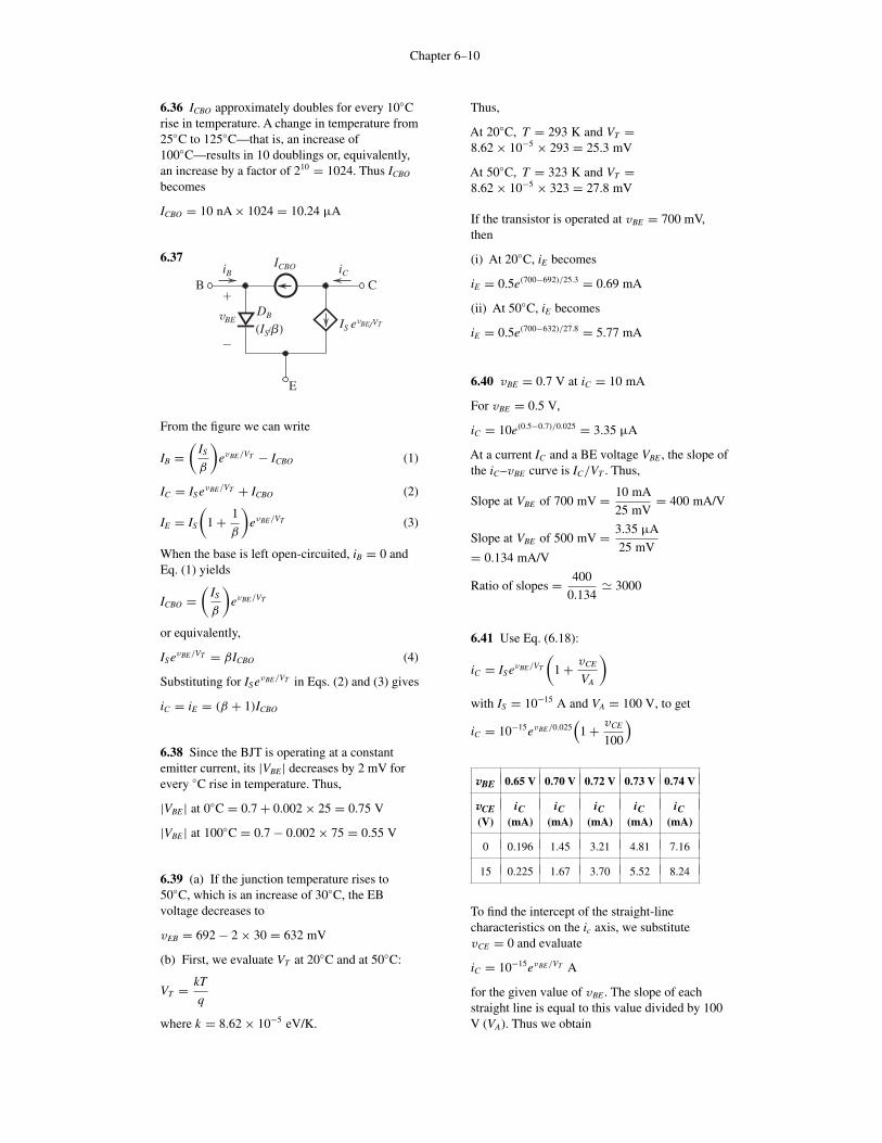
6.37
From the figure we can write
IB =(
IS
β
)evBE/VT − ICBO (1)
IC = ISevBE/VT + ICBO (2)
IE = IS
(1 + 1
β
)evBE/VT (3)
When the base is left open-circuited, iB = 0 andEq. (1) yields
ICBO =(
IS
β
)evBE/VT
or equivalently,
ISevBE/VT = βICBO (4)
Substituting for ISevBE/VT in Eqs. (2) and (3) gives
iC = iE = (β + 1)ICBO
6.38 Since the BJT is operating at a constantemitter current, its |VBE | decreases by 2 mV forevery ◦C rise in temperature. Thus,
|VBE | at 0◦C = 0.7 + 0.002 × 25 = 0.75 V
|VBE | at 100◦C = 0.7 − 0.002 × 75 = 0.55 V
6.39 (a) If the junction temperature rises to50◦C, which is an increase of 30◦C, the EBvoltage decreases to
vEB = 692 − 2 × 30 = 632 mV
(b) First, we evaluate VT at 20◦C and at 50◦C:
VT = kT
q
where k = 8.62 × 10⁻⁵ eV/K.
Thus,
At 20◦C, T = 293 K and VT =8.62 × 10−5 × 293 = 25.3 mV
At 50◦C, T = 323 K and VT =8.62 × 10−5 × 323 = 27.8 mV
If the transistor is operated at vBE = 700 mV,then
(i) At 20◦C, iE becomes
iE = 0.5e(700−692)/25.3 = 0.69 mA
(ii) At 50◦C, iE becomes
iE = 0.5e(700−632)/27.8 = 5.77 mA
6.40 vBE = 0.7 V at iC = 10 mA
For vBE = 0.5 V,
iC = 10e(0.5−0.7)/0.025 = 3.35 μA
At a current IC and a BE voltage VBE , the slope ofthe iC–vBE curve is IC/VT . Thus,
Slope at VBE of 700 mV = 10 mA
25 mV= 400 mA/V
Slope at VBE of 500 mV = 3.35 μA
25 mV= 0.134 mA/V
Ratio of slopes = 400
0.134� 3000
6.41 Use Eq. (6.18):
iC = ISevBE/VT
(1 + vCE
VA
)
with IS = 10−15 A and VA = 100 V, to get
iC = 10−15evBE/0.025(
1 + vCE
100
)
vBE 0.65 V 0.70 V 0.72 V 0.73 V 0.74 V
vCE iC iC iC iC iC(V) (mA) (mA) (mA) (mA) (mA)
0 0.196 1.45 3.21 4.81 7.16
15 0.225 1.67 3.70 5.52 8.24
To find the intercept of the straight-linecharacteristics on the ic axis, we substitutevCE = 0 and evaluate
iC = 10−15evBE/VT A
for the given value of vBE . The slope of eachstraight line is equal to this value divided by 100V (VA). Thus we obtain
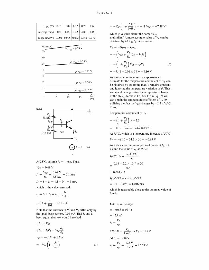
Chapter 6–11
vBE (V) 0.65 0.70 0.72 0.73 0.74
Intercept (mA) 0.2 1.45 3.22 4.80 7.16
Slope (mA/V) 0.002 0.015 0.032 0.048 0.072
6.42
I � 1.1 mA
6.8 k�
68 k�
�
�
VBE IE
IB
VE
R2
R1
I2
I1
At 25◦C, assume IE = 1 mA. Thus,
VBE = 0.68 V
I1 = VBE
R1= 0.68 V
6.8 k�= 0.1 mA
IE = I − I1 = 1.1 − 0.1 = 1 mA
which is the value assumed.
I2 = I1 + IB = I1 + IE
β + 1
= 0.1 + 1
101= 0.11 mA
Note that the currents in R1 and R2 differ only bythe small base current, 0.01 mA. Had I1 and I2
been equal, then we would have had
I1R1 = VBE
I2R2 � I1R2 = VBER2
R1
VE = −(I1R1 + I2R2)
= −VBE
(1 + R2
R1
)(1)
= −VBE
(1 + 6.8
0.68
)= −11 VBE = −7.48 V
which gives this circuit the name “VBE
multiplier.” A more accurate value of VE can beobtained by taking IB into account:
VE = −(I1R1 + I2R2)
= −(
VBE + R2
R1VBE + IBR2
)
= −(
1 + R2
R1
)VBE − IBR2 (2)
= −7.48 − 0.01 × 68 = −8.16 V
As temperature increases, an approximateestimate for the temperature coefficient of VE canbe obtained by assuming that IE remains constantand ignoring the temperature variation of β. Thus,we would be neglecting the temperature changeof the (IBR2) terms in Eq. (2). From Eq. (2) wecan obtain the temperature coefficient of VE byutilizing the fact the VBE changes by – 2.2 mV/◦C.Thus,
Temperature coefficient of VE
= −(
1 + R2
R1
)× −2.2
= −11 × −2.2 = +24.2 mV/◦C
At 75◦C, which is a temperature increase of 50◦C,
VE = −8.16 + 24.2 × 50 = −6.95 V
As a check on our assumption of constant IE , letus find the value of IE at 75◦C:
I1(75◦C) = VBE(75◦C)
R1
= 0.68 − 2.2 × 10−3 × 50
6.8
= 0.084 mA
IE(75◦C) = I − I1(75◦C)
= 1.1 − 0.084 = 1.016 mA
which is reasonably close to the assumed value of1 mA.
6.43 ro = 1/slope
= 1/(0.8 × 10−5)
= 125 k�
ro = VA
IC
125 k� = VA
1 mA⇒ VA = 125 V
At IC = 10 mA,
ro = VA
IC= 125 V
10 mA= 12.5 k�

Chapter 6–12
6.44 ro = VA
IC= 50 V
IC
Thus,
At IC = 1 mA, ro = 50 V
1 mA= 50 k�
At IC = 100 μA, ro = 50 V
0.1 mA= 500 k�
6.45
0.3
1.1
1.3
0 5 10 15�VA vCE (V)
iC (mA)
Slope of iC–vCE line corresponding tovBE = 710 mV is
Slope = 1.3 − 1.1
15 − 5= 0.2 mA
10 V= 0.02 mA/V
Near saturation, VCE = 0.3 V, thus
iC = 1.1 − 0.02 × (5 − 0.3)
= 1.006 � 1 mA
iC will be 1.2 mA at,
vCE = 5 + 1.2 − 1.1
0.02= 10 V
The intercept of the iC–vCE straight line on the iC
axis will be at
iC = 1.1 − 5 × 0.02 = 1 mA
Thus, the Early voltage is obtained as
Slope = iC(at vCE = 0)
VA
⇒ VA = 1
0.02= 50 V
ro = VA
IC= 50 V
1 mA= 50 k�
which is the inverse of the slope of the iC–vCE
line.
6.46 The equivalent circuits shown in the figurecorrespond to the circuits in Fig. 6.19.
(b)
B C
E
vEB(IS/b)
biB
iB
DB
�
�
iE
iC
ro
6.47 β = iC
iB= 1 mA
10 μA= 100
βac = �iC
�iB
∣∣∣∣vCE constant
= 0.08 mA
1.0 μA= 80
�iC = �iB × βac + �vCE
ro
where
ro = VA
IC= 100
1= 100 k�
Thus,
�iC = 2 × 80 + 2
100× 103 = 180 μA
= 0.18 mA
6.48 Refer to the circuit in Fig. P6.48.
(a) For active-mode operation with VC = 2 V:
IC = VCC − VC
RC= 10 − 2
1= 8 mA
IB = IC
β= 8
50= 0.16 mA
VBB = IBRB + VBE
= 0.16 × 10 + 0.7 = 2.3 V
(b) For operation at the edge of saturation:
VCE = 0.3 V
IC = VCC − VCE
RC= 10 − 0.3
1= 9.7 mA
Chapter 6–13
IB = IC
β= 9.7
50= 0.194 mA
VBB = IBRB + VBE
= 0.194 × 10 + 0.7 = 2.64 V
(c) For operation deep in saturation withβforced = 10:
VCE = 0.2 V
IC = VCC − VCE
RC= 10 − 0.2
1= 9.8 mA
IB = IC
βforced= 9.8
10= 0.98 mA
VBB = IBRB + VBE
= 0.98 × 10 + 0.7 = 10.5 V
6.49 Refer to the circuit in Fig. P6.48 (withVBB = VCC) and to the BJT equivalent circuit ofFig. 6.21.
IC = VCC − 0.2
RC
IB = VCC − 0.7
RB
βforced ≡ IC
IB
Thus,
βforced =(
VCC − 0.2
VCC − 0.7
) (RB
RC
)(1)
Pdissipated = VCC(IC + IB)
= VCC(βforcedIB + IB)
= (βforced + 1)VCCIB (2)
For VCC = 5 V and βforced = 10 andPdissipated ≤ 20 mW, we can proceed as follows.
Using Eq. (1) we can determine (RB/RC):
10 =(
5 − 0.2
5 − 0.7
) (RB
RC
)
⇒ RB
RC= 8.96 (3)
Using Eq. (2), we can find IB:
(10 + 1) × 5 × IB ≤ 20 mW
⇒ IB ≤ 0.36 mA
Thus,
VCC − 0.7
RB≤ 0.36 mA
⇒ RB ≥ 11.9 k�
From the table of 1% resistors in Appendix J weselect
RB = 12.1 k�
Substituting in Eq. (3), we have
RC = 1.35 k�
From the table of 1% resistors in Appendix J weselect
RC = 1.37 k�
For these values:
IC = 5 − 0.2
1.37= 3.5 mA
IB = 5 − 0.7
12.1= 0.36 mA
Thus,
βforced = 3.5
0.36= 9.7
Pdissipated = VCC(IC + IB)
= 5 × 3.86 = 19.2 mW
6.50�5 V
VB � �4.3 V �
�
IB
IC
RB � 10 k�
1 k�
VECsat � 0.2 V
VC � �4.8 V
Assume saturation-mode operation. From thefigure we see that
IC = VC
1 k�= 4.8
1= 4.8 mA
IB = VB
RB= 4.3
10= 0.43 mA
Thus,
βforced ≡ IC
IB= 4.8
0.43= 11.2
Since 11.2 is lower than the transistor β of 50, wehave verified that the transistor is operating insaturation, as assumed.
VC = VCC − VECsat = 5 − 0.2 = 4.8 V
To operate at the edge of saturation,
VEC = 0.3 V and IC/IB = β = 50
Chapter 6–14
Thus,
IC = 5 − 0.3
1= 4.7 mA
IB = IC
β= 4.7
50= 0.094 mA
RB = 4.3
IB= 4.3
0.094= 45.7 k�
6.51
(a)
�3 V
1 k� IC IE � 1.3 mA
VE � � 2 � 0.7 � 1.3 V
�2 V
1 k� IE � � 1.3 mA1.31
VC � 3 � 1.3 � 1 � �1.7 V
3
4
1
2
(b)
�3 V
1 k� IC IE � 1 mA
�1.7 V
1 k� IE �
�1 mA
1.01
VC � 3 � 1 � 1 � �2 V
3
4
2
VE � �1.0 V 1
(c)
�3 V
1 k�0
VE � 0 V
0 V
1 k�
0
VC � 3 � 0 � 3 V 4
3
2
1
The analysis and the results are given on thecircuit diagrams of Figs. 1 through 3. The circlednumbers indicate the order of the analysis steps.
6.52
�3 V
�
1 k�
VB � 0.7
VB
1 k�
�VC � VB � 0.4
VCE � 0.3 V
3 � (VB � 0.4)1
IC �
VB � 0.71
IE �
Figure 1
Figure 1 shows the circuit with the value of VB
that results in operation at the edge of saturation.Since β is very high,
IC � IE
3 − (VB − 0.4)
1= VB − 0.7
1
⇒ VB = 2.05 V
�3 V
�
1 k�
�VB � 0.7
VB
1 k�
VB � 0.5
VCEsat � 0.2 V
IC
IB
IE
Figure 2
Figure 2 shows the circuit with the value of VB
that results in the transistor operating insaturation, with
IE = VB − 0.7
1= VB − 0.7
IC = 3 − (VB − 0.5)
1= 3.5 − VB
IB = IE − IC = 2VB − 4.2
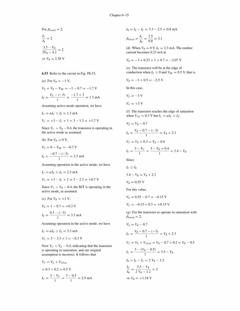
Chapter 6–15
For βforced = 2,
IC
IB= 2
3.5 − VB
2VB − 4.2= 2
⇒ VB = 2.38 V
6.53 Refer to the circuit in Fig. P6.53.
(a) For VB = −1 V,
VE = VB − VBE = −1 − 0.7 = −1.7 V
IE = VE − (−3)
1= −1.7 + 3
1= 1.3 mA
Assuming active-mode operation, we have
IC = αIE � IE = 1.3 mA
VC = +3 − IC × 1 = 3 − 1.3 = +1.7 V
Since VC > VB − 0.4, the transistor is operating inthe active mode as assumed.
(b) For VB = 0 V,
VE = 0 − VBE = −0.7 V
IE = −0.7 − (−3)
1= 2.3 mA
Assuming operation in the active mode, we have
IC = αIE � IE = 2.3 mA
VC = +3 − IC × 1 = 3 − 2.3 = +0.7 V
Since VC > VB − 0.4, the BJT is operating in theactive mode, as assumed.
(c) For VB = +1 V,
VE = 1 − 0.7 = +0.3 V
IE = 0.3 − (−3)
1= 3.3 mA
Assuming operation in the active mode, we have
IC = αIE � IE = 3.3 mA
VC = 3 − 3.3 × 1 = −0.3 V
Now VC < VB − 0.4, indicating that the transistoris operating in saturation, and our originalassumption is incorrect. It follows that
VC = VE + VCEsat
= 0.3 + 0.2 = 0.5 V
IC = 3 − VC
1= 3 − 0.5
1= 2.5 mA
IB = IE − IC = 3.3 − 2.5 = 0.8 mA
βforced = IC
IB= 2.5
0.8= 3.1
(d) When VB = 0 V, IE = 2.3 mA. The emittercurrent becomes 0.23 mA at
VB = −3 + 0.23 × 1 + 0.7 = −2.07 V
(e) The transistor will be at the edge ofconduction when IE � 0 and VBE = 0.5 V, that is,
VB = −3 + 0.5 = −2.5 V
In this case,
VE = −3 V
VC = +3 V
(f) The transistor reaches the edge of saturationwhen VCE = 0.3 V but IC = αIE � IE :
VE = VB − 0.7
IE = VB − 0.7 − (−3)
1= VB + 2.3
VC = VE + 0.3 = VB − 0.4
IC = 3 − VC
1= 3 − VB + 0.4
1= 3.4 − VB
Since
IC � IE
3.4 − VB = VB + 2.3
VB = 0.55 V
For this value,
VE = 0.55 − 0.7 = −0.15 V
VC = −0.15 + 0.3 = +0.15 V
(g) For the transistor to operate in saturation withβforced = 2,
VE = VB − 0.7
IE = VB − 0.7 − (−3)
1= VB + 2.3
VC = VE + VCEsat = VB − 0.7 + 0.2 = VB − 0.5
IC = 3 − (VB − 0.5)
1= 3.5 − VB
IB = IE − IC = 2 VB − 1.2
IC
IB= 3.5 − VB
2 VB − 1.2= 2
⇒ VB = +1.18 V
Chapter 6–16
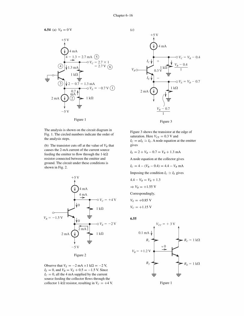
6.54 (a) VB = 0 V
�5 V
�5 V
4 � 1.3 � 2.7 mA
2 � 0.7 � 1.3 mA
4 mA
1.3 mA
2 mA
0.7mA
1 k�
1 k�
VC � 2.7 � 1� 2.7 V
VE � �0.7 V
5
6
1
2
3
4
Figure 1
The analysis is shown on the circuit diagram inFig. 1. The circled numbers indicate the order ofthe analysis steps.
(b) The transistor cuts off at the value of VB thatcauses the 2-mA current of the current sourcefeeding the emitter to flow through the 1-k�
resistor connected between the emitter andground. The circuit under these conditions isshown in Fig. 2.
�5 V
�5 V
4 mA
4 mA
0
0
2 mA
2 mA1 k�
1 k�
VC � �4 V
VE � �2 V
VB � �1.5 V
Figure 2
Observe that VE = −2 mA ×1 k� = −2 V,IE = 0, and VB = VE + 0.5 = −1.5 V. SinceIC = 0, all the 4 mA supplied by the currentsource feeding the collector flows through thecollector 1-k� resistor, resulting in VC = +4 V.
(c)
�5 V
1
4 mA
0.3 V
2 mA1 k�
1 k�
�
�
VC � VB � 0.4
VB � 0.4IC
IE
VB
VE � VB � 0.7
1VB � 0.7
Figure 3
Figure 3 shows the transistor at the edge ofsaturation. Here VCE = 0.3 V andIC = αIE � IE . A node equation at the emittergives
IE = 2 + VB − 0.7 = VB + 1.3 mA
A node equation at the collector gives
IC = 4 − (VB − 0.4) = 4.4 − VB mA
Imposing the condition IC � IE gives
4.4 − VB = VB + 1.3
⇒ VB = +1.55 V
Correspondingly,
VE = +0.85 V
VC = +1.15 V
6.55
0.1 mA
VB � �1.2 V
R2
VCC � � 3 V
RC � 1 k�R1
RE � 1 k�
0
Figure 1
Chapter 6–17
From Fig. 1 we see that
R1 + R2 = VCC
0.1 mA= 3
0.1= 30 k�
VCCR2
R1 + R2= 1.2
3 × R2
30= 1.2
⇒ R2 = 12 k�
R1 = 30 − 12 = 18 k�
For β = 100, to obtain the collector current, wereplace the voltage divider with its Théveninequivalent, consisting of
VBB = 3 × R2
R1 + R2= 3 × 12
18 + 12= 1.2 V
RB = R1 ‖ R2 = 12 ‖ 18 = 7.2 k�
�3 V
VBB
IB
IC
IE
RB
RE � 1 k�
RC � 1 k�
VC
Figure 2
Refer to Fig. 2. Assuming active-mode operation,we can write a loop equation for the base–emitterloop:
VBB = IBRB + VBE + IERE
1.2 = IE
β + 1× 7.2 + 0.7 + IE × 1
⇒ IE = 1.2 − 0.7
1 + 7.2
101
= 0.47 mA
IC = αIE = 0.99 × 0.47 = 0.46 mA
VC = +3 − 0.46 × 1 = +2.54 V
Since VB = IERE + VBE = 0.47 + 0.7 = 1.17 V,we see that VC > VB − 0.4, and thus the transistoris operating in the active region, as assumed.
6.56 Refer to the circuit in Fig. P6.56.
VE = 1 V
IE = 3 − 1
5= 0.4 mA
VB = VE − 0.7 = 0.3 V
IB = VB
50 k�= 0.3
50= 0.006 mA
IC = IE − IB = 0.4 − 0.006 = 0.394 mA
VC = −3 + 5 × 0.394 = −1.03 V
Observe that VC < VB, confirming our implicitassumption that the transistor is operating in theactive region.
β = IC
IB= 0.394
0.006= 66
α = IC
IE= 0.394
0.4= 0.985
6.57�3 V
�3 V
IE
IC
�
�
VBC � 1 V
VE � �0.7 V
VC � �1 V
RE
RC
Refer to the figure. To obtain IE = 0.5 mA weselect RE according to
RE = 3 − 0.7
0.5= 4.6 k�
To obtain VC = −1 V, we select RC according to
RC = −1 − (−3)
0.5= 4 k�
where we have utilized the fact that α � 1 andthus IC � IE = 0.5 mA. From the table of 5%resistors in Appendix J we select
RE = 4.7 k� and RC = 3.9 k�
For these values,
IE = 3 − 0.7
4.7= 0.49 mA
IC � IE = 0.49 mA
VBC = 0 − VC = −(−3 + 0.49 × 3.9) = −1.1 V
Chapter 6–18
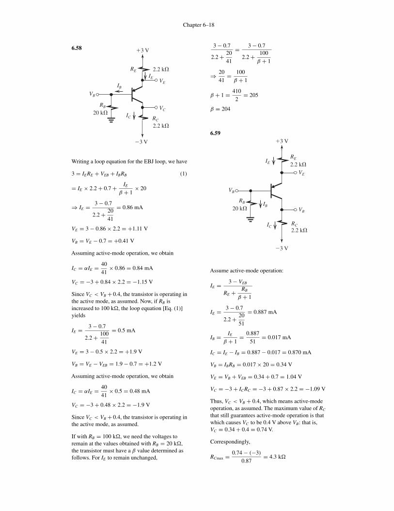
6.58 �3 V
�3 V
IE
IC
VE
VC
RE 2.2 k�
2.2 k�
20 k�RC
RB
VB
IB
Writing a loop equation for the EBJ loop, we have
3 = IERE + VEB + IBRB (1)
= IE × 2.2 + 0.7 + IE
β + 1× 20
⇒ IE = 3 − 0.7
2.2 + 20
41
= 0.86 mA
VE = 3 − 0.86 × 2.2 = +1.11 V
VB = VE − 0.7 = +0.41 V
Assuming active-mode operation, we obtain
IC = αIE = 40
41× 0.86 = 0.84 mA
VC = −3 + 0.84 × 2.2 = −1.15 V
Since VC < VB + 0.4, the transistor is operating inthe active mode, as assumed. Now, if RB isincreased to 100 k�, the loop equation [Eq. (1)]yields
IE = 3 − 0.7
2.2 + 100
41
= 0.5 mA
VE = 3 − 0.5 × 2.2 = +1.9 V
VB = VE − VEB = 1.9 − 0.7 = +1.2 V
Assuming active-mode operation, we obtain
IC = αIE = 40
41× 0.5 = 0.48 mA
VC = −3 + 0.48 × 2.2 = −1.9 V
Since VC < VB + 0.4, the transistor is operating inthe active mode, as assumed.
If with RB = 100 k�, we need the voltages toremain at the values obtained with RB = 20 k�,the transistor must have a β value determined asfollows. For IE to remain unchanged,
3 − 0.7
2.2 + 20
41
= 3 − 0.7
2.2 + 100
β + 1
⇒ 20
41= 100
β + 1
β + 1 = 410
2= 205
β = 204
6.59�3 V
�3 V
IE
IC
VE
VB
RE
2.2 k�
2.2 k�
20 k�
RC
RB
VB
IB
Assume active-mode operation:
IE = 3 − VEB
RE + RB
β + 1
IE = 3 − 0.7
2.2 + 20
51
= 0.887 mA
IB = IE
β + 1= 0.887
51= 0.017 mA
IC = IE − IB = 0.887 − 0.017 = 0.870 mA
VB = IBRB = 0.017 × 20 = 0.34 V
VE = VB + VEB = 0.34 + 0.7 = 1.04 V
VC = −3 + ICRC = −3 + 0.87 × 2.2 = −1.09 V
Thus, VC < VB + 0.4, which means active-modeoperation, as assumed. The maximum value of RC
that still guarantees active-mode operation is thatwhich causes VC to be 0.4 V above VB: that is,VC = 0.34 + 0.4 = 0.74 V.
Correspondingly,
RCmax = 0.74 − (−3)
0.87= 4.3 k�
Chapter 6–19
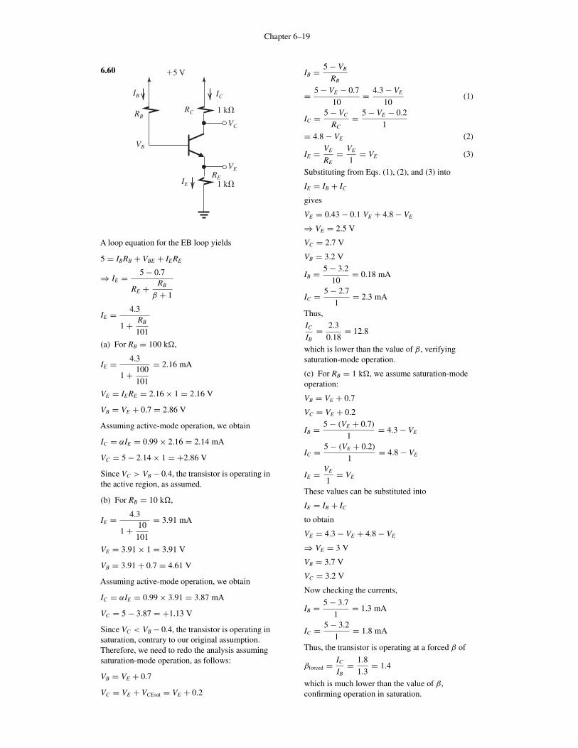
6.60
1 k�
1 k�
�5 V
REIE
ICIB
RBRC
VB
VC
VE
A loop equation for the EB loop yields
5 = IBRB + VBE + IERE
⇒ IE = 5 − 0.7
RE + RB
β + 1
IE = 4.3
1 + RB
101
(a) For RB = 100 k�,
IE = 4.3
1 + 100
101
= 2.16 mA
VE = IERE = 2.16 × 1 = 2.16 V
VB = VE + 0.7 = 2.86 V
Assuming active-mode operation, we obtain
IC = αIE = 0.99 × 2.16 = 2.14 mA
VC = 5 − 2.14 × 1 = +2.86 V
Since VC > VB − 0.4, the transistor is operating inthe active region, as assumed.
(b) For RB = 10 k�,
IE = 4.3
1 + 10
101
= 3.91 mA
VE = 3.91 × 1 = 3.91 V
VB = 3.91 + 0.7 = 4.61 V
Assuming active-mode operation, we obtain
IC = αIE = 0.99 × 3.91 = 3.87 mA
VC = 5 − 3.87 = +1.13 V
Since VC < VB − 0.4, the transistor is operating insaturation, contrary to our original assumption.Therefore, we need to redo the analysis assumingsaturation-mode operation, as follows:
VB = VE + 0.7
VC = VE + VCEsat = VE + 0.2
IB = 5 − VB
RB
= 5 − VE − 0.7
10= 4.3 − VE
10(1)
IC = 5 − VC
RC= 5 − VE − 0.2
1= 4.8 − VE (2)
IE = VE
RE= VE
1= VE (3)
Substituting from Eqs. (1), (2), and (3) into
IE = IB + IC
gives
VE = 0.43 − 0.1 VE + 4.8 − VE
⇒ VE = 2.5 V
VC = 2.7 V
VB = 3.2 V
IB = 5 − 3.2
10= 0.18 mA
IC = 5 − 2.7
1= 2.3 mA
Thus,
IC
IB= 2.3
0.18= 12.8
which is lower than the value of β, verifyingsaturation-mode operation.
(c) For RB = 1 k�, we assume saturation-modeoperation:
VB = VE + 0.7
VC = VE + 0.2
IB = 5 − (VE + 0.7)
1= 4.3 − VE
IC = 5 − (VE + 0.2)
1= 4.8 − VE
IE = VE
1= VE
These values can be substituted into
IE = IB + IC
to obtain
VE = 4.3 − VE + 4.8 − VE
⇒ VE = 3 V
VB = 3.7 V
VC = 3.2 V
Now checking the currents,
IB = 5 − 3.7
1= 1.3 mA
IC = 5 − 3.2
1= 1.8 mA
Thus, the transistor is operating at a forced β of
βforced = IC
IB= 1.8
1.3= 1.4
which is much lower than the value of β,confirming operation in saturation.
Chapter 6–20
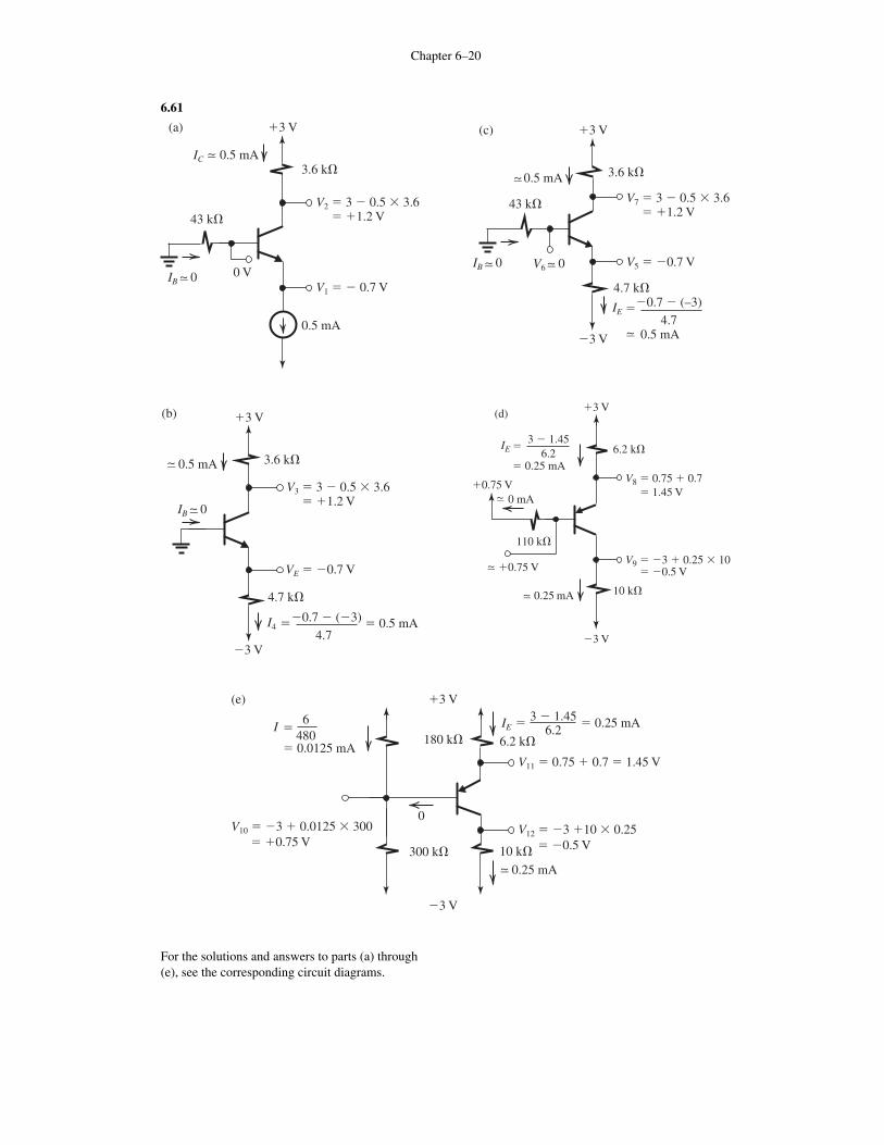
6.61
�3 V(a)
0 VIB 0
IC 0.5 mA
V2 � 3 � 0.5 � 3.6� �1.2 V
V1 � � 0.7 V
3.6 k�
43 k�
0.5 mA
�3 V(b)
�3 V
IB 0~�
~�0.5 mA
I4 � � 0.5 mA�0.7 � (�3)4.7
V3 � 3 � 0.5 � 3.6� �1.2 V
VE � �0.7 V
3.6 k�
4.7 k�
0.25 mA
I �6
480� 0.0125 mA
�3 V(e)
�3 V
V11 � 0.75 � 0.7 � 1.45 V
V12 � �3 �10 � 0.25 � �0.5 V
V10 � �3 � 0.0125 � 300 � �0.75 V
6.2 k�180 k�
300 k�
0
10 k�
3 � 1.456.2
IE � � 0.25 mA
For the solutions and answers to parts (a) through(e), see the corresponding circuit diagrams.
0.5 mA
IE �
0.5 mA
�0.7 � (–3)4.7
�3 V
�3 V
(c)
IB 0 V6 0
V7 � 3 � 0.5 � 3.6� �1.2 V
V5 � �0.7 V
3.6 k�
43 k�
4.7 k�
IE �
0 mA
3 � 1.456.2
� 0.25 mA
�3 V
�3 V
(d)
~�
�0.75 V
V8 � 0.75 � 0.7�0.75 V
� 1.45 V
V9 � �3 � 0.25 � 10 � �0.5 V
6.2 k�
10 k�
110 k�
0.25 mA
Chapter 6–21
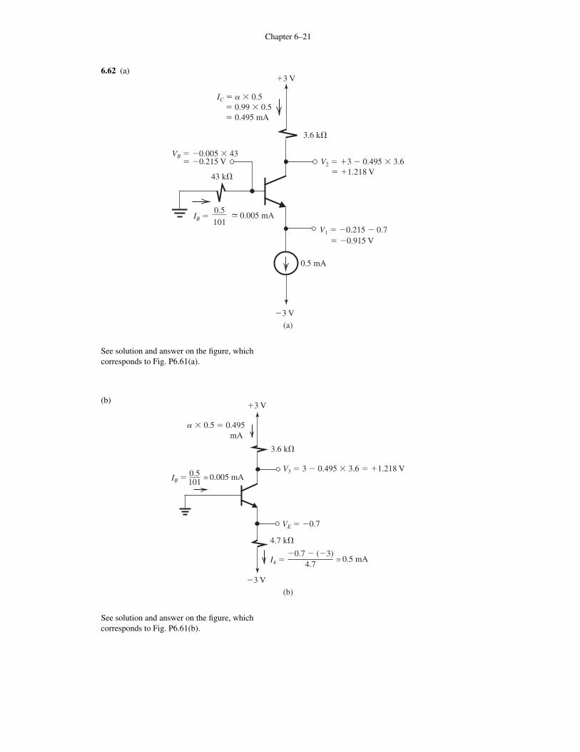
6.62 (a)�3 V
�3 V
43 k�
3.6 k�
V2 � �3 � 0.495 � 3.6
0.5 mA
V1 � �0.215 � 0.7
IC � a � 0.5 � 0.99 � 0.5 � 0.495 mA
VB � �0.005 � 43
0.5101
IB � 0.005 mA
� �1.218 V
� �0.915 V
� �0.215 V
(a)
See solution and answer on the figure, whichcorresponds to Fig. P6.61(a).
(b)
(b)
�3 V
�3 V
3.6 k�
V3 � 3 � 0.495 � 3.6 � �1.218 V
4.7 k�
0.5101
VE � �0.7
a � 0.5 � 0.495mA
IB � 0.005 mA
�0.7 � (�3)4.7I4 � 0.5 mA
See solution and answer on the figure, whichcorresponds to Fig. P6.61(b).
a
Chapter 6–22
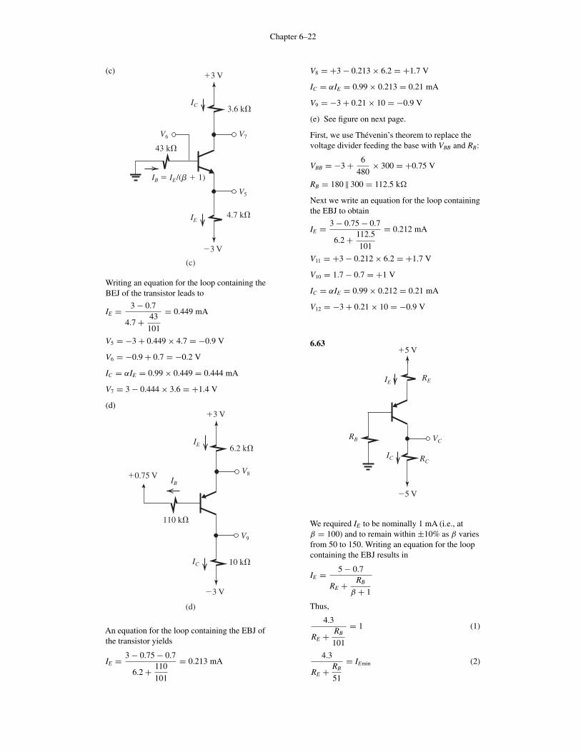
(c)
(c)
�3 V
�3 V
43 k�
3.6 k�
V7
4.7 k�
V5
IC
IE
IB � IE/(b � 1)
V6
Writing an equation for the loop containing theBEJ of the transistor leads to
IE = 3 − 0.7
4.7 + 43
101
= 0.449 mA
V5 = −3 + 0.449 × 4.7 = −0.9 V
V6 = −0.9 + 0.7 = −0.2 V
IC = αIE = 0.99 × 0.449 = 0.444 mA
V7 = 3 − 0.444 × 3.6 = +1.4 V
(d)
(d)
�3 V
�0.75 V
�3 V
6.2 k�
V8
10 k�
110 k�
V9
IE
IB
IC
An equation for the loop containing the EBJ ofthe transistor yields
IE = 3 − 0.75 − 0.7
6.2 + 110
101
= 0.213 mA
V8 = +3 − 0.213 × 6.2 = +1.7 V
IC = αIE = 0.99 × 0.213 = 0.21 mA
V9 = −3 + 0.21 × 10 = −0.9 V
(e) See figure on next page.
First, we use Thévenin’s theorem to replace thevoltage divider feeding the base with VBB and RB:
VBB = −3 + 6
480× 300 = +0.75 V
RB = 180 ‖ 300 = 112.5 k�
Next we write an equation for the loop containingthe EBJ to obtain
IE = 3 − 0.75 − 0.7
6.2 + 112.5
101
= 0.212 mA
V11 = +3 − 0.212 × 6.2 = +1.7 V
V10 = 1.7 − 0.7 = +1 V
IC = αIE = 0.99 × 0.212 = 0.21 mA
V12 = −3 + 0.21 × 10 = −0.9 V
6.63
IC
�5 V
�5 V
RB
IE
VC
RE
RC
We required IE to be nominally 1 mA (i.e., atβ = 100) and to remain within ±10% as β variesfrom 50 to 150. Writing an equation for the loopcontaining the EBJ results in
IE = 5 − 0.7
RE + RB
β + 1
Thus,
4.3
RE + RB
101
= 1 (1)
4.3
RE + RB
51
= IEmin (2)

Chapter 6–23
This figure belongs to Problem 6.62, part (e).
(e)
IE
IC IC
IBIB
�3 V
��
�3 V
V11
V12
V10
6.2 k�180 k�
300 k� 10 k�
�3 V
�3 V
RB
VBB
V10
IE
V11
V12
6.2 k�
10 k�
4.3
RE + RB
151
= IEmax (3)
If we set IEmin = 0.9 mA and solve Eqs. (1) and(2) simultaneously, we obtain
RE = 3.81 k�
RB = 49.2 k�
Substituting theses values in Eqs. (2) and (3) gives
IEmin = 0.9 mA
IEmax = 1.04 mA
Obviously, this is an acceptable design.Alternatively, if we set IEmax in Eq. (3) to 1.1 mAand solve Eqs. (1) and (3) simultaneously, weobtain
RE = 3.1 k�
RB = 119.2 k�
Substituting these values in Eqs. (2) and (3) gives
IEmin = 0.8 mA
IEmax = 1.1 mA
Obviously this is not an acceptable design (IEmin
is 20% lower than nominal).
Therefore, we shall use the first design.Specifying the resistor values to the nearestkilohm results in
RE = 4 k�
RB = 50 k�
To obtain the value of RC , we note that at thenominal emitter current value of 1 mA,VC = −1 V,
IC = αIE = 0.99 mA
RC = −1 − (−5)
0.99= 4.04 k�
Specified to the nearest kilohm,
RC = 4 k�
Finally, for our design we need to determine therange obtained for collector current and collectorvoltage for β ranging from 50 to 150 with anominal value of 100. We compute the nominalvalue of IE from
IEnominal = 4.3
4 + 50
101
= 0.96 mA
We utilize Eqs. (2) and (3) to compute IEmin andIEmax,
IEmin = 4.3
4 + 50
51
= 0.86 mA
IEmax = 4.3
4 + 50
151
= 0.99 mA
Thus,
IEmax
IEnominal= 0.99
0.96= 1.03
IEmin
IEnominal= 0.86
0.96= 0.9
which meet our specifications. The collectorcurrents are
ICnominal = 0.99 × 0.96 = 0.95 mA
ICmin = 0.99 × 0.86 = 0.85 mA
ICmax = 0.99 × 0.99 = 0.98 mA
and the collector voltages are
VCnominal = −5 + 0.95 × 4 = −1.2 V
VCmin = −5 + 0.85 × 4 = −1.6 V
VCmax = −5 + 0.98 × 4 = −1.1 V
Chapter 6–24
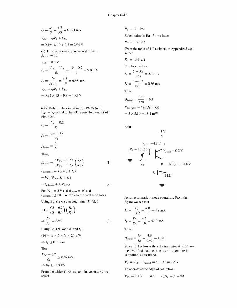
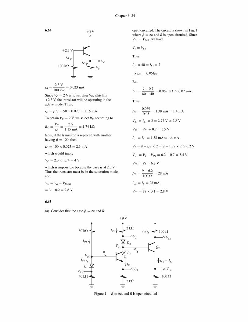
6.64
IC
IB
�3 V
�2.3 V
100 k�
VC
RC
IB = 2.3 V
100 k�= 0.023 mA
Since VC = 2 V is lower than VB, which is+2.3 V, the transistor will be operating in theactive mode. Thus,
IC = βIB = 50 × 0.023 = 1.15 mA
To obtain VC = 2 V, we select RC according to
RC = VC
IC= 2 V
1.15 mA= 1.74 k�
Now, if the transistor is replaced with anotherhaving β = 100, then
IC = 100 × 0.023 = 2.3 mA
which would imply
VC = 2.3 × 1.74 = 4 V
which is impossible because the base is at 2.3 V.Thus the transistor must be in the saturation modeand
VC = VE − VECsat
= 3 − 0.2 = 2.8 V
6.65
(a) Consider first the case β = ∞ and R
�9 V
80 k� 100 �
100 �
2 k�
2 k�
40 k�
ID1
IC1
IE1
VE1
VE2
IE2
VC2
IC1VB1 Q1
Q2VC1
D1
ID1
D2
V1
V2
IC2 � IE2
0 0
Figure 1 β = ∞, and R is open circuited
open circuited. The circuit is shown in Fig. 1,where β = ∞ and R is open circuited. SinceVD1 = VBE1, we have
V1 = VE1
Thus,
ID1 × 40 = IE1 × 2
⇒ ID1 = 0.05IE1
But
ID1 = 9 − 0.7
80 + 40= 0.069 mA � 0.07 mA
Thus,
IE1 = 0.069
0.05= 1.38 mA � 1.4 mA
VE1 = IE1 × 2 = 2.77 V � 2.8 V
VB1 = VE1 + 0.7 = 3.5 V
IC1 = IE1 = 1.38 mA � 1.4 mA
V2 = 9 − IC1 × 2 = 9 − 1.38 × 2 � 6.2 V
VC1 = V2 − VD2 = 6.2 − 0.7 = 5.5 V
VE2 = V2 = 6.2 V
IE2 = 9 − 6.2
100 �= 28 mA
IC2 = IE = 28 mA
VC2 = 28 × 0.1 = 2.8 V
Chapter 6–25
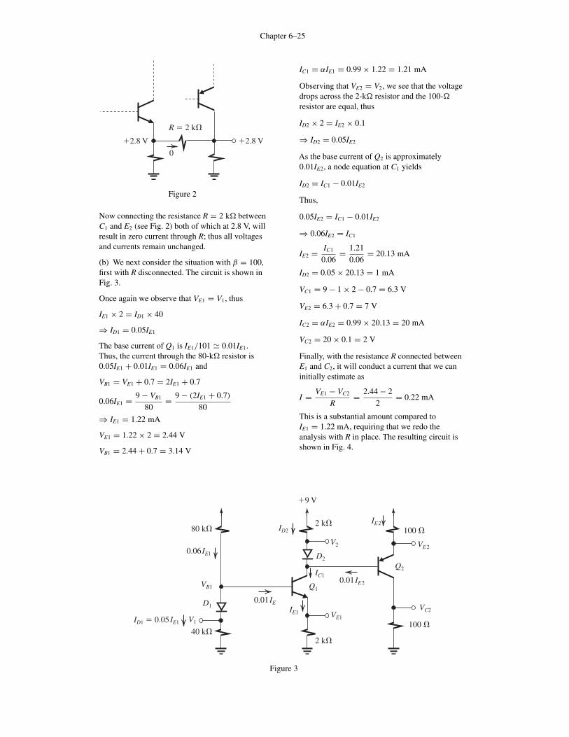
�2.8 V �2.8 V
0
R � 2 k�
Figure 2
Now connecting the resistance R = 2 k� betweenC1 and E2 (see Fig. 2) both of which at 2.8 V, willresult in zero current through R; thus all voltagesand currents remain unchanged.
(b) We next consider the situation with β = 100,first with R disconnected. The circuit is shown inFig. 3.
Once again we observe that VE1 = V1, thus
IE1 × 2 = ID1 × 40
⇒ ID1 = 0.05IE1
The base current of Q1 is IE1/101 � 0.01IE1.Thus, the current through the 80-k� resistor is0.05IE1 + 0.01IE1 = 0.06IE1 and
VB1 = VE1 + 0.7 = 2IE1 + 0.7
0.06IE1 = 9 − VB1
80= 9 − (2IE1 + 0.7)
80
⇒ IE1 = 1.22 mA
VE1 = 1.22 × 2 = 2.44 V
VB1 = 2.44 + 0.7 = 3.14 V
�9 V
80 k� 100 �
100 �
2 k�
2 k�
0.01IE
0.01 IE2
40 k�
ID1 � 0.05 IE1
ID2
IE1 VE1
VE2
IE2
VC2
IC1
VB1 Q1
Q2
D1
D2
V1
V20.06 IE1
Figure 3
IC1 = αIE1 = 0.99 × 1.22 = 1.21 mA
Observing that VE2 = V2, we see that the voltagedrops across the 2-k� resistor and the 100-�resistor are equal, thus
ID2 × 2 = IE2 × 0.1
⇒ ID2 = 0.05IE2
As the base current of Q2 is approximately0.01IE2, a node equation at C1 yields
ID2 = IC1 − 0.01IE2
Thus,
0.05IE2 = IC1 − 0.01IE2
⇒ 0.06IE2 = IC1
IE2 = IC1
0.06= 1.21
0.06= 20.13 mA
ID2 = 0.05 × 20.13 = 1 mA
VC1 = 9 − 1 × 2 − 0.7 = 6.3 V
VE2 = 6.3 + 0.7 = 7 V
IC2 = αIE2 = 0.99 × 20.13 = 20 mA
VC2 = 20 × 0.1 = 2 V
Finally, with the resistance R connected betweenE1 and C2, it will conduct a current that we caninitially estimate as
I = VE1 − VC2
R= 2.44 − 2
2= 0.22 mA
This is a substantial amount compared toIE1 = 1.22 mA, requiring that we redo theanalysis with R in place. The resulting circuit isshown in Fig. 4.
Chapter 6–26
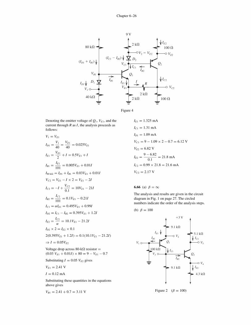
9 V
80 k� 100 �
100 �
2 k�
2 k�
2 k�
IB2
IR
40 k�
(ID1 � IB1)
ID1
(IC1 � IB2)
IE1
VE1
VE2
IE2
IC2
VC2
IC1
VB1
VC1
Q1
Q2
D1
D2
V1
V2 � VE2
IB1
Figure 4
Denoting the emitter voltage of Q1, VE1, and thecurrent through R as I , the analysis proceeds asfollows:
V1 = VE1
ID1 = V1
40= VE1
40= 0.025VE1
IE1 = VE1
2+ I = 0.5VE1 + I
IB1 = IE1
101= 0.005VE1 + 0.01I
I80 k� = ID1 + IB1 = 0.03VE1 + 0.01I
VC2 = VE1 − I × 2 = VE1 − 2I
IC2 = −I + VC2
0.1= 10VE1 − 21I
IB2 = IC2
101= 0.1VE1 − 0.21I
IC1 = αIE1 = 0.495VE1 + 0.99I
ID2 = IC1 − IB2 = 0.395VE1 + 1.2I
IE2 = IC2
α= 10.1VE1 − 21.2I
ID2 × 2 = IE2 × 0.1
2(0.395VE1 + 1.2I) = 0.1(10.1VE1 − 21.2I)
⇒ I = 0.05VE2
Voltage drop across 80-k� resistor =(0.03 VE1 + 0.01I) × 80 = 9 − VE1 − 0.7
Substituting I = 0.05 VE2 gives
VE1 = 2.41 V
I = 0.12 mA
Substituting these quantities in the equationsabove gives
VB1 = 2.41 + 0.7 = 3.11 V
IE1 = 1.325 mA
IC1 = 1.31 mA
ID1 = 1.09 mA
VC1 = 9 − 1.09 × 2 − 0.7 = 6.12 V
VE2 = 6.82 V
IE2 = 9 − 6.82
0.1= 21.8 mA
IC2 = 0.99 × 21.8 = 21.6 mA
VC2 = 2.17 V
6.66 (a) β = ∞The analysis and results are given in the circuitdiagram in Fig. 1 on page 27. The circlednumbers indicate the order of the analysis steps.
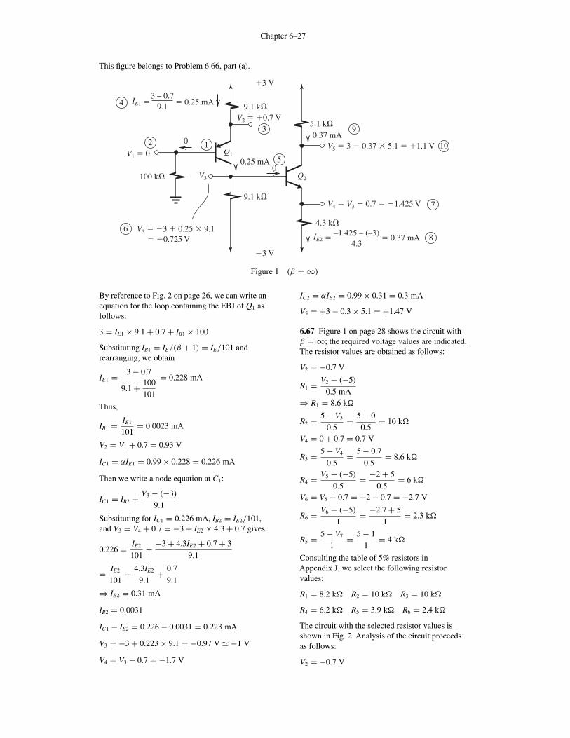
(b) β = 100
Figure 2 (β = 100)
Chapter 6–27
This figure belongs to Problem 6.66, part (a).
�3 V
�3 V
9.1 k�
5.1 k�
4.3 k�
3 – 0.79.1
9.1 k�
100 k�
0
IE1
Q1
Q2
V1 � 0
V3
V5 � 3 � 0.37 � 5.1 � �1.1 V
V4 � V3 � 0.7 � �1.425 V
V2 � �0.7 V
� 0.25 mA�
0.25 mA
0.37 mA
0
–1.425 – (–3)4.3
IE2 � 0.37 mA�
4
2
V3 � �3 � 0.25 � 9.1 � �0.725 V
6
3
5
9
10
8
7
1
Figure 1 (β = ∞)
By reference to Fig. 2 on page 26, we can write anequation for the loop containing the EBJ of Q1 asfollows:
3 = IE1 × 9.1 + 0.7 + IB1 × 100
Substituting IB1 = IE/(β + 1) = IE/101 andrearranging, we obtain
IE1 = 3 − 0.7
9.1 + 100
101
= 0.228 mA
Thus,
IB1 = IE1
101= 0.0023 mA
V2 = V1 + 0.7 = 0.93 V
IC1 = αIE1 = 0.99 × 0.228 = 0.226 mA
Then we write a node equation at C1:
IC1 = IB2 + V3 − (−3)
9.1
Substituting for IC1 = 0.226 mA, IB2 = IE2/101,and V3 = V4 + 0.7 = −3 + IE2 × 4.3 + 0.7 gives
0.226 = IE2
101+ −3 + 4.3IE2 + 0.7 + 3
9.1
= IE2
101+ 4.3IE2
9.1+ 0.7
9.1
⇒ IE2 = 0.31 mA
IB2 = 0.0031
IC1 − IB2 = 0.226 − 0.0031 = 0.223 mA
V3 = −3 + 0.223 × 9.1 = −0.97 V � −1 V
V4 = V3 − 0.7 = −1.7 V
IC2 = αIE2 = 0.99 × 0.31 = 0.3 mA
V5 = +3 − 0.3 × 5.1 = +1.47 V
6.67 Figure 1 on page 28 shows the circuit withβ = ∞; the required voltage values are indicated.The resistor values are obtained as follows:
V2 = −0.7 V
R1 = V2 − (−5)
0.5 mA⇒ R1 = 8.6 k�
R2 = 5 − V3
0.5= 5 − 0
0.5= 10 k�
V4 = 0 + 0.7 = 0.7 V
R3 = 5 − V4
0.5= 5 − 0.7
0.5= 8.6 k�
R4 = V5 − (−5)
0.5= −2 + 5
0.5= 6 k�
V6 = V5 − 0.7 = −2 − 0.7 = −2.7 V
R6 = V6 − (−5)
1= −2.7 + 5
1= 2.3 k�
R5 = 5 − V7
1= 5 − 1
1= 4 k�
Consulting the table of 5% resistors inAppendix J, we select the following resistorvalues:
R1 = 8.2 k� R2 = 10 k� R3 = 10 k�
R4 = 6.2 k� R5 = 3.9 k� R6 = 2.4 k�
The circuit with the selected resistor values isshown in Fig. 2. Analysis of the circuit proceedsas follows:
V2 = −0.7 V
Chapter 6–28
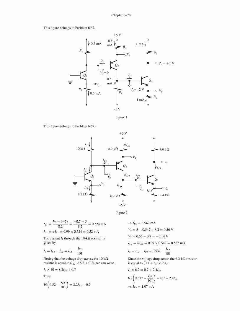
This figure belongs to Problem 6.67.
�5 V
–5 V
0.5 mA 1 mA
1 mA
0
0.5mA
0.5mA
R5
R6
V6
Q2
Q3
Q1
R2
R3
R1R4
V4
V2
0.5 mA
0V3 = 0
V5 = –2 V
V7 � �1 V
Figure 1
This figure belongs to Problem 6.67.
�5 V
–5 V
V6
Q2
Q3
Q1
V4
V7
V2
V3
I1
10 k� 8.2 k� 3.9 k�
8.2 k� 6.2 k� 2.4 k�
IC1
IB2
IB3
IE1I2
IE2
IE3
IC2
IC3
V5
Figure 2
IE1 = V2 − (−5)
8.2= −0.7 + 5
8.2= 0.524 mA
IC1 = αIE1 = 0.99 × 0.524 = 0.52 mA
The current I1 through the 10-k� resistor isgiven by
I1 = IC1 − IB2 = IC1 − IE2
101
Noting that the voltage drop across the 10 k�
resistor is equal to (IE2 × 8.2 + 0.7), we can write
I1 × 10 = 8.2IE2 + 0.7
Thus,
10
(0.52 − IE2
101
)= 8.2IE2 + 0.7
⇒ IE2 = 0.542 mA
V4 = 5 − 0.542 × 8.2 = 0.56 V
V3 = 0.56 − 0.7 = −0.14 V
IC2 = αIE2 = 0.99 × 0.542 = 0.537 mA
I2 = IC2 − IB3 = 0.537 − IE3
101
Since the voltage drop across the 6.2-k� resistoris equal to (0.7 + IE3 × 2.4),
I2 × 6.2 = 0.7 + 2.4IE3
6.2
(0.537 − IE3
101
)= 0.7 + 2.4IE3
⇒ IE3 = 1.07 mA
Chapter 6–29
V6 = −5 + 1.07 × 2.4 = −2.43 V
V5 = V6 + 0.7 = −1.73
IC3 = α × IE3 = 0.99 × 1.07 = 1.06 mA
V7 = −3.9 × 1.06 = 0.87 V
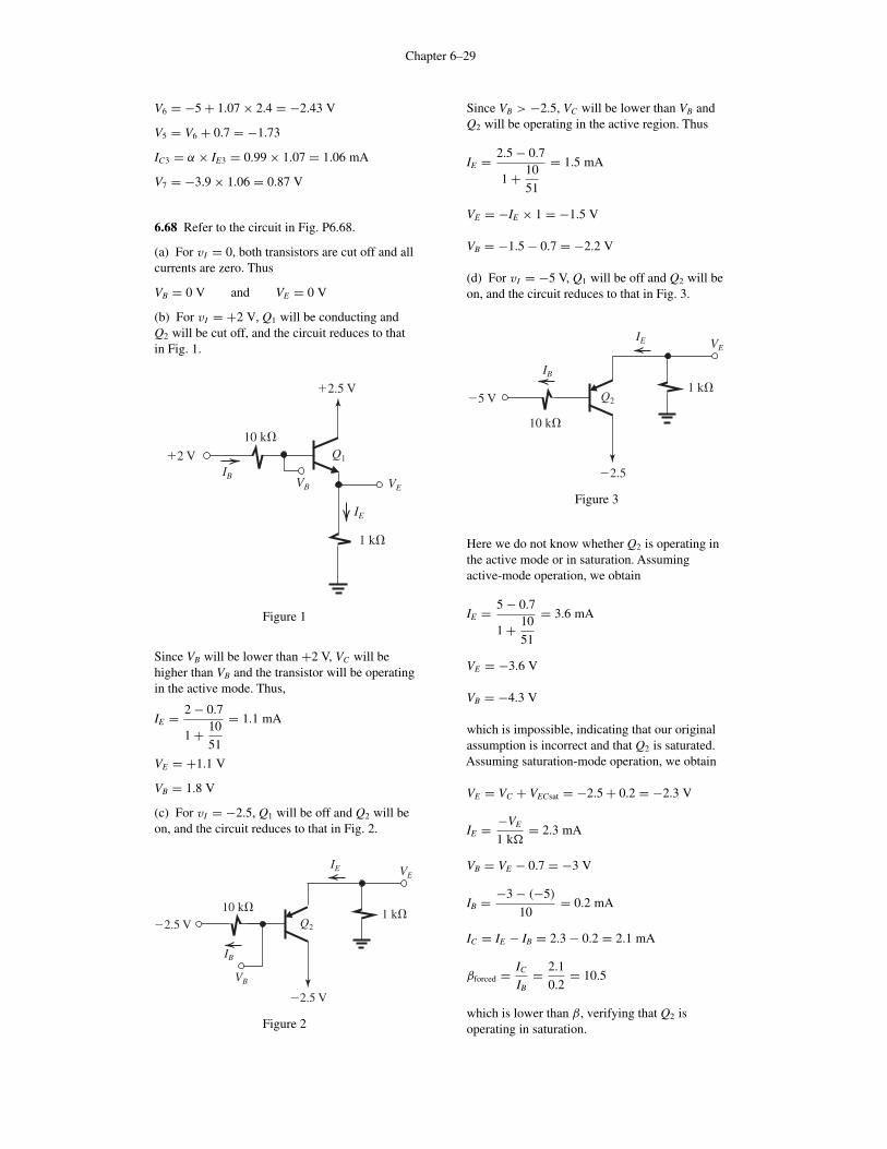
6.68 Refer to the circuit in Fig. P6.68.
(a) For v I = 0, both transistors are cut off and allcurrents are zero. Thus
VB = 0 V and VE = 0 V
(b) For v I = +2 V, Q1 will be conducting andQ2 will be cut off, and the circuit reduces to thatin Fig. 1.
10 k�
1 k�
�2 V
�2.5 V
IB
IE
VB
Q1
VE
Figure 1
Since VB will be lower than +2 V, VC will behigher than VB and the transistor will be operatingin the active mode. Thus,
IE = 2 − 0.7
1 + 10
51
= 1.1 mA
VE = +1.1 V
VB = 1.8 V
(c) For v I = −2.5, Q1 will be off and Q2 will beon, and the circuit reduces to that in Fig. 2.
Figure 2
Since VB > −2.5, VC will be lower than VB andQ2 will be operating in the active region. Thus
IE = 2.5 − 0.7
1 + 10
51
= 1.5 mA
VE = −IE × 1 = −1.5 V
VB = −1.5 − 0.7 = −2.2 V
(d) For v I = −5 V, Q1 will be off and Q2 will beon, and the circuit reduces to that in Fig. 3.
Figure 3
Here we do not know whether Q2 is operating inthe active mode or in saturation. Assumingactive-mode operation, we obtain
IE = 5 − 0.7
1 + 10
51
= 3.6 mA
VE = −3.6 V
VB = −4.3 V
which is impossible, indicating that our originalassumption is incorrect and that Q2 is saturated.Assuming saturation-mode operation, we obtain
VE = VC + VECsat = −2.5 + 0.2 = −2.3 V
IE = −VE
1 k�= 2.3 mA
VB = VE − 0.7 = −3 V
IB = −3 − (−5)
10= 0.2 mA
IC = IE − IB = 2.3 − 0.2 = 2.1 mA
βforced = IC
IB= 2.1
0.2= 10.5
which is lower than β, verifying that Q2 isoperating in saturation.
Chapter 6–30
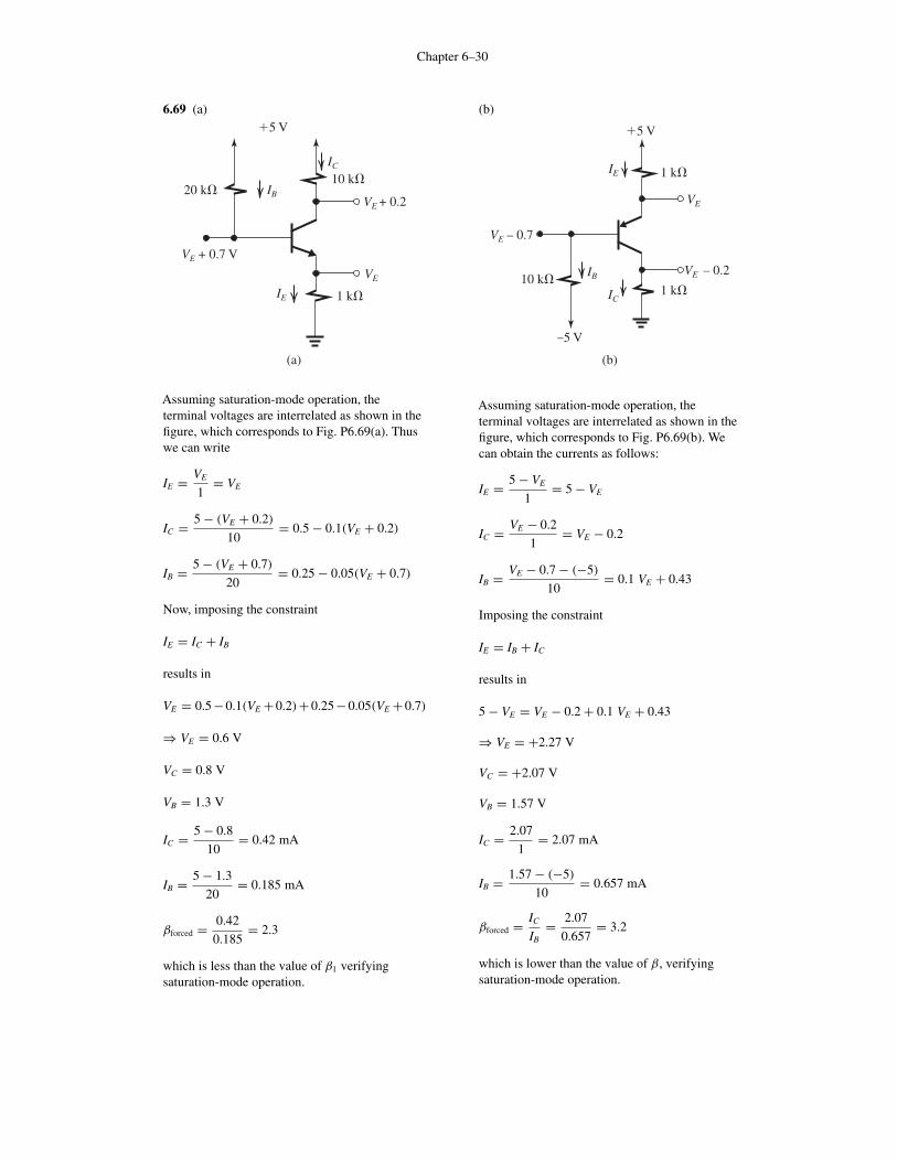
6.69 (a)
(a)
�5 V
20 k�10 k�
1 k�
VE + 0.7 V
IB
IC
IE
VE + 0.2
VE
Assuming saturation-mode operation, theterminal voltages are interrelated as shown in thefigure, which corresponds to Fig. P6.69(a). Thuswe can write
IE = VE
1= VE
IC = 5 − (VE + 0.2)
10= 0.5 − 0.1(VE + 0.2)
IB = 5 − (VE + 0.7)
20= 0.25 − 0.05(VE + 0.7)
Now, imposing the constraint
IE = IC + IB
results in
VE = 0.5−0.1(VE +0.2)+0.25−0.05(VE +0.7)
⇒ VE = 0.6 V
VC = 0.8 V
VB = 1.3 V
IC = 5 − 0.8
10= 0.42 mA
IB = 5 − 1.3
20= 0.185 mA
βforced = 0.42
0.185= 2.3
which is less than the value of β1 verifyingsaturation-mode operation.
(b)
(b)
�5 V
–5 V
1 k�
10 k�1 k�
VE – 0.7
IE
IB
IC
VE
VE – 0.2
Assuming saturation-mode operation, theterminal voltages are interrelated as shown in thefigure, which corresponds to Fig. P6.69(b). Wecan obtain the currents as follows:
IE = 5 − VE
1= 5 − VE
IC = VE − 0.2
1= VE − 0.2
IB = VE − 0.7 − (−5)
10= 0.1 VE + 0.43
Imposing the constraint
IE = IB + IC
results in
5 − VE = VE − 0.2 + 0.1 VE + 0.43
⇒ VE = +2.27 V
VC = +2.07 V
VB = 1.57 V
IC = 2.07
1= 2.07 mA
IB = 1.57 − (−5)
10= 0.657 mA
βforced = IC
IB= 2.07
0.657= 3.2
which is lower than the value of β, verifyingsaturation-mode operation.
Chapter 6–31
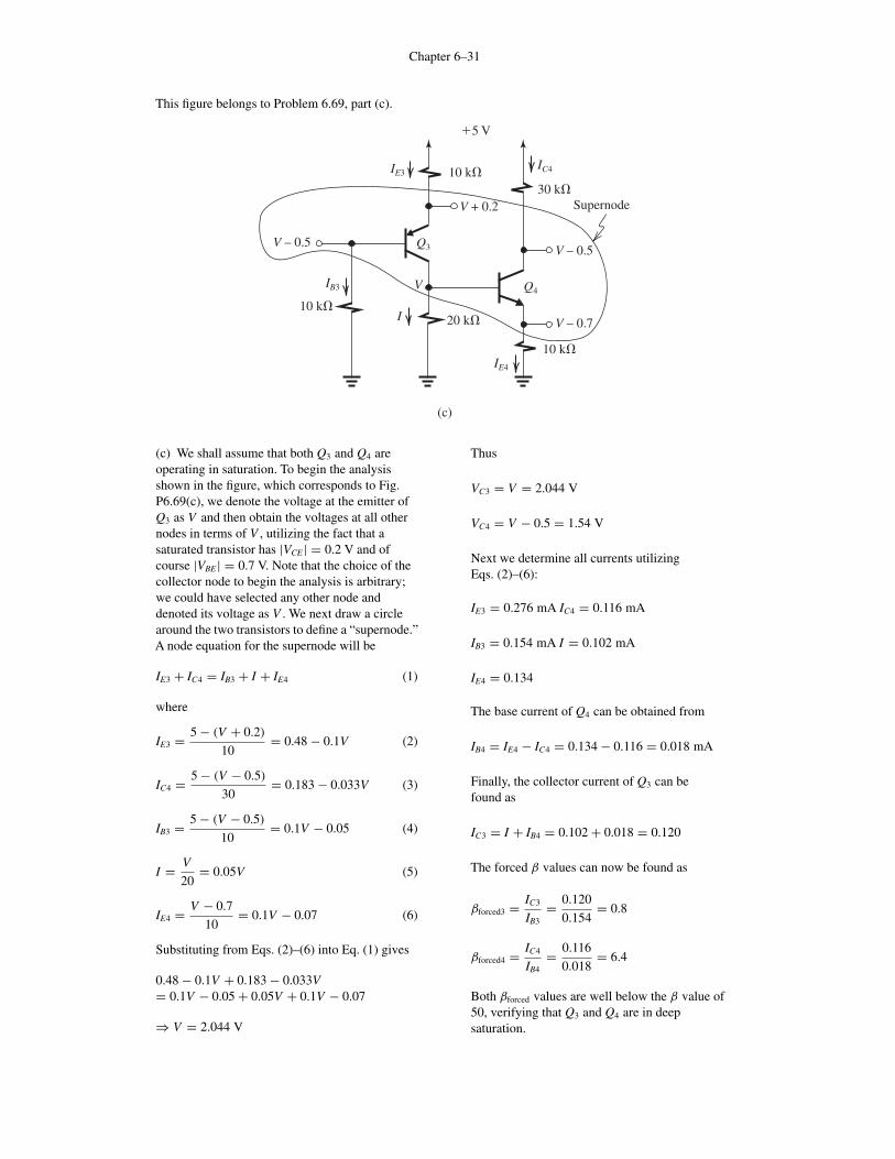
This figure belongs to Problem 6.69, part (c).
(c)
�5 V
Supernode
V
10 k�20 k�
10 k�
30 k�
10 k�
V – 0.5
IE3IC4
IE4
I
Q3
V + 0.2
V – 0.5
V – 0.7
IB3 Q4
(c) We shall assume that both Q3 and Q4 areoperating in saturation. To begin the analysisshown in the figure, which corresponds to Fig.P6.69(c), we denote the voltage at the emitter ofQ3 as V and then obtain the voltages at all othernodes in terms of V , utilizing the fact that asaturated transistor has |VCE | = 0.2 V and ofcourse |VBE | = 0.7 V. Note that the choice of thecollector node to begin the analysis is arbitrary;we could have selected any other node anddenoted its voltage as V . We next draw a circlearound the two transistors to define a “supernode.”A node equation for the supernode will be
IE3 + IC4 = IB3 + I + IE4 (1)
where
IE3 = 5 − (V + 0.2)
10= 0.48 − 0.1V (2)
IC4 = 5 − (V − 0.5)
30= 0.183 − 0.033V (3)
IB3 = 5 − (V − 0.5)
10= 0.1V − 0.05 (4)
I = V
20= 0.05V (5)
IE4 = V − 0.7
10= 0.1V − 0.07 (6)
Substituting from Eqs. (2)–(6) into Eq. (1) gives
0.48 − 0.1V + 0.183 − 0.033V= 0.1V − 0.05 + 0.05V + 0.1V − 0.07
⇒ V = 2.044 V
Thus
VC3 = V = 2.044 V
VC4 = V − 0.5 = 1.54 V
Next we determine all currents utilizingEqs. (2)–(6):
IE3 = 0.276 mA IC4 = 0.116 mA
IB3 = 0.154 mA I = 0.102 mA
IE4 = 0.134
The base current of Q4 can be obtained from
IB4 = IE4 − IC4 = 0.134 − 0.116 = 0.018 mA
Finally, the collector current of Q3 can befound as
IC3 = I + IB4 = 0.102 + 0.018 = 0.120
The forced β values can now be found as
βforced3 = IC3
IB3= 0.120
0.154= 0.8
βforced4 = IC4
IB4= 0.116
0.018= 6.4
Both βforced values are well below the β value of50, verifying that Q3 and Q4 are in deepsaturation.


![Data Structures - cs.bgu.ac.ilds152/wiki.files/Presentation17[1].pdf · Shortest Path •Let u, v ∈ V •The shortest-path weight u to v is •The shortest path u to v is any path](https://static.fdocument.org/doc/165x107/5f59ef12a2afa65ee75af138/data-structures-csbguacil-ds152wikifilespresentation171pdf-shortest.jpg)