EE 435 Lecture 14 Two-Stage Op Amp Design
47
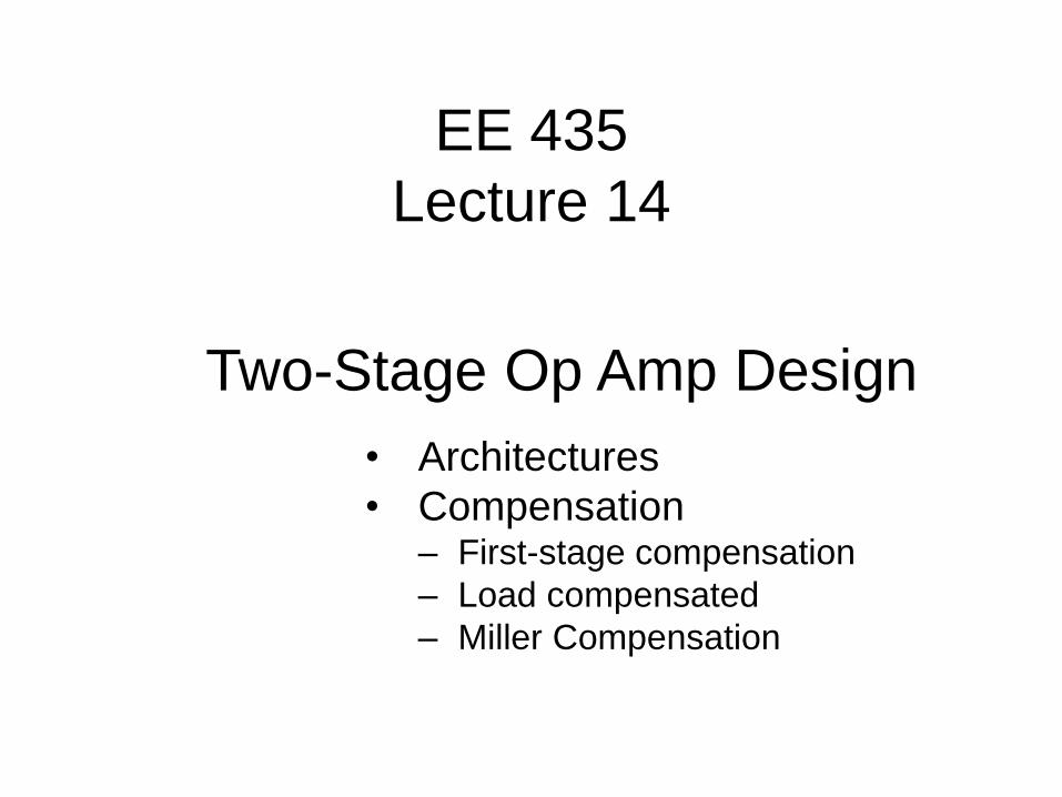
EE 435 Lecture 14 Two-Stage Op Amp Design • Architectures • Compensation ‒ First-stage compensation ‒ Load compensated ‒ Miller Compensation
Transcript of EE 435 Lecture 14 Two-Stage Op Amp Design
EE 435
Lecture 14
Two-Stage Op Amp Design
• Architectures
• Compensation‒ First-stage compensation
‒ Load compensated
‒ Miller Compensation

Cascaded Amplifier Summary
Four or more amplifier cascades - problems even larger than for three stages
-- seldom used in industry !
-- seldom used in industry !
Two amplifier cascades – for separated poles 0TOT0TOT A2βkA4β
-- widely used in industry but compensation is essential
-- spread dependent upon β and most stringent for large β
Three amplifier cascades - for ideally identical stages 3
0βA8
Single-stage amplifiers
-- widely used in industry, little or no concern about compensation
Note: Some amplifiers that are termed single-stage amplifiers in many books and papers are
actually two-stage amplifiers and some require modest compensation. Some that are termed two-
stage amplifiers are actually three-stage amplifiers. These invariable have a very small gain on the
first stage and a very large bandwidth. The nomenclature on this summary refers to the number of
stages that have reasonably large gain.
0 A pA
s p
Three amplifier cascades - for separated poles
-- seldom used in industry but starting to appear but compensation essential!
0TOT323232 βAkkkkkk1
2 1p =kpReview from Last Time
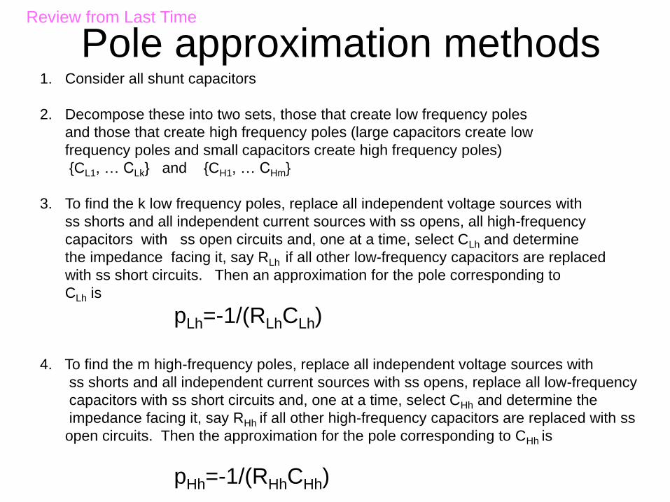
Pole approximation methods1. Consider all shunt capacitors
2. Decompose these into two sets, those that create low frequency poles
and those that create high frequency poles (large capacitors create low
frequency poles and small capacitors create high frequency poles)
{CL1, … CLk} and {CH1, … CHm}
3. To find the k low frequency poles, replace all independent voltage sources with
ss shorts and all independent current sources with ss opens, all high-frequency
capacitors with ss open circuits and, one at a time, select CLh and determine
the impedance facing it, say RLh if all other low-frequency capacitors are replaced
with ss short circuits. Then an approximation for the pole corresponding to
CLh is
pLh=-1/(RLhCLh)
4. To find the m high-frequency poles, replace all independent voltage sources with
ss shorts and all independent current sources with ss opens, replace all low-frequency
capacitors with ss short circuits and, one at a time, select CHh and determine the
impedance facing it, say RHh if all other high-frequency capacitors are replaced with ss
open circuits. Then the approximation for the pole corresponding to CHh is
pHh=-1/(RHhCHh)
Review from Last Time
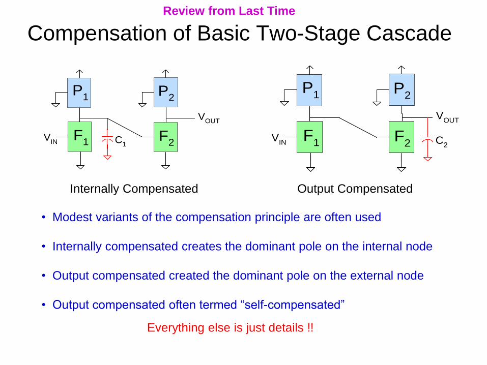
Compensation of Basic Two-Stage Cascade
F1
P1
VIN
F2
P2
VOUT
C1
• Modest variants of the compensation principle are often used
• Internally compensated creates the dominant pole on the internal node
• Output compensated created the dominant pole on the external node
• Output compensated often termed “self-compensated”
F1
P1
VIN
F2
P2
VOUT
C2
Internally Compensated Output Compensated
Everything else is just details !!
Review from Last Time

Im
45o
Maximally fast time-domain
response w/o ringing
Maximally Flat
Magnitude Response
Re
Typical Preferred
Pole Locations
Q=.707
Q=.5
Typical Target Closed-loop Pole Locations for Feedback Amplifiers
Review from Last Time
Common Compensation Goal
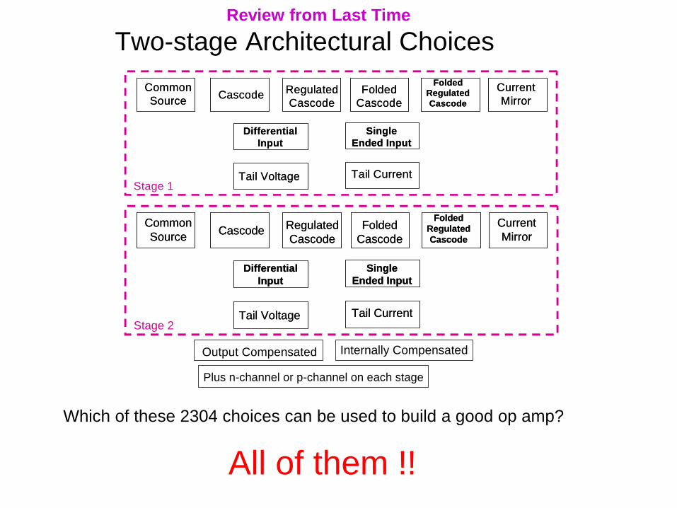
Two-stage Architectural Choices
Which of these 2304 choices can be used to build a good op amp?
All of them !!
Output Compensated Internally Compensated
Plus n-channel or p-channel on each stage
Common
SourceCascode
Regulated
Cascode
Folded
Cascode
Folded
Regulated
Cascode
Current
Mirror
Common
SourceCascode
Regulated
Cascode
Folded
Cascode
Folded
Regulated
Cascode
Current
Mirror
Differential
Input
Differential
Input
Single
Ended Input
Single
Ended Input
Tail Voltage Tail CurrentTail Voltage Tail CurrentStage 1
Common
SourceCascode
Regulated
Cascode
Folded
Cascode
Folded
Regulated
Cascode
Current
Mirror
Common
SourceCascode
Regulated
Cascode
Folded
Cascode
Folded
Regulated
Cascode
Current
Mirror
Differential
Input
Differential
Input
Single
Ended Input
Single
Ended Input
Tail Voltage Tail CurrentTail Voltage Tail CurrentStage 2
Review from Last Time

Two-stage Architectural Choices
Guidelines for Architectural Choices
Tail current source usually used in first stage, tail voltage source in second
stage
Large gain usually used in first stage, smaller gain in second stage
First and second stage usually use quarter circuits of opposite types (n-p
or p-n)
Input common mode input range of concern on first stage but output swing
of first stage of reduced concern. Output range on second stage of
concern.
CMRR of first stage of concern but not of second stage
Noise on first stage of concern but not of much concern on second stage
Offset voltage usually dominated by that of the first stage
Review from Last Time
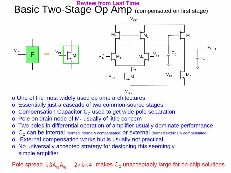
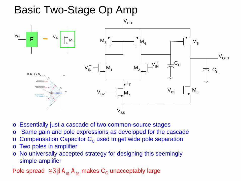
Basic Two-Stage Op Amp (compensated on first stage)
VDD
VSS
M1
M2
M3 M
4M
5
CL
VIN
VOUT
M6M
7
IT
VB2
VB3
VIN
CC
o One of the most widely used op amp architectures
o Essentially just a cascade of two common-source stages
o Compensation Capacitor CC used to get wide pole separation
o Pole on drain node of M1 usually of little concern
o Two poles in differential operation of amplifier usually dominate performance
o CC can be internal (termed internally compensated) or external (termed externally compensated)
o External compensation works but is usually not practical
o No universally accepted strategy for designing this seemingly
simple amplifier
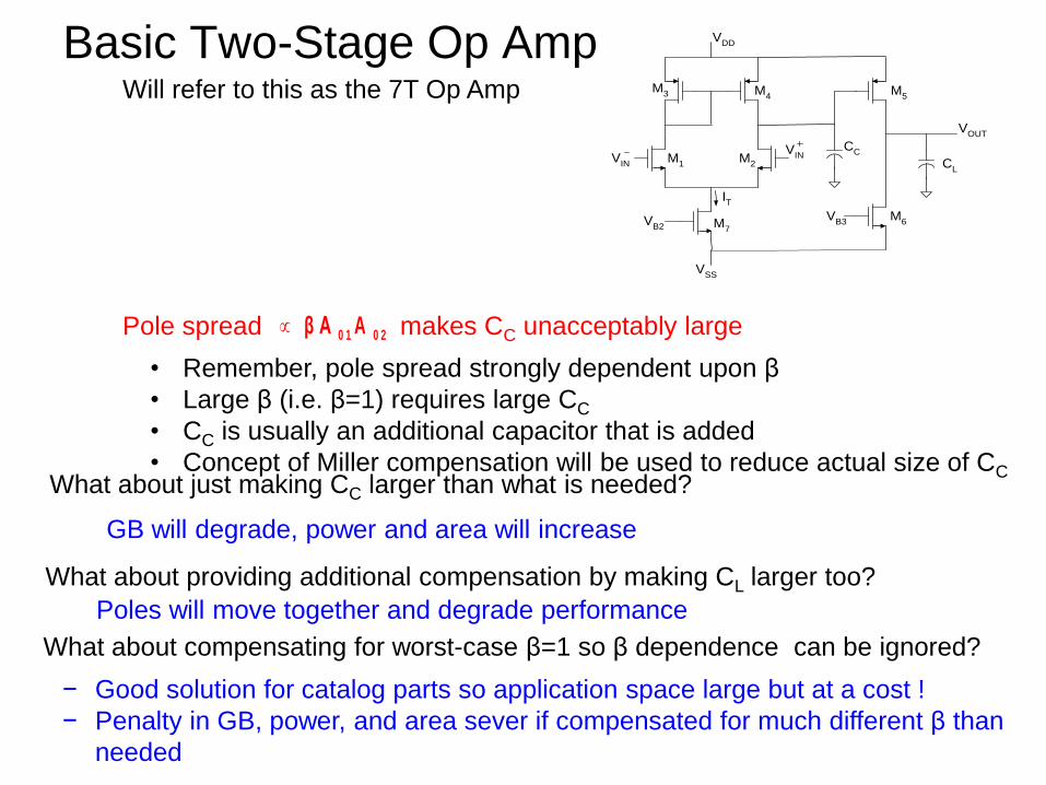
Pole spread makes CC unacceptably large for on-chip solutions01 02k β A A 2 k 4
Review from Last Time
FVIN VIN
M1
Basic Two-Stage Op Amp VDD
VSS
M1
M2
M3 M
4M
5
CL
VIN
VOUT
M6M
7
IT
VB2
VB3
VIN
CC
Pole spread makes CC unacceptably large0 20 1 Aβ A
What about just making CC larger than what is needed?
• Remember, pole spread strongly dependent upon β
• Large β (i.e. β=1) requires large CC
• CC is usually an additional capacitor that is added
• Concept of Miller compensation will be used to reduce actual size of CC
What about providing additional compensation by making CL larger too?
What about compensating for worst-case β=1 so β dependence can be ignored?
GB will degrade, power and area will increase
Poles will move together and degrade performance
− Good solution for catalog parts so application space large but at a cost !
− Penalty in GB, power, and area sever if compensated for much different β than
needed
Will refer to this as the 7T Op Amp
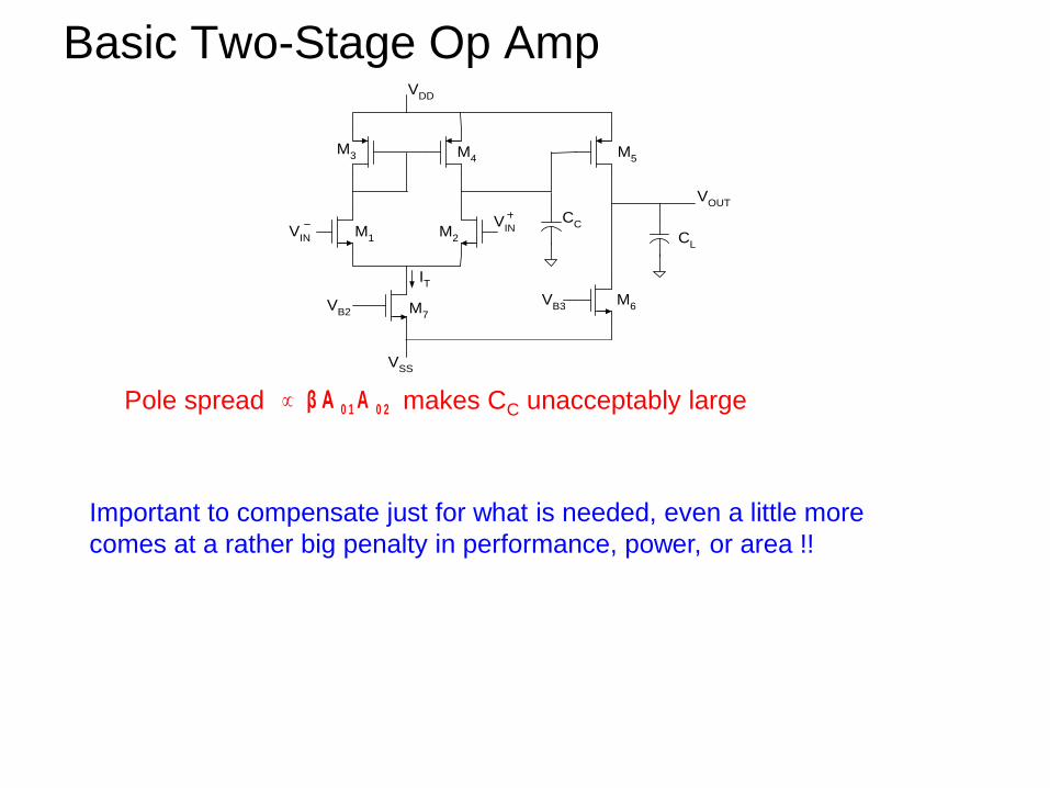
Basic Two-Stage Op AmpV
DD
VSS
M1
M2
M3 M
4M
5
CL
VIN
VOUT
M6M
7
IT
VB2
VB3
VIN
CC
Pole spread makes CC unacceptably large0 20 1 Aβ A
Important to compensate just for what is needed, even a little more
comes at a rather big penalty in performance, power, or area !!

Selected Commercial Op Amps
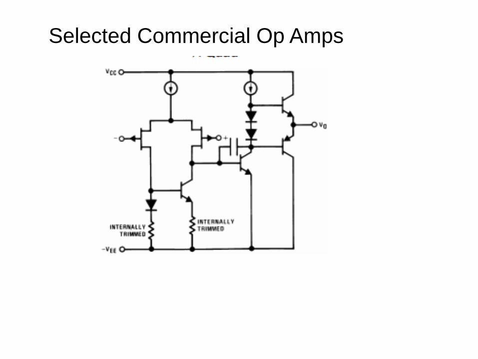
Selected Commercial Op Amps
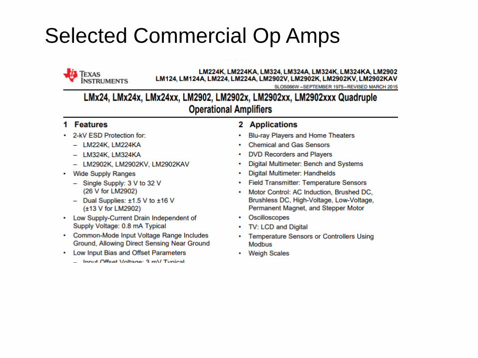
Selected Commercial Op Amps

Selected Commercial Op Amps
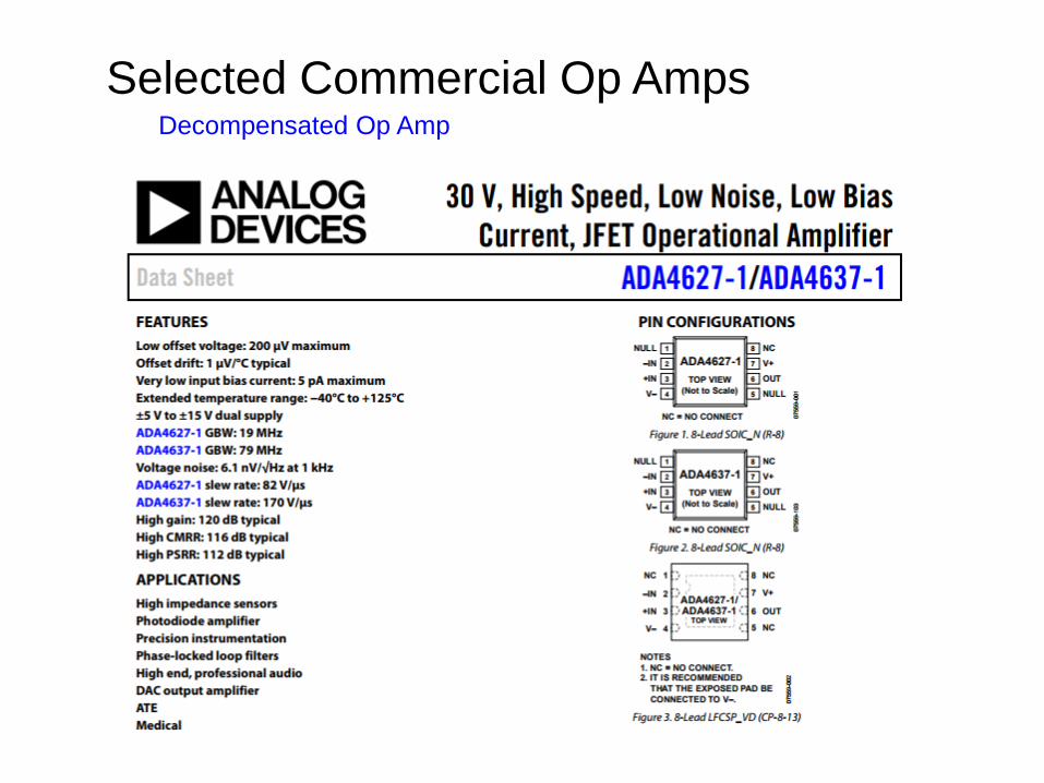
Decompensated Op Amp
Selected Commercial Op Amps
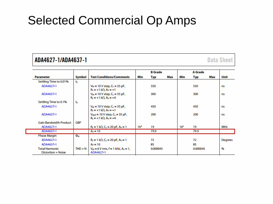
Selected Commercial Op Amps
Example:Sketch the circuit of a two-stage internally compensated op amp with a
telescopic cascode first stage, single-ended output, tail current bias first
stage, tail voltage bias second stage, p-channel inputs and n-channel
inputs on the second stage.
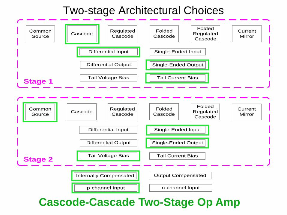
Two-stage Architectural Choices
Common
SourceCascode
Regulated
Cascode
Folded
Cascode
Folded
Regulated
Cascode
Current
Mirror
Differential Input Single-Ended Input
Differential Output Single-Ended Output
Tail Voltage Bias Tail Current BiasStage 1
Internally Compensated Output Compensated
Common
SourceCascode
Regulated
Cascode
Folded
Cascode
Folded
Regulated
Cascode
Current
Mirror
Differential Input Single-Ended Input
Differential Output Single-Ended Output
Tail Voltage Bias Tail Current BiasStage 2
p-channel Input n-channel Input
Cascode-Cascade Two-Stage Op Amp

Example Solution
CC
VOUT
VINVIN
VDD
VX3
VX4 VX5
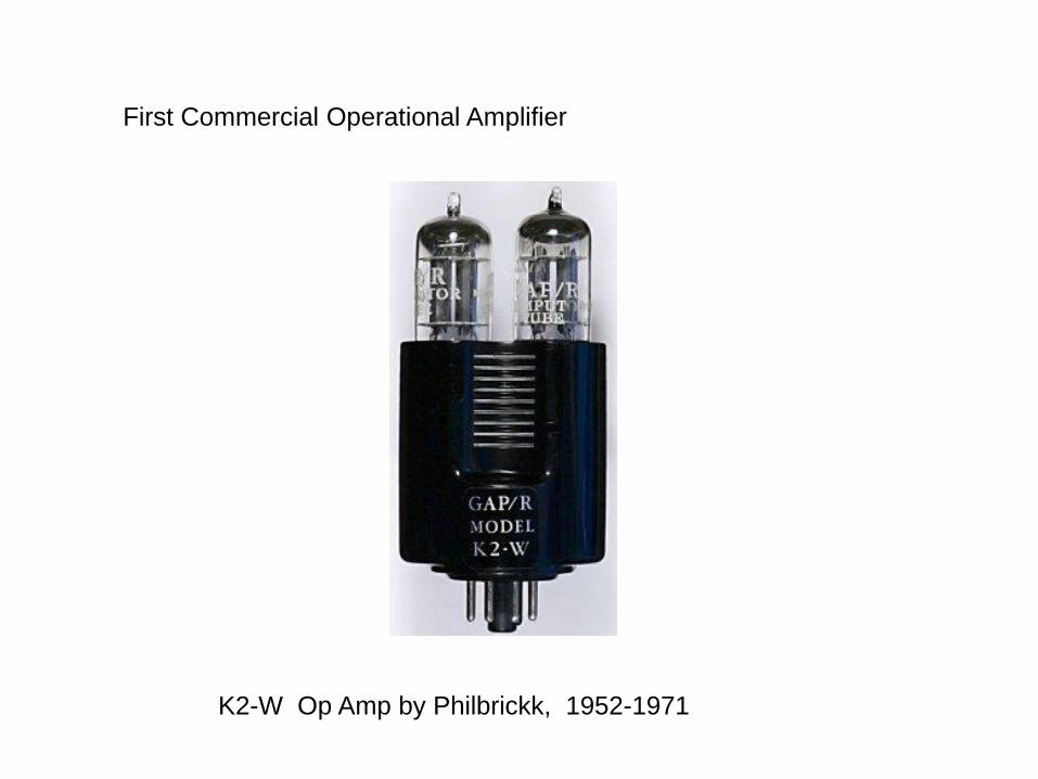
K2-W Op Amp by Philbrickk, 1952-1971
First Commercial Operational Amplifier

“Widlar began his career at Fairchild semiconductor, where he designed a
couple of pioneering op amps. By 1966, the commercial success of his
designs became apparent, and Widlar asked for a raise. He was turned down,
and jumped ship to the fledgling National Semiconductor. At National he
continued to turn out amazing designs, and was able to retire just before his
30th birthday in 1970.”
Inventor of the Two-Stage Op Amp
Robert Widlar
Many say he started the field of analog IC design, considered a brilliant engineer
(from posted www site)
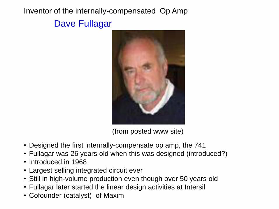
Inventor of the internally-compensated Op Amp
Dave Fullagar
• Designed the first internally-compensate op amp, the 741
• Fullagar was 26 years old when this was designed (introduced?)
• Introduced in 1968
• Largest selling integrated circuit ever
• Still in high-volume production even though over 50 years old
• Fullagar later started the linear design activities at Intersil
• Cofounder (catalyst) of Maxim
(from posted www site)

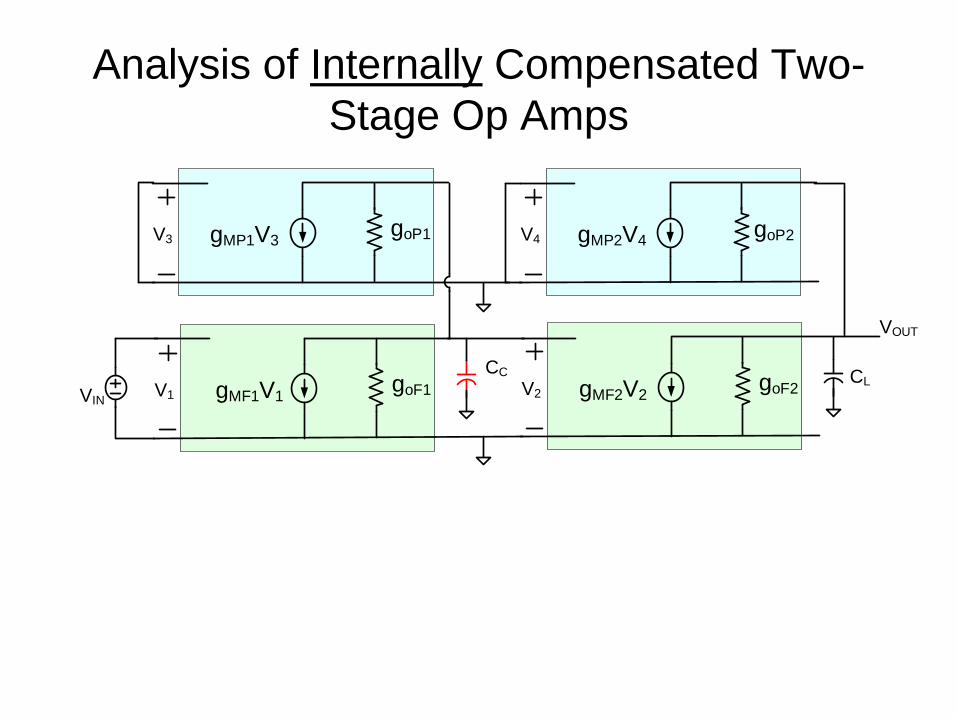
Analysis of Internally Compensated Two-
Stage Op Amps
F1
P1
VIN
F2
P2
VOUT
CC
CL
Can’t get everything but can get most of the small-signal results
Consider single-ended input-output (differential analysis only slightly different)
Since internally compensated, must have p1<<p2
p1 pole on first stage, p2 pole on second stage
Analysis of Internally Compensated Two-
Stage Op Amps
|p1| |p2|
ω
A0
0
1 2
AA s =
s s+1 +1
p p
For |p1| << |p2|
BW ≈ |p1|
Analysis of Internally Compensated Two-
Stage Op Amps
goF1gMF1V1V1
CCgoF2gMF2V2V2
CL
goP2gMP2V4V4goP1gMP1V3V3
VIN
VOUT
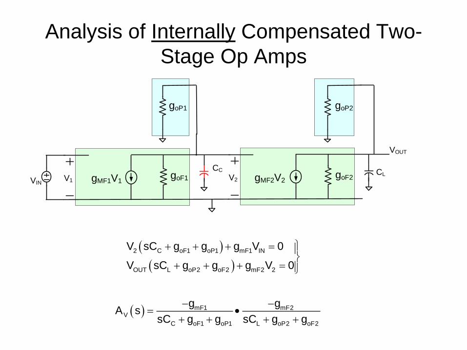
Analysis of Internally Compensated Two-
Stage Op Amps
goF1gMF1V1V1
CCgoF2gMF2V2V2
CL
goP2goP1
VIN
VOUT
2 C oF1 oP1 mF1 IN
OUT L oP2 oF2 mF2 2
V sC g g g V 0
V sC g g g V 0
mF1 mF2V
C oF1 oP1 L oP2 oF2
g gA s
sC g g sC g g

Analysis of Internally Compensated Two-
Stage Op Amps
goF1gMF1V1V1
CCgoF2gMF2V2V2
CL
goP2goP1
VIN
VOUT
C
oP1oF11
C
ggp
L
oP2oF22
C
ggp
oP2oF2
mF2
oP1oF1
mF1V0
gg
g
gg
gA
1pBW
CoP2oF2
mF2mF1
Cgg
ggGB
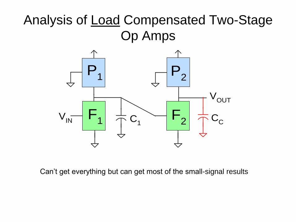
Analysis of Load Compensated Two-Stage
Op Amps
F1
P1
VIN
F2
P2
VOUT
C1
CC
Can’t get everything but can get most of the small-signal results
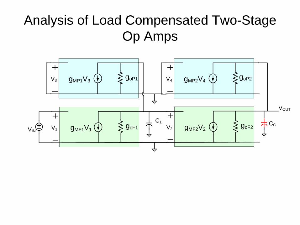
Analysis of Load Compensated Two-Stage
Op Amps
goF1gMF1V1V1
C1goF2gMF2V2V2
CC
goP2gMP2V4V4goP1gMP1V3V3
VIN
VOUT
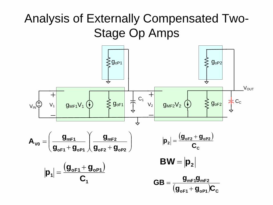
Analysis of Externally Compensated Two-
Stage Op Amps
1
oP1oF11
C
ggp
C
oP2oF22
C
ggp
oP2oF2
mF2
oP1oF1
mF1V0
gg
g
gg
gA
2pBW
CoP1oF1
mF2mF1
Cgg
ggGB
goF1gMF1V1V1
C1goF2gMF2V2V2
CC
goP2goP1
VIN
VOUT
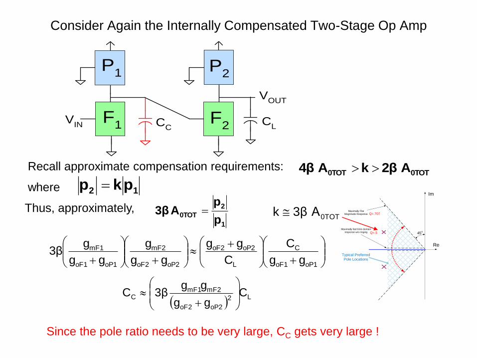
Consider Again the Internally Compensated Two-Stage Op Amp
F1
P1
VIN
F2
P2
VOUT
CC
CL
0TOT0TOT A2βkA4β
Since the pole ratio needs to be very large, CC gets very large !
12 pkp
1
2
0TOTp
pA3β
oP1oF1
C
L
oP2oF2
oP2oF2
mF2
oP1oF1
mF1
gg
C
C
gg
gg
g
gg
g3β
L2
oP2oF2
mF2mF1C C
gg
gg3βC
Recall approximate compensation requirements:
where
Thus, approximately,
Im
45o
Maximally fast time-domain
response w/o ringing
Maximally Flat
Magnitude Response
Re
Typical Preferred
Pole Locations
Q=.707
Q=.5
0TOTk 3β A
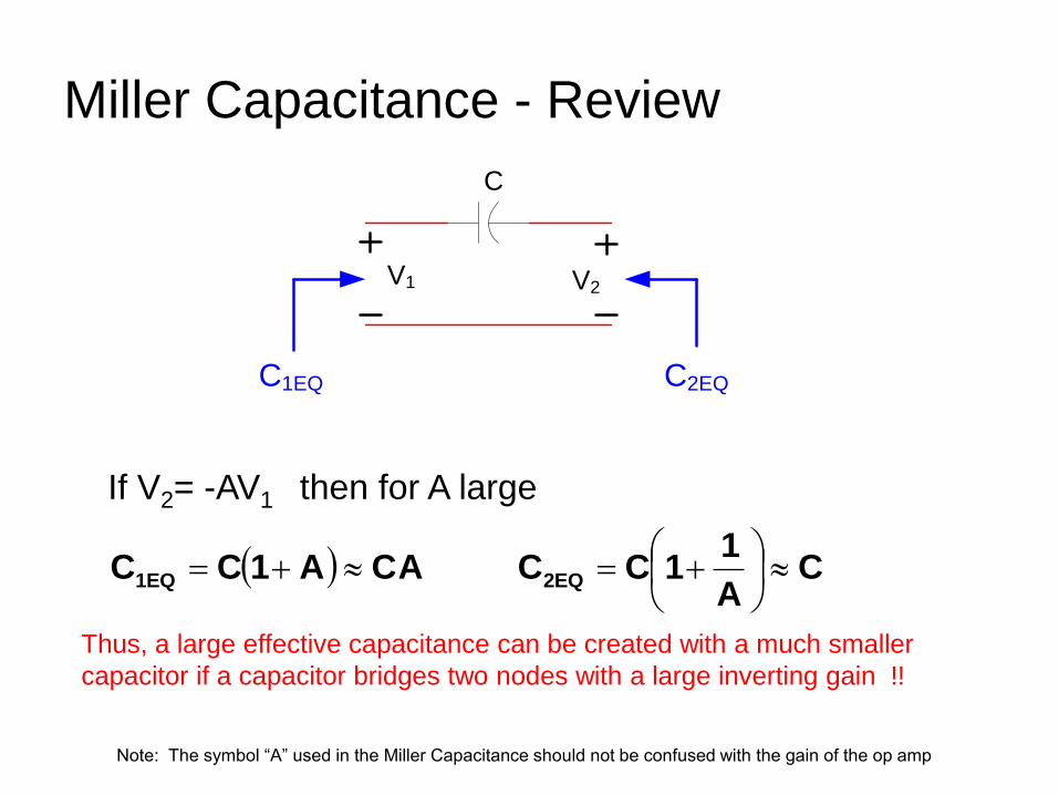
Miller Capacitance - Review
If V2= -AV1 then for A large
CA
11CCCAA1CC 2EQ1EQ
Thus, a large effective capacitance can be created with a much smaller
capacitor if a capacitor bridges two nodes with a large inverting gain !!
V1 V2
C
C1EQ C2EQ
Note: The symbol “A” used in the Miller Capacitance should not be confused with the gain of the op amp
Miller Capacitance - Review
If V2= -AV1 then for A large
CA
11CCCAA1CC 2EQ1EQ
• If A changes with frequency, C1EQ and C2EQ are no longer pure capacitors
• More useful for giving a concept than for accurate actual analysis because of
frequency dependence of A
V1 V2C1EQ C2EQV1 V2
C
C1EQ C2EQ
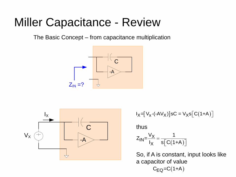
Miller Capacitance - Review
ZIN =?
C
-A
The Basic Concept – from capacitance multiplication
C
-A
IX
VX
X x X XI = V -(-AV ) sC = V s C 1+A
thus
X
INX
V 1Z =
I s C 1+A
So, if A is constant, input looks like
a capacitor of value
EQC =C 1+A
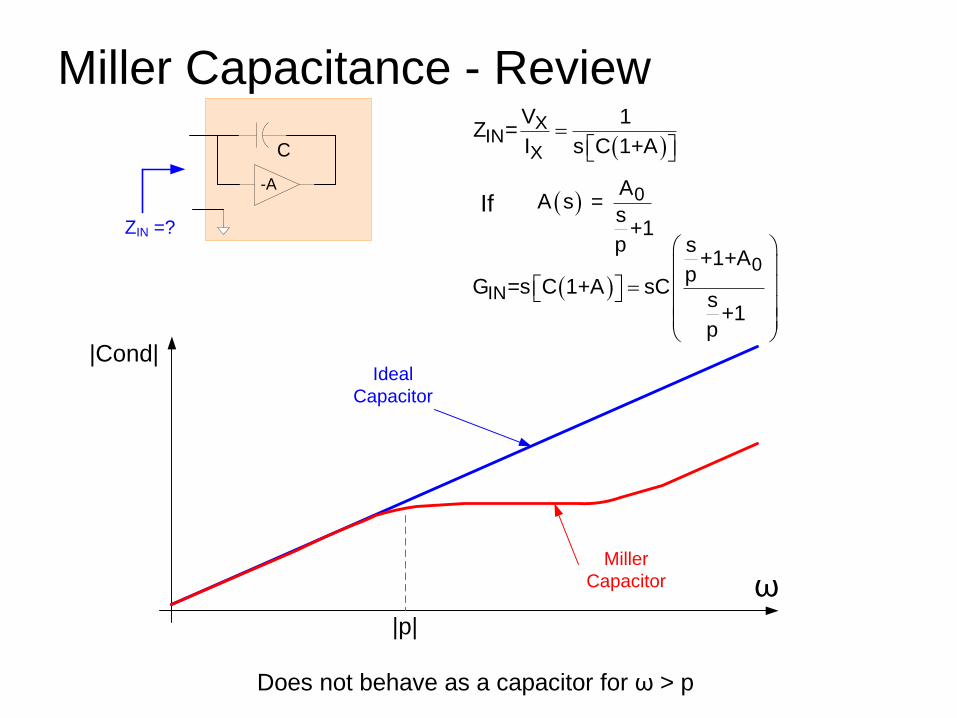
Miller Capacitance - Review
ω
|p|
|Cond|Ideal
Capacitor
Miller
Capacitor
X
INX
V 1Z =
I s C 1+A
ZIN =?
C
-A
If 0AA s =
s+1
p
0
IN
s+1+A
pG =s C 1+A sC
s+1
p
Does not behave as a capacitor for ω > p
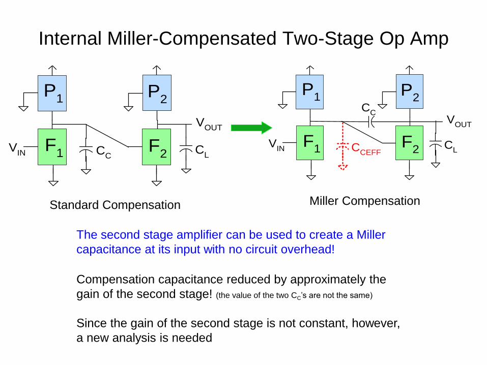
Internal Miller-Compensated Two-Stage Op Amp
F1
P1
VIN
F2
P2
VOUT
CC
CL
Standard Compensation Miller Compensation
F1
P1
VIN
F2
P2
VOUT
CC
CLC
CEFF
Compensation capacitance reduced by approximately the
gain of the second stage! (the value of the two CC’s are not the same)
Since the gain of the second stage is not constant, however,
a new analysis is needed
The second stage amplifier can be used to create a Miller
capacitance at its input with no circuit overhead!
F1
P1
VIN
F2
P2
VOUT
CC
CLC
CEFF
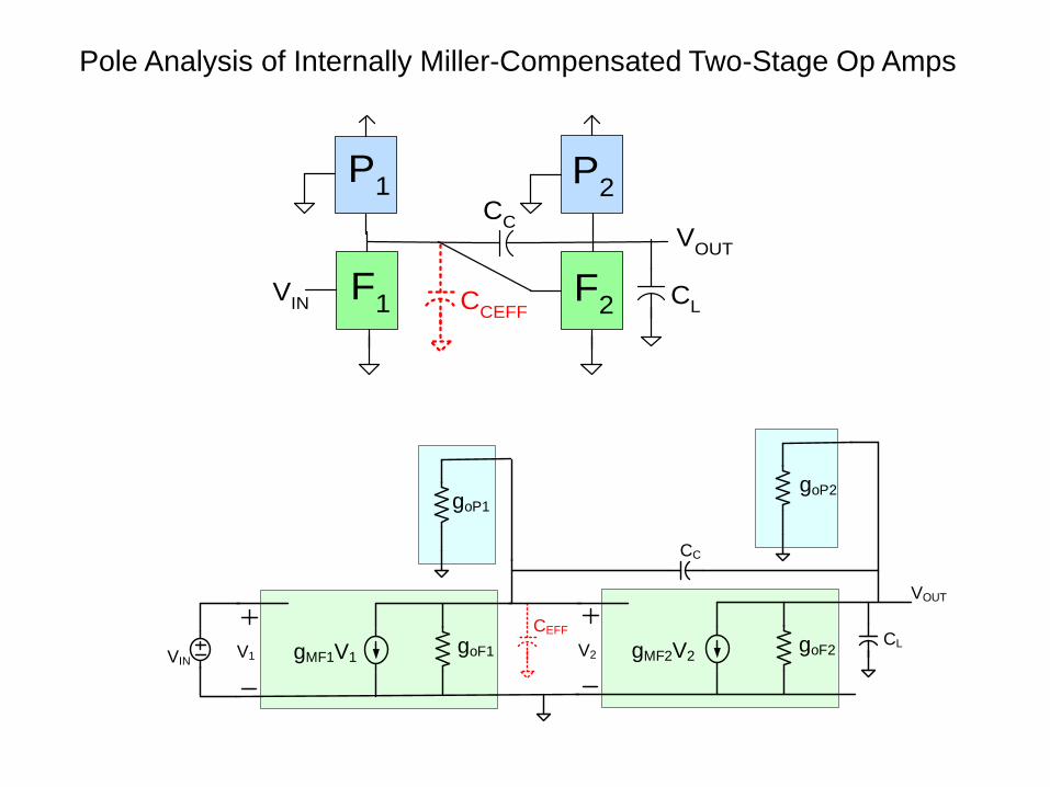
Pole Analysis of Internally Miller-Compensated Two-Stage Op Amps
goF1gMF1V1V1
CEFF
goF2gMF2V2V2
CL
goP2goP1
VIN
VOUT
CC
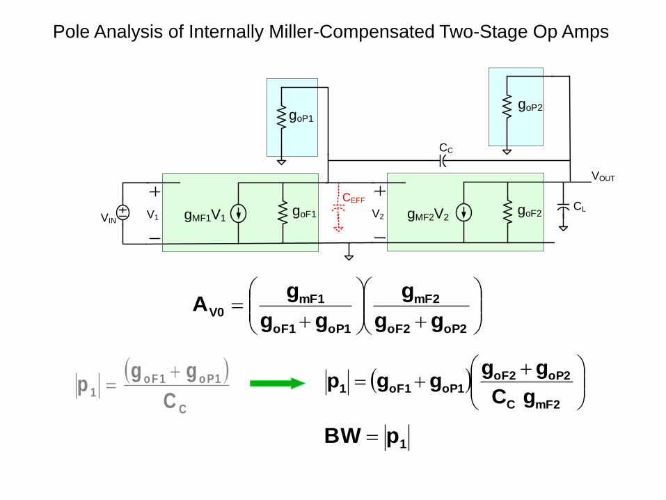
Pole Analysis of Internally Miller-Compensated Two-Stage Op Amps
C
o P1o F 11
C
ggp
mF2C
oP2oF2oP1oF11
gC
ggggp
1pBW
oP2oF2
mF2
oP1oF1
mF1V0
gg
g
gg
gA
goF1gMF1V1V1
CEFF
goF2gMF2V2V2
CL
goP2goP1
VIN
VOUT
CC
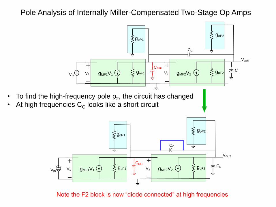
Pole Analysis of Internally Miller-Compensated Two-Stage Op Amps
• To find the high-frequency pole p2, the circuit has changed
• At high frequencies CC looks like a short circuit
Note the F2 block is now “diode connected” at high frequencies
goF1gMF1V1V1
CEFF
goF2gMF2V2V2
CL
goP2goP1
VIN
VOUT
CC
goF1gMF1V1V1
CEFF
goF2gMF2V2V2
CL
goP2goP1
VIN
VOUT
CC
Pole Analysis of Internally Miller-Compensated Two-Stage Op Amps
L
o P2o F 22
C
ggp
L
mF22
C
gp
oP2oF2
mF2
oP1oF1
mF1V0
gg
g
gg
gA
C
mF1
C
gGB Co P2o F 2
mF 2mF 1
Cgg
ggGB
goF1gMF1V1V1gMF2
CL
goP2goP1
VIN
VOUT
CC
goF2
oF2 oP2 oF1 oP1oF1 oP1
C mF2 EFF
g g g gBW g g
C g C
1 2
2
2 0 1 0 1 0 2 0 2
1
1
mF mF
C L C mF F P F P
g g
A ss g
s
z
C C sC g g g g
If zero does not affect GB
Will be shown later that CC introduces a zero in the gain function

Pole Analysis of Internally Miller-Compensated Two-Stage Op Amps
L
o P2o F 22
C
ggp
L
mF22
C
gp
oP2oF2
mF2
oP1oF1
mF1V0
gg
g
gg
gA
C
mF1
C
gGB
Co P2o F 2
mF 2mF 1
Cgg
ggGB
Has the GB decreased?
No, because the CC decreased by the same factor!
goF1gMF1V1V1gMF2
CL
goP2goP1
VIN
VOUT
CC
oF2 oP2 oF1 oP1oF1 oP1
C mF2 EFF
g g g gBW g g
C g C
If zero does not affect GB
Basic Two-Stage Op AmpV
DD
VSS
M1
M2
M3 M
4M
5
CL
VIN
VOUT
M6M
7
IT
VB2
VB3
VIN
CC
o Essentially just a cascade of two common-source stages
o Same gain and pole expressions as developed for the cascade
o Compensation Capacitor CC used to get wide pole separation
o Two poles in amplifier
o No universally accepted strategy for designing this seemingly
simple amplifier
Pole spread makes CC unacceptably large 01 023 β A A
FVIN VIN
M1
Im
45o
Maximally fast time-domain
response w/o ringing
Maximally Flat
Magnitude Response
Re
Typical Preferred
Pole Locations
Q=.707
Q=.5
0TOTk 3β A
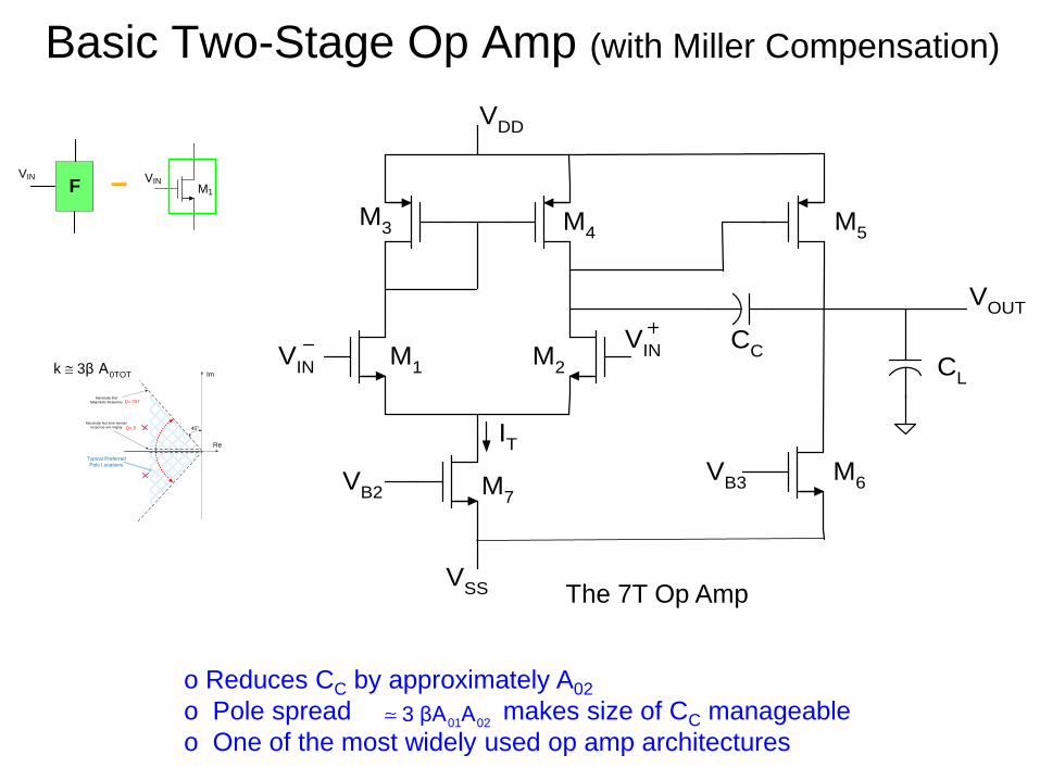
Basic Two-Stage Op Amp (with Miller Compensation)
o Reduces CC by approximately A02
o Pole spread makes size of CC manageable
o One of the most widely used op amp architectures01 023 βA A
VDD
VSS
M1
M2
M3 M
4M
5
CL
VIN
VOUT
M6M
7
IT
VB2
VB3
VIN
CC
The 7T Op Amp
FVIN VIN
M1
Im
45o
Maximally fast time-domain
response w/o ringing
Maximally Flat
Magnitude Response
Re
Typical Preferred
Pole Locations
Q=.707
Q=.5
0TOTk 3β A
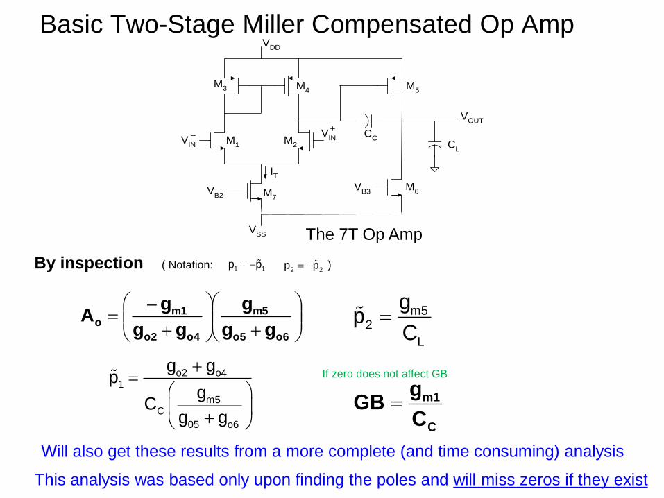
Basic Two-Stage Miller Compensated Op Amp
o6o5
m5
o4o2
m1o
gg
g
gg
gA
o2 o41
m5C
05 o6
g gp
gC
g g
m52
L
gp
C
C
m1
C
gGB
By inspection ( Notation: )
VDD
VSS
M1
M2
M3 M
4M
5
CL
VIN
VOUT
M6M
7
IT
VB2
VB3
VIN
CC
Will also get these results from a more complete (and time consuming) analysis
This analysis was based only upon finding the poles and will miss zeros if they exist
If zero does not affect GB
1 1p p 2 2p p
The 7T Op Amp

Stay Safe and Stay Healthy !

End of Lecture 14