Site directed mutagenesis of β2-microglobulin PowerPoint Presentation
San Jose State University San Jose State University
SJSU ScholarWorks SJSU ScholarWorks
Master's Theses Master's Theses and Graduate Research
Fall 2016
Directed Self-Assembly of High-χ Block Copolymers for Advanced Directed Self-Assembly of High- Block Copolymers for Advanced
Patterning Applications Patterning Applications
Gabriela Alva San Jose State University
Follow this and additional works at: https://scholarworks.sjsu.edu/etd_theses
Recommended Citation Recommended Citation Alva, Gabriela, "Directed Self-Assembly of High-χ Block Copolymers for Advanced Patterning Applications" (2016). Master's Theses. 4746. DOI: https://doi.org/10.31979/etd.a629-gbrm https://scholarworks.sjsu.edu/etd_theses/4746
This Thesis is brought to you for free and open access by the Master's Theses and Graduate Research at SJSU ScholarWorks. It has been accepted for inclusion in Master's Theses by an authorized administrator of SJSU ScholarWorks. For more information, please contact [email protected].
DIRECTED SELF-ASSEMBLY OF HIGH-χ BLOCK COPOLYMERS FOR
ADVANCED PATTERNING APPLICATIONS
A Thesis
Presented to
The Faculty of the Department of Biomedical, Chemical, and Materials Engineering
San José State University
In Partial Fulfillment
of the Requirements for the Degree
Master of Science
by
Gabriela Alva
December 2016

© 2016
Gabriela Alva
ALL RIGHTS RESERVED
The Designated Thesis Committee Approves the Thesis Titled
DIRECTED SELF-ASSEMBLY OF HIGH-χ BLOCK COPOLYMERS FOR
ADVANCED PATTERNING APPLICATIONS
By
Gabriela Alva
APPROVED FOR THE DEPARTMENT OF BIOMEDICAL, CHEMICAL, AND
MATERIALS ENGINEERING
SAN JOSÉ STATE UNIVERSITY
December 2016
Melanie McNeil, Ph.D. Department of Biomedical, Chemical, and
Materials Engineering
Richard Chung, Ph.D. Department of Biomedical, Chemical, and
Materials Engineering
Ankit Vora, Ph.D. Research Staff Member, International
Business Machine Research – Almaden
ABSTRACT
DIRECTED SELF-ASSEMBLY OF HIGH-χ BLOCK COPOLYMERS FOR
ADVANCED PATTERNING APPLICATIONS
by Gabriela Alva
High-χ block copolymers (BCP) have gained interest to be used as an alternative
to currently used multiple patterning techniques for obtaining sub-lithographic features
due to their ability to self-assemble at the nanoscale. However, there is a challenge in
controlling the orientation of high-χ BCPs at the air interface. This work describes the
use of a formulation-based approach wherein different surface active polymers (SAP)
were added as additives to control the orientation of poly(styrene-b-methyl carbonate)
(PS-b-PMeCAR) lamellae at the air interface. The resulting thin films made from these
formulations showed successful formation of perpendicular lamellae on neutral
underlayer substrates upon thermal annealing. The higher surface active SAP
demonstrated better orientation control with lower loadings and on thicker films. These
films were characterized by atomic force microscopy, grazing incidence small angle x-
ray spectroscopy, and x-ray photoelectron spectroscopy to confirm the perpendicular
orientation of the lamellar domains and the distribution of the SAP in the BCP thin film.
The vertically oriented BCP domains were used as an etch mask by selectively removing
the more etch labile PMeCAR block by reactive ion etching using oxygen plasma. A
technique called sequential infiltration synthesis (SIS), followed by removing the PS
block to obtain ~9.5 nm half pitch domains, was also used. Directed self-assembly via
graphoepitaxy was also successfully demonstrated. Future work includes investigation of
different BCP platforms and morphologies other than lamellae for patterning work.
v
ACKNOWLEDGMENTS
I would like to thank Dr. Melanie McNeil for her help and support throughout my
time at San Jose State University. I would also like to thank Dr. Richard Chung for being
a part of my committee. I want to thank Dr. Ankit Vora for his help, advice, and support
during my time at IBM, and for being a great mentor. I would also like to thank Dr.
Kristin Schmidt for her help throughout the project and being another mentor to me at
IBM.
Thank you to all the researchers at IBM that were a part of this project and shared
their knowledge: Noel Arellano for his help in all the etching processes, Lisa Lofano for
SEM imaging, Leslie Thompson for XPS analysis, and Teddie Magbitang for his initial
training on sample preparation and SIS process. I would also like to thank Dr. Jane
Frommer, Dr. Amanda Engler, and Dr. Kumar Virwani for their help and support at IBM.
I want to thank my friends at IBM who helped make this an experience to never
forget. Thank you to my family and loved ones for supporting me all the way and
encouraging me to do my best. Last but not least, I would also like to thank Dr. Mayra
Padilla and Kristi Lozano, who were my first inspirations to pursue a science education,
and have supported me throughout my entire journey since I met them as a young girl.
vi
TABLE OF CONTENTS
List of Tables……………………………………………………………………... viii
List of Figures…………………………………………………………………….. ix
List of Equations………………………………………………………………….. xiii
CHAPTER ONE INTRODUCTION……………………………………………... 1
1.1 Background…………………………………………………………... 1
1.2 Block Copolymers and Directed Self-Assembly…………………….. 3
1.3 Significance………………………………………………………….. 10
CHAPTER TWO LITERATURE REVIEW…………………………………….. 12
2.1 Neutral Substrate Interface…………………………………………... 12
2.2 Air Interface Control…………………………………………………. 15
2.2.1 Solvent Vapor Annealing (SVA)…………………………... 15
2.2.2 Top-Coat…………………………………………………… 17
2.2.3 Selective Chemical Modification………………………….. 19
2.2.4 Embedded Neutral Layer…………………………………... 20
2.3 Etch Processes……………………………………………………….. 22
2.4 Summary……………………………………………………………... 23
CHAPTER THREE OBJECTIVE AND HYPOTHESIS………………………… 25
3.1 Objective and Justification…………………………………………... 25
3.2 Motivation……………………………………………………………. 26
CHAPTER FOUR MATERIALS AND METHODS…………………………….. 28
4.1 Materials……………………………………………………………... 30
4.2 Methods……………………………………………………………… 31
4.2.1 Preparation of Underlayer Solution……………………….. 31
4.2.2 Preparation of BCP solution and SAP formulations……….. 31
4.2.3 Identification of Neutral Underlayer………………………. 31
4.2.4 Thin Film Sample Preparation…………………………….. 32
4.2.5 Preparation of Graphoepitaxy Pre-pattern…………………. 32
4.2.6 Preparation of Graphoepitaxy DSA Samples……………… 33
4.2.7 SIS Process………………………………………………… 34
4.2.8 Etch Process……………………………………………….. 34
4.3 Instrumentation………………………………………………………. 35
4.3.1 AFM………………………………………………………... 35
4.3.2 SEM………………………………………………………... 35
4.3.3 GISAXS……………………………………………………. 35
4.3.4 XPS………………………………………………………… 36
vii
CHAPTER FIVE RESULTS AND DISCUSSION………………………………. 37
5.1 Random Copolymer as Neutral Underlayer…………………………. 37
5.2 Air Interface Control…………………………………………………. 39
5.3 Etch Process………………………………………………………….. 50
5.4 Directed Self-Assembly using Graphoepitaxy………………………. 53
CHAPTER SIX CONCLUSIONS………………………………………………... 58
REFERENCES…………………………………………………………………… 60

viii
LIST OF TABLES
Table 1. Table of experiments…………………………………………….. 28
Table 2. Design of experiment for time and temperature effect on DSA
alignment………………………………………………………....
56
ix
LIST OF FIGURES
Figure 1. Graph showing Moore’s trend over the last few decades, with the
vertical axis representing the number of transistors on a chip at a
logarithmic scale and the horizontal axis the year of introduction
of each new generation of microprocessors [1] (Reprinted with
permission from
Elsevier)…………………………………………………………..
1
Figure 2. A schematic showing the general steps in photolithography [4]
(Reprinted with permission from Elsevier)………………...….....
2
Figure 3. a) The general structure of a block copolymer with a block of
polymer A covalently bonded to a block of polymer B. b) An
example of a block copolymer, poly(styrene-b-methyl
methacrylate) (PS-b-PMMA)…………………………………….
4
Figure 4. Phase diagram showing the different morphologies that can be
obtained through self-assembly of a linear diblock copolymer
[11] (reprinted with permission from the Royal Society of
Chemistry)………………………………………………………..
5
Figure 5. Diagrams of parallel lamellar orientation due to preferential
interactions at the interfaces (a) symmetric and (b) asymmetric,
and (c) perpendicular orientation with neutral interfaces, where n
is the number of layers, L and L0 are the lamellar period, and D
is the plate separation [12] (Reprinted with permission from the
American Chemical Society. Copyright 1994 American
Chemical Society)………………………………………………..
6
Figure 6. Figure 6. Scanning electron microscope images of a pre-
pattern, self-assembled BCP, and aligned BCP when top-down
and bottom-up methods are combined [16] (Figure from Ankit
Vora. Reproduced with permission).……………….……………
7
Figure 7. a) Chemoepitaxy and b) Graphoepitaxy depiction for lamellae
morphology DSA [16] (Figure from Ankit Vora. Reproduced
with permission).…………………………………………………
8
Figure 8. Atomic force microscopy images of two different molecular
weight PS-b-PMMA showing that a pitch lower than 20 nm is
not possible [16] (Figure from Ankit Vora. Reproduced with
permission).………………………………………………………
10
x
Figure 9. Atomic force microscopy height and phase images (a, b) of PS-
b-PI on a PS preferential brush. (c) 1L0 step height expected
from both interfaces having preferential wetting. Atomic force
microscope height and phase images (d, e) of PS-b-PEI78 on a
PS preferential brush. (f) 0.5L0 step height indicating neutral air
interface [27] (reprinted with permission from American
Chemical Society. Copyright 2013 American Chemical Society)
14
Figure 10. Schematic of 0.5L0 step height formation when the thin film has
(a) neutral free surface and preferential substrate or (b)
preferential free surface and neutral substrate [27] (reprinted
with permission from American Chemical Society. Copyright
2013 American Chemical Society)………………………………
14
Figure 11. Atomic force microscopy images of PdS-b-PI-b-PdS cylinders as
solvent removal rate decreases and causes change in domain
orientation from parallel to perpendicular (Reprinted with
permission from the American Chemical Society. Copyright
2012 American Chemical Society) [34]………………………….
16
Figure 12. Cross-sectional SEM images of PS-b-P2VP with three different
top coats of PS, PS-r-P2VP, and P2VP respectively (Reprinted
with permission from the American Chemical Society.
Copyright 2014 American Chemical Society) [6]………………..
17
Figure 13. Schematic of polarity switching top-coat application process.
Substrate surface is modified to be neutral, the BCP, followed by
the top-coat, are spin coated on. The BCP and top-coat are then
thermally annealed, at which point the top-coat switches
polarity. The top-coat is then stripped off to expose
perpendicular lamellae [13] (reprinted with permission from The
American Association for the Advancement of Science)………..
18
Figure 14. Scanning electron microscope images of PS-PI as the degree of
epoxidation increases on the PI block, showing PS-PI can be
converted to a BCP with equal surface energies of the blocks
[15] (reprinted with permission from the American Chemical
Society. Copyright 2012 American Chemical Society)…………
20
Figure 15. X-ray photoelectron spectroscopy and SEM data showing effect
of ENL on perpendicular orientation, along with representative
cartoons. (a) No ENL shows island/hole morphology, (b) 10 wt
% ENL shows partial perpendicular lamellae coverage, and (c)
20 wt % ENL shows full coverage [29] (Reprinted with
xi
permission from the American Chemical Society. Copyright
2016 American Chemical Society)………………………………
21
Figure 16. (a) The structure of the BCP, PS-b-PMeCAR. (b) A schematic of
the experimental process, starting with identifying the neutral
underlayer, varying the SAP composition and concentration to
obtain perpendicular lamellae, and directed self-assembly to
orient the lamellae in-plane………………………………………
29
Figure 17. Atomic force microscope topographic images of (a)
asymmetrical wetting showing holes with 1L0 step height on
PMeCAR preferential UL (0% S), (b) 0.5L0 step height on
neutral UL (20% S), and (c) symmetrical wetting showing
islands with 1L0 step height on PS preferential UL (32% S), with
corresponding height graphs of a surface section to measure
height differences………………………………………………...
38
Figure 18. Structure of PHFAS (SAP 1)……………………………………. 40
Figure 19. Atomic force microscope phase images of PS-b-PMeCAR +
SAP 1 on a modified neutral substrate with (a) 2 wt % and (b) 3
wt % SAP 1. Scale bar: 400 nm………………………………...
41
Figure 20. Structure of SAP 2, PHFAS-r-PPFS…………………………….. 42
Figure 21. Atomic force microscope phase images of PS-b-PMeCAR +
SAP 2-40 with (a) 2 wt % and (b) 3 wt % SAP 2-40: Scale bar:
400 nm……………………………………………………………
43
Figure 22. Atomic force microscope phase images of PS-b-PMeCAR + 2%
SAP 2-40 at film thicknesses (a) 33 nm and (b) 43 nm. Scale
bar: 400 nm………………………………………………………
44
Figure 23. Atomic force microscope phase images of PS-b-PMeCAR +
SAP 2-80 with (a) 2 wt % SAP 2-80, showing no defects (b) and
3 wt % SAP 2-80, with flat areas. Scale bar: 400 nm…………..
45
Figure 24. Atomic force microscope phase images of PS-b-PMeCAR + 2
wt % SAP 2-80 at different film thicknesses (a) 33 nm and (b)
43 nm. Scale bar: 400 nm……………………………………….
45
Figure 25. Plots of GISAXS in-plane scattering profiles for no SAP, SAP 1,
SAP 2-40, and SAP 2-80. The sample with no SAP displays a
weak 1st order Bragg peak, indicating lack of perpendicular
xii
lamellae. Samples with SAP display a stronger 1st order Bragg
peak, and the presence of 2nd and 3rd order peaks in a 1:2:3
peak position ratio, typical for lamellae structures………………
47
Figure 26. X-ray photoelectron spectra at the fluorine edge showing
fluorine content at different detection depths in a control sample
with no SAP and a sample with 2 wt % SAP 2-40………………
48
Figure 27. X-ray photoelectron spectra at the oxygen edge showing oxygen
content at different detection depths in a control sample with no
SAP and a sample with 2 wt % SAP 2-40………………………..
49
Figure 28. Scanning electron microscope images and corresponding
cartoons of PS-b-PMeCAR with 2 wt% SAP 2-40 (a) before
etching, (b) after O2 etch to remove PMeCar and the underlayer
underneath it, (c) after CF4/CHF3 etch to remove SiNx layer, (d)
top-down after O2/N2 etch to remove PS, remaining underlayer,
and α-carbon layer and, (e) a cross-section………………………
51
Figure 29. Scanning electron microscope images and corresponding
cartoons of PS-b-PMeCAR + 2 wt % SAP 2-40 a) before SIS
process, b) post SIS process, and c) post O2 RIE etch removing
PS domain. Scale bar: 100 nm………………………………….
53
Figure 30. Scanning electron microscope images of (a) the graphoepitaxy
pre-pattern and (b) alignment of PS-b-PMeCAR + 2 wt % SAP
2-80 when annealed at 170 °C for 5 minutes. Scale bar: 100
nm………………………………………………………………...
54
Figure 31. Scanning electron microscope images of PS-b-PMeCAR + 2 wt
% SAP 2-80 in pre-patterns annealed at (a) 170 °C for 5 minutes,
(b) 200 °C for 5 minutes, (c) 170 °C for 10 minutes, and (d) 200
°C for 10 minutes. Scale bar: 100 nm…………………………..
55
Figure 32. Design of experiment plots of a) the main effect of time on
alignment improvement, and b) the main effect of temperature
on alignment improvement……………………………………….
57
Figure 33. Design of experiment plot for time and temperature interaction
on alignment improvement……………………………………….
57

xiii
LIST OF EQUATIONS
Equation 1. …………………………………………………………………… 281 10
Equation 2. ………………………………………………………………….... 23
CHAPTER ONE
INTRODUCTION
1.1 Background
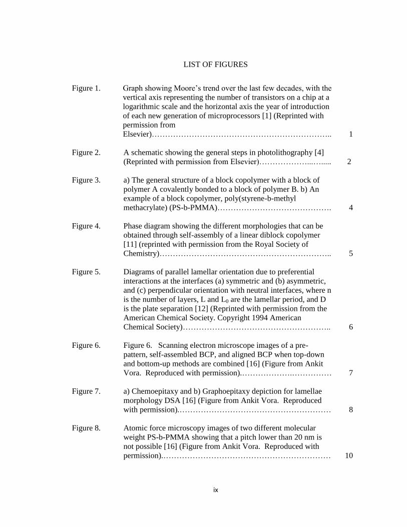
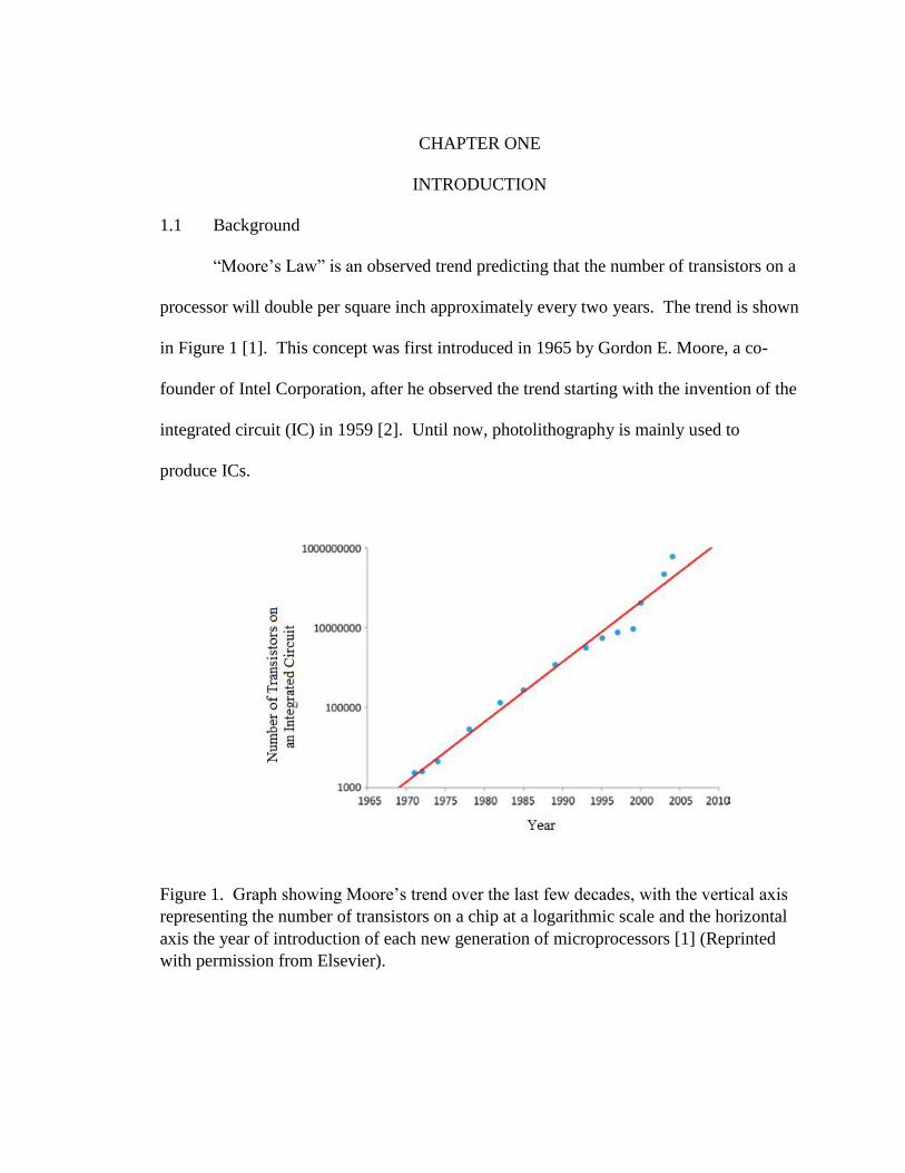
“Moore’s Law” is an observed trend predicting that the number of transistors on a
processor will double per square inch approximately every two years. The trend is shown
in Figure 1 [1]. This concept was first introduced in 1965 by Gordon E. Moore, a co-
founder of Intel Corporation, after he observed the trend starting with the invention of the
integrated circuit (IC) in 1959 [2]. Until now, photolithography is mainly used to
produce ICs.
Figure 1. Graph showing Moore’s trend over the last few decades, with the vertical axis
representing the number of transistors on a chip at a logarithmic scale and the horizontal
axis the year of introduction of each new generation of microprocessors [1] (Reprinted
with permission from Elsevier).
2
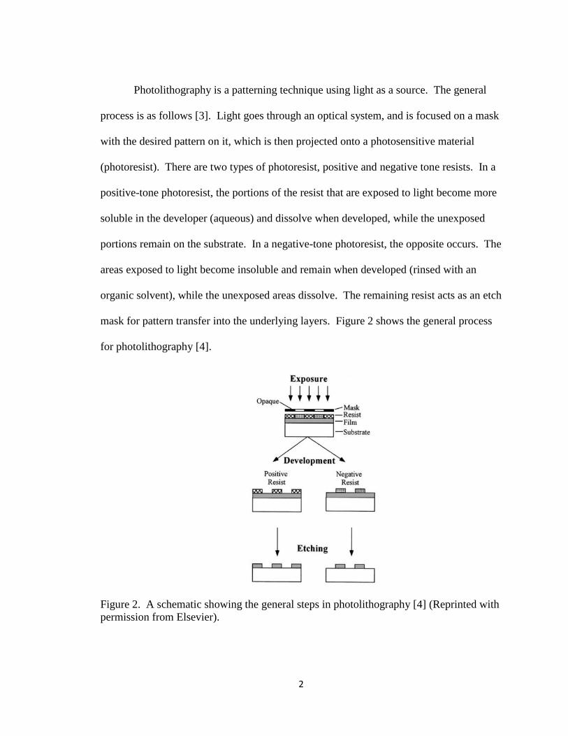
Photolithography is a patterning technique using light as a source. The general
process is as follows [3]. Light goes through an optical system, and is focused on a mask
with the desired pattern on it, which is then projected onto a photosensitive material
(photoresist). There are two types of photoresist, positive and negative tone resists. In a
positive-tone photoresist, the portions of the resist that are exposed to light become more
soluble in the developer (aqueous) and dissolve when developed, while the unexposed
portions remain on the substrate. In a negative-tone photoresist, the opposite occurs. The
areas exposed to light become insoluble and remain when developed (rinsed with an
organic solvent), while the unexposed areas dissolve. The remaining resist acts as an etch
mask for pattern transfer into the underlying layers. Figure 2 shows the general process
for photolithography [4].
Figure 2. A schematic showing the general steps in photolithography [4] (Reprinted with
permission from Elsevier).
3
The size of the pattern features is limited by the wavelength of the light source.
The smaller the wavelength, the smaller feature size can be reached. Over the years, the
industry has progressed from using 436 nm wavelength lithography to the current 193 nm
wavelength immersion lithography (193i), which replaces the air gap between the
substrate surface and final lens with water to increase the refractive index, and therefore
resolution. The 193i wavelength has been used in industry for the past 11 years, with
current pitch limit of 65 nm, extending its use through methods such as multiple
patterning [5]. Multiple patterning, as the name implies, requires multiple lithographic
steps, making the process costly. However, error in the overlay of the mask becomes an
issue and critical dimension control becomes more difficult. Continuing the trend of
Moore’s law of cheaper and smaller ICs is becoming more and more challenging with
current lithography technology.
The wavelength of 13.5 nm available at extreme ultraviolet light (EUV), is one of
the next generation methods in line to continue the trend of Moore’s law. However, the
tool is not yet production ready, and so is unavailable for high volume manufacturing [4-
5]. As such, various alternatives are being investigated to extend current 193i nm
photolithography. One promising candidate is the use of block copolymers (BCPs) for
directed self-assembly (DSA) as a complimentary method with current top-down
photolithography, which was the focus of this study.
1.2 Block Copolymers and Directed Self-Assembly
A copolymer is a polymer that is made of two or more chemically different
polymer chains (noted as A, B, etc.). In a block copolymer, each monomer forms a
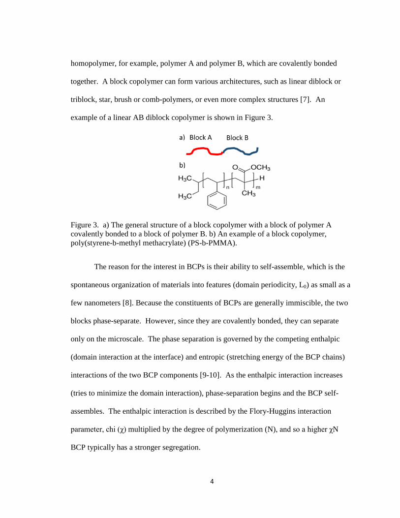
4
homopolymer, for example, polymer A and polymer B, which are covalently bonded
together. A block copolymer can form various architectures, such as linear diblock or
triblock, star, brush or comb-polymers, or even more complex structures [7]. An
example of a linear AB diblock copolymer is shown in Figure 3.
Figure 3. a) The general structure of a block copolymer with a block of polymer A
covalently bonded to a block of polymer B. b) An example of a block copolymer,
poly(styrene-b-methyl methacrylate) (PS-b-PMMA).
The reason for the interest in BCPs is their ability to self-assemble, which is the
spontaneous organization of materials into features (domain periodicity, L0) as small as a
few nanometers [8]. Because the constituents of BCPs are generally immiscible, the two
blocks phase-separate. However, since they are covalently bonded, they can separate
only on the microscale. The phase separation is governed by the competing enthalpic
(domain interaction at the interface) and entropic (stretching energy of the BCP chains)
interactions of the two BCP components [9-10]. As the enthalpic interaction increases
(tries to minimize the domain interaction), phase-separation begins and the BCP self-
assembles. The enthalpic interaction is described by the Flory-Huggins interaction
parameter, chi (χ) multiplied by the degree of polymerization (N), and so a higher χN
BCP typically has a stronger segregation.
5
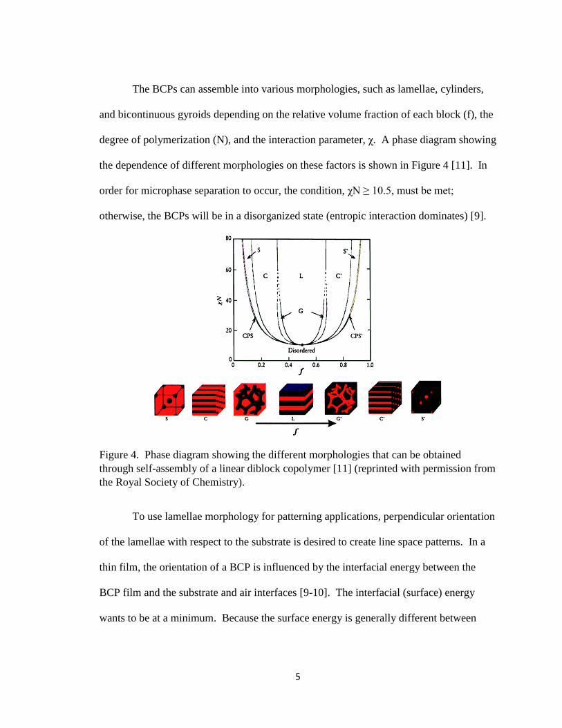
The BCPs can assemble into various morphologies, such as lamellae, cylinders,
and bicontinuous gyroids depending on the relative volume fraction of each block (f), the
degree of polymerization (N), and the interaction parameter, χ. A phase diagram showing
the dependence of different morphologies on these factors is shown in Figure 4 [11]. In
order for microphase separation to occur, the condition, χN ≥ 10.5, must be met;
otherwise, the BCPs will be in a disorganized state (entropic interaction dominates) [9].
Figure 4. Phase diagram showing the different morphologies that can be obtained
through self-assembly of a linear diblock copolymer [11] (reprinted with permission from
the Royal Society of Chemistry).
To use lamellae morphology for patterning applications, perpendicular orientation
of the lamellae with respect to the substrate is desired to create line space patterns. In a
thin film, the orientation of a BCP is influenced by the interfacial energy between the
BCP film and the substrate and air interfaces [9-10]. The interfacial (surface) energy
wants to be at a minimum. Because the surface energy is generally different between
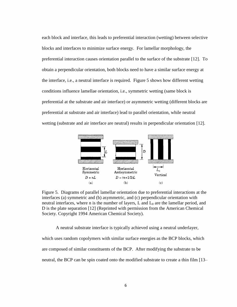
6
each block and interface, this leads to preferential interaction (wetting) between selective
blocks and interfaces to minimize surface energy. For lamellar morphology, the
preferential interaction causes orientation parallel to the surface of the substrate [12]. To
obtain a perpendicular orientation, both blocks need to have a similar surface energy at
the interface, i.e., a neutral interface is required. Figure 5 shows how different wetting
conditions influence lamellae orientation, i.e., symmetric wetting (same block is
preferential at the substrate and air interface) or asymmetric wetting (different blocks are
preferential at substrate and air interface) lead to parallel orientation, while neutral
wetting (substrate and air interface are neutral) results in perpendicular orientation [12].
Figure 5. Diagrams of parallel lamellar orientation due to preferential interactions at the
interfaces (a) symmetric and (b) asymmetric, and (c) perpendicular orientation with
neutral interfaces, where n is the number of layers, L and L0 are the lamellar period, and
D is the plate separation [12] (Reprinted with permission from the American Chemical
Society. Copyright 1994 American Chemical Society).
A neutral substrate interface is typically achieved using a neutral underlayer,
which uses random copolymers with similar surface energies as the BCP blocks, which
are composed of similar constituents of the BCP. After modifying the substrate to be
neutral, the BCP can be spin coated onto the modified substrate to create a thin film [13–
7
15]. The film is then thermally annealed above the Tg (i.e., glass transition) temperature,
but below the decomposition temperature, providing the mobility for the BCP to
reorganize itself into the predicted ordered state [10].
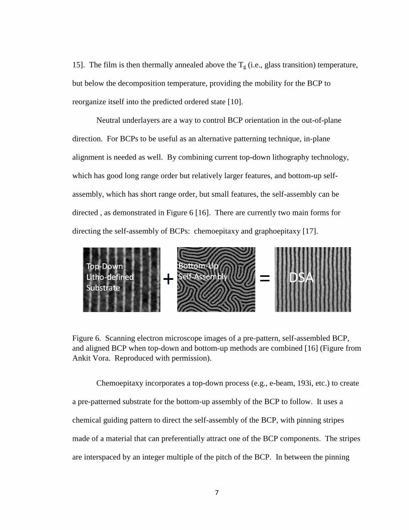
Neutral underlayers are a way to control BCP orientation in the out-of-plane
direction. For BCPs to be useful as an alternative patterning technique, in-plane
alignment is needed as well. By combining current top-down lithography technology,
which has good long range order but relatively larger features, and bottom-up self-
assembly, which has short range order, but small features, the self-assembly can be
directed , as demonstrated in Figure 6 [16]. There are currently two main forms for
directing the self-assembly of BCPs: chemoepitaxy and graphoepitaxy [17].
Figure 6. Scanning electron microscope images of a pre-pattern, self-assembled BCP,
and aligned BCP when top-down and bottom-up methods are combined [16] (Figure from
Ankit Vora. Reproduced with permission).
Chemoepitaxy incorporates a top-down process (e.g., e-beam, 193i, etc.) to create
a pre-patterned substrate for the bottom-up assembly of the BCP to follow. It uses a
chemical guiding pattern to direct the self-assembly of the BCP, with pinning stripes
made of a material that can preferentially attract one of the BCP components. The stripes
are interspaced by an integer multiple of the pitch of the BCP. In between the pinning
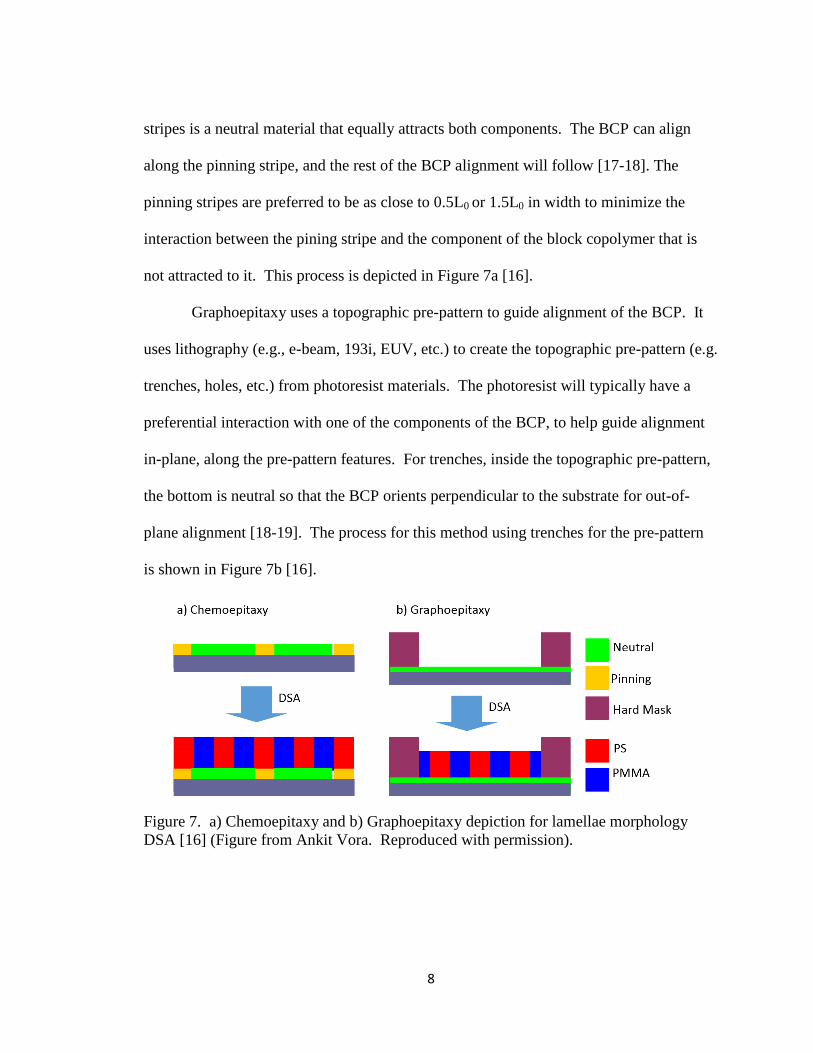
8
stripes is a neutral material that equally attracts both components. The BCP can align
along the pinning stripe, and the rest of the BCP alignment will follow [17-18]. The
pinning stripes are preferred to be as close to 0.5L0 or 1.5L0 in width to minimize the
interaction between the pining stripe and the component of the block copolymer that is
not attracted to it. This process is depicted in Figure 7a [16].
Graphoepitaxy uses a topographic pre-pattern to guide alignment of the BCP. It
uses lithography (e.g., e-beam, 193i, EUV, etc.) to create the topographic pre-pattern (e.g.
trenches, holes, etc.) from photoresist materials. The photoresist will typically have a
preferential interaction with one of the components of the BCP, to help guide alignment
in-plane, along the pre-pattern features. For trenches, inside the topographic pre-pattern,
the bottom is neutral so that the BCP orients perpendicular to the substrate for out-of-
plane alignment [18-19]. The process for this method using trenches for the pre-pattern
is shown in Figure 7b [16].
Figure 7. a) Chemoepitaxy and b) Graphoepitaxy depiction for lamellae morphology
DSA [16] (Figure from Ankit Vora. Reproduced with permission).
9
Once the orientation of the BCP is controlled in and out-of-plane, the thin film
can be used as a patterning template, similar to the role of a photoresist in lithography
[10]. After the BCP morphology and orientation is controlled into a desired pattern
template, one of the block components is removed, typically through an etch process, to
create a mask for pattern transfer.
Currently, PS-b-PMMA is dominantly used for DSA applications in industry.
The structure is shown in Figure 3b. A tremendous amount of research has been done on
PS-b-PMMA for DSA and it is currently the most understood system. It is a readily
available material and has shown to have simple processing conditions ideal for
fabrication processes as it can be spin-coated from fab-friendly solvents (e.g., PGMEA)
and can be thermally annealed [21-22]. Additionally, the surface energies of the two
blocks are balanced at elevated temperatures at the free surface, enabling perpendicular
lamella to form when on a neutral substrate surface. Tsai et al. demonstrated the first 29
nm pitch DSA patterned FinFET device using a process which can easily be integrated
into standard device fabrication [21].
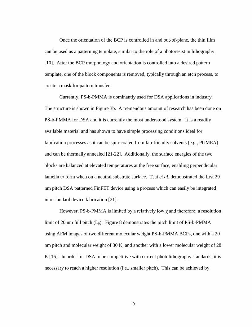
However, PS-b-PMMA is limited by a relatively low χ and therefore; a resolution
limit of 20 nm full pitch (L0). Figure 8 demonstrates the pitch limit of PS-b-PMMA
using AFM images of two different molecular weight PS-b-PMMA BCPs, one with a 20
nm pitch and molecular weight of 30 K, and another with a lower molecular weight of 28
K [16]. In order for DSA to be competitive with current photolithography standards, it is
necessary to reach a higher resolution (i.e., smaller pitch). This can be achieved by
10
controlling the degree of polymerization (N) and the χ parameter. Equation 1 shows the
relationship between χ, N, and L0, where α is a statistical segment length [6].
L0 ≈ αN2/3
χ1/6
Equation 1
By increasing the χ parameter and reducing N, a smaller pitch is possible, making high-χ
BCPs of interest. However, although PS-b-PMMA is inherently neutral at the air
interface, high-χ BCPs are usually not, and so the challenge of using high-χ BCPs is the
difficulty in orientation control at the air interface.
Figure 8. Atomic force microscopy images of two different molecular weight PS-b-
PMMA showing that a pitch lower than 20 nm is not possible [16] (Figure from Ankit
Vora. Reproduced with permission).
1.3 Significance
Lithography is a costly process, especially with the current use of multiple
patterning, requiring multiple lithographic steps to reach sub-20nm features. The ability
of BCPs to self-assemble at the nanoscale make them of interest to use as masks with
current photolithography processes. High-χ BCPs are of particular interest to surpass the
20 nm pitch limit of PS-b-PMMA, which is the dominantly used BCP for DSA in

11
industry. If an orientation control method compatible with fabrication friendly conditions
can be achieved, then high-χ BCPs can be exploited to form nanoscopic features smaller
than those offered by current photolithography processes at a lower cost.
12
CHAPTER TWO
LITERATURE REVIEW
The idea of using block copolymer self-assembly for nanolithographic
applications was first introduced by Mansky in 1995 in a publication, “Monolayer films
of diblock copolymer microdomains for nanolithographic applications [22].” Since then,
a variety of research has been done on self-assembly and DSA. For DSA to be
successful, control of domain orientation of the BCP thin films is crucial. For
perpendicular orientation, it is necessary for the interfaces to be neutral. In this chapter, a
literature overview for methods of orientation control of BCPs and etching methods is
given.
2.1 Neutral Substrate Interface
One of the earlier studies on using random copolymers to modify the substrate
interface was done by Kellogg et al., in which random copolymers consisting of PS and
PMMA (PS-r-PMMA) were coated onto substrate interfaces [23]. This study showed
that as the specific interaction between either block of the BCP and the substrate
decreased, perpendicular orientation was achieved at the substrate interface.
Later on, in 1997, Mansky et al. published a study on using random copolymers
for substrate modification, but instead used hydroxyl (OH) end grafted PS-r-PMMA and
identified surface neutrality through contact angle measurements [24]. The use of the OH
end group on the random copolymer allows the copolymer to end-graft itself to the
silicon oxide layer of the substrate, and therefore immobilizes it. The reason for using
end-grafted polymers was because previously the random copolymer chains were not
13
chemically linked to the substrate, and so the copolymer could diffuse into the BCP film
during annealing.
Mansky et al. showed that when a constant incommensurate film thickness is
used, 1L0 (“classical”) step height features that look like islands or holes are seen at the
surface [25]. Depending on film thickness and whether there is symmetric or
asymmetric wetting, either island or hole topography will be seen. Peter et al. took this a
step further to identify the neutrality of self-assembled monolayers (SAMs) [26]. The
SAM surfaces were oxidized through x-ray radiation with a range of exposures. When a
transition from islands to holes was seen, it was interpreted as a switch of the block that
preferentially wet the substrate.
In 2013, Kim et al. reported a new phenomenon in which 0.5L0 step height
islands and holes were observed [27]. In the study, two different lamella-forming high-χ
BCPs were used, poly(styrene-block-[isoprene-random-epoxysoprene]) (PS-b-PEI78) and
poly(4-trimethylsilelstyrene-block-D,L-lactide) (PTMSS-b-PLA). The BCP, PS-b-
PEI78, is PS-b-PI with 78 mol % epoxidation on the isoprene block which makes the
BCP neutral at the air interface. When PS-b-PI and PS-b-PEI78 were coated onto a PS
brush, which is preferential to the PS block, PS-b-PI formed classical 1L0 step height
features, while PS-b-PEI78 formed 0.5L0 step height features, shown in Figure 9 [27].
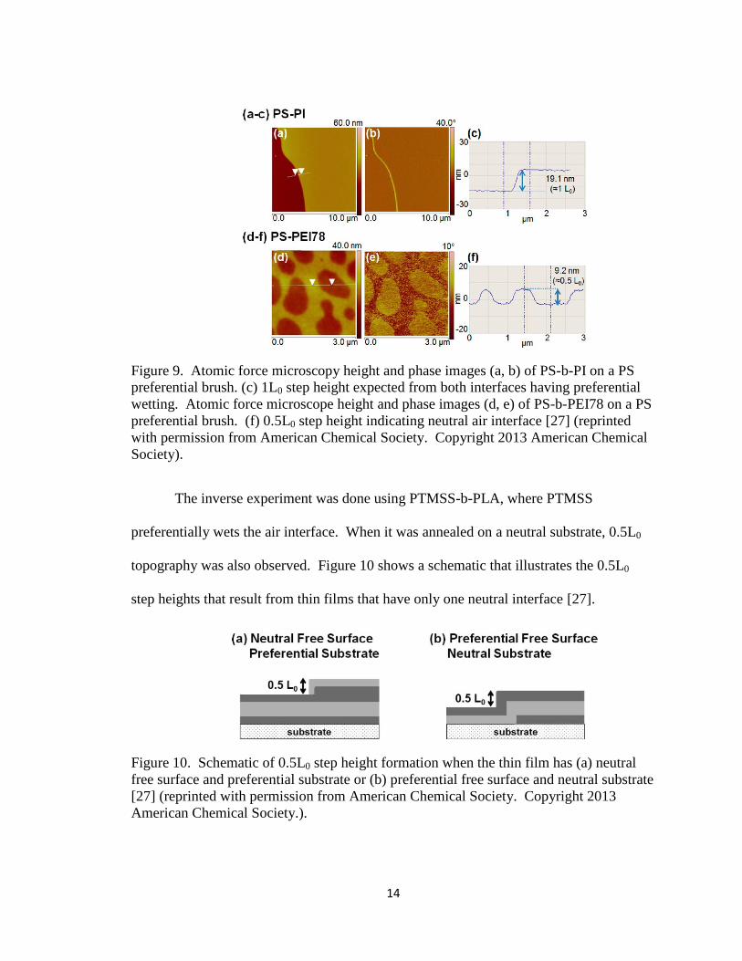
14
Figure 9. Atomic force microscopy height and phase images (a, b) of PS-b-PI on a PS
preferential brush. (c) 1L0 step height expected from both interfaces having preferential
wetting. Atomic force microscope height and phase images (d, e) of PS-b-PEI78 on a PS
preferential brush. (f) 0.5L0 step height indicating neutral air interface [27] (reprinted
with permission from American Chemical Society. Copyright 2013 American Chemical
Society).
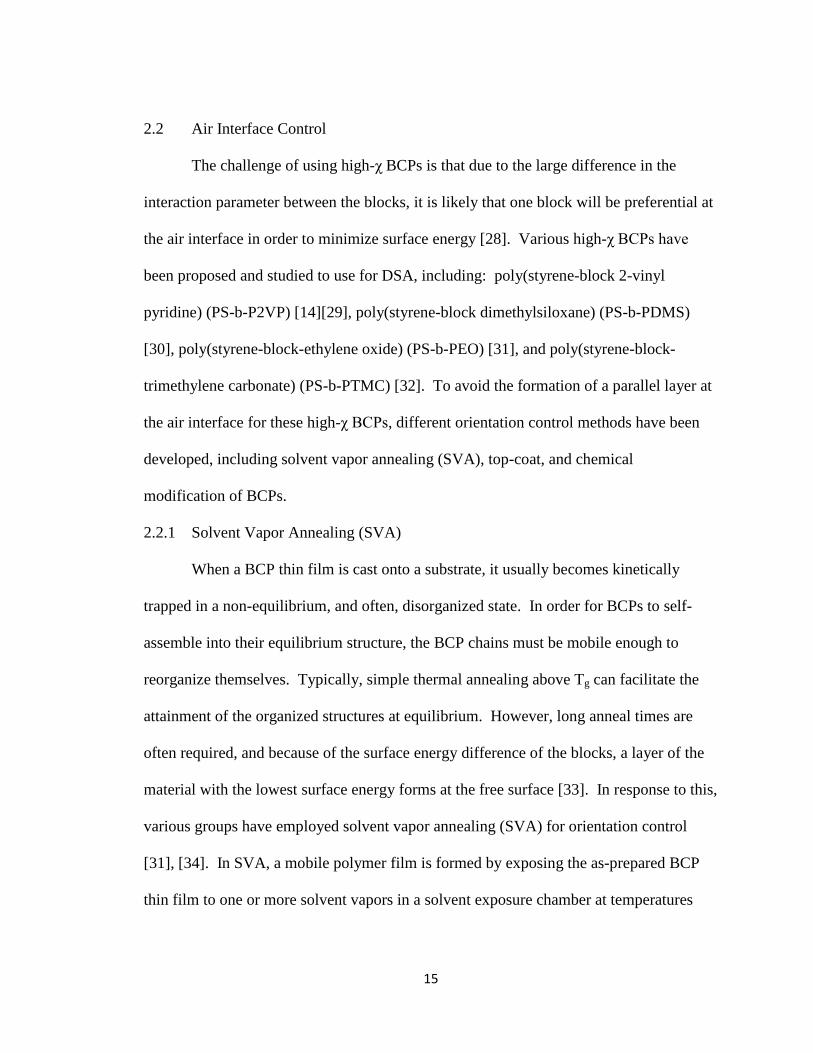
The inverse experiment was done using PTMSS-b-PLA, where PTMSS
preferentially wets the air interface. When it was annealed on a neutral substrate, 0.5L0
topography was also observed. Figure 10 shows a schematic that illustrates the 0.5L0
step heights that result from thin films that have only one neutral interface [27].
Figure 10. Schematic of 0.5L0 step height formation when the thin film has (a) neutral
free surface and preferential substrate or (b) preferential free surface and neutral substrate
[27] (reprinted with permission from American Chemical Society. Copyright 2013
American Chemical Society.).
15
2.2 Air Interface Control
The challenge of using high-χ BCPs is that due to the large difference in the
interaction parameter between the blocks, it is likely that one block will be preferential at
the air interface in order to minimize surface energy [28]. Various high-χ BCPs have
been proposed and studied to use for DSA, including: poly(styrene-block 2-vinyl
pyridine) (PS-b-P2VP) [14][29], poly(styrene-block dimethylsiloxane) (PS-b-PDMS)
[30], poly(styrene-block-ethylene oxide) (PS-b-PEO) [31], and poly(styrene-block-
trimethylene carbonate) (PS-b-PTMC) [32]. To avoid the formation of a parallel layer at
the air interface for these high-χ BCPs, different orientation control methods have been
developed, including solvent vapor annealing (SVA), top-coat, and chemical
modification of BCPs.
2.2.1 Solvent Vapor Annealing (SVA)
When a BCP thin film is cast onto a substrate, it usually becomes kinetically
trapped in a non-equilibrium, and often, disorganized state. In order for BCPs to self-
assemble into their equilibrium structure, the BCP chains must be mobile enough to
reorganize themselves. Typically, simple thermal annealing above Tg can facilitate the
attainment of the organized structures at equilibrium. However, long anneal times are
often required, and because of the surface energy difference of the blocks, a layer of the
material with the lowest surface energy forms at the free surface [33]. In response to this,
various groups have employed solvent vapor annealing (SVA) for orientation control
[31], [34]. In SVA, a mobile polymer film is formed by exposing the as-prepared BCP
thin film to one or more solvent vapors in a solvent exposure chamber at temperatures
16
typically below the Tg of either block [35]. The solvent vapors cause the thin film to
swell and become mobile. Removal of the solvent vapors kinetically traps the polymer,
preserving the orientation. One of the first examples using SVA was completed by
Albalak et al. in 1998 [36]. Since then, SVA has been successfully used for orientation
control of high-χ BCPs, such as PS-b-PDMS [30], PS-b-P2VP [37], and PS-b-PEO [31].
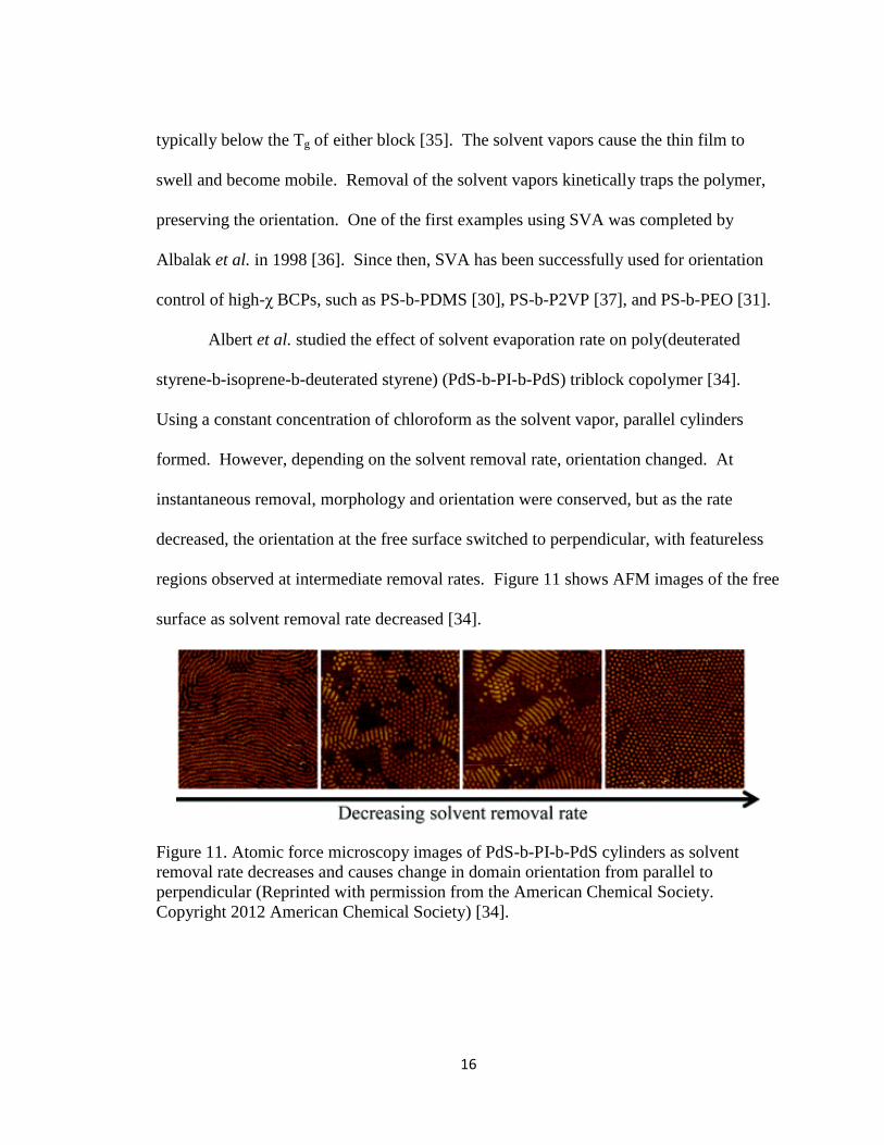
Albert et al. studied the effect of solvent evaporation rate on poly(deuterated
styrene-b-isoprene-b-deuterated styrene) (PdS-b-PI-b-PdS) triblock copolymer [34].
Using a constant concentration of chloroform as the solvent vapor, parallel cylinders
formed. However, depending on the solvent removal rate, orientation changed. At
instantaneous removal, morphology and orientation were conserved, but as the rate
decreased, the orientation at the free surface switched to perpendicular, with featureless
regions observed at intermediate removal rates. Figure 11 shows AFM images of the free
surface as solvent removal rate decreased [34].
Figure 11. Atomic force microscopy images of PdS-b-PI-b-PdS cylinders as solvent
removal rate decreases and causes change in domain orientation from parallel to
perpendicular (Reprinted with permission from the American Chemical Society.
Copyright 2012 American Chemical Society) [34].
17
2.2.2 Top-Coat
A top-coat is compatible with thermal annealing and is meant to work similarly to
the neutral substrate underlayer. A material that is non-preferential for both blocks is
placed on top of the BCP film at the air interface (e.g., spin coat or polymer off-set
printing) so that perpendicular orientation is induced at the air interface with the use of
thermal annealing [13-14]. The use of top-coats has been successful on high-χ BCPs
such as PTMSS-b-PLA [13] and PS-b-P2VP [14].
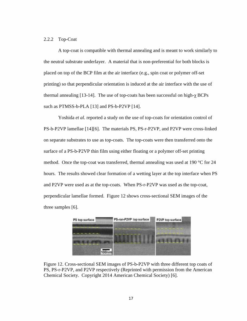
Yoshida et al. reported a study on the use of top-coats for orientation control of
PS-b-P2VP lamellae [14][6]. The materials PS, PS-r-P2VP, and P2VP were cross-linked
on separate substrates to use as top-coats. The top-coats were then transferred onto the
surface of a PS-b-P2VP thin film using either floating or a polymer off-set printing
method. Once the top-coat was transferred, thermal annealing was used at 190 °C for 24
hours. The results showed clear formation of a wetting layer at the top interface when PS
and P2VP were used as at the top-coats. When PS-r-P2VP was used as the top-coat,
perpendicular lamellae formed. Figure 12 shows cross-sectional SEM images of the
three samples [6].
Figure 12. Cross-sectional SEM images of PS-b-P2VP with three different top coats of
PS, PS-r-P2VP, and P2VP respectively (Reprinted with permission from the American
Chemical Society. Copyright 2014 American Chemical Society) [6].
18
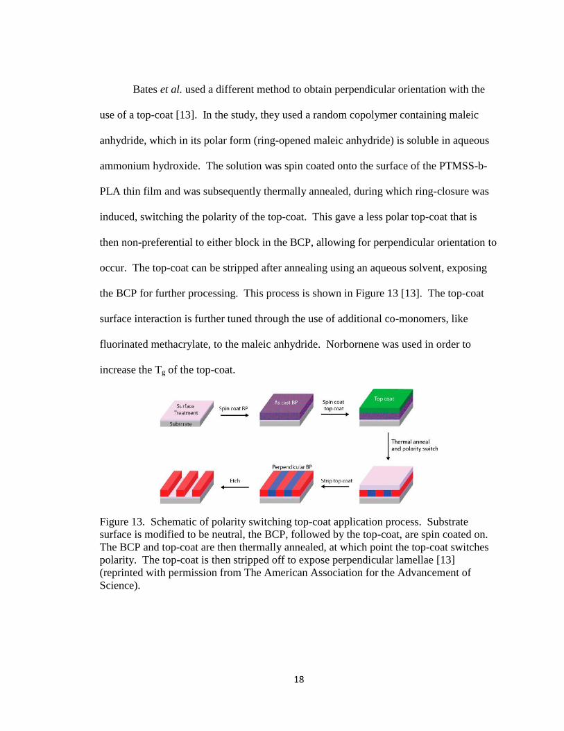
Bates et al. used a different method to obtain perpendicular orientation with the
use of a top-coat [13]. In the study, they used a random copolymer containing maleic
anhydride, which in its polar form (ring-opened maleic anhydride) is soluble in aqueous
ammonium hydroxide. The solution was spin coated onto the surface of the PTMSS-b-
PLA thin film and was subsequently thermally annealed, during which ring-closure was
induced, switching the polarity of the top-coat. This gave a less polar top-coat that is
then non-preferential to either block in the BCP, allowing for perpendicular orientation to
occur. The top-coat can be stripped after annealing using an aqueous solvent, exposing
the BCP for further processing. This process is shown in Figure 13 [13]. The top-coat
surface interaction is further tuned through the use of additional co-monomers, like
fluorinated methacrylate, to the maleic anhydride. Norbornene was used in order to
increase the Tg of the top-coat.
Figure 13. Schematic of polarity switching top-coat application process. Substrate
surface is modified to be neutral, the BCP, followed by the top-coat, are spin coated on.
The BCP and top-coat are then thermally annealed, at which point the top-coat switches
polarity. The top-coat is then stripped off to expose perpendicular lamellae [13]
(reprinted with permission from The American Association for the Advancement of
Science).
19
The floating method for applying a top-coat suffers from scalability issues and
introduction of defects [38]. Additionally, neutral polymers spin coated onto the BCP
tend to be soluble in a solvent that dissolves the BCP, making removal of the top-coat a
challenge. Although Bates et al. surpassed these challenges with the polarity switching
top-coat, the process still requires an additional spin coating step and removal step [13].
2.2.3 Selective Chemical Modification
Though both SVA and top-coat methods have been shown to induce
perpendicular orientation, it would be beneficial to use BCPs that are non-preferential at
the air interface and do not require any additional processing steps. Some examples of
such BCPs include PS-b-PLA [39], poly(ethylene glycol-b-fluorinated methacrylate)
[40], and PS-b-PEI78 [15]. However, design of such BCPs is challenging.
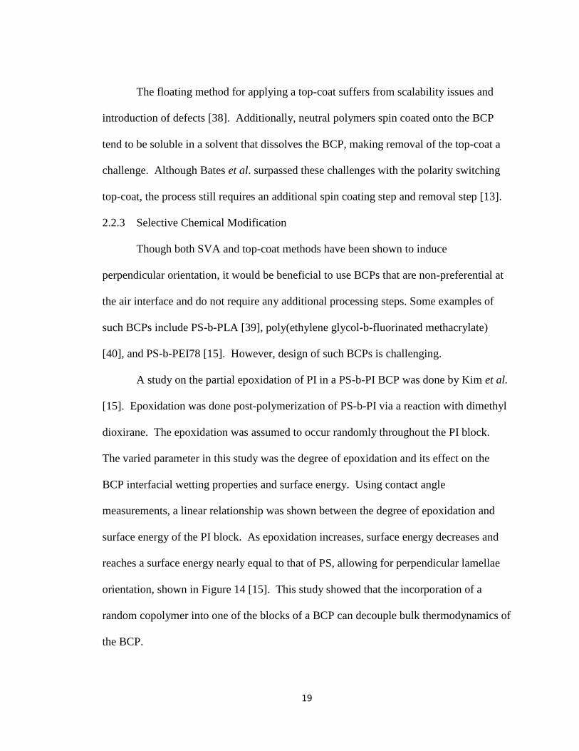
A study on the partial epoxidation of PI in a PS-b-PI BCP was done by Kim et al.
[15]. Epoxidation was done post-polymerization of PS-b-PI via a reaction with dimethyl
dioxirane. The epoxidation was assumed to occur randomly throughout the PI block.
The varied parameter in this study was the degree of epoxidation and its effect on the
BCP interfacial wetting properties and surface energy. Using contact angle
measurements, a linear relationship was shown between the degree of epoxidation and
surface energy of the PI block. As epoxidation increases, surface energy decreases and
reaches a surface energy nearly equal to that of PS, allowing for perpendicular lamellae
orientation, shown in Figure 14 [15]. This study showed that the incorporation of a
random copolymer into one of the blocks of a BCP can decouple bulk thermodynamics of
the BCP.
20
Figure 14. Scanning electron microscope images of PS-PI as the degree of epoxidation
increases on the PI block, showing PS-PI can be converted to a BCP with equal surface
energies of the blocks [15] (reprinted with permission from the American Chemical
Society. Copyright 2012 American Chemical Society).
2.2.4 Embedded Neutral Layer
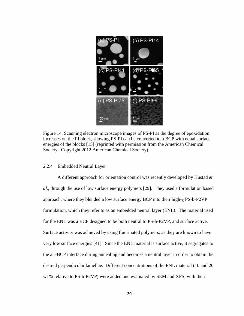
A different approach for orientation control was recently developed by Hustad et
al., through the use of low surface energy polymers [29]. They used a formulation based
approach, where they blended a low surface energy BCP into their high-χ PS-b-P2VP
formulation, which they refer to as an embedded neutral layer (ENL). The material used
for the ENL was a BCP designed to be both neutral to PS-b-P2VP, and surface active.
Surface activity was achieved by using fluorinated polymers, as they are known to have
very low surface energies [41]. Since the ENL material is surface active, it segregates to
the air-BCP interface during annealing and becomes a neutral layer in order to obtain the
desired perpendicular lamellae. Different concentrations of the ENL material (10 and 20
wt % relative to PS-b-P2VP) were added and evaluated by SEM and XPS, with their
21
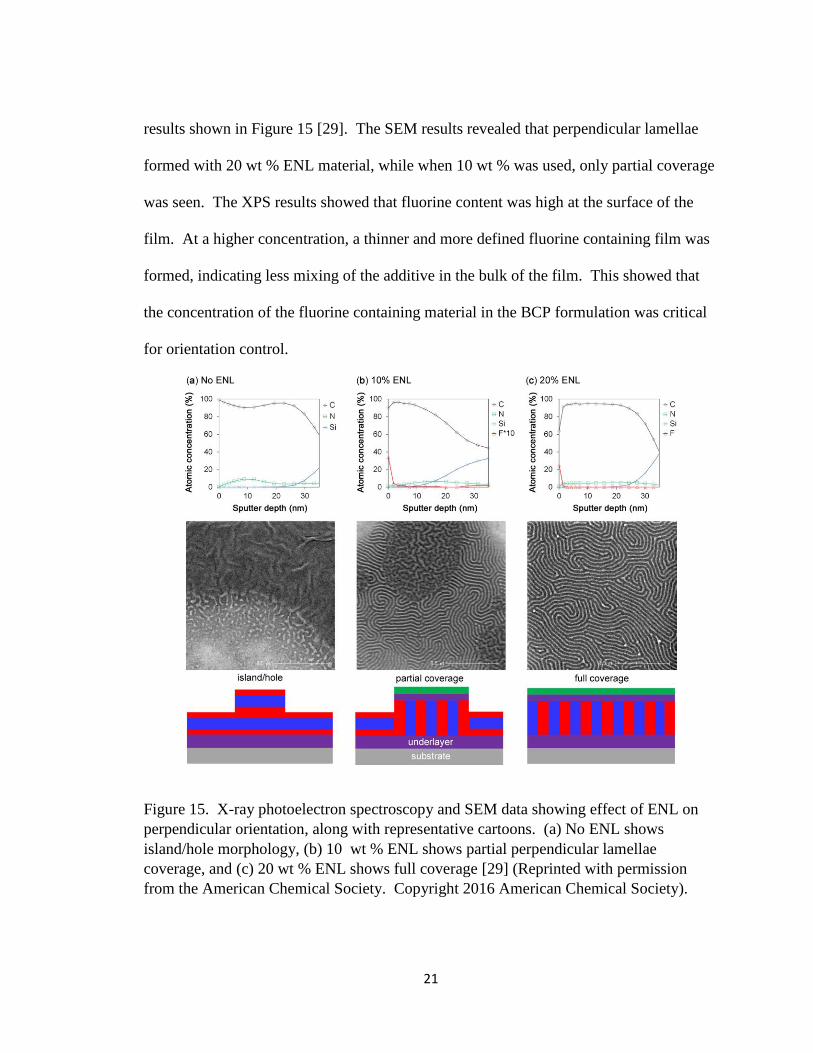
results shown in Figure 15 [29]. The SEM results revealed that perpendicular lamellae
formed with 20 wt % ENL material, while when 10 wt % was used, only partial coverage
was seen. The XPS results showed that fluorine content was high at the surface of the
film. At a higher concentration, a thinner and more defined fluorine containing film was
formed, indicating less mixing of the additive in the bulk of the film. This showed that
the concentration of the fluorine containing material in the BCP formulation was critical
for orientation control.
Figure 15. X-ray photoelectron spectroscopy and SEM data showing effect of ENL on
perpendicular orientation, along with representative cartoons. (a) No ENL shows
island/hole morphology, (b) 10 wt % ENL shows partial perpendicular lamellae
coverage, and (c) 20 wt % ENL shows full coverage [29] (Reprinted with permission
from the American Chemical Society. Copyright 2016 American Chemical Society).
22
2.3 Etch Processes
For DSA to be successfully implemented as an alternative to current multiple
patterning processes, pattern transfer is essential. Reactive ion etching (RIE) is a
commonly used process for pattern transfer to selectively remove one of the blocks [31-
32], [43-44]. Synthesizing BCPs with one etch-resistant block has been one of the
strategies focused on by many groups in order to increase etch selectivity for reactive ion
etching (RIE) [6]. Typically, the etch resistant block has an inorganic component, such
as silicon. A reason Bates et al. selected PTMSS-b-PLA for their top-coat study, was
because PTMSS (silicon-containing block) has a much lower O2 RIE rate than PLA [13].
Another high-χ BCP, PS-b-PDMS, has also been of interest due to the high etch
selectivity between the blocks due to the silicon containing block (PDMS) [30].
An alternative approach to increase etch contrast, is the use of sequential
infiltration synthesis (SIS). The SIS experiment is carried out in an atomic layer
deposition (ALD) chamber, where a material of interest nucleates within the polymer
bulk, and these sites then serve as seeds for growth of inorganic particles [44]. Tseng et
al. used gas-phase tri-methyl aluminum (TMA) to diffuse through a PS-b-PMMA film
and selectively grow in the PMMA domains due to a chemical interaction between TMA
and the carbonyl group in PMMA [45]. The process was done via an exposure/purge
process in an ALD chamber using TMA and water [44-45]. The presence of the
inorganic component, in that case, aluminum oxide, in the PMMA domain made it
significantly more etch resistive than PS.
23
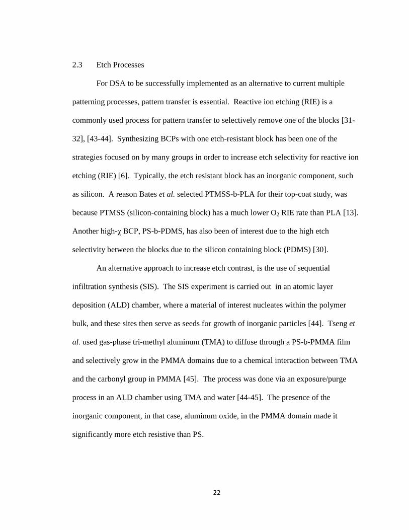
In a study done by Gokan et al. the dry etch resistance for organic molecules was
investigated [46]. Using oxygen-ion etching, they looked at various organic polymers,
with particular attention to the carbon and oxygen content in the polymer structure.
Carbon was reported to be the rate-determining step in the etch rate, while an increased
oxygen content in the polymer structure gave higher etching rates. They found a linear
correlation between etch rate and oxygen and carbon content in organic polymers given
in Equation 2 [46]
𝑉 ∝ 𝑁
𝑁𝐶−𝑁𝑂 Equation 2
where V is the etch rate, N is the total number of atoms in a monomer unit, NC is the total
number of carbon atoms in a monomer unit, and NO is the total number of oxygen atoms
in a monomer unit. This means that organic polymers with a high ratio of oxygen to
carbon atoms will have a higher etch rate than polymers consisting of mostly carbon.
2.4 Summary
Based on previous research, it is now widely known that using end grafted
random copolymers consisting of the same or similar constituents as the BCP can be used
to modify the substrate surface to yield a neutral surface. With the work done by Kim et
al., the composition of the random copolymer needed to obtain a neutral substrate surface
can be easily recognized through the use of AFM by identifying which composition
forms 0.5L0 step height features [27].
Currently, there are three main methods for orientation control of the air-BCP
interface: SVA, top-coats, and chemical modification. For SVA, the literature showed
that various parameters need to be controlled, and very volatile solvents (e.g., chloroform
24
and THF) are typically used in the process [36-37]. Top-coats are compatible with the
thermal annealing process, but still require additional processing steps in comparison to
PS-b-PMMA [13-14]. More recently, the use of surface active polymers, particularly
fluorinated polymers, have become of interest. When using surface active polymers,
concentration is an important parameter to consider, as an insufficient amount does not
allow for full coverage of perpendicular lamellae on the surface.
To selectively remove one of the blocks of the BCP, the two BCP constituents
must have significantly different RIE rates. Using silicon-containing BCPs has been
reported to increase etch selectivity [13], [30]. Use of SIS is another reported method,
most commonly done using TMA and water, where the TMA selectively interacts with
functional groups, such as carbonyls [43-44]. For organic BCPs, Gokan et al. showed
that a high oxygen to carbon ratio is desired [46].
25
CHAPTER THREE
OBJECTIVE AND HYPOTHESIS
3.1 Objective and Justification
For this study, a carbonate platform BCP, poly(styrene-b-methyl 5-methyl-2-oxo-
1,3-dioxane-5-carboxylate) (PS-b-PMeCAR), was chosen as a high-χ BCP for sub-20 nm
pitch patterning. Various cyclic carbonate monomers can be polymerized by ring-
opening polymerization from a hydroxyl-end function PS macroinitiator in order to tune
the χ parameter to PS. Depending on the carbonate monomers used, these carbonate
based BCPs can be high-χ systems. In addition, PMeCAR is expected to have a higher
RIE rate due to the high oxygen to carbon ratio of the monomer unit in comparison to PS.
Because of the polarity difference between the two block components, they have different
surface energies, causing preferential interactions at the substrate and the air interfaces,
and therefore an orientation control strategy is needed to enable vertically orientated BCP
domains.
The objective of this study was to show how surface active polymers (SAP) as
additives can be used to control the orientation of BCPs at the air interface. The SAPs
consist of fluorinated groups to achieve a low surface energy, and an alcohol group that
allows hydrogen bonding to occur preferentially between the SAP and a functional group
in the higher surface energy block, i.e., carbonyl block [40-41]. Once bonded, the SAP is
expected to pull this block towards the surface so that both blocks will be at the air
interface.
26
The goal of this study was to optimize the BCP and SAP system to find
fabrication friendly process conditions (e.g., short thermal anneal time, spin coat from
conventional solvents, no topcoat, etc.) for enabling perpendicular orientation of the
BCP. This was done by analyzing the effect of different SAP compositions and
concentrations on the high-χ BCP orientation using AFM, SEM, and GISAXS. The SAP
location in the film was verified using XPS. In addition, film thickness and etch studies
with and without sequential infiltration synthesis (SIS) were done. The other objective
was to successfully demonstrate DSA using graphoepitaxy. Temperature and annealing
time were adjusted to improve alignment.
3.2 Motivation
Current methods of orientation control for high-χ BCPs with sub-20 nm pitch all
have their drawbacks in comparison to the more fabrication-friendly method used for PS-
b-PMMA, such as:
The solvents used for solvent vapor annealing (SVA) are not fabrication friendly.
Top-coats require additional processing steps in comparison to PS-b-PMMA.
Block copolymers inherently neutral at the air interface are challenging to design.
Embedded neutral layer (ENL) requires a high dose of the surface active neutral
polymer, which could change the effective volume fraction of the BCP domains
and negatively influence the etch selectivity.

27
The use of SAP as additives (i.e., less than 5 wt % relative to the BCP solids) is a
formulation-based method compatible with thermal annealing and without additional
processing steps, making the method fabrication-friendly.
28
CHAPTER FOUR
MATERIALS AND METHODS
In this chapter, the materials, methods, and experimental details used to determine
which SAP composition and concentration are ideal for orientation control of the PS-b-
PMeCAR BCP to obtain perpendicular lamellae will be specified. As explained in the
introduction chapter, neutral substrate and air interfaces are required to obtain
perpendicular lamellae orientation. Therefore, identification of a neutral underlayer is an
important first step for orientation control. For BCPs with SAP additive formulations to
be implemented in fabrication processes, successful DSA (i.e., defect-free long range
order) and the ability to selectively remove a BCP domain have to be demonstrated.
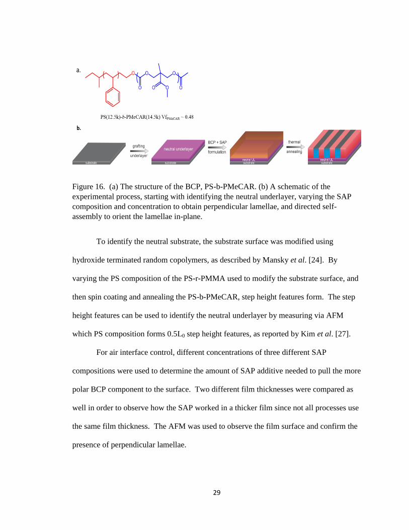
Table 1 presents a summary of the main experiments carried out, while Figure 16 shows
the structure of PS-b-PMeCAR and a schematic of the process.
Table 1. Summary of experiments for orientation control of BCP thin film and DSA.
Step Type of
experiments
Parameters Values Characterization
Neutral
Substrate
Interface
Spin coating of
PS-r-PMMA
Variation of PS
composition 0-32 % PS
AFM (Step
height
measurements)
Control of
Air
Interface
Spin coating of
PS-b-
PMeCAR +
SAP
SAP composition
SAP 1
SAP 2-40
SAP 2-80 AFM
GISAXS
XPS SAP
concentration 2-3 wt %
Film thickness 30-40 nm
Directed
Self
Assembly
Graphoepitaxy
Temperature
170 °C
200 °C SEM
Time 5 min
10 min
29
Figure 16. (a) The structure of the BCP, PS-b-PMeCAR. (b) A schematic of the
experimental process, starting with identifying the neutral underlayer, varying the SAP
composition and concentration to obtain perpendicular lamellae, and directed self-
assembly to orient the lamellae in-plane.
To identify the neutral substrate, the substrate surface was modified using
hydroxide terminated random copolymers, as described by Mansky et al. [24]. By
varying the PS composition of the PS-r-PMMA used to modify the substrate surface, and
then spin coating and annealing the PS-b-PMeCAR, step height features form. The step
height features can be used to identify the neutral underlayer by measuring via AFM
which PS composition forms 0.5L0 step height features, as reported by Kim et al. [27].
For air interface control, different concentrations of three different SAP
compositions were used to determine the amount of SAP additive needed to pull the more
polar BCP component to the surface. Two different film thicknesses were compared as
well in order to observe how the SAP worked in a thicker film since not all processes use
the same film thickness. The AFM was used to observe the film surface and confirm the
presence of perpendicular lamellae.
30
A reactive ion etch (RIE) process and a sequential infiltration synthesis (SIS)
process were applied to thin film samples with successful perpendicular orientation to
show that they can be successfully used to selectively remove a BCP domain.
Demonstration that a domain can be selectively removed is important to show in order for
SAP additives to be considered for patterning applications.
As stated in the introduction, along with out-of-plane orientation control, in-plane
alignment is also important for the use of BCPs in patterning applications. For the DSA
step, graphoepitaxy was attempted on a SAP additive containing BCP formulation that
showed successful perpendicular orientation. However, because the initial annealing
conditions used did not give satisfactory results, temperature and time were varied to
improve the alignment [48]. To check the BCP alignment along the pre-pattern, SEM
was used.
4.1 Materials
The PS-b-PMeCAR BCP, and SAP additives used were synthesized at IBM
Research-Almaden. The properties of PS-b-PMeCAR are as follows: MnPS = 12,500
g/mol, MnPMeCAR = 14,500 g/mol, volume fraction of PMeCAR block, VfPMeCAR ~ 0.48,
and PDI = 1.02.
The PS-r-PMMA random copolymers are hydroxyl-end functionalized in order to
graft onto the silicon substrate and were used as underlayers. The PS-r-PMMA solutions
consisting of 0 and 20% styrene were provided by EMD Performance Materials
Corporation (AZEMBLYTM
NLD-303 and AZEMBLYTM
NLD-328J, respectively). The
PS-r-PMMA solution consisting of 32% styrene was synthesized at IBM.
31
4.2 Methods
4.2.1 Preparation of Underlayer Solution
For the 32% styrene underlayer solution prepared on site at IBM, the PS-r-PMMA
copolymer was obtained in powder form. The copolymer solution was made by
dissolving the powder PS-r-PMMA in PGMEA, to make a 1.0 wt % with a 95:5 weight
ratio of PS-r-PMMA to PNBT. To remove particles, the underlayer solution was filtered
through a 0.2 μm nylon filter. The 0 and 20% styrene solutions were used as received,
and did not require filtering, as they were already filtered.
4.2.2 Preparation of BCP solution and SAP formulations
The PS-b-PMeCAR, was obtained in powder form, and was synthesized using the
method described by Vora et al. for ring opening polymerization of carbonates from PS-
OH [32]. The powder was dissolved in PGMEA, to create a 1.2 wt % solution. To
prepare the BCP with SAP additive formulations, a 1.2 wt % stock solution of the SAP in
PGMEA was used, and 2-3 wt % of SAP stock solution was added to the BCP stock
solution. Once fully dissolved, the solution was passed through a 0.2 μm nylon filter to
remove particles.
4.2.3 Identification of Neutral Underlayer
Hydroxyl terminated PS-r-PMMA solutions of varying ratios of styrene and
methyl methacrylate were grafted onto bare silicon by spin coating at 2000 rpm for 30
seconds and subsequently annealed. For the underlayer solutions prepared at IBM, the
substrate was annealed at 200 °C for 3 minutes. For the underlayer solutions provided by
32
EMD Performance Materials Corporation, the substrates were annealed at 250 °C for 2
minutes.
The substrates were rinsed with PGMEA to remove any unreacted material. This
was done by spin coating the PGMEA on the substrates at 2000 rpm for 30 seconds.
Afterwards, the BCP solution without any SAP was spin coated at 2000 rpm for 30
seconds. The samples were annealed at 170 °C for 5 minutes which is well above the Tg
temperature of PS (which has the higher Tg of the two BCP components at about 100 °C).
The thin films were characterized by AFM to measure the step height of the islands and
holes. Using the method proposed by Kim et al., an underlayer that showed a step height
of 0.5L0 was selected as the neutral underlayer [27].
4.2.4 Thin Film Sample Preparation
The neutral underlayer was applied onto the silicon substrate under the same
conditions described above. After rinsing with PGMEA to remove any unreacted
material, the BCP with SAP additive formulation was spin coated between 1500-2000
rpm, depending on desired film thickness, for 30 seconds. The sample was annealed at
170 °C for 5 minutes. The surface topography was analyzed using AFM. The AFM was
used to determine orientation of the lamellae. Additional analysis of the thin film was
done using GISAXS and XPS.
4.2.5 Preparation of Graphoepitaxy Pre-pattern
AZEMBLY™ NLD-328J (20% PS) was spin coated at 2000 rpm for 30 seconds
on a silicon wafer substrate stack comprised of a silicon wafer bottom layer coated with
~30 nm thick amorphous carbon layer and 10 nm thick silicon nitride (SiNx) layer. After
33
forming the thin film, the coated wafer was baked at 250 °C for 2 minutes and cooled to
room temperature. The underlayer was then given a solvent rinse by casting PGMEA on
top of the coated wafer, letting the solvent puddle for 30 seconds, and spin drying the
treated wafer at 2000 rpm for 30 seconds. The final film thickness of the underlayer was
10 nm after the solvent rinse. Next, a 60 nm thick layer of a commercial 193 nm
negative-tone photoresist (JSR ARF7210JN-8) was disposed on this underlayer coated
substrate followed by post application bake at 80 °C for 60 seconds. The photoresist
layer was then exposed using a 193 nm immersion interference tool (IBM NEMO) with
fixed dose of 4.67 mJ, baked at 95 °C for 60 seconds, and developed for 60 seconds with
2-heptanone developer. The resulting 200 nm pitch patterned photoresist layer was then
hard baked at 200 °C for 3 minutes prior to coating a block copolymer formulation.
4.2.6 Preparation of Graphoepitaxy DSA Samples
PS-b-PMeCAR BCP was dissolved in PGMEA to form a 0.8 wt % stock solution
based on total weight of the solution. A separate 0.8 wt % stock solution of the selected
SAP in PGMEA was prepared. The desired amount of SAP stock solution was added to
the BCP solution and stirred to form a homogeneous solution. The BCP with SAP
additive formulation was passed through a 0.2 μm nylon filter to remove particles.
The formulation was spin coated onto the pre-patterned substrate described in the
previous section at 2000 rpm for 30 seconds. It was subsequently thermal annealed at the
desired temperature and time, and immediately cooled to room temperature. Alignment
and defectivity inside the guiding pre-pattern trenches was determined using top-down
SEM.
34
4.2.7 SIS Process
A thin film of the BCP was placed in a Cambridge NanoTech Fiji F200 at 75 °C.
Trimethyl aluminum (TMA) was admitted into the reactor at a pressure of 70 Torr for 5
minutes. The chamber was evacuated to a pressure below 20 mTorr to remove excess
TMA and byproducts. Water was then introduced at a pressure of 70 Torr for 5 minutes
and then purged to complete the cycle. The process was repeated for 7 cycles.
4.2.8 Etch Process
Etching experiments without SIS were done on a trilayer stack consisting of a
silicon substrate, followed by α-carbon (30 nm), SiNx (10 nm), and the underlayer. To
remove the PMeCAR but preserve the PS, an O2 etch was used in a Lam Research 4520
XLe dielectric etcher. The following parameters were used: 7 sec, 300 mTorr, O2 flow
rate of 136 sccm, lower electrode power 50 W, upper electrode power 0 W, and gap
between electrodes 2.25 cm. To remove SiNX, a mixture of CF4 and CHF3 was used by a
Plasma Therm Versaline ICP etcher. The following parameters were used: 13 sec, 4
mTorr, CF4 flow rate of 20 sccm, CHF3 flow rate of 15 sccm, bias power 50 W, and coil
power 100 W. To remove the α-carbon, a mixture of O2 and N2 was used in the same
etcher as for SiNX. The following parameters were used for this step: 30 sec, 4 mTorr,
O2 flow rate 2 sccm, N2 flow rate 40 sccm, bias power 100 W, and coil power 200 W.
The etch process for the SIS modified sample was done with a Lam Research
4520 XLe dielectric etch tool. To remove the PS domain, the following parameters were
used: 10 sec, 500 mTorr, O2 flow rate of 136 sccm, lower electrode power 50 W, upper
35
electrode power 0 W, and gap between electrodes 2.25 cm. All of the samples post etch
process were imaged using a Leo Gemini SEM to characterize the morphology.
4.3 Instrumentation
4.3.1 AFM
A Digital Instruments 3100 AFM operated in tapping mode in air using a Si
cantilever with a 1 N/m spring constant was used to analyze the surface topography of the
BCP thin films. The typical scan rate used was 1 Hz, with image sizes varying from
2 μm x 2 μm to 5 μm x 5 μm. The 5 μm x 5 μm scan size was used to measure step
height differences to identify the neutral underlayer, while the 2 μm x 2 μm scan sizes
were used to determine the orientation of the lamellae and to measure the pitch of the
BCP. The step height measurements were done using the section cut, and the pitch
measurements were done using the section and power spectral density features on the
Nanoscope Analysis v. 1.5 AFM software by Bruker.
4.3.2 SEM
A Leo Gemini scanning electron microscope (SEM) at 10.0 kV electron charge
was used to measure the DSA samples. For top-down images of the samples throughout
the etch process, a 100k magnification was used. A 200k magnification was used to take
the images of the post-etch cross-sections, graphoepitaxy pre-pattern, and DSA samples.
4.3.3 GISAXS
Grazing incidence small angle X-ray scattering (GISAXS) was used to analyze
lamellae orientation over a larger area and throughout the film of a sample. The GISAXS
data was collected at the Advanced Light Source (ALS) at Lawrence Berkeley National
36
Laboratory (LBNL) at beam line 7.3.3 [49]. The incident X-ray energy was 10 keV and
the sample to detector distance was 4 m. Scattered X-rays were collected using a Pilatus
2M detector. Data was normalized for incoming x-ray intensity, film thickness and wafer
size, averaged, and integrated along qx = 0.028 Å-1
using the IRENA package, developed
by I. Ilavsky et al. [50]. The scattering profiles were analyzed by fitting a series of Voigt
peaks and an exponential background to the 1D data. The periodicity was calculated from
the 1st order Bragg peak by d = 2π/q, where d is the periodicity and q is the scattering
wave vector.
4.3.4 XPS
X-ray photoelectron spectroscopy (XPS) analysis was done on a Physical
Electronics Quantum ESCA Microprobe, using a monochromated AlKaX-ray source at
187.85 eV, 200 μm spot size throughout, and charge neutralization. High resolution
spectra were taken at three different angles for depth profiling: 15° (47 eV PE, 0.4
eV/step, electron escape depth ~ 3 nm), 45° (59 eV PE, 0.4 eV/step, electron escape
depth ~ 8 nm), and 80° (24 eV PE, 0.2 eV/step, electron escape depth ~ 12 nm).
37
CHAPTER FIVE
RESULTS AND DISCUSSION
The results obtained for self-assembly and DSA using a high-χ BCP based on a
polycarbonate platform are discussed in this chapter. The discussion is divided into
sections in sequential order, starting with identification of a neutral underlayer, followed
by orientation control using different SAP additives, etch and SIS results, and then
alignment using graphoepitaxy DSA.
5.1 Random Copolymer as Neutral Underlayer
As the first step to control the orientation of the PS-b-PMeCAR lamellae, a
neutral underlayer was identified. For thermally annealed systems, a non-preferential
substrate interface can be obtained by grafting random copolymers onto the substrate.
For PS-b-PMeCAR, hydroxyl end-functional PS-r-PMMA copolymer brushes with
varying amounts of PS were chosen to modify the substrate interface. To identify which
composition is neutral for the BCP, a qualitative method previously presented by Kim et
al. was used, in which the formation of 0.5L0 island or hole step height features appear
when only one interface is neutral [27]. For PS-b-PMeCAR, polystyrene has the lower
surface energy of the two BCP components, and therefore is expected to be the only
material at the air-BCP interface, making the air-BCP interface non-neutral [32]. If the
random copolymer brush is non-neutral, then 1L0 step height features form, whereas
0.5L0 step height features form only if the random copolymer brush is neutral. The step
heights were measured by AFM. Using a PMMA brush (0% S), the AFM image shown
in Figure 17a, shows hole morphology with approximately 1L0 step height (L = 18.9 nm).
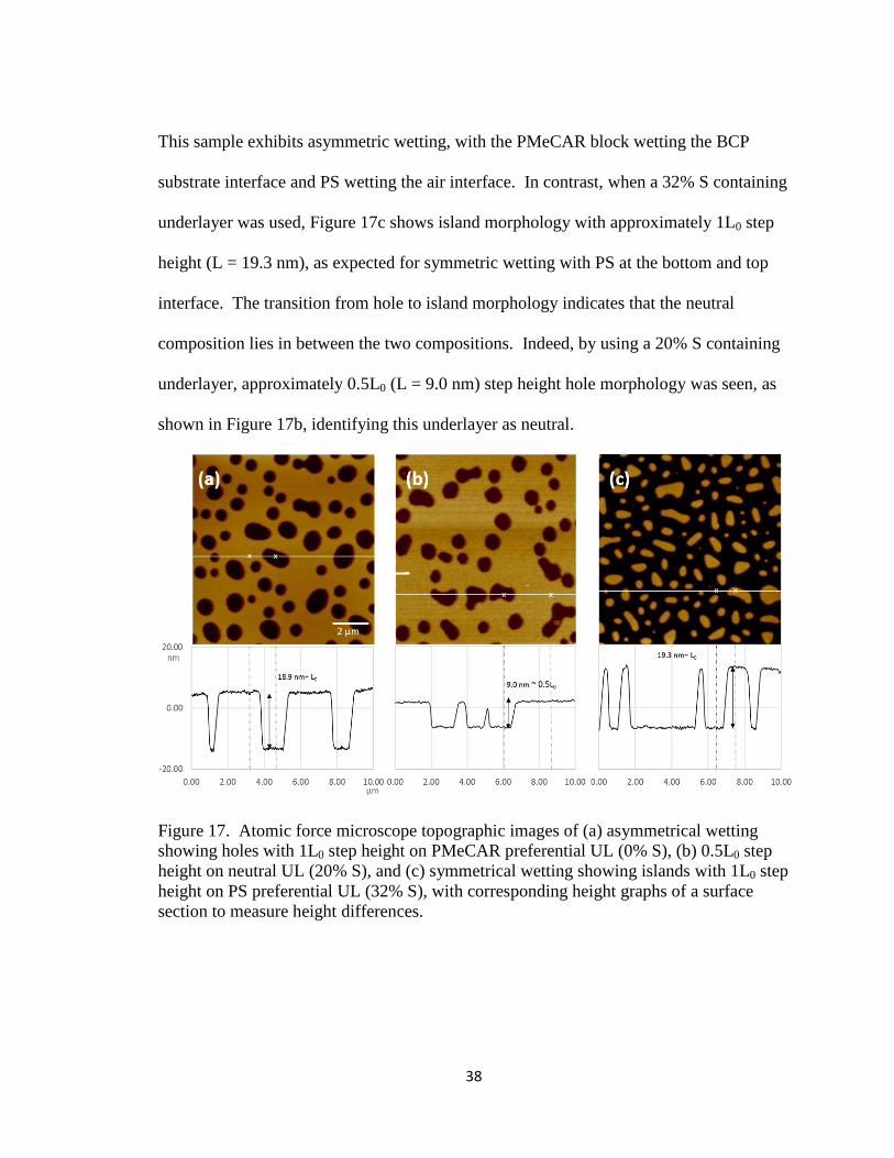
38
This sample exhibits asymmetric wetting, with the PMeCAR block wetting the BCP
substrate interface and PS wetting the air interface. In contrast, when a 32% S containing
underlayer was used, Figure 17c shows island morphology with approximately 1L0 step
height (L = 19.3 nm), as expected for symmetric wetting with PS at the bottom and top
interface. The transition from hole to island morphology indicates that the neutral
composition lies in between the two compositions. Indeed, by using a 20% S containing
underlayer, approximately 0.5L0 (L = 9.0 nm) step height hole morphology was seen, as
shown in Figure 17b, identifying this underlayer as neutral.
Figure 17. Atomic force microscope topographic images of (a) asymmetrical wetting
showing holes with 1L0 step height on PMeCAR preferential UL (0% S), (b) 0.5L0 step
height on neutral UL (20% S), and (c) symmetrical wetting showing islands with 1L0 step
height on PS preferential UL (32% S), with corresponding height graphs of a surface
section to measure height differences.
39
5.2 Air Interface Control
Following the successful identification of 20% S as the neutral underlayer,
formulations of PS-b-PMeCAR with different SAP compositions and concentrations
were prepared for orientation control at the air interface. In general, fluorinated groups
are surface active, and therefore have a lower surface energy than polystyrene [38]. By
using polymers containing fluorinated groups, it was postulated that these SAPs could
enable orientation control at the BCP-air interface through two key design parameters.
First, the SAP has a lower surface energy than either of the individual BCP components,
PS or PMeCAR in this case. Second, the SAP has a preferential interaction with the
more polar, higher surface energy block of the BCP. The combined design parameters in
the SAP should help in balancing the surface energies of the two BCP components at the
BCP-air interface by preferentially interacting with the polar component and bringing it
to the air interface. In this section, the results of the effects of the different SAP
compositions and concentrations on orientation are presented.
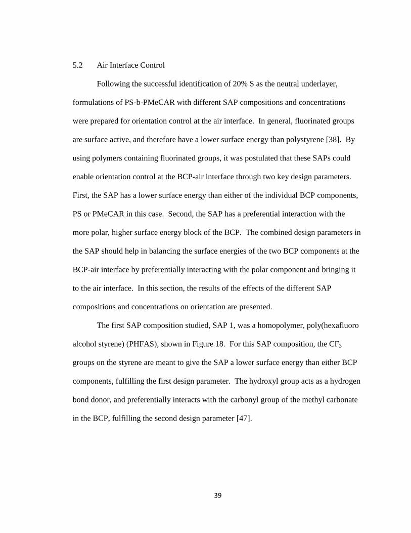
The first SAP composition studied, SAP 1, was a homopolymer, poly(hexafluoro
alcohol styrene) (PHFAS), shown in Figure 18. For this SAP composition, the CF3
groups on the styrene are meant to give the SAP a lower surface energy than either BCP
components, fulfilling the first design parameter. The hydroxyl group acts as a hydrogen
bond donor, and preferentially interacts with the carbonyl group of the methyl carbonate
in the BCP, fulfilling the second design parameter [47].
40
Figure 18. Structure of PHFAS (SAP 1).
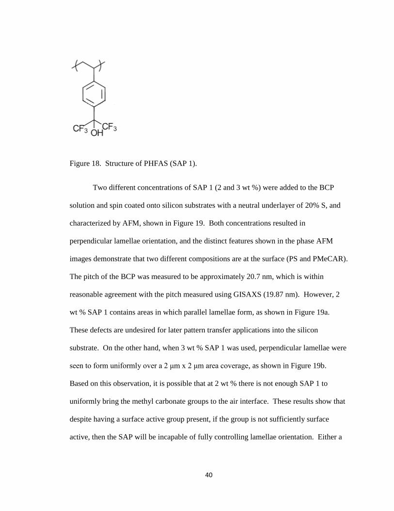
Two different concentrations of SAP 1 (2 and 3 wt %) were added to the BCP
solution and spin coated onto silicon substrates with a neutral underlayer of 20% S, and
characterized by AFM, shown in Figure 19. Both concentrations resulted in
perpendicular lamellae orientation, and the distinct features shown in the phase AFM
images demonstrate that two different compositions are at the surface (PS and PMeCAR).
The pitch of the BCP was measured to be approximately 20.7 nm, which is within
reasonable agreement with the pitch measured using GISAXS (19.87 nm). However, 2
wt % SAP 1 contains areas in which parallel lamellae form, as shown in Figure 19a.
These defects are undesired for later pattern transfer applications into the silicon
substrate. On the other hand, when 3 wt % SAP 1 was used, perpendicular lamellae were
seen to form uniformly over a 2 μm x 2 μm area coverage, as shown in Figure 19b.
Based on this observation, it is possible that at 2 wt % there is not enough SAP 1 to
uniformly bring the methyl carbonate groups to the air interface. These results show that
despite having a surface active group present, if the group is not sufficiently surface
active, then the SAP will be incapable of fully controlling lamellae orientation. Either a
41
higher concentration of SAP 1 is needed, as shown by the need to use 3 wt %, or a more
surface active group is necessary for proper orientation control.
Figure 19. Atomic force microscope phase images of PS-b-PMeCAR + SAP 1 on a
modified neutral substrate with (a) 2 wt % and (b) 3 wt % SAP 1. Scale bar: 400 nm.
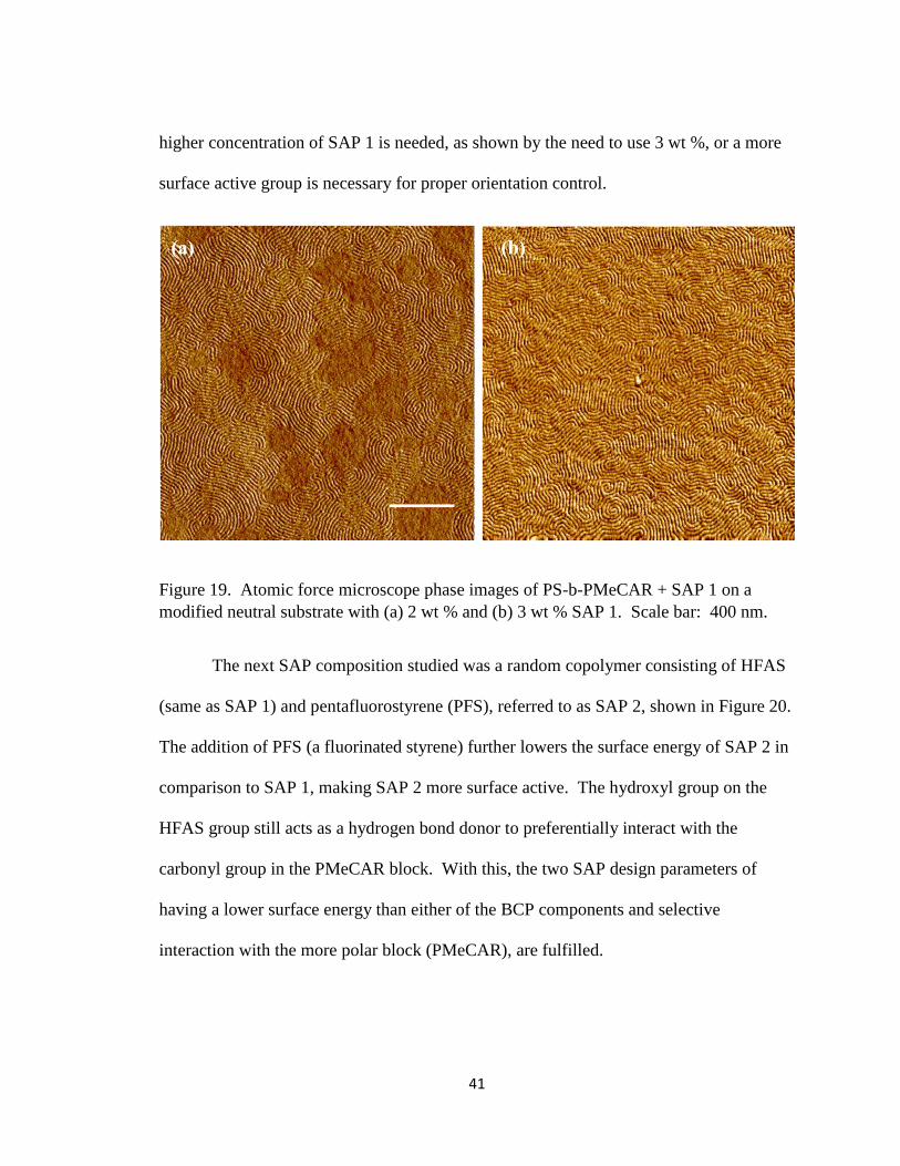
The next SAP composition studied was a random copolymer consisting of HFAS
(same as SAP 1) and pentafluorostyrene (PFS), referred to as SAP 2, shown in Figure 20.
The addition of PFS (a fluorinated styrene) further lowers the surface energy of SAP 2 in
comparison to SAP 1, making SAP 2 more surface active. The hydroxyl group on the
HFAS group still acts as a hydrogen bond donor to preferentially interact with the
carbonyl group in the PMeCAR block. With this, the two SAP design parameters of
having a lower surface energy than either of the BCP components and selective
interaction with the more polar block (PMeCAR), are fulfilled.
42
Figure 20. Structure of SAP 2, PHFAS-r-PPFS.
Because SAP 2 is a random copolymer containing two different components, a
study varying the mole ratio of PFS to HFAS was done to better understand the effect of
surface activity. The two different ratios studied were 40:60 (SAP 2-40) and 80:20 (SAP
2-80). By increasing the amount of PFS, the surface energy of the SAP is further
reduced, so SAP 2-80 is more surface active than either SAP 1 or SAP 2-40.
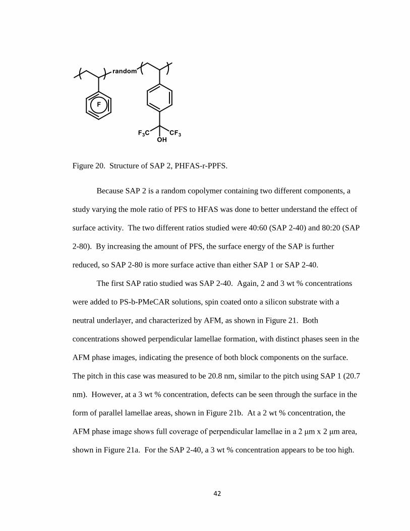
The first SAP ratio studied was SAP 2-40. Again, 2 and 3 wt % concentrations
were added to PS-b-PMeCAR solutions, spin coated onto a silicon substrate with a
neutral underlayer, and characterized by AFM, as shown in Figure 21. Both
concentrations showed perpendicular lamellae formation, with distinct phases seen in the
AFM phase images, indicating the presence of both block components on the surface.
The pitch in this case was measured to be 20.8 nm, similar to the pitch using SAP 1 (20.7
nm). However, at a 3 wt % concentration, defects can be seen through the surface in the
form of parallel lamellae areas, shown in Figure 21b. At a 2 wt % concentration, the
AFM phase image shows full coverage of perpendicular lamellae in a 2 μm x 2 μm area,
shown in Figure 21a. For the SAP 2-40, a 3 wt % concentration appears to be too high.
43
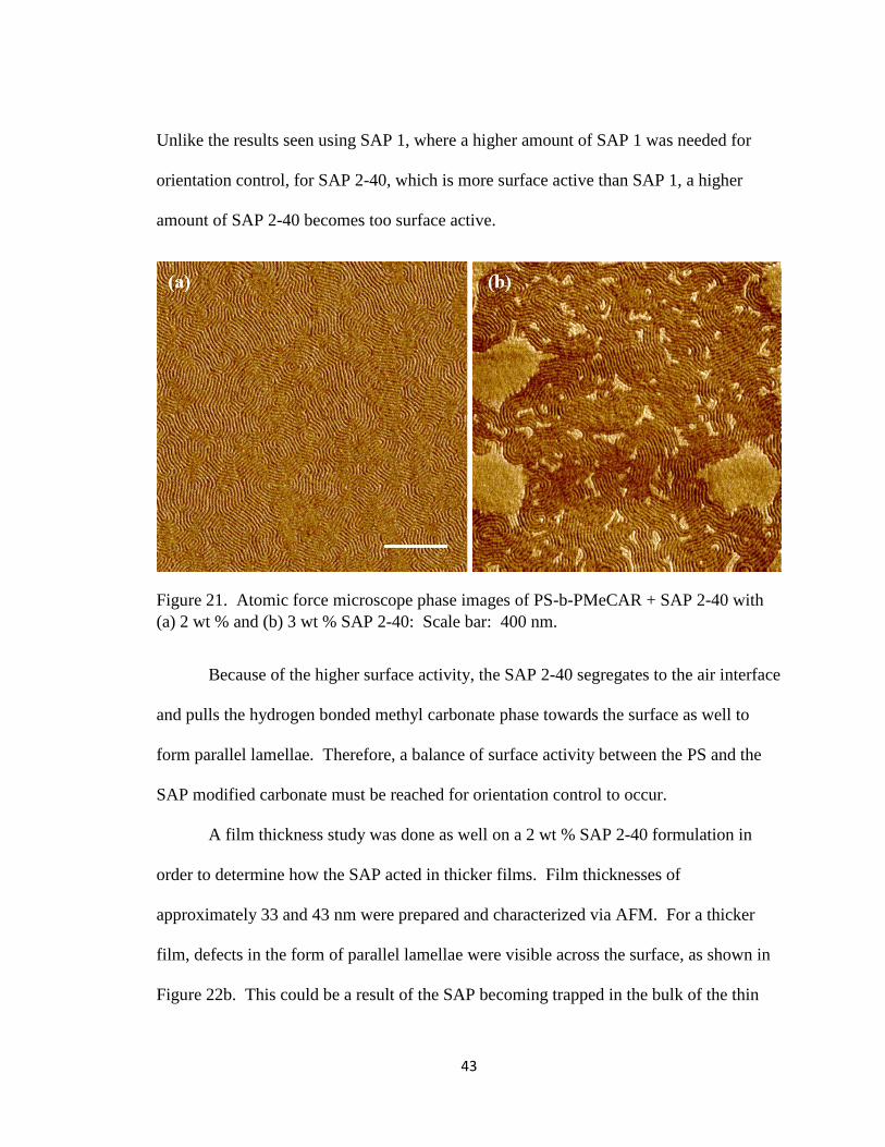
Unlike the results seen using SAP 1, where a higher amount of SAP 1 was needed for
orientation control, for SAP 2-40, which is more surface active than SAP 1, a higher
amount of SAP 2-40 becomes too surface active.
Figure 21. Atomic force microscope phase images of PS-b-PMeCAR + SAP 2-40 with
(a) 2 wt % and (b) 3 wt % SAP 2-40: Scale bar: 400 nm.
Because of the higher surface activity, the SAP 2-40 segregates to the air interface
and pulls the hydrogen bonded methyl carbonate phase towards the surface as well to
form parallel lamellae. Therefore, a balance of surface activity between the PS and the
SAP modified carbonate must be reached for orientation control to occur.
A film thickness study was done as well on a 2 wt % SAP 2-40 formulation in
order to determine how the SAP acted in thicker films. Film thicknesses of
approximately 33 and 43 nm were prepared and characterized via AFM. For a thicker
film, defects in the form of parallel lamellae were visible across the surface, as shown in
Figure 22b. This could be a result of the SAP becoming trapped in the bulk of the thin
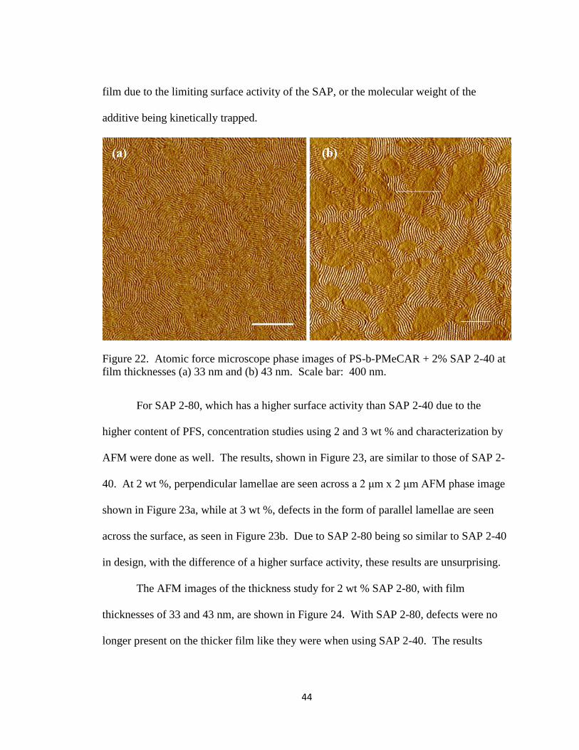
44
film due to the limiting surface activity of the SAP, or the molecular weight of the
additive being kinetically trapped.
Figure 22. Atomic force microscope phase images of PS-b-PMeCAR + 2% SAP 2-40 at
film thicknesses (a) 33 nm and (b) 43 nm. Scale bar: 400 nm.
For SAP 2-80, which has a higher surface activity than SAP 2-40 due to the
higher content of PFS, concentration studies using 2 and 3 wt % and characterization by
AFM were done as well. The results, shown in Figure 23, are similar to those of SAP 2-
40. At 2 wt %, perpendicular lamellae are seen across a 2 μm x 2 μm AFM phase image
shown in Figure 23a, while at 3 wt %, defects in the form of parallel lamellae are seen
across the surface, as seen in Figure 23b. Due to SAP 2-80 being so similar to SAP 2-40
in design, with the difference of a higher surface activity, these results are unsurprising.
The AFM images of the thickness study for 2 wt % SAP 2-80, with film
thicknesses of 33 and 43 nm, are shown in Figure 24. With SAP 2-80, defects were no
longer present on the thicker film like they were when using SAP 2-40. The results
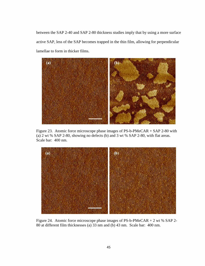
45
between the SAP 2-40 and SAP 2-80 thickness studies imply that by using a more surface
active SAP, less of the SAP becomes trapped in the thin film, allowing for perpendicular
lamellae to form in thicker films.
Figure 23. Atomic force microscope phase images of PS-b-PMeCAR + SAP 2-80 with
(a) 2 wt % SAP 2-80, showing no defects (b) and 3 wt % SAP 2-80, with flat areas.
Scale bar: 400 nm.
Figure 24. Atomic force microscope phase images of PS-b-PMeCAR + 2 wt % SAP 2-
80 at different film thicknesses (a) 33 nm and (b) 43 nm. Scale bar: 400 nm.
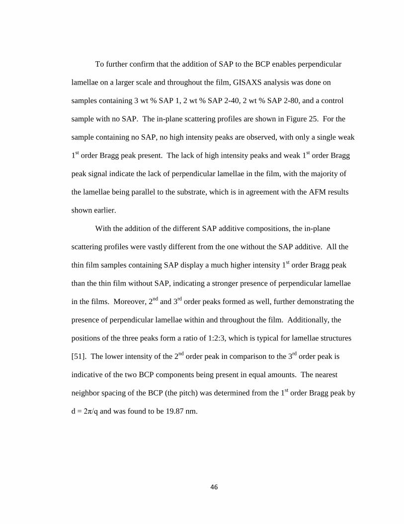
46
To further confirm that the addition of SAP to the BCP enables perpendicular
lamellae on a larger scale and throughout the film, GISAXS analysis was done on
samples containing 3 wt % SAP 1, 2 wt % SAP 2-40, 2 wt % SAP 2-80, and a control
sample with no SAP. The in-plane scattering profiles are shown in Figure 25. For the
sample containing no SAP, no high intensity peaks are observed, with only a single weak
1st order Bragg peak present. The lack of high intensity peaks and weak 1
st order Bragg
peak signal indicate the lack of perpendicular lamellae in the film, with the majority of
the lamellae being parallel to the substrate, which is in agreement with the AFM results
shown earlier.
With the addition of the different SAP additive compositions, the in-plane
scattering profiles were vastly different from the one without the SAP additive. All the
thin film samples containing SAP display a much higher intensity 1st order Bragg peak
than the thin film without SAP, indicating a stronger presence of perpendicular lamellae
in the films. Moreover, 2nd
and 3rd
order peaks formed as well, further demonstrating the
presence of perpendicular lamellae within and throughout the film. Additionally, the
positions of the three peaks form a ratio of 1:2:3, which is typical for lamellae structures
[51]. The lower intensity of the 2nd
order peak in comparison to the 3rd
order peak is
indicative of the two BCP components being present in equal amounts. The nearest
neighbor spacing of the BCP (the pitch) was determined from the 1st order Bragg peak by
d = 2π/q and was found to be 19.87 nm.
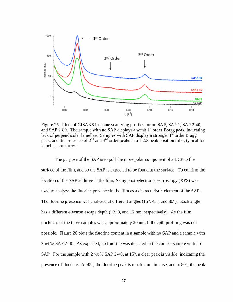
47
Figure 25. Plots of GISAXS in-plane scattering profiles for no SAP, SAP 1, SAP 2-40,
and SAP 2-80. The sample with no SAP displays a weak 1st order Bragg peak, indicating
lack of perpendicular lamellae. Samples with SAP display a stronger 1st order Bragg
peak, and the presence of 2nd
and 3rd
order peaks in a 1:2:3 peak position ratio, typical for
lamellae structures.
The purpose of the SAP is to pull the more polar component of a BCP to the
surface of the film, and so the SAP is expected to be found at the surface. To confirm the
location of the SAP additive in the film, X-ray photoelectron spectroscopy (XPS) was
used to analyze the fluorine presence in the film as a characteristic element of the SAP.
The fluorine presence was analyzed at different angles (15°, 45°, and 80°). Each angle
has a different electron escape depth (~3, 8, and 12 nm, respectively). As the film
thickness of the three samples was approximately 30 nm, full depth profiling was not
possible. Figure 26 plots the fluorine content in a sample with no SAP and a sample with
2 wt % SAP 2-40. As expected, no fluorine was detected in the control sample with no
SAP. For the sample with 2 wt % SAP 2-40, at 15°, a clear peak is visible, indicating the
presence of fluorine. At 45°, the fluorine peak is much more intense, and at 80°, the peak
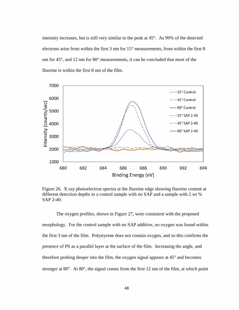
48
intensity increases, but is still very similar to the peak at 45°. As 99% of the detected
electrons arise from within the first 3 nm for 15° measurements, from within the first 8
nm for 45°, and 12 nm for 80° measurements, it can be concluded that most of the
fluorine is within the first 8 nm of the film.
Figure 26. X-ray photoelectron spectra at the fluorine edge showing fluorine content at
different detection depths in a control sample with no SAP and a sample with 2 wt %
SAP 2-40.
The oxygen profiles, shown in Figure 27, were consistent with the proposed
morphology. For the control sample with no SAP additive, no oxygen was found within
the first 3 nm of the film. Polystyrene does not contain oxygen, and so this confirms the
presence of PS as a parallel layer at the surface of the film. Increasing the angle, and
therefore probing deeper into the film, the oxygen signal appears at 45° and becomes
stronger at 80°. At 80°, the signal comes from the first 12 nm of the film, at which point
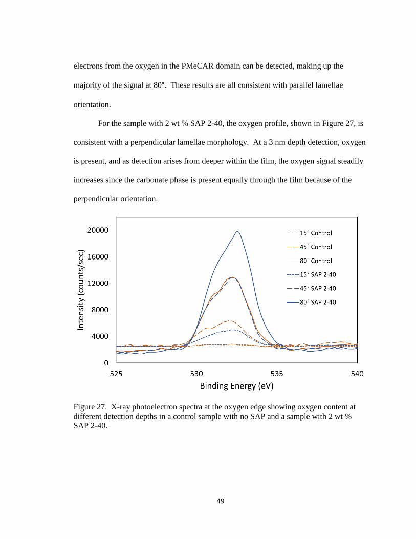
49
electrons from the oxygen in the PMeCAR domain can be detected, making up the
majority of the signal at 80°. These results are all consistent with parallel lamellae
orientation.
For the sample with 2 wt % SAP 2-40, the oxygen profile, shown in Figure 27, is
consistent with a perpendicular lamellae morphology. At a 3 nm depth detection, oxygen
is present, and as detection arises from deeper within the film, the oxygen signal steadily
increases since the carbonate phase is present equally through the film because of the
perpendicular orientation.
Figure 27. X-ray photoelectron spectra at the oxygen edge showing oxygen content at
different detection depths in a control sample with no SAP and a sample with 2 wt %
SAP 2-40.
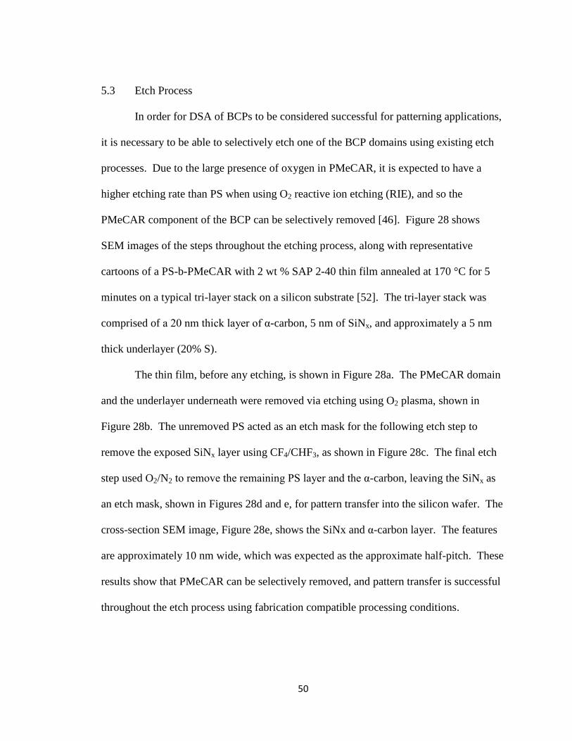
50
5.3 Etch Process
In order for DSA of BCPs to be considered successful for patterning applications,
it is necessary to be able to selectively etch one of the BCP domains using existing etch
processes. Due to the large presence of oxygen in PMeCAR, it is expected to have a
higher etching rate than PS when using O2 reactive ion etching (RIE), and so the
PMeCAR component of the BCP can be selectively removed [46]. Figure 28 shows
SEM images of the steps throughout the etching process, along with representative
cartoons of a PS-b-PMeCAR with 2 wt % SAP 2-40 thin film annealed at 170 °C for 5
minutes on a typical tri-layer stack on a silicon substrate [52]. The tri-layer stack was
comprised of a 20 nm thick layer of α-carbon, 5 nm of SiNx, and approximately a 5 nm
thick underlayer (20% S).
The thin film, before any etching, is shown in Figure 28a. The PMeCAR domain
and the underlayer underneath were removed via etching using O2 plasma, shown in
Figure 28b. The unremoved PS acted as an etch mask for the following etch step to
remove the exposed SiNx layer using CF4/CHF3, as shown in Figure 28c. The final etch
step used O2/N2 to remove the remaining PS layer and the α-carbon, leaving the SiNx as
an etch mask, shown in Figures 28d and e, for pattern transfer into the silicon wafer. The
cross-section SEM image, Figure 28e, shows the SiNx and α-carbon layer. The features
are approximately 10 nm wide, which was expected as the approximate half-pitch. These
results show that PMeCAR can be selectively removed, and pattern transfer is successful
throughout the etch process using fabrication compatible processing conditions.
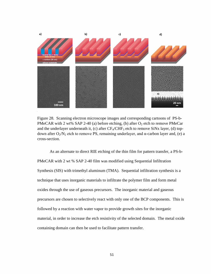
51
Fi
Figure 28. Scanning electron microscope images and corresponding cartoons of PS-b-
PMeCAR with 2 wt% SAP 2-40 (a) before etching, (b) after O2 etch to remove PMeCar
and the underlayer underneath it, (c) after CF4/CHF3 etch to remove SiNx layer, (d) top-
down after O2/N2 etch to remove PS, remaining underlayer, and α-carbon layer and, (e) a
cross-section.
As an alternate to direct RIE etching of the thin film for pattern transfer, a PS-b-
PMeCAR with 2 wt % SAP 2-40 film was modified using Sequential Infiltration
Synthesis (SIS) with trimethyl aluminum (TMA). Sequential infiltration synthesis is a
technique that uses inorganic materials to infiltrate the polymer film and form metal
oxides through the use of gaseous precursors. The inorganic material and gaseous
precursors are chosen to selectively react with only one of the BCP components. This is
followed by a reaction with water vapor to provide growth sites for the inorganic
material, in order to increase the etch resistivity of the selected domain. The metal oxide
containing domain can then be used to facilitate pattern transfer.
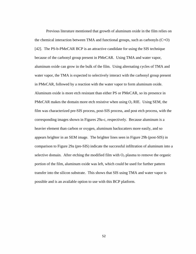
52
Previous literature mentioned that growth of aluminum oxide in the film relies on
the chemical interaction between TMA and functional groups, such as carbonyls (C=O)
[42]. The PS-b-PMeCAR BCP is an attractive candidate for using the SIS technique
because of the carbonyl group present in PMeCAR. Using TMA and water vapor,
aluminum oxide can grow in the bulk of the film. Using alternating cycles of TMA and
water vapor, the TMA is expected to selectively interact with the carbonyl group present
in PMeCAR, followed by a reaction with the water vapor to form aluminum oxide.
Aluminum oxide is more etch resistant than either PS or PMeCAR, so its presence in
PMeCAR makes the domain more etch resistive when using O2 RIE. Using SEM, the
film was characterized pre-SIS process, post-SIS process, and post etch process, with the
corresponding images shown in Figures 29a-c, respectively. Because aluminum is a
heavier element than carbon or oxygen, aluminum backscatters more easily, and so
appears brighter in an SEM image. The brighter lines seen in Figure 29b (post-SIS) in
comparison to Figure 29a (pre-SIS) indicate the successful infiltration of aluminum into a
selective domain. After etching the modified film with O2 plasma to remove the organic
portion of the film, aluminum oxide was left, which could be used for further pattern
transfer into the silicon substrate. This shows that SIS using TMA and water vapor is
possible and is an available option to use with this BCP platform.
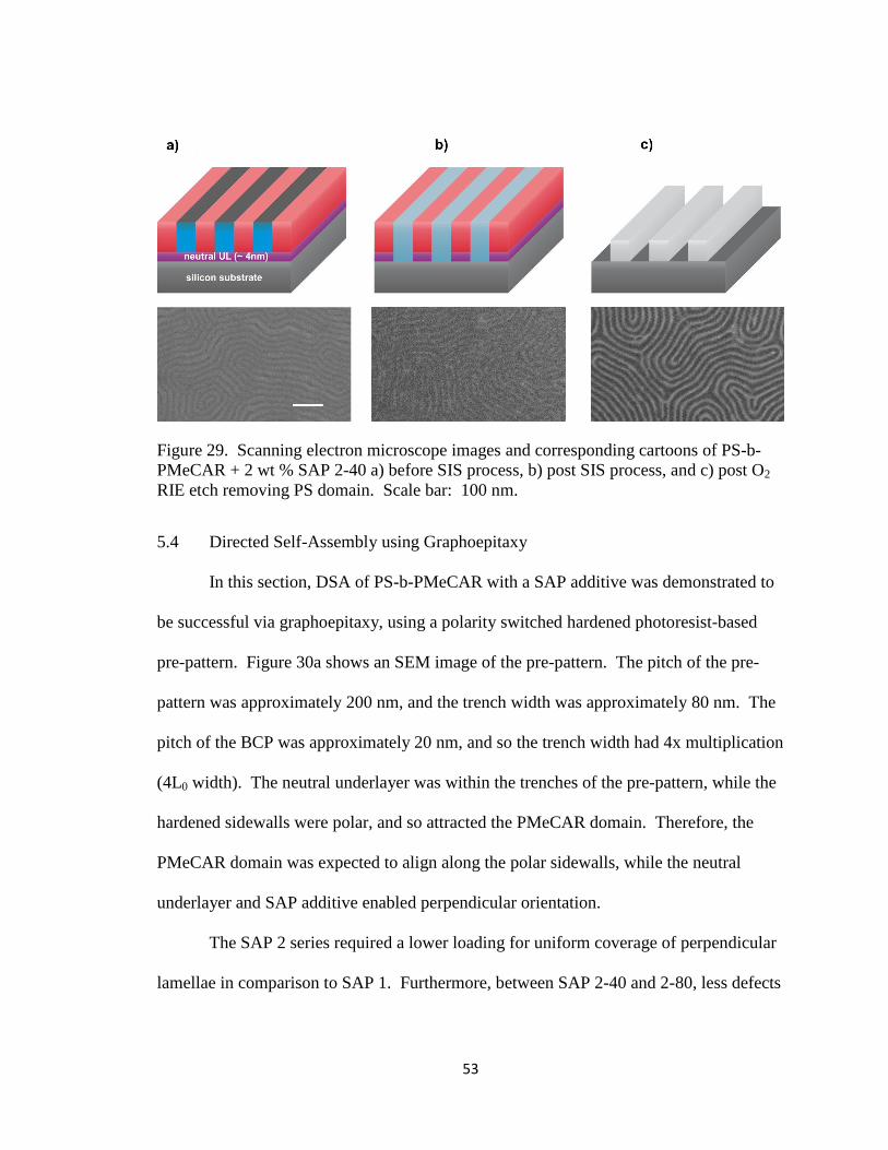
53
Figure 29. Scanning electron microscope images and corresponding cartoons of PS-b-
PMeCAR + 2 wt % SAP 2-40 a) before SIS process, b) post SIS process, and c) post O2
RIE etch removing PS domain. Scale bar: 100 nm.
5.4 Directed Self-Assembly using Graphoepitaxy
In this section, DSA of PS-b-PMeCAR with a SAP additive was demonstrated to
be successful via graphoepitaxy, using a polarity switched hardened photoresist-based
pre-pattern. Figure 30a shows an SEM image of the pre-pattern. The pitch of the pre-
pattern was approximately 200 nm, and the trench width was approximately 80 nm. The
pitch of the BCP was approximately 20 nm, and so the trench width had 4x multiplication
(4L0 width). The neutral underlayer was within the trenches of the pre-pattern, while the
hardened sidewalls were polar, and so attracted the PMeCAR domain. Therefore, the
PMeCAR domain was expected to align along the polar sidewalls, while the neutral
underlayer and SAP additive enabled perpendicular orientation.
The SAP 2 series required a lower loading for uniform coverage of perpendicular
lamellae in comparison to SAP 1. Furthermore, between SAP 2-40 and 2-80, less defects
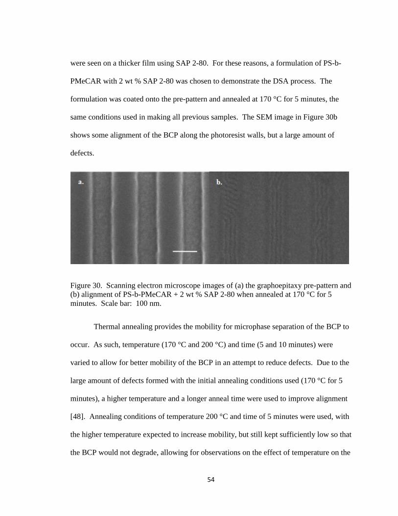
54
were seen on a thicker film using SAP 2-80. For these reasons, a formulation of PS-b-
PMeCAR with 2 wt % SAP 2-80 was chosen to demonstrate the DSA process. The
formulation was coated onto the pre-pattern and annealed at 170 °C for 5 minutes, the
same conditions used in making all previous samples. The SEM image in Figure 30b
shows some alignment of the BCP along the photoresist walls, but a large amount of
defects.
Figure 30. Scanning electron microscope images of (a) the graphoepitaxy pre-pattern and
(b) alignment of PS-b-PMeCAR + 2 wt % SAP 2-80 when annealed at 170 °C for 5
minutes. Scale bar: 100 nm.
Thermal annealing provides the mobility for microphase separation of the BCP to
occur. As such, temperature (170 °C and 200 °C) and time (5 and 10 minutes) were
varied to allow for better mobility of the BCP in an attempt to reduce defects. Due to the
large amount of defects formed with the initial annealing conditions used (170 °C for 5
minutes), a higher temperature and a longer anneal time were used to improve alignment
[48]. Annealing conditions of temperature 200 °C and time of 5 minutes were used, with
the higher temperature expected to increase mobility, but still kept sufficiently low so that
the BCP would not degrade, allowing for observations on the effect of temperature on the
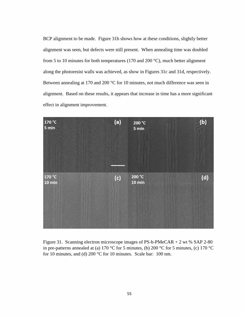
55
BCP alignment to be made. Figure 31b shows how at these conditions, slightly better
alignment was seen, but defects were still present. When annealing time was doubled
from 5 to 10 minutes for both temperatures (170 and 200 °C), much better alignment
along the photoresist walls was achieved, as show in Figures 31c and 31d, respectively.
Between annealing at 170 and 200 °C for 10 minutes, not much difference was seen in
alignment. Based on these results, it appears that increase in time has a more significant
effect in alignment improvement.
Figure 31. Scanning electron microscope images of PS-b-PMeCAR + 2 wt % SAP 2-80
in pre-patterns annealed at (a) 170 °C for 5 minutes, (b) 200 °C for 5 minutes, (c) 170 °C
for 10 minutes, and (d) 200 °C for 10 minutes. Scale bar: 100 nm.
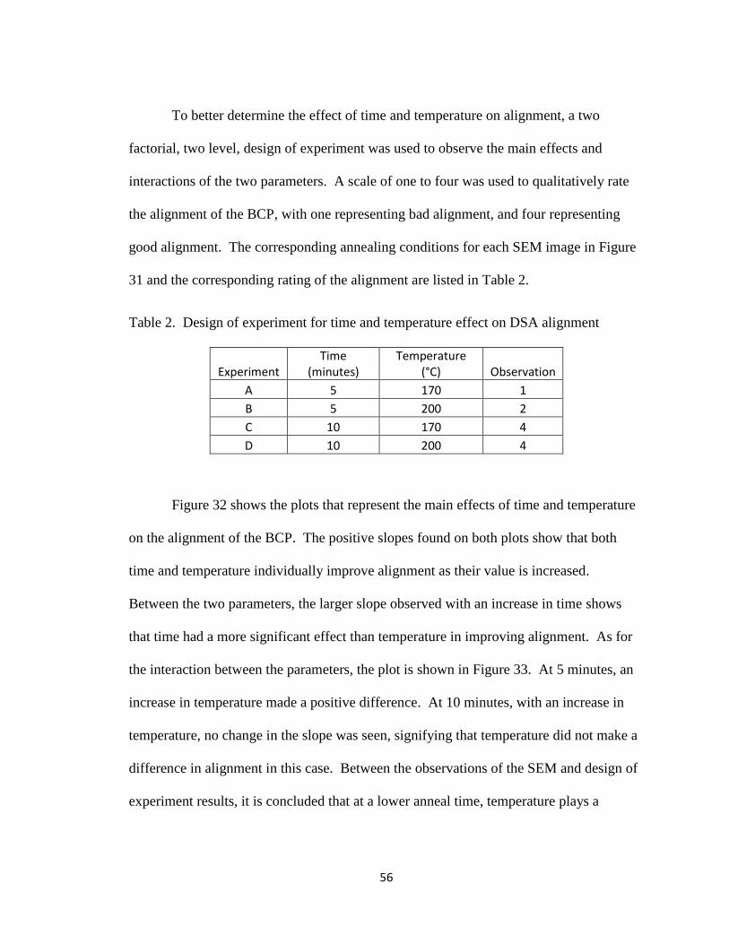
56
To better determine the effect of time and temperature on alignment, a two
factorial, two level, design of experiment was used to observe the main effects and
interactions of the two parameters. A scale of one to four was used to qualitatively rate
the alignment of the BCP, with one representing bad alignment, and four representing
good alignment. The corresponding annealing conditions for each SEM image in Figure
31 and the corresponding rating of the alignment are listed in Table 2.
Table 2. Design of experiment for time and temperature effect on DSA alignment
Experiment Time
(minutes) Temperature
(°C) Observation
A 5 170 1
B 5 200 2
C 10 170 4
D 10 200 4
Figure 32 shows the plots that represent the main effects of time and temperature
on the alignment of the BCP. The positive slopes found on both plots show that both
time and temperature individually improve alignment as their value is increased.
Between the two parameters, the larger slope observed with an increase in time shows
that time had a more significant effect than temperature in improving alignment. As for
the interaction between the parameters, the plot is shown in Figure 33. At 5 minutes, an
increase in temperature made a positive difference. At 10 minutes, with an increase in
temperature, no change in the slope was seen, signifying that temperature did not make a
difference in alignment in this case. Between the observations of the SEM and design of
experiment results, it is concluded that at a lower anneal time, temperature plays a
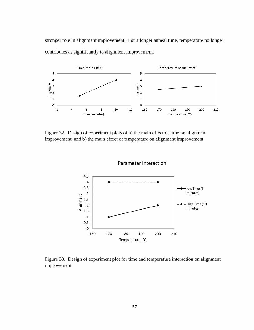
57
stronger role in alignment improvement. For a longer anneal time, temperature no longer
contributes as significantly to alignment improvement.
Figure 32. Design of experiment plots of a) the main effect of time on alignment
improvement, and b) the main effect of temperature on alignment improvement.
Figure 33. Design of experiment plot for time and temperature interaction on alignment
improvement.
58
CHAPTER SIX
CONCLUSIONS
A study of high-χ PS-b-PMeCAR BCP thin films with SAP additives for sub-20
nm pitch lamellae orientation control was reported. This method enables a fabrication
process comparable to the current PS-b-PMMA process (i.e., spin coated from
fabrication-friendly solvent PGMEA, thermally annealed, and no additional processing
steps needed) for a BCP with sub-20 nm features that PS-b-PMMA does not offer. Using
the method previously reported by Kim et al. to identify a neutral underlayer, PS-b-
PMeCAR on PS-r-PMMA with 20% S formed 0.5L0 step height features [27]. With the
addition of the SAP additive to the BCP formulation, successful orientation control at the
BCP-air interface was demonstrated, as verified by AFM, GISAXS, and XPS.
Furthermore, low concentrations of 2-3 wt % SAP were sufficient for obtaining uniform
perpendicular lamellae in this formulation based method, as opposed to previous reported
values of 10-20 wt %.
The balance between the surface activity and concentration of the SAP was
demonstrated to be significant in obtaining defect-free perpendicular lamellae. The SAP
1, which has a lower surface activity than either of the SAP 2 series compositions,
required a higher concentration for uniform coverage. On the other hand, the more
surface active SAP 2 series required a lower concentration for uniform coverage, as
higher concentrations began forming parallel lamellae at the surface. Thickness studies
on the SAP 2 series showed that for thicker films, a more surface active SAP is preferable
59
for perpendicular lamellae to form, since the less surface active SAP (SAP 2-40) showed
parallel lamellae formation in the thicker film.
Successful removal of PMeCAR from the pattern formed from a BCP with 2 wt
% SAP 2-40 formulation was demonstrated through the use of O2 RIE. Additionally,
implementation of SIS to selectively incorporate aluminum oxide into the PMeCAR
domain to decrease the etch rate in order to remove the PS domain through O2 RIE was
also successfully shown. Both methods gave similar results, as seen by SEM,
demonstrating the potential use of this platform for pattern transfer applications.
Graphoepitaxy with 4X pitch density was successfully done using a BCP with 2
wt % SAP 2-80 formulation. The previous annealing conditions used (170 °C, 5
minutes) showed defects when viewed with SEM, and so annealing temperature and time
were modified to reduce defect formation. Design of experiment and SEM results
showed higher temperatures have a positive effect on alignment at lower annealing times,
while at longer annealing times, temperature no longer appeared to have much of an
effect.
Overall, it was demonstrated that using a SAP based additive approach is
promising for control orientation of high-χ BCPs, and is compatible with existing etch
processes and graphoepitaxy schemes. Future work includes applying the SAP additives
on other BCP platforms and morphologies to enable sub-20 nm pitch features for
patterning work beyond lamellae morphology. Further optimization of the conditions for
DSA alignment, beyond the demonstration of its compatibility shown here, would also be
necessary for its successful use in patterning work.
60
REFERENCES
1. R. A. Robison, “Moore’s Law: Predictor and Driver of the Silicon Era,” World
Neurosurg., 78, 399–403 (2012).
2. Intel (2015). Moore’s Law 40th Anniversary [Online]. Available at
http://www.intel.com/pressroom/kits/events/moores_law_40th. (accessed: 04-Sep-
2015). WWW Article.
3. D. of E. and C. E. of G. T. University (2015). Photolithography [Online].
Available at http://www.ece.gatech.edu/research/labs/vc/theory/photolith.html.
(accessed: 10-Sep-2015). WWW Article.
4. J. I. Martı́n, J. Nogués, K. Liu, J. L. Vicent, and I. K. Schuller, “Ordered magnetic
nanostructures: fabrication and properties,” J. Magn. Magn. Mater., 256, 449–
501 (2003).
5. M. A. Morris, “Directed self-assembly of block copolymers for nanocircuitry
fabrication,” Microelectron. Eng., 132, 207–217 (2015).
6. C. M. Bates, M. J. Maher, D. W. Janes, C. J. Ellison, and C. G. Willson, “Block
copolymer lithography,” Macromolecules, 47, 2–12 (2014).
7. T. P. Lodge, “Block Copolymers : Past Successes and Future Challenges,”
Macrolmol. Chem. Phys., 204, 265–273 (2003).
8. C. T. Black, R. Ruiz, G. Breyta, J. Cheng, M. Coulborn, K. Guarini, H. Kim, and
Y. Zhang, “Polymer self-assembly in semiconductor microelectronics,” IBM J.
Res. Dev, 51, 605–633 (2007).
9. K. E. Sohn, “Surface Effects on the Structure of Block Copolymer and
Homopolymer Thin Films,” University of California, Santa Barbara (2008).
10. H. Kim, S.-M. Park, and W. D. Hinsberg, “Block Copolymer Based
Nanostructures : Materials , Processes , and Applications to Electronics,” Chem.
Rev., 110, 146–177 (2010).
11. Y. Mai, F. Zhng, and X. Feng, “Polymer-directed synthesis of metal oxide-
containing nanomaterials for electrochemical energy storage,” Nanoscale, 6, 106–
121 (2014).
12. D. Walton, G. Kellogg, and A. Mayes, “A free energy model for confined diblock
copolymers,” Macromolecules, 27, 6225–6228 (1994).
13. C. M. Bates, T. Seshimo, M. J. Maher, W. J. Durand, J. D. Cushen, L. M. Dean, G.
Blachut, C. J. Ellison, and C. G. Willson, “Polarity-switching top coats enable
orientation of sub-10-nm block copolymer domains,” Science., 338, 775–779
(2012).
61
14. H. Yoshida, H. S. Suh, a Ramirez-Hernandez, J. I. Lee, K. Aida, L. Wan, Y.
Ishida, Y. Tada, R. Ruiz, J. de Pablo, and P. F. Nealey, “Topcoat Approaches for
Directed Self-Assembly of Strongly Segregating Block Copolymer Thin Films,” J.
Photopolym. Sci. Technol., 26, 55–58 (2013).
15. S. Kim, P. F. Nealey, and F. S. Bates, “Decoupling bulk thermodynamics and
wetting characteristics of block copolymer thin films,” ACS Macro Lett., 1, 11–14
(2012).
16. A. Vora, IBM Research- Almaden, private communication (November 2015).
17. S. J. Jeong, J. Y. Kim, B. H. Kim, H. S. Moon, and S. O. Kim, “Directed self-
assembly of block copolymers for next generation nanolithography,” Mater.
Today, 16, 468–476 (2013).
18. S. O. Kim, H. H. Solak, M. P. Stoykovich, N. J. Ferrier, J. J. De Pablo, and P. F.
Nealey, “Epitaxial self-assembly of block copolymers on lithographically defined
nanopatterned substrates.,” Nature, 424, 411–4 (2003).
19. R. A. Segalman, H. Yokoyama, and E. J. Kramer, “Graphoepitaxy of spherical
domain block copolymer films,” Adv. Mater., 13, 1152–1155 (2001).
20. G. S. Doerk, J. Y. Cheng, G. Singh, C. T. Rettner, J. W. Pitera, S. Balakrishnan, N.
Arellano, and D. P. Sanders, “Enabling complex nanoscale pattern customization
using directed self-assembly,” Nat. Commun., 5, 1–8 (2014).
21. H. Tsai, J. W. Pitera, H. Miyazoe, S. Bangsaruntip, S. U. Engelmann, C. Liu, J. Y.
Cheng, J. J. Bucchignano, D. P. Klaus, E. A. Joseph, D. P. Sanders, M. E. Colburn,
and M. A. Guillorn, “Two-Dimensional Pattern Formation Using Graphoepitaxy
of PS ‑ b ‑ PMMA Block Copolymers for Advanced FinFET Device and Circuit
Fabrication,” ACS Nano, 8, 5227–5232 (2014).
22. P. Mansky, P. Haikin, and E. L. Thomas, “Monolayer films of diblock copolymer
microdomains for nanolithographic applications,” J. Mater. Sci., 30, 1987–1992
(1995).
23. G. J. Kellogg, D. G. Walton, A. M. Mayes, P. Lambooy, T. P. Russell, P. D.
Gallagher, and S. K. Satija, “Observed Surface Energy Effects in Confined Diblock
Copolymers,” Phys. Rev. Lett., 76, 2503–2506 (1996).
24. P. Mansky, Y. Liu, E. Huang, T. P. Russell, and C. J. Hawker, “Controlling
polymer-surface interactions with random copolymer brushes,” Science, 275,
1458–1460 (1997).
25. P. Mansky, T. P. Russell, C. J. Hawker, M. Pitsikalis, and J. Mays, “Ordered
diblock copolymer films on random copolymer brushes,” Macromolecules, 30,
6810–6813 (1997).
26. R. D. Peters, X. M. Yang, T. K. Kim, B. H. Sohn, and P. F. Nealey, “Using Self-
62
Assembled Monolayers Exposed to X-rays To Control the Wetting Behavior of
Thin Films of Diblock Copolymers,” Langmuir, 16, 4625–4631 (2000).
27. S. Kim, C. M. Bates, A. Thio, J. D. Cushen, C. J. Ellison, C. G. Willson, and F. S.
Bates, “Consequences of surface neutralization in diblock copolymer thin films,”
ACS Nano, 7, 9905–9919 (2013).
28. P. Mansky, T. Russell, C. Hawker, J. Mays, D. Cook, and S. Satija, “Interfacial
Segregation in Disordered Block Copolymers: Effect of Tunable Surface
Potentials,” Phys. Rev. Lett., 79, 237–240 (1997).
29. J. Zhang, M. B. Clark, C. Wu, M. Li, P. Trefonas, and P. D. Hustad, “Orientation
Control in Thin Films of a High-χ Block Copolymer with a Surface Active
Embedded Neutral Layer.,” Nano Lett., 16, 728–35 (2016).
30. J. G. Son, K. W. Gotrik, and C. A. Ross, “High-aspect-ratio perpendicular
orientation of PS- B -PDMS thin films under solvent annealing,” ACS Macro
Lett., 1, 1279–1284 (2012).
31. S. H. Kim, M. J. Misner, T. Xu, M. Kimura, and T. P. Russell, “Highly oriented
and ordered arrays from block copolymers via solvent evaporation,” Adv. Mater.,
16, 226–231 (2004).
32. A. Vora, R. J. Wojtecki, K. Schmidt, A. Chunder, J. Y. Cheng, A. Nelson, and D.
P. Sanders, “Development of polycarbonate-containing block copolymers for thin
film self-assembly applications,” Polym. Chem., 7, 940–950 (2016).
33. E. Han, K. O. Stuen, M. Leolukman, C. C. Liu, P. F. Nealey, and P. Gopalan,
“Perpendicular orientation of domains in cylinder-forming block copolymer thick
films by controlled interfacial interactions,” Macromolecules, 42, 4896–4901
(2009).
34. J. N. L. Albert, W. S. Young, R. L. Lewis, T. D. Bogart, J. R. Smith, and T. H.
Epps, “Systematic study on the effect of solvent removal rate on the morphology of
solvent vapor annealed ABA triblock copolymer thin films,” ACS Nano, 6, 459–
466 (2012).
35. C. Sinturel, M. Morris, and M. Hillmyer, “Solvent Vapor Annealing of Block
Polymer Thin Films,” Macromolecules, 46, 5399–5415 (2013).
36. R. J. Albalak, M. S. Capel, and E. L. Thomas, “Solvent swelling of roll-cast
triblock copolymer films,” Polymer., 39, 1647–1656 (1998).
37. X. Zhang, K. D. Harris, N. L. Y. Wu, J. N. Murphy, and J. M. Buriak, “Fast
Assembly of Ordered Block Copolymer Nanostructures through Microwave
Annealing,” ACS Nano, 4, 7021–7029 (2010).
38. E. Huang, T. P. Russell, C. Harrison, P. M. Chaikin, R. A. Register, C. J. Hawker,
and J. Mays, “Using Surface Active Random Copolymers To Control the Domain
63
Orientation in Diblock Copolymer Thin Films,” Macromolecules, 31, 7641–7650
(1998).
39. I. Keen, A. Yu, H. Cheng, K. S. Jack, T. M. Nicholson, A. K. Whittaker, and I.
Blakey, “Article pubs.acs.org/Langmuir Control of the Orientation of Symmetric
Poly(styrene)-block- poly(D,L‑lactide) Block Copolymers Using Statistical
Copolymers of Dissimilar Composition,” Langmuir, 45, 15876–15888 (2012).
40. H. Li, W. Gu, L. Li, Y. Zhang, T. P. Russell, and E. B. Coughlin, “Synthesis of
semicrystalline/fluorinated side-chain crystalline block copolymers and their bulk
and thin film nanoordering,” Macromolecules, 46, 3737–3745 (2013).
41. D. K. Owens and R. C. Wendt, “Estimation of the surface free energy of
polymers,” J. Appl. Polym. Sci., 13, 1741–1747 (1969).
42. M. Biswas, J. A. Libera, S. B. Darling, and J. W. Elam, “Kinetics for the
Sequential Infiltration Synthesis of Alumina in Poly(methyl methacrylate): An
Infrared Spectroscopic Study,” J. Phys. Chem. C, 119, 14585–14592 (2015).
43. R. A. Farrell, N. Petkov, M. T. Shaw, V. Djara, J. D. Holmes, and M. A. Morris,
“Monitoring PMMA Elimination by Reactive Ion Etching from a Lamellar PS-b-
PMMA Thin Film by ex Situ TEM Methods,” Macromolecules, 43, 8651–8655
(2010).
44. J. W. Elam, M. Biswas, S. Darling, A. Yanguas-Gil, J. D. Emery, A. B. F.
Martinson, P. F. Nealey, T. Segal-Peretz, Q. Peng, J. Winterstein, J. A. Liddle, and
Y.-C. Tseng, “New Insights into Sequential Infiltration Synthesis,” ECS Trans.,
69, 147–157 (2015).
45. Y. C. Tseng, Q. Peng, L. E. Ocola, J. W. Elam, and S. B. Darling, “Enhanced
block copolymer lithography using sequential infiltration synthesis,” J. Phys.
Chem. C, 115, 17725–17729 (2011).
46. H. Gokan, S. Esho, and Y. Ohnishi, “Dry Etch Resistance of Organic Materials,”
J. Electrochem. Soc., 130, 143–146 (1983).
47. O. Coulembier, D. P. Sanders, A. Nelson, A. N. Hollenbeck, H. W. Horn, J. E.
Rice, M. Fujiwara, P. Dubois, and J. L. Hedrick, “Hydrogen-bonding catalysts
based on fluorinated alcohol derivatives for living polymerization,” Angew.
Chemie - Int. Ed., 48, 5170–5173 (2009).
48. A. M. Welander, H. Kang, K. O. Stuen, H. H. Solak, M. Müller, J. J. De Pablo,
and P. F. Nealey, “Rapid Directed Assembly of Block Copolymer Films at
Elevated Temperatures,” Macromolecules, 41, 2759–2761 (2008).
49. A. Hexemer, W. Bras, J. Glossinger, E. Schaible, E. Gann, R. Kirian, A.
MacDowell, M. Church, B. Rude, and H. Padmore, “A SAXS/WAXS/GISAXS
Beamline with Multilayer Monocromator,” J. Phys. Conf., 247, 012007 (2010).
64
50. J. Ilavsky and P. Jemian, “Irena: tool suite for modeling and analysis of small-
angle scattering,” J. Appl. Crystallogr., 42, 347–353 (2009).
51. P. Busch, D. Posselt, D.-M. Smilgies, M. Rauscher, and C. M. Papadakis, “Inner
Structure of Thin Films of Lamellar Poly(styrene-b-butadiene) Diblock
Copolymers As Revealed by Grazing-Incidence Small-Angle Scattering,”
Macromolecules, 40, 630–640 (2007).
52. M. Weimer, Y. Wang, C. J. Neef, J. Claypool, K. Edwards, and Z. Zhu,
“Materials for and performance of multilayer lithography schemes,” Procs. SPIE
Conf., 2007.