MIC2230 - Dual Synchronous 800 mA/800 mA Step-Down DC/DC ...
1dc2603abf
DEMO MANUAL DC2603A-B
DESCRIPTION
LTM4650AEY-1 Dual 25A or Single 50A
DC/DC μModule Regulator
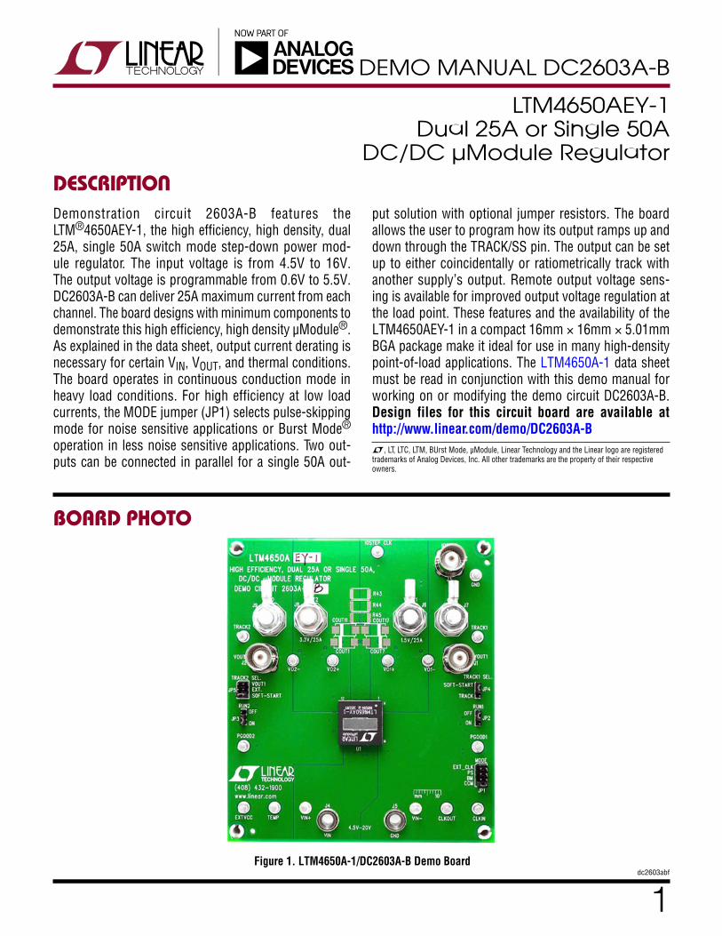
Demonstration circuit 2603A-B features the LTM®4650AEY-1, the high efficiency, high density, dual 25A, single 50A switch mode step-down power mod-ule regulator. The input voltage is from 4.5V to 16V. The output voltage is programmable from 0.6V to 5.5V. DC2603A-B can deliver 25A maximum current from each channel. The board designs with minimum components to demonstrate this high efficiency, high density µModule®. As explained in the data sheet, output current derating is necessary for certain VIN, VOUT, and thermal conditions. The board operates in continuous conduction mode in heavy load conditions. For high efficiency at low load currents, the MODE jumper (JP1) selects pulse-skipping mode for noise sensitive applications or Burst Mode® operation in less noise sensitive applications. Two out-puts can be connected in parallel for a single 50A out-
L, LT, LTC, LTM, BUrst Mode, µModule, Linear Technology and the Linear logo are registered trademarks of Analog Devices, Inc. All other trademarks are the property of their respective owners.
BOARD PHOTO
put solution with optional jumper resistors. The board allows the user to program how its output ramps up and down through the TRACK/SS pin. The output can be set up to either coincidentally or ratiometrically track with another supply’s output. Remote output voltage sens-ing is available for improved output voltage regulation at the load point. These features and the availability of the LTM4650AEY-1 in a compact 16mm × 16mm × 5.01mm BGA package make it ideal for use in many high-density point-of-load applications. The LTM4650A-1 data sheet must be read in conjunction with this demo manual for working on or modifying the demo circuit DC2603A-B. Design files for this circuit board are available at http://www.linear.com/demo/DC2603A-B
Figure 1. LTM4650A-1/DC2603A-B Demo Board
2dc2603abf
DEMO MANUAL DC2603A-B
QUICK START PROCEDUREDemonstration circuit DC2603A-B is easy to set up to evaluate the performance of the LTM4650AEY-1. Please refer to Figure 2 for proper measurement setup and follow the procedure below: 1. Place jumpers in the following positions for a typical
application:
JP1 JP2 JP3 JP4 JP5
MODE RUN1 RUN2 TRACK1 SEL TRACK2 SEL
CCM ON ON SOFT-START SOFT-START
2. With power off, connect the input power supply, load and meters as shown in Figure 2. Preset the load to 0A and VIN supply to 12V.
3. Turn on the power supply at the input. The output voltage in channel 1 should be 1.5V ± 1.0% (0.985V~1.015V) and the output voltage in channel 2 should be 3.3V±1.0% (3.267V~3.333V)
4. Once the proper output voltage is established, adjust the load within the operating range and observe the output voltage regulation, output voltage ripple, efficiency and other parameters. Output ripple can be measured at J1 and J2 with BNC cables.50Ω termination should be set on the oscilloscope or BNC cables.
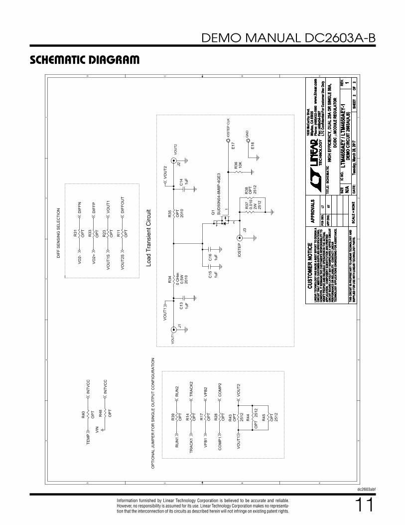
5. (Optional) For optional load transient test, apply an adjustable pulse signal between “IOSTEP CLK” and “GND” test point. Pulse amplitude (3V~3.5V) sets the load step current amplitude. The output transient current can be monitored at the BNC connector J3 (10mV/A). The pulse signal should have very small duty cycle (< 10%) to limit the thermal stress on the transient load circuit. Switch the jumper resistors R34 or R35 (on the backside of boards) to apply load transient on channel 1 or channel 2 correspondingly.
6. (Optional) LTM4650A-1 can be synchronized to an external clock signal. Place the JP1 jumper on EXT_CLK and apply a clock signal (0V~5V, square wave) on the CLKIN test point.
7. (Optional) The outputs of LTM4650A-1 can track another supply. The jumpers JP4 and JP5 allow choosing soft-start or output tracking. If tracking external voltage is selected, the corresponding test points, TRACK1 and TRACK2, need to be connected to a valid voltage signal.
8. (Optional) LTM4650A-1 can be configured for a 2-phase single output at up to 50A on DC2603A-B. Install 0Ω resis-tors on R14, R17, R28, R39, R43, R44, R45 and remove R7, R19. Output voltage is set by R25 based on equation:
VOUT =0.6V • 1+ 60.4k
R25⎛
⎝⎜
⎞
⎠⎟
PERFORMANCE SUMMARY Specifications are at TA = 25°C
PARAMETER CONDITIONS VALUE
Input Voltage Range 4.5V ~ 16V
Output Voltage VOUT1 VIN = 4.5~16V, IOUT1 = 0~25A, JP1: CCM 1.5V ± 1 % (1.485V ~ 1.515V)
Output Voltage VOUT2 VIN = 4.5~16V, IOUT1 = 0~25A, JP1: CCM 3.3V ± 1 % (3.267V ~ 3.333V)
Per- Channel Maximum Continuous Output Current
De-rating is Necessary for Certain VIN, VOUT and Thermal Conditions, see Data Sheet for Detail
25A
Default Operating Frequency 600kHz
Resistor Programmable Frequency Range 250kHz to 780kHz
External Clock Sync. Frequency Range 400kHz to 780kHz
Efficiency of Channel 1 VIN = 12V, VOUT = 1.5V, IOUT = 25A, fSW = 600 kHz 90.4%, See Figure 3
Efficiency of Channel 2 VIN = 12V, VOUT = 3.3V, IOUT = 25A, fSW = 600 kHz 94.2%, See Figure 4
Load Transient of Channel 1 VIN = 12V, VOUT = 1.5V, ISTEP = 12.5~18.75A < ±1.5% (45mVP-P), See Figure 5
Load Transient of Channel 2 VIN = 12V, VOUT = 3.3V, ISTEP = 12.5~18.75A < ±1.5% (99mVP-P), See Figure 6
3dc2603abf
DEMO MANUAL DC2603A-B
QUICK START PROCEDURE
LOAD1 (0~25A)
dc2603abf
1mΩ
VOUT1
VIN4.5V-16V
VOUT2
– + –+
LOAD2 (0~25A)1mΩ
+ –+–
+ –
+ –+–
Figure 2. Test Setup of DC2603A-B
4dc2603abf
DEMO MANUAL DC2603A-B
QUICK START PROCEDURE
Figure 3. Measured Efficiency on Channel 1 (VOUT1 = 1.5V, fSW = 600kHz, Channel2 Disabled)
Efficiency vs Load Current at VO = 3.3V, fSW = 600kHz
Efficiency vs Load Current at VO = 1.5V, fSW = 600kHz
Figure 4. Measured Efficiency on Channel 2 (VOUT2 = 3.3V, fSW = 600kHz, Channel1 Disabled)
5dc2603abf
DEMO MANUAL DC2603A-B
QUICK START PROCEDURE
Figure 5. Measured Channel 1 12.5A-18.75A Load Transient (VIN = 12V, VOUT1 = 1.5V)
Figure 6. Measured Channel 2 12.5A-18.75A Load Transient (VIN = 12V, VOUT2 = 3.3V)
3.3V Output (20MHz BW) [50mV/Div]
12.5A-18.75A Load Step
1.5V Output (20MHz BW) [20mV/Div]
12.5A-18.75A Load Step
6dc2603abf
DEMO MANUAL DC2603A-B
QUICK START PROCEDURE
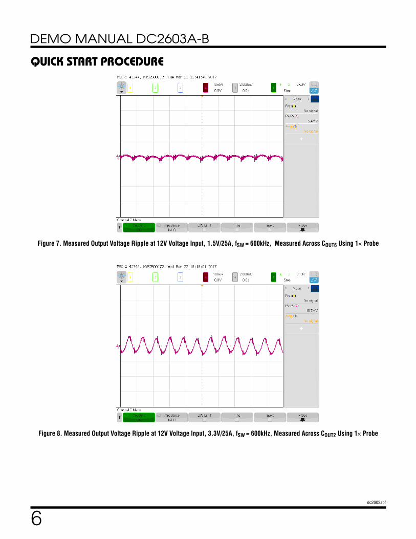
Figure 7. Measured Output Voltage Ripple at 12V Voltage Input, 1.5V/25A, fSW = 600kHz, Measured Across COUT6 Using 1× Probe
Figure 8. Measured Output Voltage Ripple at 12V Voltage Input, 3.3V/25A, fSW = 600kHz, Measured Across COUT2 Using 1× Probe
7dc2603abf
DEMO MANUAL DC2603A-B
QUICK START PROCEDURE
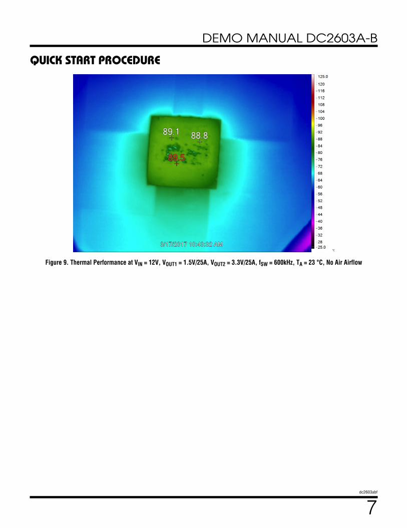
Figure 9. Thermal Performance at VIN = 12V, VOUT1 = 1.5V/25A, VOUT2 = 3.3V/25A, fSW = 600kHz, TA = 23 °C, No Air Airflow
8dc2603abf
DEMO MANUAL DC2603A-B
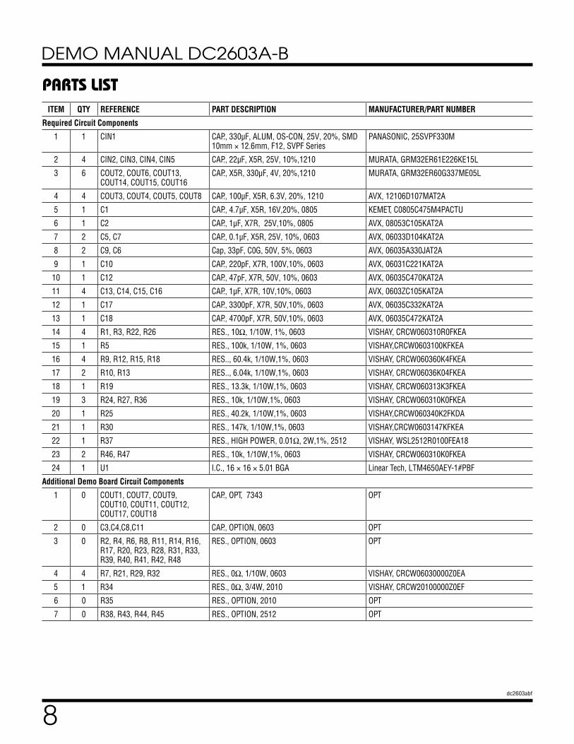
PARTS LISTITEM QTY REFERENCE PART DESCRIPTION MANUFACTURER/PART NUMBER
Required Circuit Components
1 1 CIN1 CAP., 330µF, ALUM, OS-CON, 25V, 20%, SMD 10mm × 12.6mm, F12, SVPF Series
PANASONIC, 25SVPF330M
2 4 CIN2, CIN3, CIN4, CIN5 CAP., 22µF, X5R, 25V, 10%,1210 MURATA, GRM32ER61E226KE15L
3 6 COUT2, COUT6, COUT13, COUT14, COUT15, COUT16
CAP., X5R, 330µF, 4V, 20%,1210 MURATA, GRM32ER60G337ME05L
4 4 COUT3, COUT4, COUT5, COUT8 CAP., 100µF, X5R, 6.3V, 20%, 1210 AVX, 12106D107MAT2A
5 1 C1 CAP., 4.7µF, X5R, 16V,20%, 0805 KEMET, C0805C475M4PACTU
6 1 C2 CAP., 1µF, X7R, 25V,10%, 0805 AVX, 08053C105KAT2A
7 2 C5, C7 CAP., 0.1µF, X5R, 25V, 10%, 0603 AVX, 06033D104KAT2A
8 2 C9, C6 Cap, 33pF, C0G, 50V, 5%, 0603 AVX, 06035A330JAT2A
9 1 C10 CAP., 220pF, X7R, 100V,10%, 0603 AVX, 06031C221KAT2A
10 1 C12 CAP., 47pF, X7R, 50V, 10%, 0603 AVX, 06035C470KAT2A
11 4 C13, C14, C15, C16 CAP., 1µF, X7R, 10V,10%, 0603 AVX, 0603ZC105KAT2A
12 1 C17 CAP., 3300pF, X7R, 50V,10%, 0603 AVX, 06035C332KAT2A
13 1 C18 CAP., 4700pF, X7R, 50V,10%, 0603 AVX, 06035C472KAT2A
14 4 R1, R3, R22, R26 RES., 10Ω, 1/10W, 1%, 0603 VISHAY, CRCW060310R0FKEA
15 1 R5 RES., 100k, 1/10W, 1%, 0603 VISHAY,CRCW0603100KFKEA
16 4 R9, R12, R15, R18 RES.., 60.4k, 1/10W,1%, 0603 VISHAY, CRCW060360K4FKEA
17 2 R10, R13 RES.., 6.04k, 1/10W,1%, 0603 VISHAY, CRCW06036K04FKEA
18 1 R19 RES., 13.3k, 1/10W,1%, 0603 VISHAY, CRCW060313K3FKEA
19 3 R24, R27, R36 RES., 10k, 1/10W,1%, 0603 VISHAY, CRCW060310K0FKEA
20 1 R25 RES., 40.2k, 1/10W,1%, 0603 VISHAY,CRCW060340K2FKDA
21 1 R30 RES., 147k, 1/10W,1%, 0603 VISHAY,CRCW0603147KFKEA
22 1 R37 RES., HIGH POWER, 0.01Ω, 2W,1%, 2512 VISHAY, WSL2512R0100FEA18
23 2 R46, R47 RES., 10k, 1/10W,1%, 0603 VISHAY, CRCW060310K0FKEA
24 1 U1 I.C., 16 × 16 × 5.01 BGA Linear Tech, LTM4650AEY-1#PBF
Additional Demo Board Circuit Components
1 0 COUT1, COUT7, COUT9, COUT10, COUT11, COUT12, COUT17, COUT18
CAP., OPT, 7343 OPT
2 0 C3,C4,C8,C11 CAP., OPTION, 0603 OPT
3 0 R2, R4, R6, R8, R11, R14, R16, R17, R20, R23, R28, R31, R33, R39, R40, R41, R42, R48
RES., OPTION, 0603 OPT
4 4 R7, R21, R29, R32 RES., 0Ω, 1/10W, 0603 VISHAY, CRCW06030000Z0EA
5 1 R34 RES., 0Ω, 3/4W, 2010 VISHAY, CRCW20100000Z0EF
6 0 R35 RES., OPTION, 2010 OPT
7 0 R38, R43, R44, R45 RES., OPTION, 2512 OPT
9dc2603abf
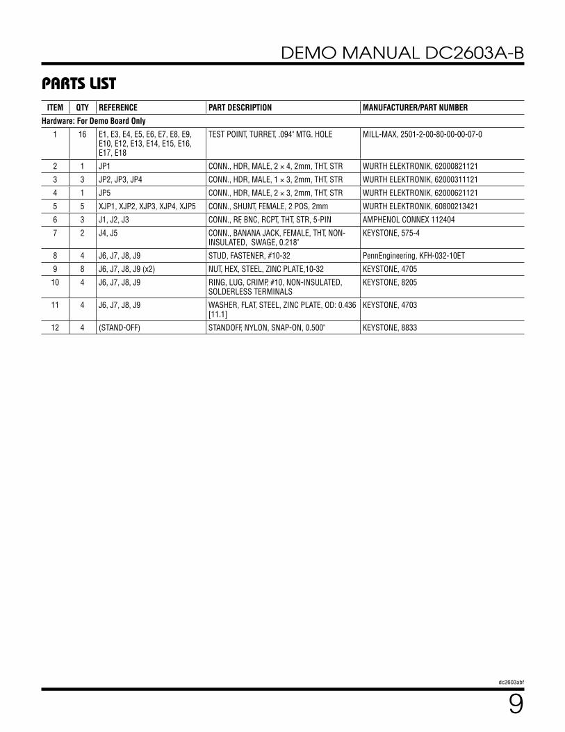
DEMO MANUAL DC2603A-B
PARTS LISTITEM QTY REFERENCE PART DESCRIPTION MANUFACTURER/PART NUMBER
Hardware: For Demo Board Only
1 16 E1, E3, E4, E5, E6, E7, E8, E9, E10, E12, E13, E14, E15, E16, E17, E18
TEST POINT, TURRET, .094" MTG. HOLE MILL-MAX, 2501-2-00-80-00-00-07-0
2 1 JP1 CONN., HDR, MALE, 2 × 4, 2mm, THT, STR WURTH ELEKTRONIK, 62000821121
3 3 JP2, JP3, JP4 CONN., HDR, MALE, 1 × 3, 2mm, THT, STR WURTH ELEKTRONIK, 62000311121
4 1 JP5 CONN., HDR, MALE, 2 × 3, 2mm, THT, STR WURTH ELEKTRONIK, 62000621121
5 5 XJP1, XJP2, XJP3, XJP4, XJP5 CONN., SHUNT, FEMALE, 2 POS, 2mm WURTH ELEKTRONIK, 60800213421
6 3 J1, J2, J3 CONN., RF, BNC, RCPT, THT, STR, 5-PIN AMPHENOL CONNEX 112404
7 2 J4, J5 CONN., BANANA JACK, FEMALE, THT, NON-INSULATED, SWAGE, 0.218"
KEYSTONE, 575-4
8 4 J6, J7, J8, J9 STUD, FASTENER, #10-32 PennEngineering, KFH-032-10ET
9 8 J6, J7, J8, J9 (x2) NUT, HEX, STEEL, ZINC PLATE,10-32 KEYSTONE, 4705
10 4 J6, J7, J8, J9 RING, LUG, CRIMP, #10, NON-INSULATED, SOLDERLESS TERMINALS
KEYSTONE, 8205
11 4 J6, J7, J8, J9 WASHER, FLAT, STEEL, ZINC PLATE, OD: 0.436 [11.1]
KEYSTONE, 4703
12 4 (STAND-OFF) STANDOFF, NYLON, SNAP-ON, 0.500" KEYSTONE, 8833
10dc2603abf
DEMO MANUAL DC2603A-B
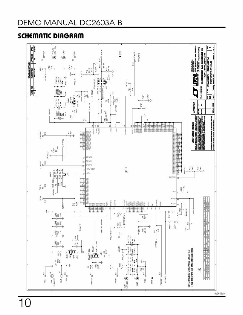
SCHEMATIC DIAGRAM5 5
4 4
3 3
2 2
1 1
DD
CC
BB
AA
VIN
+
VIN
-
VIN
GN
D
4.5V
-20V
VO
1+
VO
1-
VO
2-
VO
2+
ON
TRA
CK
1
ON
EX
T.S
OFT
-STA
RT
TRA
CK
1 S
EL.
NOTE
: UNL
ESS
OTHE
RWIS
E SP
ECIF
IED
1. A
LL R
ESIS
TORS
AND
CAP
ACITO
RS A
RE 06
03.
m
SW
2
SW
1
* U1ASSY
LTM4650AEY
‐A ‐B
C10
OPT
220pF
R46,R47
OPT
10K
LTM4650AEY‐1
C12
OPT
47pF
C17
OPT
3.3nF
C18
OPT
4.7nF
C6,C9
OPT
33pF
COUT9,10,12,18
330uF(7343)
OPT
COUT2,6,13,14,15,16
100uF(1210)
330uF(1210)
VO
UT1
VIN
INTV
CC
VO
1+
VO
1-
INTV
CC
VO
1-
VO
1+
INTV
CC
VO
UT1
VO
2+
VO
2-V
IN
INTV
CC
INTV
CC
DIF
FP
CO
MP
1
VFB
1
DIF
FN
DIF
FOU
T
VO
UT1
S
VO
UT1
TRA
CK
1
RU
N1
VO
2+
VO
UT2
VO
2-
VO
UT2
SR
UN
2
TRA
CK
2
VFB
2
CO
MP
2
INTV
CC
TEM
P
REVI
SION
HIS
TORY
DESC
RIPT
ION
DATE
APPR
OVED
ECO
REV
PROT
OTYP
E1
03-2
8-17
__ST
REVI
SION
HIS
TORY
DESC
RIPT
ION
DATE
APPR
OVED
ECO
REV
PROT
OTYP
E1
03-2
8-17
__ST
REVI
SION
HIS
TORY
DESC
RIPT
ION
DATE
APPR
OVED
ECO
REV
PROT
OTYP
E1
03-2
8-17
__ST
SIZE
DATE
:
IC N
O.RE
V.
SHEE
TOF
TITL
E:
APPR
OVAL
S
PCB
DES.
APP
ENG.
TEC
HN
OLO
GY
Fax:
(408
)434
-050
7
Milp
itas,
CA 95
035
Phon
e: (4
08)4
32-1
900
1630
McC
arth
y Blvd
.
LTC
Conf
iden
tial-F
or C
usto
mer
Use
Onl
y
CUST
OMER
NOT
ICE
LINE
AR T
ECHN
OLOG
Y HA
S MA
DE A
BES
T EF
FORT
TO
DESI
GN A
CIRC
UIT
THAT
MEE
TS C
USTO
MER-
SUPP
LIED
SPE
CIFI
CATI
ONS;
HOW
EVER
, IT R
EMAI
NS T
HE C
USTO
MER'
S RE
SPON
SIBI
LITY
TO
VERI
FY P
ROPE
R AN
D RE
LIAB
LE O
PERA
TION
IN T
HE A
CTUA
LAP
PLIC
ATIO
N. C
OMPO
NENT
SUB
STIT
UTIO
N AN
D PR
INTE
DCI
RCUI
T BO
ARD
LAYO
UT M
AY S
IGNI
FICA
NTLY
AFF
ECT
CIRC
UIT
PERF
ORMA
NCE
OR R
ELIA
BILI
TY. C
ONTA
CT L
INEA
RTE
CHNO
LOGY
APP
LICA
TION
S EN
GINE
ERIN
G FO
R AS
SIST
ANCE
.
THIS
CIR
CUIT
IS P
ROPR
IETA
RY T
O LI
NEAR
TEC
HNOL
OGY
AND
SCHE
MAT
IC
SUPP
LIED
FOR
USE
WIT
H LI
NEAR
TEC
HNOL
OGY
PART
S.SC
ALE
= NO
NE
www.
linea
r.com 1
Tues
day,
March
28, 2
017
12
DC/D
C
MOD
ULE
REGU
LATO
R
LT ST
N/A
LTM4
650A
EY / L
TM46
50AE
Y-1
DEMO
CIR
CUIT
2603
A(A,
B)
HIGH
EFF
ICIE
NCY,
DUA
L 25
A OR
SIN
GLE
50A,
E15
TEM
P
JP3
OFF
RU
N2
13
2
R16
OP
T
E4
CO
UT1
4*
6.3V
1210
C10
*E
7
CO
UT1
3*
6.3V
CO
UT6
*6.
3V12
10
CO
UT2
*6.
3V
CIN
422
uF
1210
25V
E1J4
R3
10
C5
0.1u
F
R19
13.3
K
U1
*VINJ9 VINJ10 VINJ11 VINK2 VINK3 VINK4 VINK9 VINK10 VINK11
VIN
M2
VIN
M3
VIN
M4
VIN
M5
VIN
M6
VIN
M7
VIN
M8
VIN
M9
VIN
M10
VIN
M11
VINL2 VINL3 VINL4 VINL5 VINL6 VINL7 VINL8 VINL9
VIN
L10
VIN
L11
VINJ2 VINJ3 VINJ4
RU
N1
F5
TRA
CK
1E
5
VO
UT1
SC
5
VO
UT1
A1
VO
UT1
A2
VO
UT1
A3
VO
UT1
A4
VO
UT1
A5
VFB
1D
5
SW
1G
2
PG
OO
D1
G9
CO
MP
1E
6
DIF
FOU
TF8
DIFFN E9
DIFFP E8
FSET C6
PHASMD G4
GND A6GND A7GND B6GND B7GND D1GND D2GND D3GND D4GND D9GND D10GND D11GND D12GND E1GND E2GND E3GND E4GND E10GND E11GND E12GND F1GND F2GND F3GND F10GND F11GND F12GND G1
GND G10GND G12GND H1GND H2
GN
DH
3G
ND
H4
GN
DH
5G
ND
H6
GN
DH
7G
ND
H9
GN
DH
10G
ND
H11
GN
DH
12G
ND
J1G
ND
J5G
ND
J8G
ND
J12
GN
DK
1G
ND
K5
GN
DK
6G
ND
K7
GN
DK
8G
ND
K12
GN
DL1
GN
DL1
2G
ND
M1
GN
DM
12S
GN
DC
7S
GN
DD
6S
GN
DF6
SG
ND
F7S
GN
DG
6S
GN
DG
7V
OU
T1B
1V
OU
T1B
2V
OU
T1B
3V
OU
T1B
4V
OU
T1B
5V
OU
T1C
1V
OU
T1C
2V
OU
T1C
3V
OU
T1C
4
CO
MP
2E
7
PG
OO
D2
G8
SW
2G
11
VFB
2D
7
TRA
CK
2D
8R
UN
2F9
VO
UT2
SC
8
TEMPJ6
MODE-PLLINF4
CLKOUTG5
INTVCCH8
EXTVCCJ7
VOUT2A8VOUT2A9VOUT2A10VOUT2A11VOUT2A12VOUT2B8VOUT2B9VOUT2B10VOUT2B11VOUT2B12VOUT2C9VOUT2C10VOUT2C11VOUT2C12
GND G3
R30
147K
J61.
5V /
25A
VO
UT1
J5
JP1
EX
T_C
LK
PS
CC
M
MO
DE
BM
1 3
2 4 65 7
8
R10
6.04
K
C3 OP
TC
4O
PT
+C
OU
T1
OP
T6.
3V
E12
PG
OO
D2
R46
*
C7
0.1u
F
JP5
VO
UT1TR
AC
K2
SE
L.
1 3
2 4
56
R32 0
R15
60.4
K
CIN
322
uF25
V12
10
E13
EX
TVC
C
+ CO
UT1
0*
6.3V
7343
+C
OU
T18 *
6.3V
7343
+CO
UT1
7
OP
T73
43
C6*
R1
10
CO
UT1
6*
6.3V
CO
UT1
5*
6.3V
1210
R22
10
C1
4.7u
F
R7
0
E14
CLK
OU
T
CO
UT4
100u
F6.
3V
1210
R21 0
CIN
222
uF25
V12
10
E6
R42
OP
T
E8
R20
OP
T
R47
*
C2
1uF
CIN
522
uF25
V12
10
+CO
UT7
OP
T73
43
R27
10K
J9G
ND
C12
*
R24
10K
R41
OP
T
R6
OP
T
R2
OP
T
CO
UT8
100u
F6.
3V
C11
OP
T
R8
OP
T
R5
100K
JP2
OFF
RU
N1
13
2
+CO
UT1
2*
6.3V
7343
E10
TRA
CK
2
R18
60.4
K
C17
*
E9
+C
IN1
330u
F25
V
R9
60.4
K
JP4S
OFT
-STA
RT
TRA
CK
1
3
2
+C
OU
T11
OP
T6.
3V73
43
R26 10
C9
*
E3
PG
OO
D1
C8
OP
T
R12
60.4
K
J7G
ND
C18
*
R13
6.04
K
CO
UT5
100u
F6.
3V12
10
E5
R29 0
E16
CLK
IN
R4
OP
T
+C
OU
T9*
6.3V
7343
CO
UT3
100u
F6.
3V
1210
R25
40.2
K
J83.
3V /
25A
VO
UT2
11dc2603abf
DEMO MANUAL DC2603A-B
Information furnished by Linear Technology Corporation is believed to be accurate and reliable. However, no responsibility is assumed for its use. Linear Technology Corporation makes no representa-tion that the interconnection of its circuits as described herein will not infringe on existing patent rights.
SCHEMATIC DIAGRAM5 5
4 4
3 3
2 2
1 1
DD
CC
BB
AA
OP
TIO
NA
L JU
MP
ER
FO
R S
ING
LE O
UTP
UT
CO
NFI
GU
RA
TIO
N
DIF
F S
EN
SIN
G S
ELE
CTI
ON
VO
UT1
Load
Tra
nsie
nt C
ircui
t
VO
UT2
m
VIN
TEM
PIN
TVC
C
RU
N1
RU
N2
TRA
CK
1TR
AC
K2
VFB
1V
FB2
CO
MP
1C
OM
P2
VO
2-D
IFFN
VO
2+D
IFFP
VO
UT1
SV
OU
T1
VO
UT2
SD
IFFO
UT
VO
UT1
VO
UT2
VO
UT1
VO
UT2
INTV
CC
SIZE
DATE
:
IC N
O.RE
V.
SHEE
TOF
TITL
E:
APPR
OVAL
S
PCB
DES.
APP
ENG.
TEC
HN
OLO
GY
Fax:
(408
)434
-050
7
Milp
itas,
CA 95
035
Phon
e: (4
08)4
32-1
900
1630
McC
arth
y Blvd
.
LTC
Conf
iden
tial-F
or C
usto
mer
Use
Onl
y
CUST
OMER
NOT
ICE
LINE
AR T
ECHN
OLOG
Y HA
S MA
DE A
BES
T EF
FORT
TO
DESI
GN A
CIRC
UIT
THAT
MEE
TS C
USTO
MER-
SUPP
LIED
SPE
CIFI
CATI
ONS;
HOW
EVER
, IT R
EMAI
NS T
HE C
USTO
MER'
S RE
SPON
SIBI
LITY
TO
VERI
FY P
ROPE
R AN
D RE
LIAB
LE O
PERA
TION
IN T
HE A
CTUA
LAP
PLIC
ATIO
N. C
OMPO
NENT
SUB
STIT
UTIO
N AN
D PR
INTE
DCI
RCUI
T BO
ARD
LAYO
UT M
AY S
IGNI
FICA
NTLY
AFF
ECT
CIRC
UIT
PERF
ORMA
NCE
OR R
ELIA
BILI
TY. C
ONTA
CT L
INEA
RTE
CHNO
LOGY
APP
LICA
TION
S EN
GINE
ERIN
G FO
R AS
SIST
ANCE
.
THIS
CIR
CUIT
IS P
ROPR
IETA
RY T
O LI
NEAR
TEC
HNOL
OGY
AND
SCHE
MAT
IC
SUPP
LIED
FOR
USE
WIT
H LI
NEAR
TEC
HNOL
OGY
PART
S.SC
ALE
= NO
NE
www.
linea
r.com 1
Tues
day,
March
28, 2
017
22
DC/D
C M
ODUL
E RE
GULA
TOR
LT ST
N/A
LTM4
650A
EY / L
TM46
50AE
Y-1
DEMO
CIR
CUIT
2603
A(A,
B)
HIGH
EFF
ICIE
NCY,
DUA
L 25
A OR
SIN
GLE
50A,
R36
10K
E17
IOS
TEP
CLK
J3IO
STE
P
R23
OP
T
R39
OP
TC
131u
F
R35
OP
T20
10 Q1
SU
D50
N04
-8M
8P-4
GE
3
2
1
34
R14
OP
TR48
OP
T
J1C
14 1uF
R11
OP
T
E18
GN
D
R34
0 O
Hm
0.5W
2010
R43
OP
T
2512
R28
OP
T
R45
OP
T25
12
R38
OP
T25
12
R33
OP
T
R17
OP
TC
161u
F
R44
OP
T25
12
R40
OP
T
C15
1uF
R31
OP
T
J2
R37
0.01
02W 25
12
12dc2603abf
DEMO MANUAL DC2603A-B
LINEAR TECHNOLOGY CORPORATION 2017
LT 0617 • PRINTED IN USA
DEMONSTRATION BOARD IMPORTANT NOTICE
Linear Technology Corporation (LTC) provides the enclosed product(s) under the following AS IS conditions:
This demonstration board (DEMO BOARD) kit being sold or provided by Linear Technology is intended for use for ENGINEERING DEVELOPMENT OR EVALUATION PURPOSES ONLY and is not provided by LTC for commercial use. As such, the DEMO BOARD herein may not be complete in terms of required design-, marketing-, and/or manufacturing-related protective considerations, including but not limited to product safety measures typically found in finished commercial goods. As a prototype, this product does not fall within the scope of the European Union directive on electromagnetic compatibility and therefore may or may not meet the technical requirements of the directive, or other regulations.
If this evaluation kit does not meet the specifications recited in the DEMO BOARD manual the kit may be returned within 30 days from the date of delivery for a full refund. THE FOREGOING WARRANTY IS THE EXCLUSIVE WARRANTY MADE BY THE SELLER TO BUYER AND IS IN LIEU OF ALL OTHER WARRANTIES, EXPRESSED, IMPLIED, OR STATUTORY, INCLUDING ANY WARRANTY OF MERCHANTABILITY OR FITNESS FOR ANY PARTICULAR PURPOSE. EXCEPT TO THE EXTENT OF THIS INDEMNITY, NEITHER PARTY SHALL BE LIABLE TO THE OTHER FOR ANY INDIRECT, SPECIAL, INCIDENTAL, OR CONSEQUENTIAL DAMAGES.
The user assumes all responsibility and liability for proper and safe handling of the goods. Further, the user releases LTC from all claims arising from the handling or use of the goods. Due to the open construction of the product, it is the user’s responsibility to take any and all appropriate precautions with regard to electrostatic discharge. Also be aware that the products herein may not be regulatory compliant or agency certified (FCC, UL, CE, etc.).
No License is granted under any patent right or other intellectual property whatsoever. LTC assumes no liability for applications assistance, customer product design, software performance, or infringement of patents or any other intellectual property rights of any kind.
LTC currently services a variety of customers for products around the world, and therefore this transaction is not exclusive.
Please read the DEMO BOARD manual prior to handling the product. Persons handling this product must have electronics training and observe good laboratory practice standards. Common sense is encouraged.
This notice contains important safety information about temperatures and voltages. For further safety concerns, please contact a LTC application engineer.
Mailing Address:
Linear Technology
1630 McCarthy Blvd.
Milpitas, CA 95035
Copyright © 2004, Linear Technology Corporation