LF442 Dual Low Power JFET Input Operational Amplifier ... · LF442 SNOSC03F –APRIL 1999–REVISED...
23
Product Folder Sample & Buy Technical Documents Tools & Software Support & Community LF442 SNOSC03F – APRIL 1999 – REVISED OCTOBER 2014 LF442 Dual Low Power JFET Input Operational Amplifier 1 Features 3 Description The LF442 dual low power operational amplifiers 1• 1/10 Supply Current of a LM1458: 400 μA (Max) provide many of the same AC characteristics as the • Low Input Bias Current: 50 pA (Max) industry standard LM1458 while greatly improving the • Low Input Offset Voltage: 1 mV (Max) DC characteristics of the LM1458. The amplifiers have the same bandwidth, slew rate, and gain (10 kΩ • Low Input Offset Voltage Drift: 7 μV/°C (Typ) load) as the LM1458 and only draw one tenth the • High Gain Bandwidth: 1 MHz supply current of the LM1458. In addition the well • High Slew Rate: 1 V/μs matched high voltage JFET input devices of the LF442 reduce the input bias and offset currents by a • Low Noise Voltage for Low Power: 35 nV/√Hz factor of 10,000 over the LM1458. A combination of • Low Input Noise Current: 0.01 pA/√Hz careful layout design and internal trimming ensures • High Input Impedance: 10 12 Ω very low input offset voltage and voltage drift. The • High Gain V O = ±10V, R L = 10k: 50k (Min) LF442 also has a very low equivalent input noise voltage for a low power amplifier. 2 Applications The LF442 is pin compatible with the LM1458 • High Speed Integrators allowing an immediate 10 times reduction in power drain in many applications. The LF442 should be • Fast D/A Converters used where low power dissipation and good electrical • Sample and Hold Circuits characteristics are the major considerations. Device Information (1) PART NUMBER PACKAGE BODY SIZE (NOM) LF442ACN PDIP (8) 9.59 mm × 6.35 mm LF442AMH TO-99 (8) 8.96 mm Diameter (1) For all available packages, see the orderable addendum at the end of the datasheet. Inverting Amplifier 1 An IMPORTANT NOTICE at the end of this data sheet addresses availability, warranty, changes, use in safety-critical applications, intellectual property matters and other important disclaimers. PRODUCTION DATA.
Transcript of LF442 Dual Low Power JFET Input Operational Amplifier ... · LF442 SNOSC03F –APRIL 1999–REVISED...
Product
Folder
Sample &Buy
Technical
Documents
Tools &
Software
Support &Community
LF442SNOSC03F –APRIL 1999–REVISED OCTOBER 2014
LF442 Dual Low Power JFET Input Operational Amplifier1 Features 3 Description
The LF442 dual low power operational amplifiers1• 1/10 Supply Current of a LM1458: 400 μA (Max)
provide many of the same AC characteristics as the• Low Input Bias Current: 50 pA (Max) industry standard LM1458 while greatly improving the• Low Input Offset Voltage: 1 mV (Max) DC characteristics of the LM1458. The amplifiers
have the same bandwidth, slew rate, and gain (10 kΩ• Low Input Offset Voltage Drift: 7 μV/°C (Typ)load) as the LM1458 and only draw one tenth the• High Gain Bandwidth: 1 MHz supply current of the LM1458. In addition the well
• High Slew Rate: 1 V/μs matched high voltage JFET input devices of theLF442 reduce the input bias and offset currents by a• Low Noise Voltage for Low Power: 35 nV/√Hzfactor of 10,000 over the LM1458. A combination of• Low Input Noise Current: 0.01 pA/√Hzcareful layout design and internal trimming ensures• High Input Impedance: 1012Ω very low input offset voltage and voltage drift. The
• High Gain VO = ±10V, RL = 10k: 50k (Min) LF442 also has a very low equivalent input noisevoltage for a low power amplifier.
2 Applications The LF442 is pin compatible with the LM1458• High Speed Integrators allowing an immediate 10 times reduction in power
drain in many applications. The LF442 should be• Fast D/A Convertersused where low power dissipation and good electrical• Sample and Hold Circuits characteristics are the major considerations.
Device Information(1)
PART NUMBER PACKAGE BODY SIZE (NOM)LF442ACN PDIP (8) 9.59 mm × 6.35 mmLF442AMH TO-99 (8) 8.96 mm Diameter
(1) For all available packages, see the orderable addendum atthe end of the datasheet.
Inverting Amplifier
1
An IMPORTANT NOTICE at the end of this data sheet addresses availability, warranty, changes, use in safety-critical applications,intellectual property matters and other important disclaimers. PRODUCTION DATA.
LF442SNOSC03F –APRIL 1999–REVISED OCTOBER 2014 www.ti.com
Table of Contents7.2 Functional Block Diagram ....................................... 111 Features .................................................................. 17.3 Feature Description................................................. 112 Applications ........................................................... 17.4 Device Functional Modes........................................ 123 Description ............................................................. 1
8 Application and Implementation ........................ 134 Revision History..................................................... 28.1 Application Information............................................ 135 Pin Configuration and Functions ......................... 38.2 Typical Applications ............................................... 136 Specifications......................................................... 4
9 Power Supply Recommendations ...................... 186.1 Absolute Maximum Ratings ...................................... 410 Layout................................................................... 186.2 Absolute Maximum Ratings (1) (2) ............................... 4
10.1 Layout Guidelines ................................................. 186.3 Handling Ratings ...................................................... 410.2 Layout Example .................................................... 186.4 Recommended Operating Conditions....................... 4
11 Device and Documentation Support ................. 196.5 Thermal Information ................................................. 411.1 Trademarks ........................................................... 196.6 DC Electrical Characteristics (2) ................................. 511.2 Electrostatic Discharge Caution............................ 196.7 AC Electrical Characteristics (3) (2) ............................. 511.3 Glossary ................................................................ 196.8 Typical Performance Characteristics ........................ 6
12 Mechanical, Packaging, and Orderable7 Detailed Description ............................................ 11Information ........................................................... 197.1 Overview ................................................................. 11
4 Revision HistoryNOTE: Page numbers for previous revisions may differ from page numbers in the current version.
Changes from Revision E (October 2013) to Revision F Page
• Deleted Max ΔVOS/ΔT specification for LF442A. ..................................................................................................................... 5
Changes from Revision D (March 2013) to Revision E Page
• Changed Input Noise Voltage units ........................................................................................................................................ 5
Changes from Revision C (March 2013) to Revision D Page
• Changed layout of data sheet from National to TI format ..................................................................................................... 1
2 Submit Documentation Feedback Copyright © 1999–2014, Texas Instruments Incorporated
Product Folder Links: LF442
LF442www.ti.com SNOSC03F –APRIL 1999–REVISED OCTOBER 2014
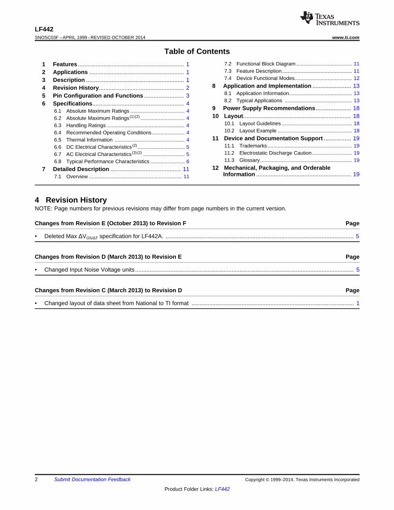
5 Pin Configuration and Functions
TO PackageSee Package Number LMC0008C
Top View
Pin 4 connected to case
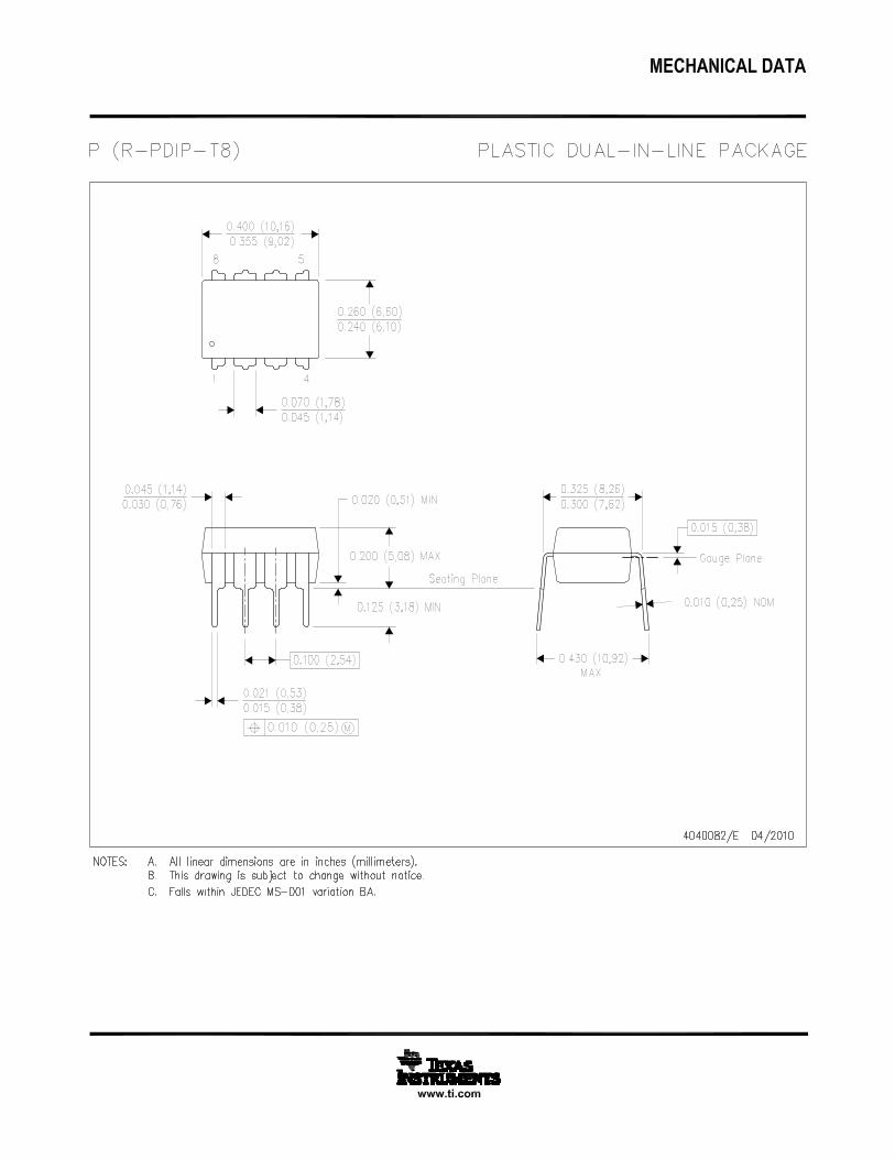
PDIP PackageSee Package Number P0008E
Top View
Pin FunctionsPIN
I/O DESCRIPTIONNAME NO.Output A 1 Output Amplifier A OutputInverting Input A 2 Input Amplifier A Inverting InputNon-Inverting 3 Input Amplifier A Non-Inverting InputInput AV- 4 Power Negative SupplyNon-Inverting 5 Input Amplifier B Non-Inverting InputInput BInverting Input B 6 Input Amplifier B Inverting InputOutput B 7 Output Amplifier B OutputV+ 8 Power Positive Supply
Copyright © 1999–2014, Texas Instruments Incorporated Submit Documentation Feedback 3
Product Folder Links: LF442
LF442SNOSC03F –APRIL 1999–REVISED OCTOBER 2014 www.ti.com
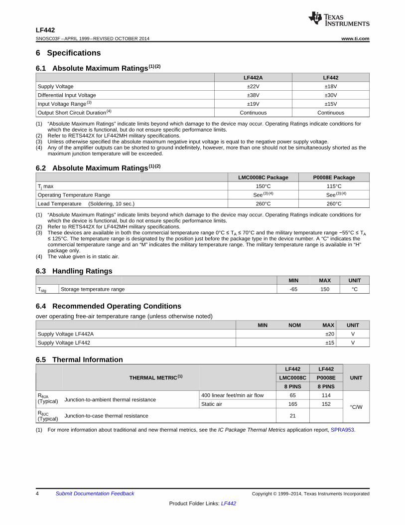
6 Specifications
6.1 Absolute Maximum Ratings (1) (2)
LF442A LF442Supply Voltage ±22V ±18VDifferential Input Voltage ±38V ±30VInput Voltage Range (3) ±19V ±15VOutput Short Circuit Duration (4) Continuous Continuous
(1) “Absolute Maximum Ratings” indicate limits beyond which damage to the device may occur. Operating Ratings indicate conditions forwhich the device is functional, but do not ensure specific performance limits.
(2) Refer to RETS442X for LF442MH military specifications.(3) Unless otherwise specified the absolute maximum negative input voltage is equal to the negative power supply voltage.(4) Any of the amplifier outputs can be shorted to ground indefinitely, however, more than one should not be simultaneously shorted as the
maximum junction temperature will be exceeded.
6.2 Absolute Maximum Ratings (1) (2)
LMC0008C Package P0008E PackageTj max 150°C 115°COperating Temperature Range See (3) (4) See (3) (4)
Lead Temperature (Soldering, 10 sec.) 260°C 260°C
(1) “Absolute Maximum Ratings” indicate limits beyond which damage to the device may occur. Operating Ratings indicate conditions forwhich the device is functional, but do not ensure specific performance limits.
(2) Refer to RETS442X for LF442MH military specifications.(3) These devices are available in both the commercial temperature range 0°C ≤ TA ≤ 70°C and the military temperature range −55°C ≤ TA
≤ 125°C. The temperature range is designated by the position just before the package type in the device number. A “C” indicates thecommercial temperature range and an “M” indicates the military temperature range. The military temperature range is available in “H”package only.
(4) The value given is in static air.
6.3 Handling RatingsMIN MAX UNIT
Tstg Storage temperature range -65 150 °C
6.4 Recommended Operating Conditionsover operating free-air temperature range (unless otherwise noted)
MIN NOM MAX UNITSupply Voltage LF442A ±20 VSupply Voltage LF442 ±15 V
6.5 Thermal InformationLF442 LF442
THERMAL METRIC (1) LMC0008C P0008E UNIT8 PINS 8 PINS
RθJA 400 linear feet/min air flow 65 114Junction-to-ambient thermal resistance(Typical) Static air 165 152 °C/W
RθJC Junction-to-case thermal resistance 21(Typical)
(1) For more information about traditional and new thermal metrics, see the IC Package Thermal Metrics application report, SPRA953.
4 Submit Documentation Feedback Copyright © 1999–2014, Texas Instruments Incorporated
Product Folder Links: LF442

LF442www.ti.com SNOSC03F –APRIL 1999–REVISED OCTOBER 2014
6.6 DC Electrical Characteristics (1) (2)
LF442A LF442PARAMETER TEST CONDITIONS UNIT
MIN TYP MAX MIN TYP MAXVOS Input Offset Voltage RS = 10 kΩ, TA = 25°C 0.5 1.0 1.0 5.0 mV
Over Temperature 7.5 mVΔVOS/ΔT Average TC of Input Offset RS = 10 kΩ 7 7 μV/°CVoltageIOS Input Offset Current VS = ±15V (1) (3) Tj = 25°C 5 25 5 50 pA
Tj = 70°C 1.5 1.5 nATj = 125°C 10 nA
IB Input Bias Current VS = ±15V (1) (3) Tj = 25°C 10 50 10 100 pATj = 70°C 3 3 nATj = 125°C 20 nA
RIN Input Resistance Tj = 25°C 1012 1012 ΩAVOL Large Signal Voltage Gain VS = ±15V, VO = ±10V, 50 200 25 200 V/mVRL = 10 kΩ, TA = 25°C
Over Temperature 25 200 15 200 V/mVVO Output Voltage Swing VS = ±15V, RL = 10 kΩ ±12 ±13 ±12 ±13 VVCM Input Common-Mode ±16 +18 ±11 +14 V
Voltage Range −17 −12 VCMRR Common-Mode Rejection RS ≤ 10 kΩ 80 100 70 95 dBRatioPSRR Supply Voltage Rejection See (4)
80 100 70 90 dBRatioIS Supply Current 300 400 400 500 μA
(1) Unless otherwise specified, the specifications apply over the full temperature range and for VS = ±20V for the LF442A and for VS = ±15Vfor the LF442. VOS, IB, and IOS are measured at VCM = 0.
(2) Refer to RETS442X for LF442MH military specifications.(3) The input bias currents are junction leakage currents which approximately double for every 10°C increase in the junction temperature,
Tj. Due to limited production test time, the input bias currents measured are correlated to junction temperature. In normal operation thejunction temperature rises above the ambient temperature as a result of internal power dissipation, PD. Tj = TA + θjAPD where θjA is thethermal resistance from junction to ambient. Use of a heat sink is recommended if input bias current is to be kept to a minimum.
(4) Supply voltage rejection ratio is measured for both supply magnitudes increasing or decreasing simultaneously in accordance withcommon practice from ±15V to ±5V for the LF442 and ±20V to ±5V for the LF442A.
6.7 AC Electrical Characteristics (1) (2)
LF442A LF442PARAMETER TEST CONDITIONS UNIT
MIN TYP MAX MIN TYP MAXAmplifier to Amplifier Coupling TA = 25°C, f = 1 Hz-20 kHz (Input −120 −120 dBReferred)
SR Slew Rate VS = ±15V, TA = 25°C 0.8 1 0.6 1 V/μsGBW Gain-Bandwidth Product VS = ±15V, TA = 25°C 0.8 1 0.6 1 MHzen Equivalent Input Noise Voltage TA = 25°C, RS = 100Ω, f = 1 kHz 35 35 nV/√Hzin Equivalent Input Noise Current TA = 25°C, f = 1 kHz 0.01 0.01 pA/√Hz
(1) Unless otherwise specified, the specifications apply over the full temperature range and for VS = ±20V for the LF442A and for VS = ±15Vfor the LF442. VOS, IB, and IOS are measured at VCM = 0.
(2) Refer to RETS442X for LF442MH military specifications.
Copyright © 1999–2014, Texas Instruments Incorporated Submit Documentation Feedback 5
Product Folder Links: LF442
LF442SNOSC03F –APRIL 1999–REVISED OCTOBER 2014 www.ti.com
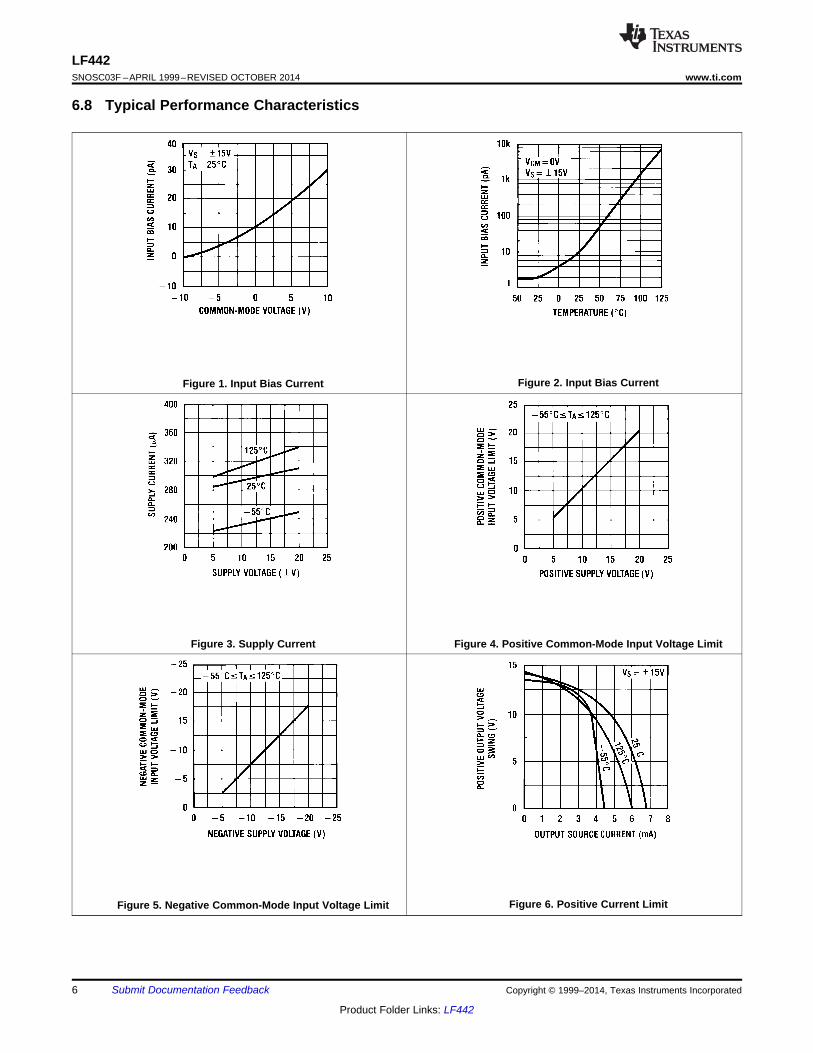
6.8 Typical Performance Characteristics
Figure 2. Input Bias CurrentFigure 1. Input Bias Current
Figure 3. Supply Current Figure 4. Positive Common-Mode Input Voltage Limit
Figure 6. Positive Current LimitFigure 5. Negative Common-Mode Input Voltage Limit
6 Submit Documentation Feedback Copyright © 1999–2014, Texas Instruments Incorporated
Product Folder Links: LF442
LF442www.ti.com SNOSC03F –APRIL 1999–REVISED OCTOBER 2014
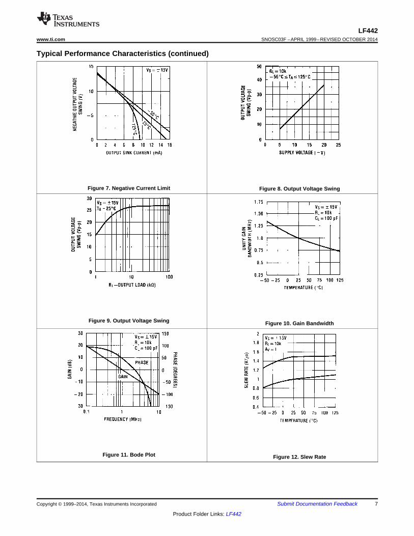
Typical Performance Characteristics (continued)
Figure 7. Negative Current Limit Figure 8. Output Voltage Swing
Figure 9. Output Voltage Swing Figure 10. Gain Bandwidth
Figure 11. Bode Plot Figure 12. Slew Rate
Copyright © 1999–2014, Texas Instruments Incorporated Submit Documentation Feedback 7
Product Folder Links: LF442
LF442SNOSC03F –APRIL 1999–REVISED OCTOBER 2014 www.ti.com
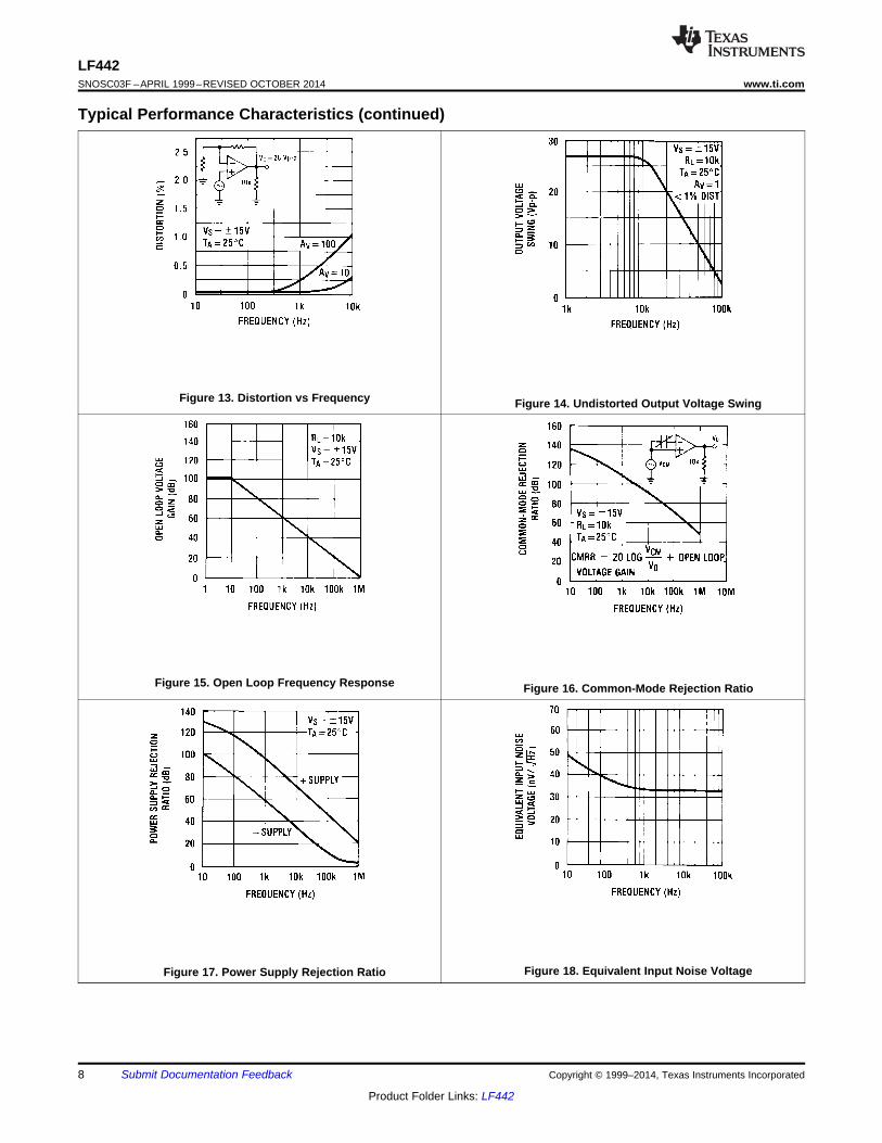
Typical Performance Characteristics (continued)
Figure 13. Distortion vs Frequency Figure 14. Undistorted Output Voltage Swing
Figure 15. Open Loop Frequency Response Figure 16. Common-Mode Rejection Ratio
Figure 18. Equivalent Input Noise VoltageFigure 17. Power Supply Rejection Ratio
8 Submit Documentation Feedback Copyright © 1999–2014, Texas Instruments Incorporated
Product Folder Links: LF442
LF442www.ti.com SNOSC03F –APRIL 1999–REVISED OCTOBER 2014
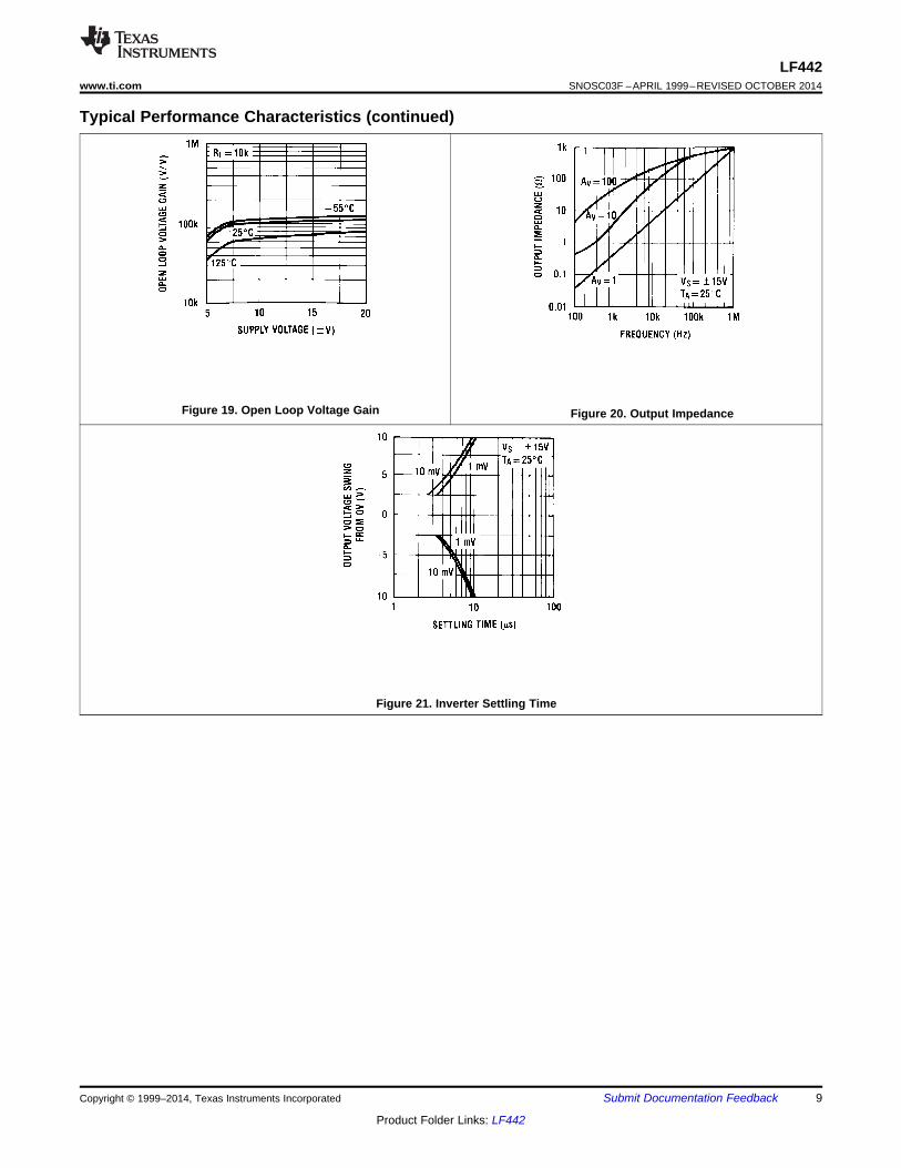
Typical Performance Characteristics (continued)
Figure 19. Open Loop Voltage Gain Figure 20. Output Impedance
Figure 21. Inverter Settling Time
Copyright © 1999–2014, Texas Instruments Incorporated Submit Documentation Feedback 9
Product Folder Links: LF442

LF442SNOSC03F –APRIL 1999–REVISED OCTOBER 2014 www.ti.com
6.8.1 Pulse ResponseRL = 10 kΩ, CL = 10 pF
Figure 22. Small Signal InvertingFigure 23. Small Signal Non-Inverting
Figure 24. Large Signal Inverting Figure 25. Large Signal Non-Inverting
10 Submit Documentation Feedback Copyright © 1999–2014, Texas Instruments Incorporated
Product Folder Links: LF442
LF442www.ti.com SNOSC03F –APRIL 1999–REVISED OCTOBER 2014
7 Detailed Description
7.1 OverviewThe LF442 dual low power operational amplifiers provide many of the same AC characteristics as the industrystandard LM1458 while greatly improving the DC characteristics of the LM1458. The amplifiers have the samebandwidth, slew rate, and gain (10 kΩ load) as the LM1458 and only draw one tenth the supply current of theLM1458. In addition the well matched high voltage JFET input devices of the LF442 reduce the input bias andoffset currents by a factor of 10,000 over the LM1458. A combination of careful layout design and internaltrimming ensures very low input offset voltage and voltage drift. The LF442 also has a very low equivalent inputnoise voltage for a low power amplifier.
The LF442 is pin compatible with the LM1458 allowing an immediate 10 times reduction in power drain in manyapplications. The LF442 should be used where low power dissipation and good electrical characteristics are themajor considerations.
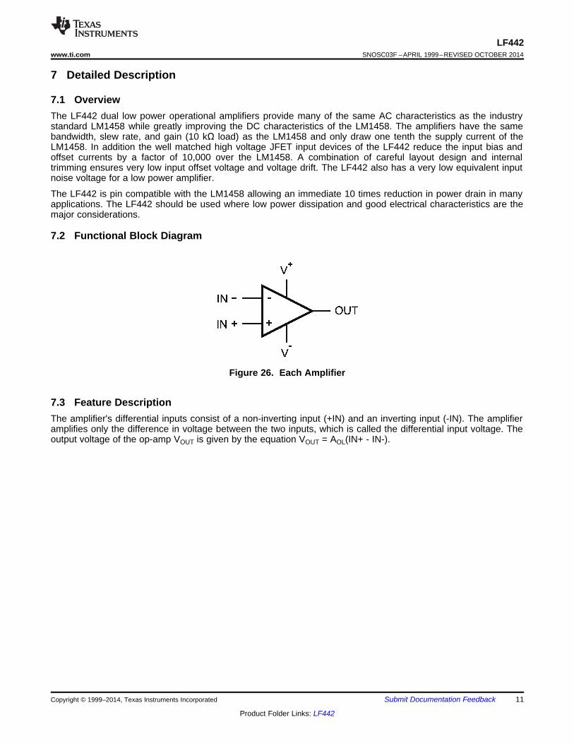
7.2 Functional Block Diagram
Figure 26. Each Amplifier
7.3 Feature DescriptionThe amplifier's differential inputs consist of a non-inverting input (+IN) and an inverting input (-IN). The amplifieramplifies only the difference in voltage between the two inputs, which is called the differential input voltage. Theoutput voltage of the op-amp VOUT is given by the equation VOUT = AOL(IN+ - IN-).
Copyright © 1999–2014, Texas Instruments Incorporated Submit Documentation Feedback 11
Product Folder Links: LF442
LF442SNOSC03F –APRIL 1999–REVISED OCTOBER 2014 www.ti.com
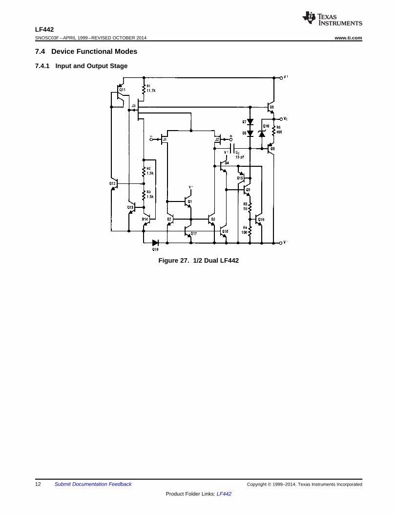
7.4 Device Functional Modes
7.4.1 Input and Output Stage
Figure 27. 1/2 Dual LF442
12 Submit Documentation Feedback Copyright © 1999–2014, Texas Instruments Incorporated
Product Folder Links: LF442
LF442www.ti.com SNOSC03F –APRIL 1999–REVISED OCTOBER 2014
8 Application and Implementation
NOTEInformation in the following applications sections is not part of the TI componentspecification, and TI does not warrant its accuracy or completeness. TI’s customers areresponsible for determining suitability of components for their purposes. Customers shouldvalidate and test their design implementation to confirm system functionality.
8.1 Application InformationThe LF442 uses a combination of careful layout design and internal trimming to ensure very low input offsetvoltage and voltage drift. The LF442 also has a very low equivalent input noise voltage for a low power amplifier.The LF442 should be used where low power dissipation and good electrical characteristics are the majorconsiderations.
8.2 Typical Applications1. Battery Powered Strip Chart Preamplifier2. "No FET" Low Power V to F Converter3. High Efficiency Crystal Oven Controller4. Conventional Log Amplifier5. Unconvential Log Amplifier
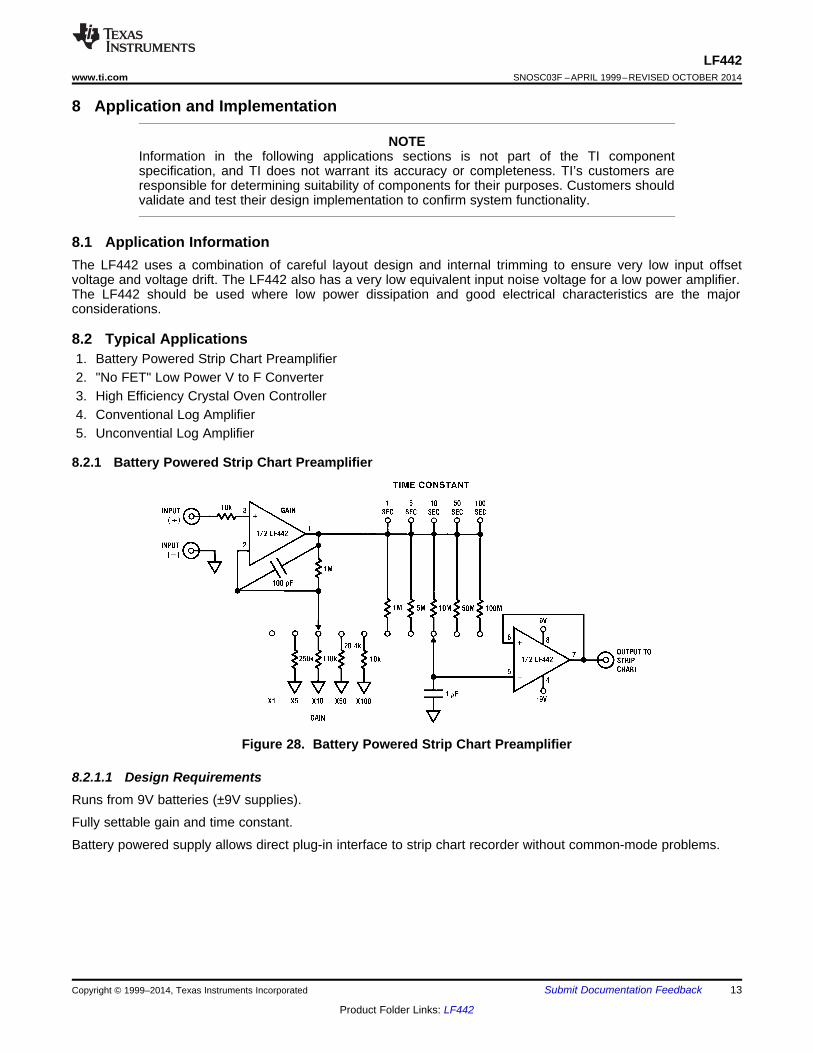
8.2.1 Battery Powered Strip Chart Preamplifier
Figure 28. Battery Powered Strip Chart Preamplifier
8.2.1.1 Design RequirementsRuns from 9V batteries (±9V supplies).
Fully settable gain and time constant.
Battery powered supply allows direct plug-in interface to strip chart recorder without common-mode problems.
Copyright © 1999–2014, Texas Instruments Incorporated Submit Documentation Feedback 13
Product Folder Links: LF442
Time (s)
Inpu
t/Out
put (
V)
0 2 4 6 8 10 12 14 16 18-2
-1.5
-1
-0.5
0
0.5
1
1.5
2
D001
InputOutput
LF442SNOSC03F –APRIL 1999–REVISED OCTOBER 2014 www.ti.com
Typical Applications (continued)8.2.1.2 Detailed Design ProcedureThis device is a dual low power op amp with internally trimmed input offset voltages and JFET input devices (BI-FET II). These JFETs have large reverse breakdown voltages from gate to source and drain eliminating the needfor clamps across the inputs. Therefore, large differential input voltages can easily be accommodated without alarge increase in input current. The maximum differential input voltage is independent of the supply voltages.However, neither of the input voltages should be allowed to exceed the negative supply as this will cause largecurrents to flow which can result in a destroyed unit.
Exceeding the negative common-mode limit on either input will force the output to a high state, potentiallycausing a reversal of phase to the output. Exceeding the negative common-mode limit on both inputs will forcethe amplifier output to a high state. In neither case does a latch occur since raising the input back within thecommon-mode range again puts the input stage and thus the amplifier in a normal operating mode.
Exceeding the positive common-mode limit on a single input will not change the phase of the output; however, ifboth inputs exceed the limit, the output of the amplifier will be forced to a high state.
The amplifiers will operate with a common-mode input voltage equal to the positive supply; however, the gainbandwidth and slew rate may be decreased in this condition. When the negative common-mode voltage swingsto within 3V of the negative supply, an increase in input offset voltage may occur.
Each amplifier is individually biased to allow normal circuit operation with power supplies of ±3.0V. Supplyvoltages less than these may degrade the common-mode rejection and restrict the output voltage swing.
The amplifiers will drive a 10 kΩ load resistance to ± 10V over the full temperature range.
Precautions should be taken to ensure that the power supply for the integrated circuit never becomes reversed inpolarity or that the unit is not inadvertently installed backwards in a socket as an unlimited current surge throughthe resulting forward diode within the IC could cause fusing of the internal conductors and result in a destroyedunit.
A feedback pole is created when the feedback around any amplifier is resistive. The parallel resistance andcapacitance from the input of the device (usually the inverting input) to AC ground set the frequency of the pole.In many instances the frequency of this pole is much greater than the expected 3 dB frequency of the closedloop gain and consequenty there is negligible effect on stability margin. However, if the feedback pole is lessthan approximately 6 times the expected 3 dB frequency a lead capacitor should be placed from the output to theinput of the op amp. The value of the added capacitor should be such that the RC time constant of this capacitorand the resistance it parallels is greater than or equal to the original feedback pole time constant.
8.2.1.3 Application Curves
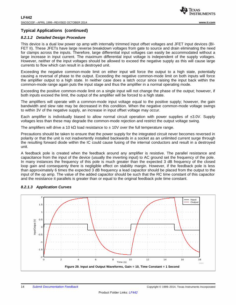
Figure 29. Input and Output Waveforms, Gain = 10, Time Constant = 1 Second
14 Submit Documentation Feedback Copyright © 1999–2014, Texas Instruments Incorporated
Product Folder Links: LF442
Time (s)
Input/O
utp
ut (V
)
0 0.001 0.002 0.003 0.004 0.005 0.006 0.007 0.008 0.009-15
-12
-9
-6
-3
0
3
6
9
12
15
D001
InputOutput
LF442www.ti.com SNOSC03F –APRIL 1999–REVISED OCTOBER 2014
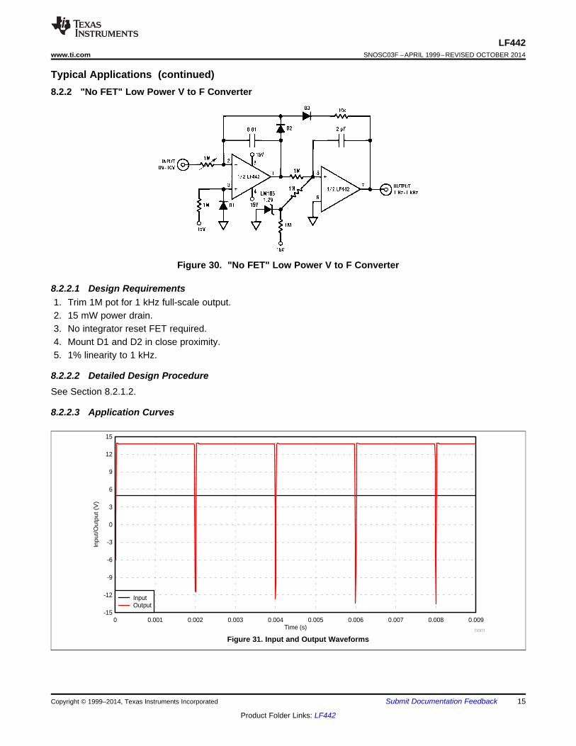
Typical Applications (continued)8.2.2 "No FET" Low Power V to F Converter
Figure 30. "No FET" Low Power V to F Converter
8.2.2.1 Design Requirements1. Trim 1M pot for 1 kHz full-scale output.2. 15 mW power drain.3. No integrator reset FET required.4. Mount D1 and D2 in close proximity.5. 1% linearity to 1 kHz.
8.2.2.2 Detailed Design ProcedureSee Section 8.2.1.2.
8.2.2.3 Application Curves
Figure 31. Input and Output Waveforms
Copyright © 1999–2014, Texas Instruments Incorporated Submit Documentation Feedback 15
Product Folder Links: LF442
LF442SNOSC03F –APRIL 1999–REVISED OCTOBER 2014 www.ti.com
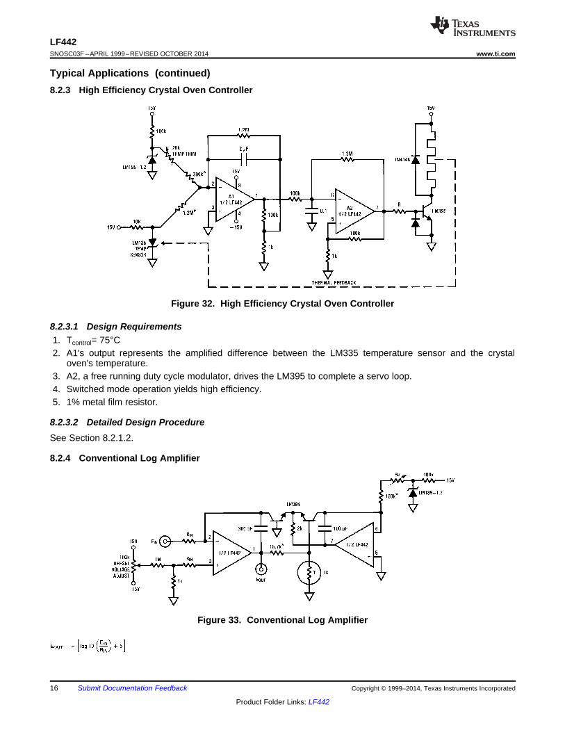
Typical Applications (continued)8.2.3 High Efficiency Crystal Oven Controller
Figure 32. High Efficiency Crystal Oven Controller
8.2.3.1 Design Requirements1. Tcontrol= 75°C2. A1's output represents the amplified difference between the LM335 temperature sensor and the crystal
oven's temperature.3. A2, a free running duty cycle modulator, drives the LM395 to complete a servo loop.4. Switched mode operation yields high efficiency.5. 1% metal film resistor.
8.2.3.2 Detailed Design ProcedureSee Section 8.2.1.2.
8.2.4 Conventional Log Amplifier
Figure 33. Conventional Log Amplifier
16 Submit Documentation Feedback Copyright © 1999–2014, Texas Instruments Incorporated
Product Folder Links: LF442
LF442www.ti.com SNOSC03F –APRIL 1999–REVISED OCTOBER 2014
Typical Applications (continued)8.2.4.1 Design Requirements1. RT = Tel Labs type Q81.2. Trim 5k for 10 μA through the 5k–120k combination.3. *1% film resistor
8.2.4.2 Detailed Design ProcedureSee Section 8.2.1.2.
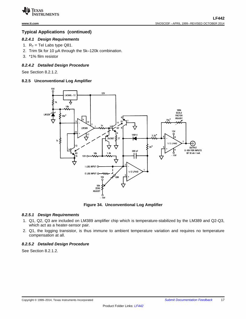
8.2.5 Unconventional Log Amplifier
Figure 34. Unconventional Log Amplifier
8.2.5.1 Design Requirements1. Q1, Q2, Q3 are included on LM389 amplifier chip which is temperature-stabilized by the LM389 and Q2-Q3,
which act as a heater-sensor pair.2. Q1, the logging transistor, is thus immune to ambient temperature variation and requires no temperature
compensation at all.
8.2.5.2 Detailed Design ProcedureSee Section 8.2.1.2.
Copyright © 1999–2014, Texas Instruments Incorporated Submit Documentation Feedback 17
Product Folder Links: LF442
LF442SNOSC03F –APRIL 1999–REVISED OCTOBER 2014 www.ti.com
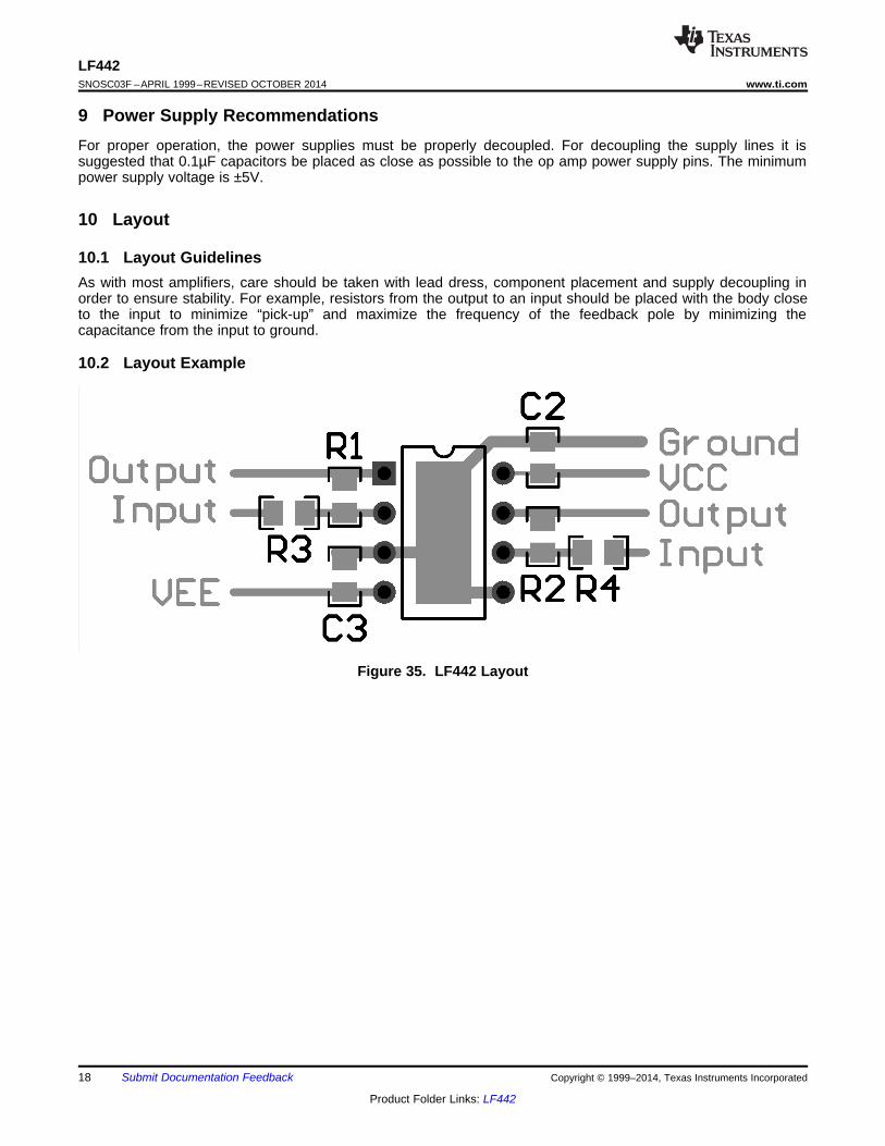
9 Power Supply RecommendationsFor proper operation, the power supplies must be properly decoupled. For decoupling the supply lines it issuggested that 0.1µF capacitors be placed as close as possible to the op amp power supply pins. The minimumpower supply voltage is ±5V.
10 Layout
10.1 Layout GuidelinesAs with most amplifiers, care should be taken with lead dress, component placement and supply decoupling inorder to ensure stability. For example, resistors from the output to an input should be placed with the body closeto the input to minimize “pick-up” and maximize the frequency of the feedback pole by minimizing thecapacitance from the input to ground.
10.2 Layout Example
Figure 35. LF442 Layout
18 Submit Documentation Feedback Copyright © 1999–2014, Texas Instruments Incorporated
Product Folder Links: LF442
LF442www.ti.com SNOSC03F –APRIL 1999–REVISED OCTOBER 2014
11 Device and Documentation Support
11.1 TrademarksAll trademarks are the property of their respective owners.
11.2 Electrostatic Discharge CautionThese devices have limited built-in ESD protection. The leads should be shorted together or the device placed in conductive foamduring storage or handling to prevent electrostatic damage to the MOS gates.
11.3 GlossarySLYZ022 — TI Glossary.
This glossary lists and explains terms, acronyms, and definitions.
12 Mechanical, Packaging, and Orderable InformationThe following pages include mechanical, packaging, and orderable information. This information is the mostcurrent data available for the designated devices. This data is subject to change without notice and revision ofthis document. For browser-based versions of this data sheet, refer to the left-hand navigation.
Copyright © 1999–2014, Texas Instruments Incorporated Submit Documentation Feedback 19
Product Folder Links: LF442

PACKAGE OPTION ADDENDUM
www.ti.com 14-Aug-2017
Addendum-Page 1
PACKAGING INFORMATION
Orderable Device Status(1)
Package Type PackageDrawing
Pins PackageQty
Eco Plan(2)
Lead/Ball Finish(6)
MSL Peak Temp(3)
Op Temp (°C) Device Marking(4/5)
Samples
LF442ACN/NOPB LIFEBUY PDIP P 8 40 Green (RoHS& no Sb/Br)
CU SN Level-1-NA-UNLIM 0 to 70 LF442ACN
LF442CN/NOPB LIFEBUY PDIP P 8 40 Green (RoHS& no Sb/Br)
CU SN Level-1-NA-UNLIM 0 to 70 LF442CN
(1) The marketing status values are defined as follows:ACTIVE: Product device recommended for new designs.LIFEBUY: TI has announced that the device will be discontinued, and a lifetime-buy period is in effect.NRND: Not recommended for new designs. Device is in production to support existing customers, but TI does not recommend using this part in a new design.PREVIEW: Device has been announced but is not in production. Samples may or may not be available.OBSOLETE: TI has discontinued the production of the device.
(2) RoHS: TI defines "RoHS" to mean semiconductor products that are compliant with the current EU RoHS requirements for all 10 RoHS substances, including the requirement that RoHS substancedo not exceed 0.1% by weight in homogeneous materials. Where designed to be soldered at high temperatures, "RoHS" products are suitable for use in specified lead-free processes. TI mayreference these types of products as "Pb-Free".RoHS Exempt: TI defines "RoHS Exempt" to mean products that contain lead but are compliant with EU RoHS pursuant to a specific EU RoHS exemption.Green: TI defines "Green" to mean the content of Chlorine (Cl) and Bromine (Br) based flame retardants meet JS709B low halogen requirements of <=1000ppm threshold. Antimony trioxide basedflame retardants must also meet the <=1000ppm threshold requirement.
(3) MSL, Peak Temp. - The Moisture Sensitivity Level rating according to the JEDEC industry standard classifications, and peak solder temperature.
(4) There may be additional marking, which relates to the logo, the lot trace code information, or the environmental category on the device.
(5) Multiple Device Markings will be inside parentheses. Only one Device Marking contained in parentheses and separated by a "~" will appear on a device. If a line is indented then it is a continuationof the previous line and the two combined represent the entire Device Marking for that device.
(6) Lead/Ball Finish - Orderable Devices may have multiple material finish options. Finish options are separated by a vertical ruled line. Lead/Ball Finish values may wrap to two lines if the finishvalue exceeds the maximum column width.
Important Information and Disclaimer:The information provided on this page represents TI's knowledge and belief as of the date that it is provided. TI bases its knowledge and belief on informationprovided by third parties, and makes no representation or warranty as to the accuracy of such information. Efforts are underway to better integrate information from third parties. TI has taken andcontinues to take reasonable steps to provide representative and accurate information but may not have conducted destructive testing or chemical analysis on incoming materials and chemicals.TI and TI suppliers consider certain information to be proprietary, and thus CAS numbers and other limited information may not be available for release.
In no event shall TI's liability arising out of such information exceed the total purchase price of the TI part(s) at issue in this document sold by TI to Customer on an annual basis.
PACKAGE OPTION ADDENDUM
www.ti.com 14-Aug-2017
Addendum-Page 2

IMPORTANT NOTICE
Texas Instruments Incorporated (TI) reserves the right to make corrections, enhancements, improvements and other changes to itssemiconductor products and services per JESD46, latest issue, and to discontinue any product or service per JESD48, latest issue. Buyersshould obtain the latest relevant information before placing orders and should verify that such information is current and complete.TI’s published terms of sale for semiconductor products (http://www.ti.com/sc/docs/stdterms.htm) apply to the sale of packaged integratedcircuit products that TI has qualified and released to market. Additional terms may apply to the use or sale of other types of TI products andservices.Reproduction of significant portions of TI information in TI data sheets is permissible only if reproduction is without alteration and isaccompanied by all associated warranties, conditions, limitations, and notices. TI is not responsible or liable for such reproduceddocumentation. Information of third parties may be subject to additional restrictions. Resale of TI products or services with statementsdifferent from or beyond the parameters stated by TI for that product or service voids all express and any implied warranties for theassociated TI product or service and is an unfair and deceptive business practice. TI is not responsible or liable for any such statements.Buyers and others who are developing systems that incorporate TI products (collectively, “Designers”) understand and agree that Designersremain responsible for using their independent analysis, evaluation and judgment in designing their applications and that Designers havefull and exclusive responsibility to assure the safety of Designers' applications and compliance of their applications (and of all TI productsused in or for Designers’ applications) with all applicable regulations, laws and other applicable requirements. Designer represents that, withrespect to their applications, Designer has all the necessary expertise to create and implement safeguards that (1) anticipate dangerousconsequences of failures, (2) monitor failures and their consequences, and (3) lessen the likelihood of failures that might cause harm andtake appropriate actions. Designer agrees that prior to using or distributing any applications that include TI products, Designer willthoroughly test such applications and the functionality of such TI products as used in such applications.TI’s provision of technical, application or other design advice, quality characterization, reliability data or other services or information,including, but not limited to, reference designs and materials relating to evaluation modules, (collectively, “TI Resources”) are intended toassist designers who are developing applications that incorporate TI products; by downloading, accessing or using TI Resources in anyway, Designer (individually or, if Designer is acting on behalf of a company, Designer’s company) agrees to use any particular TI Resourcesolely for this purpose and subject to the terms of this Notice.TI’s provision of TI Resources does not expand or otherwise alter TI’s applicable published warranties or warranty disclaimers for TIproducts, and no additional obligations or liabilities arise from TI providing such TI Resources. TI reserves the right to make corrections,enhancements, improvements and other changes to its TI Resources. TI has not conducted any testing other than that specificallydescribed in the published documentation for a particular TI Resource.Designer is authorized to use, copy and modify any individual TI Resource only in connection with the development of applications thatinclude the TI product(s) identified in such TI Resource. NO OTHER LICENSE, EXPRESS OR IMPLIED, BY ESTOPPEL OR OTHERWISETO ANY OTHER TI INTELLECTUAL PROPERTY RIGHT, AND NO LICENSE TO ANY TECHNOLOGY OR INTELLECTUAL PROPERTYRIGHT OF TI OR ANY THIRD PARTY IS GRANTED HEREIN, including but not limited to any patent right, copyright, mask work right, orother intellectual property right relating to any combination, machine, or process in which TI products or services are used. Informationregarding or referencing third-party products or services does not constitute a license to use such products or services, or a warranty orendorsement thereof. Use of TI Resources may require a license from a third party under the patents or other intellectual property of thethird party, or a license from TI under the patents or other intellectual property of TI.TI RESOURCES ARE PROVIDED “AS IS” AND WITH ALL FAULTS. TI DISCLAIMS ALL OTHER WARRANTIES ORREPRESENTATIONS, EXPRESS OR IMPLIED, REGARDING RESOURCES OR USE THEREOF, INCLUDING BUT NOT LIMITED TOACCURACY OR COMPLETENESS, TITLE, ANY EPIDEMIC FAILURE WARRANTY AND ANY IMPLIED WARRANTIES OFMERCHANTABILITY, FITNESS FOR A PARTICULAR PURPOSE, AND NON-INFRINGEMENT OF ANY THIRD PARTY INTELLECTUALPROPERTY RIGHTS. TI SHALL NOT BE LIABLE FOR AND SHALL NOT DEFEND OR INDEMNIFY DESIGNER AGAINST ANY CLAIM,INCLUDING BUT NOT LIMITED TO ANY INFRINGEMENT CLAIM THAT RELATES TO OR IS BASED ON ANY COMBINATION OFPRODUCTS EVEN IF DESCRIBED IN TI RESOURCES OR OTHERWISE. IN NO EVENT SHALL TI BE LIABLE FOR ANY ACTUAL,DIRECT, SPECIAL, COLLATERAL, INDIRECT, PUNITIVE, INCIDENTAL, CONSEQUENTIAL OR EXEMPLARY DAMAGES INCONNECTION WITH OR ARISING OUT OF TI RESOURCES OR USE THEREOF, AND REGARDLESS OF WHETHER TI HAS BEENADVISED OF THE POSSIBILITY OF SUCH DAMAGES.Unless TI has explicitly designated an individual product as meeting the requirements of a particular industry standard (e.g., ISO/TS 16949and ISO 26262), TI is not responsible for any failure to meet such industry standard requirements.Where TI specifically promotes products as facilitating functional safety or as compliant with industry functional safety standards, suchproducts are intended to help enable customers to design and create their own applications that meet applicable functional safety standardsand requirements. Using products in an application does not by itself establish any safety features in the application. Designers mustensure compliance with safety-related requirements and standards applicable to their applications. Designer may not use any TI products inlife-critical medical equipment unless authorized officers of the parties have executed a special contract specifically governing such use.Life-critical medical equipment is medical equipment where failure of such equipment would cause serious bodily injury or death (e.g., lifesupport, pacemakers, defibrillators, heart pumps, neurostimulators, and implantables). Such equipment includes, without limitation, allmedical devices identified by the U.S. Food and Drug Administration as Class III devices and equivalent classifications outside the U.S.TI may expressly designate certain products as completing a particular qualification (e.g., Q100, Military Grade, or Enhanced Product).Designers agree that it has the necessary expertise to select the product with the appropriate qualification designation for their applicationsand that proper product selection is at Designers’ own risk. Designers are solely responsible for compliance with all legal and regulatoryrequirements in connection with such selection.Designer will fully indemnify TI and its representatives against any damages, costs, losses, and/or liabilities arising out of Designer’s non-compliance with the terms and provisions of this Notice.
Mailing Address: Texas Instruments, Post Office Box 655303, Dallas, Texas 75265Copyright © 2017, Texas Instruments Incorporated