Datasheet - STD14NM50NAG - Automotive-grade N-channel 500 ... · 100 Ω 100 nF D.U.T. pulse width +...
16
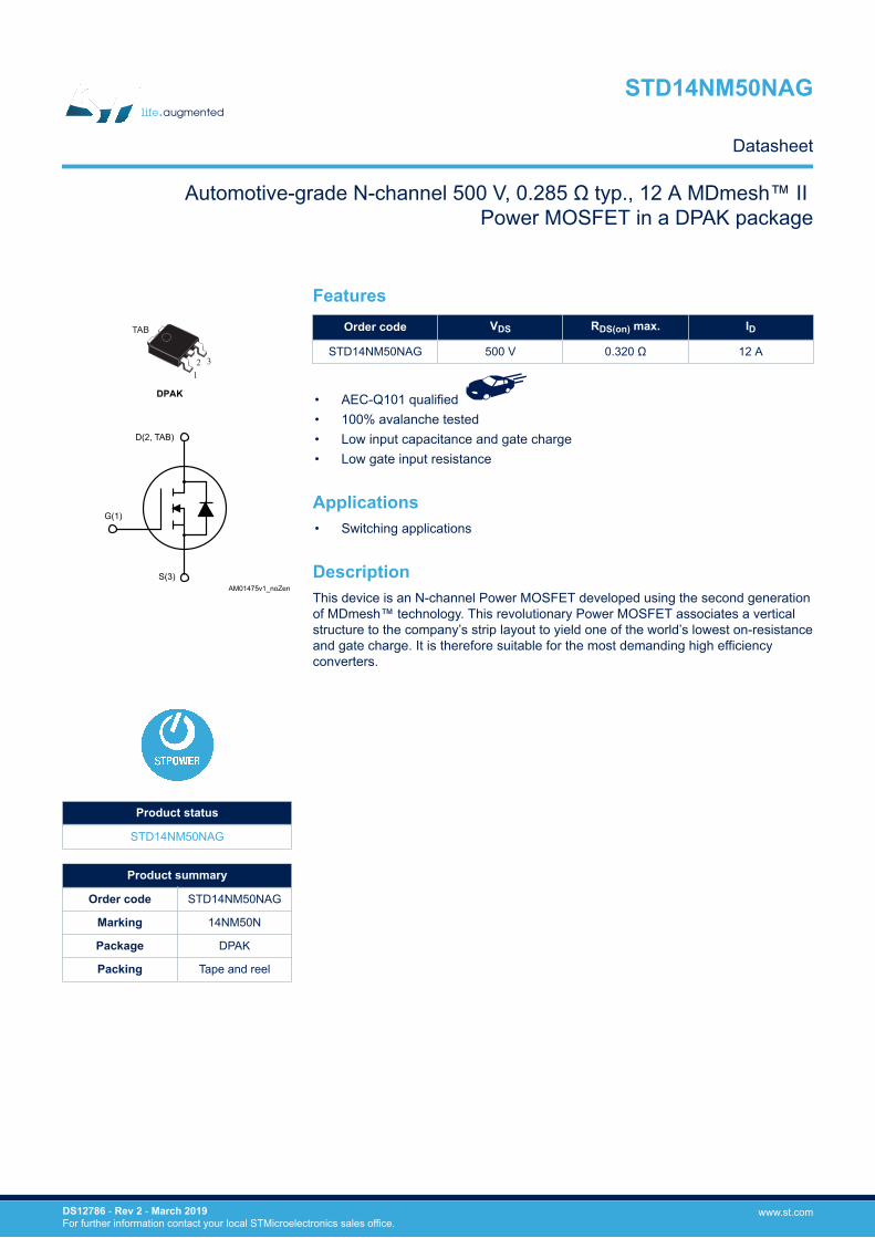
1 3 TAB 2 DPAK AM01475v1_noZen D(2, TAB) G(1) S(3) Features Order code V DS R DS(on) max. I D STD14NM50NAG 500 V 0.320 Ω 12 A • AEC-Q101 qualified • 100% avalanche tested • Low input capacitance and gate charge • Low gate input resistance Applications • Switching applications Description This device is an N-channel Power MOSFET developed using the second generation of MDmesh™ technology. This revolutionary Power MOSFET associates a vertical structure to the company’s strip layout to yield one of the world’s lowest on-resistance and gate charge. It is therefore suitable for the most demanding high efficiency converters. Product status STD14NM50NAG Product summary Order code STD14NM50NAG Marking 14NM50N Package DPAK Packing Tape and reel Automotive-grade N-channel 500 V, 0.285 Ω typ., 12 A MDmesh™ II Power MOSFET in a DPAK package STD14NM50NAG Datasheet DS12786 - Rev 2 - March 2019 For further information contact your local STMicroelectronics sales office. www.st.com
Transcript of Datasheet - STD14NM50NAG - Automotive-grade N-channel 500 ... · 100 Ω 100 nF D.U.T. pulse width +...
13
TAB
2
DPAK
AM01475v1_noZen
D(2, TAB)
G(1)
S(3)
FeaturesOrder code VDS RDS(on) max. ID
STD14NM50NAG 500 V 0.320 Ω 12 A
• AEC-Q101 qualified • 100% avalanche tested• Low input capacitance and gate charge• Low gate input resistance
Applications• Switching applications
DescriptionThis device is an N-channel Power MOSFET developed using the second generationof MDmesh™ technology. This revolutionary Power MOSFET associates a verticalstructure to the company’s strip layout to yield one of the world’s lowest on-resistanceand gate charge. It is therefore suitable for the most demanding high efficiencyconverters.
Product status
STD14NM50NAG
Product summary
Order code STD14NM50NAG
Marking 14NM50N
Package DPAK
Packing Tape and reel
Automotive-grade N-channel 500 V, 0.285 Ω typ., 12 A MDmesh™ II Power MOSFET in a DPAK package
STD14NM50NAG
Datasheet
DS12786 - Rev 2 - March 2019For further information contact your local STMicroelectronics sales office.
www.st.com
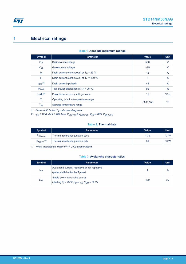
1 Electrical ratings
Table 1. Absolute maximum ratings
Symbol Parameter Value Unit
VDS Drain-source voltage 500 V
VGS Gate-source voltage ±25 V
ID Drain current (continuous) at TC = 25 °C 12 A
ID Drain current (continuous) at TC = 100 °C 8 A
IDM (1) Drain current (pulsed) 48 A
PTOT Total power dissipation at TC = 25 °C 90 W
dv/dt (2) Peak diode recovery voltage slope 15 V/ns
Tj Operating junction temperature range-55 to 150 °C
Tstg Storage temperature range
1. Pulse width limited by safe operating area.2. ISD ≤ 12 A, di/dt ≤ 400 A/μs, VDSpeak ≤ V(BR)DSS, VDD = 80% V(BR)DSS.
Table 2. Thermal data
Symbol Parameter Value Unit
Rthj-case Thermal resistance junction-case 1.39 °C/W
Rthj-pcb (1) Thermal resistance junction-pcb 50 °C/W
1. When mounted on 1inch² FR-4, 2 Oz copper board.
Table 3. Avalanche characteristics
Symbol Parameter Value Unit
IARAvalanche current, repetitive or not-repetitive
(pulse width limited by Tj max)4 A
EASSingle pulse avalanche energy
(starting Tj = 25 °C, ID = IAS, VDD = 50 V)172 mJ
STD14NM50NAGElectrical ratings
DS12786 - Rev 2 page 2/16
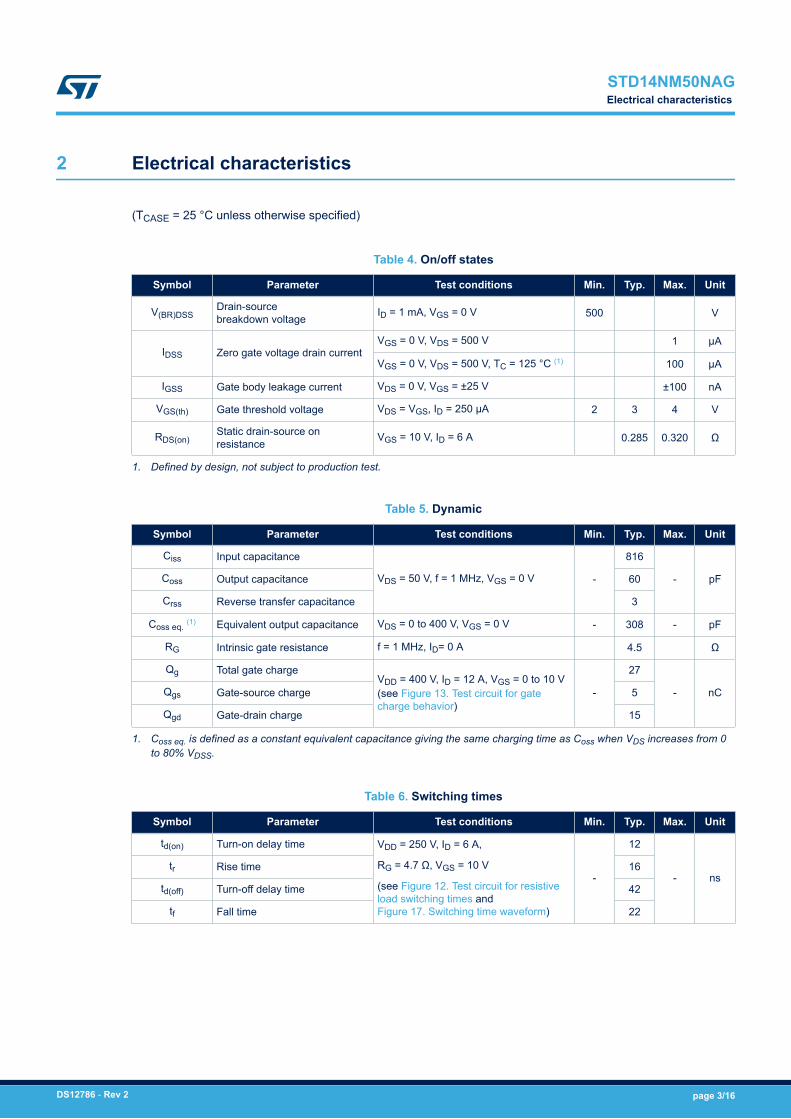
2 Electrical characteristics
(TCASE = 25 °C unless otherwise specified)
Table 4. On/off states
Symbol Parameter Test conditions Min. Typ. Max. Unit
V(BR)DSSDrain-sourcebreakdown voltage ID = 1 mA, VGS = 0 V 500 V
IDSS Zero gate voltage drain currentVGS = 0 V, VDS = 500 V 1 µA
VGS = 0 V, VDS = 500 V, TC = 125 °C (1) 100 µA
IGSS Gate body leakage current VDS = 0 V, VGS = ±25 V ±100 nA
VGS(th) Gate threshold voltage VDS = VGS, ID = 250 µA 2 3 4 V
RDS(on)Static drain-source onresistance VGS = 10 V, ID = 6 A 0.285 0.320 Ω
1. Defined by design, not subject to production test.
Table 5. Dynamic
Symbol Parameter Test conditions Min. Typ. Max. Unit
Ciss Input capacitance
VDS = 50 V, f = 1 MHz, VGS = 0 V -
816
- pFCoss Output capacitance 60
Crss Reverse transfer capacitance 3
Coss eq. (1) Equivalent output capacitance VDS = 0 to 400 V, VGS = 0 V - 308 - pF
RG Intrinsic gate resistance f = 1 MHz, ID= 0 A 4.5 Ω
Qg Total gate chargeVDD = 400 V, ID = 12 A, VGS = 0 to 10 V(see Figure 13. Test circuit for gatecharge behavior)
-
27
- nCQgs Gate-source charge 5
Qgd Gate-drain charge 15
1. Coss eq. is defined as a constant equivalent capacitance giving the same charging time as Coss when VDS increases from 0to 80% VDSS.
Table 6. Switching times
Symbol Parameter Test conditions Min. Typ. Max. Unit
td(on) Turn-on delay time VDD = 250 V, ID = 6 A,
RG = 4.7 Ω, VGS = 10 V
(see Figure 12. Test circuit for resistiveload switching times andFigure 17. Switching time waveform)
-
12
- nstr Rise time 16
td(off) Turn-off delay time 42
tf Fall time 22
STD14NM50NAGElectrical characteristics
DS12786 - Rev 2 page 3/16
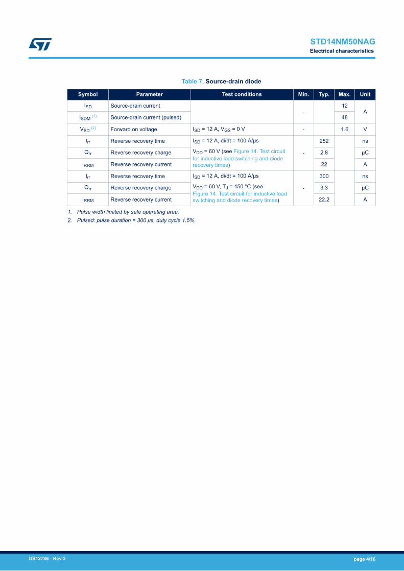
Table 7. Source-drain diode
Symbol Parameter Test conditions Min. Typ. Max. Unit
ISD Source-drain current-
12A
ISDM (1) Source-drain current (pulsed) 48
VSD (2) Forward on voltage ISD = 12 A, VGS = 0 V - 1.6 V
trr Reverse recovery time ISD = 12 A, di/dt = 100 A/µs
VDD = 60 V (see Figure 14. Test circuitfor inductive load switching and dioderecovery times)
-
252 ns
Qrr Reverse recovery charge 2.8 μC
IRRM Reverse recovery current 22 A
trr Reverse recovery time ISD = 12 A, di/dt = 100 A/µs
VDD = 60 V, TJ = 150 °C (seeFigure 14. Test circuit for inductive loadswitching and diode recovery times)
-
300 ns
Qrr Reverse recovery charge 3.3 μC
IRRM Reverse recovery current 22.2 A
1. Pulse width limited by safe operating area.2. Pulsed: pulse duration = 300 μs, duty cycle 1.5%.
STD14NM50NAGElectrical characteristics
DS12786 - Rev 2 page 4/16
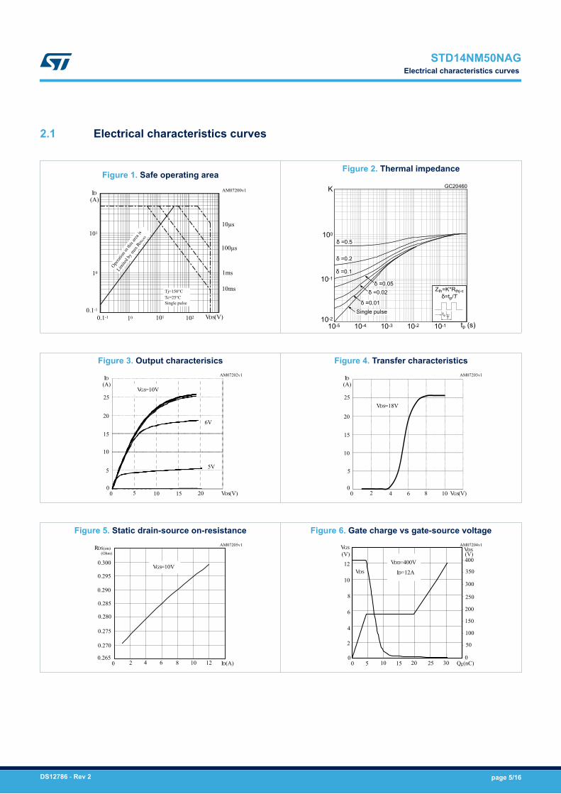
2.1 Electrical characteristics curves
Figure 1. Safe operating area
ID
101
10
0.1-1
VDS(V)
(A)
Operat
ion in
this
area i
s
Limite
d by m
ax RDS(
on)
10µs
100µs
1ms
10msTj=150°CTc=25°CSingle pulse
0.1-1 10 101 102
AM07200v1
Figure 2. Thermal impedance
GC20460
100
10-1
10-2
10-5 10-4 10-3 10-2 10-1
K
tp (s)
Figure 3. Output characterisics
ID
15
10
5
00 10 VDS(V)20
(A)
5 15
20
25
5V
6V
VGS=10V
AM07202v1
Figure 4. Transfer characteristics
ID
15
10
5
00 4 VGS(V)8
(A)
2 6 10
20
25VDS=18V
AM07203v1
Figure 5. Static drain-source on-resistance
RDS(on)
0.280
0.275
0.270
0.2650 4 ID(A)
(Ohm)
2 6
0.285
0.290
0.295
0.300VGS=10V
8 10 12
AM07205v1
Figure 6. Gate charge vs gate-source voltage
VGS
6
4
2
00 5 Qg(nC)
(V)
20
8
10 15
10
VDD=400V
ID=12A
25
12
300
250
200
0
350
400
VDS
30
150
100
50
VDS(V)
AM07204v1
STD14NM50NAGElectrical characteristics curves
DS12786 - Rev 2 page 5/16
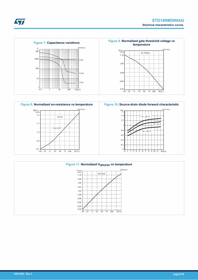
Figure 7. Capacitance variations
C
1000
100
10
10.1 10 VDS(V)
(pF)
1 100
Ciss
Coss
Crss
AM07206v1
Figure 8. Normalized gate threshold voltage vstemperature
VGS(th)
1.00
0.90
0.80
0.70-50 0 TJ(°C)
(norm)
-25
1.10
7525 50 100
ID=250µAAM07208v1
Figure 9. Normalized on-resistance vs temperature
RDS(on)
1.7
1.3
0.9
0.5-50 0 TJ(°C)
(norm)
-25 7525 50 100
2.1ID=6A
VGS=10 V
AM07209v1
Figure 10. Source-drain diode forward characteristic
VSD
0.6
0.4
0.2
00 2 ISD(A)
(V)
1
0.8
53 4 6
TJ= -50 °C
TJ= 150 °C
TJ= 25 °C
7 8 9 10 11
1
1.2
1.4
AM15616v1
Figure 11. Normalized V(BR)DSS vs temperature
V(BR)DSS
-50 0 TJ(°C)
(norm)
-25 7525 50 1000.920.94
0.96
0.98
1.00
1.02
1.04
1.06
ID=1mA
1.08
1.10
AM09028v1
STD14NM50NAGElectrical characteristics curves
DS12786 - Rev 2 page 6/16
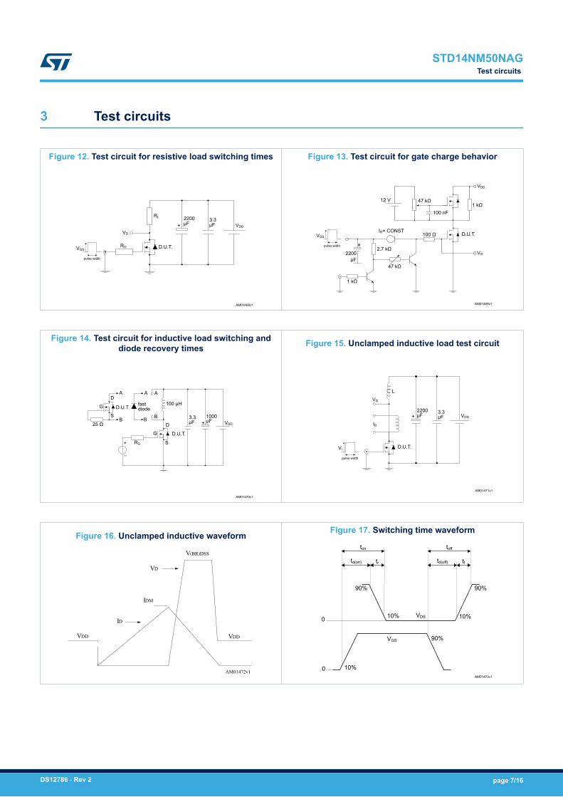
3 Test circuits
Figure 12. Test circuit for resistive load switching times
AM01468v1
VD
RG
RL
D.U.T.
2200μF VDD
3.3μF+
pulse width
VGS
Figure 13. Test circuit for gate charge behavior
AM01469v1
47 kΩ1 kΩ
47 kΩ
2.7 kΩ
1 kΩ
12 V
IG= CONST100 Ω
100 nF
D.U.T.
+pulse width
VGS
2200μF
VG
VDD
Figure 14. Test circuit for inductive load switching anddiode recovery times
AM01470v1
AD
D.U.T.S
B
G
25 Ω
A A
B B
RG
GD
S
100 µH
µF3.3 1000
µF VDD
D.U.T.
+
_
+
fastdiode
Figure 15. Unclamped inductive load test circuit
AM01471v1
VD
ID
D.U.T.
L
VDD+
pulse width
Vi
3.3µF
2200µF
Figure 16. Unclamped inductive waveform
AM01472v1
V(BR)DSS
VDDVDD
VD
IDM
ID
Figure 17. Switching time waveform
AM01473v1
0
VGS 90%
VDS
90%
10%
90%
10%
10%
ton
td(on) tr
0
toff
td(off) tf
STD14NM50NAGTest circuits
DS12786 - Rev 2 page 7/16
4 Package information
In order to meet environmental requirements, ST offers these devices in different grades of ECOPACK®
packages, depending on their level of environmental compliance. ECOPACK® specifications, grade definitionsand product status are available at: www.st.com. ECOPACK® is an ST trademark.
STD14NM50NAGPackage information
DS12786 - Rev 2 page 8/16
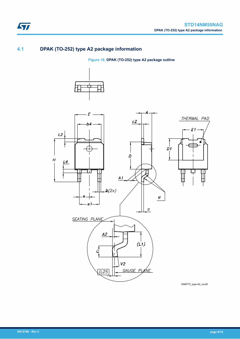
4.1 DPAK (TO-252) type A2 package information
Figure 18. DPAK (TO-252) type A2 package outline
0068772_type-A2_rev26
STD14NM50NAGDPAK (TO-252) type A2 package information
DS12786 - Rev 2 page 9/16
Table 8. DPAK (TO-252) type A2 mechanical data
Dim.mm
Min. Typ. Max.
A 2.20 2.40
A1 0.90 1.10
A2 0.03 0.23
b 0.64 0.90
b4 5.20 5.40
c 0.45 0.60
c2 0.48 0.60
D 6.00 6.20
D1 4.95 5.10 5.25
E 6.40 6.60
E1 5.10 5.20 5.30
e 2.159 2.286 2.413
e1 4.445 4.572 4.699
H 9.35 10.10
L 1.00 1.50
L1 2.60 2.80 3.00
L2 0.65 0.80 0.95
L4 0.60 1.00
R 0.20
V2 0° 8°
STD14NM50NAGDPAK (TO-252) type A2 package information
DS12786 - Rev 2 page 10/16
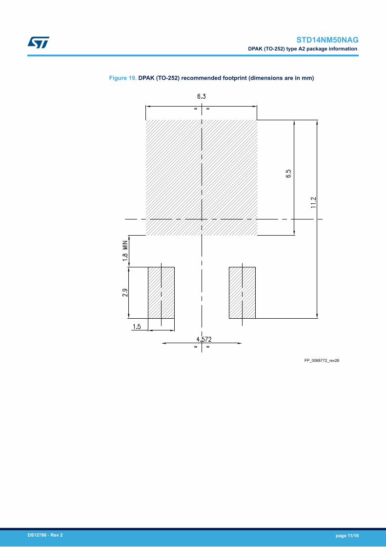
Figure 19. DPAK (TO-252) recommended footprint (dimensions are in mm)
FP_0068772_rev26
STD14NM50NAGDPAK (TO-252) type A2 package information
DS12786 - Rev 2 page 11/16
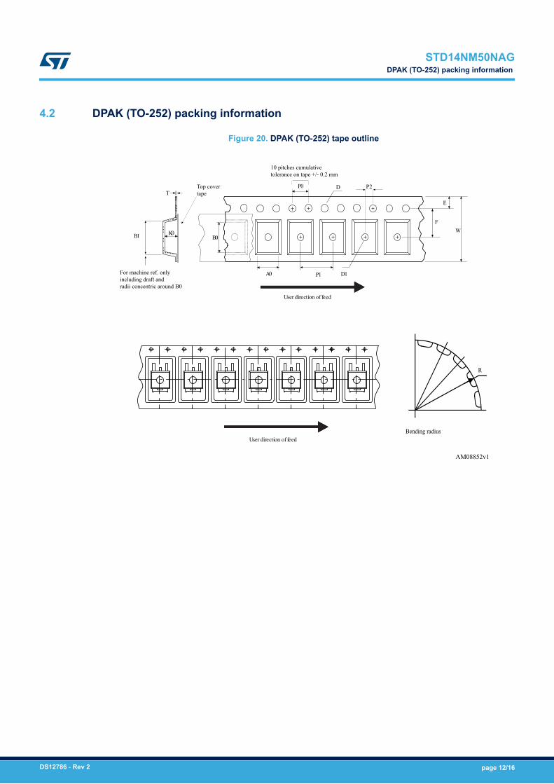
4.2 DPAK (TO-252) packing information
Figure 20. DPAK (TO-252) tape outline
P1A0 D1
P0
FW
E
D
B0K0
T
User direction of feed
P2
10 pitches cumulativetolerance on tape +/- 0.2 mm
User direction of feed
R
Bending radius
B1
For machine ref. onlyincluding draft andradii concentric around B0
AM08852v1
Top covertape
STD14NM50NAGDPAK (TO-252) packing information
DS12786 - Rev 2 page 12/16
Figure 21. DPAK (TO-252) reel outline
A
D
B
Full radius
Tape slot in core for tape start
2.5mm min.width
G measured at hub
C
N
40mm min. access hole at slot location
T
AM06038v1
Table 9. DPAK (TO-252) tape and reel mechanical data
Tape Reel
Dim.mm
Dim.mm
Min. Max. Min. Max.
A0 6.8 7 A 330
B0 10.4 10.6 B 1.5
B1 12.1 C 12.8 13.2
D 1.5 1.6 D 20.2
D1 1.5 G 16.4 18.4
E 1.65 1.85 N 50
F 7.4 7.6 T 22.4
K0 2.55 2.75
P0 3.9 4.1 Base qty. 2500
P1 7.9 8.1 Bulk qty. 2500
P2 1.9 2.1
R 40
T 0.25 0.35
W 15.7 16.3
STD14NM50NAGDPAK (TO-252) packing information
DS12786 - Rev 2 page 13/16
Revision history
Table 10. Document revision history
Date Version Changes
15-Oct-2018 1 Initial release. The document status is production data.
04-Mar-2019 2 Updated Section Device summary.
STD14NM50NAG
DS12786 - Rev 2 page 14/16
Contents
1 Electrical ratings . . . . . . . . . . . . . . . . . . . . . . . . . . . . . . . . . . . . . . . . . . . . . . . . . . . . . . . . . . . . . . . . . .2
2 Electrical characteristics. . . . . . . . . . . . . . . . . . . . . . . . . . . . . . . . . . . . . . . . . . . . . . . . . . . . . . . . . . .3
2.1 Electrical characteristics curves . . . . . . . . . . . . . . . . . . . . . . . . . . . . . . . . . . . . . . . . . . . . . . . . . . 5
3 Test circuits . . . . . . . . . . . . . . . . . . . . . . . . . . . . . . . . . . . . . . . . . . . . . . . . . . . . . . . . . . . . . . . . . . . . . . .7
4 Package information. . . . . . . . . . . . . . . . . . . . . . . . . . . . . . . . . . . . . . . . . . . . . . . . . . . . . . . . . . . . . . .8
4.1 DPAK (TO-252) type A2 package information . . . . . . . . . . . . . . . . . . . . . . . . . . . . . . . . . . . . . . . 8
4.2 DPAK (TO-252) packing information. . . . . . . . . . . . . . . . . . . . . . . . . . . . . . . . . . . . . . . . . . . . . . 11
Revision history . . . . . . . . . . . . . . . . . . . . . . . . . . . . . . . . . . . . . . . . . . . . . . . . . . . . . . . . . . . . . . . . . . . . . . .14
STD14NM50NAGContents
DS12786 - Rev 2 page 15/16
IMPORTANT NOTICE – PLEASE READ CAREFULLY
STMicroelectronics NV and its subsidiaries (“ST”) reserve the right to make changes, corrections, enhancements, modifications, and improvements to STproducts and/or to this document at any time without notice. Purchasers should obtain the latest relevant information on ST products before placing orders. STproducts are sold pursuant to ST’s terms and conditions of sale in place at the time of order acknowledgement.
Purchasers are solely responsible for the choice, selection, and use of ST products and ST assumes no liability for application assistance or the design ofPurchasers’ products.
No license, express or implied, to any intellectual property right is granted by ST herein.
Resale of ST products with provisions different from the information set forth herein shall void any warranty granted by ST for such product.
ST and the ST logo are trademarks of ST. All other product or service names are the property of their respective owners.
Information in this document supersedes and replaces information previously supplied in any prior versions of this document.
© 2019 STMicroelectronics – All rights reserved
STD14NM50NAG
DS12786 - Rev 2 page 16/16