N-channel 650 V, 0.075 typ., 22.5 A MDmesh M5 Power … · 5 Revision history ... D D.U.T. S B G A...
16
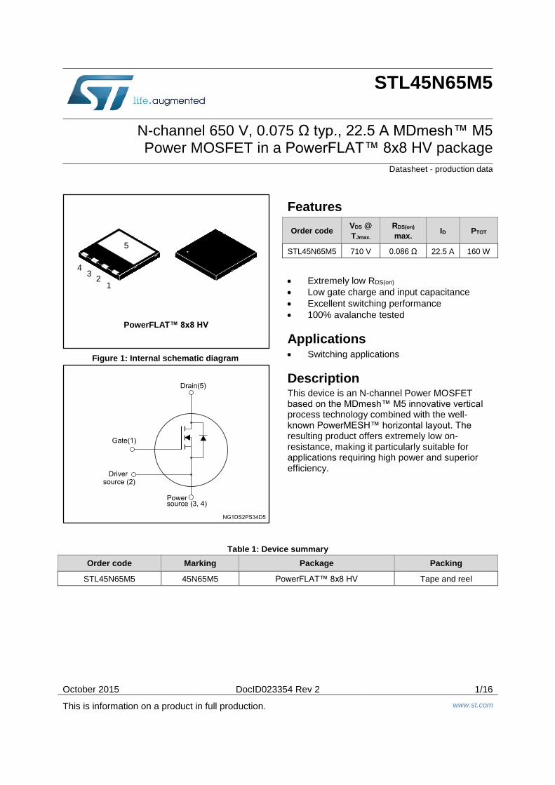
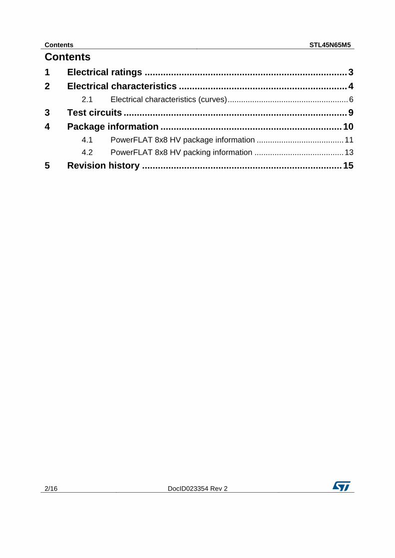
October 2015 DocID023354 Rev 2 1/16 This is information on a product in full production. www.st.com STL45N65M5 N-channel 650 V, 0.075 Ω typ., 22.5 A MDmesh™ M5 Power MOSFET in a PowerFLAT™ 8x8 HV package Datasheet - production data Figure 1: Internal schematic diagram Features Order code VDS @ TJmax. RDS(on) max. ID PTOT STL45N65M5 710 V 0.086 Ω 22.5 A 160 W Extremely low RDS(on) Low gate charge and input capacitance Excellent switching performance 100% avalanche tested Applications Switching applications Description This device is an N-channel Power MOSFET based on the MDmesh™ M5 innovative vertical process technology combined with the well- known PowerMESH™ horizontal layout. The resulting product offers extremely low on- resistance, making it particularly suitable for applications requiring high power and superior efficiency. Table 1: Device summary Order code Marking Package Packing STL45N65M5 45N65M5 PowerFLAT™ 8x8 HV Tape and reel 5 1 2 3 4 PowerFLAT™ 8x8 HV
Transcript of N-channel 650 V, 0.075 typ., 22.5 A MDmesh M5 Power … · 5 Revision history ... D D.U.T. S B G A...
October 2015 DocID023354 Rev 2 1/16
This is information on a product in full production. www.st.com
STL45N65M5
N-channel 650 V, 0.075 Ω typ., 22.5 A MDmesh™ M5 Power MOSFET in a PowerFLAT™ 8x8 HV package
Datasheet - production data
Figure 1: Internal schematic diagram
Features
Order code VDS @
TJmax.
RDS(on)
max. ID PTOT
STL45N65M5 710 V 0.086 Ω 22.5 A 160 W
Extremely low RDS(on)
Low gate charge and input capacitance
Excellent switching performance
100% avalanche tested
Applications Switching applications
Description This device is an N-channel Power MOSFET based on the MDmesh™ M5 innovative vertical process technology combined with the well-known PowerMESH™ horizontal layout. The resulting product offers extremely low on-resistance, making it particularly suitable for applications requiring high power and superior efficiency.
Table 1: Device summary
Order code Marking Package Packing
STL45N65M5 45N65M5 PowerFLAT™ 8x8 HV Tape and reel
5
12
34
PowerFLAT™ 8x8 HV
Contents STL45N65M5
2/16 DocID023354 Rev 2
Contents
1 Electrical ratings ............................................................................. 3
2 Electrical characteristics ................................................................ 4
2.1 Electrical characteristics (curves) ...................................................... 6
3 Test circuits ..................................................................................... 9
4 Package information ..................................................................... 10
4.1 PowerFLAT 8x8 HV package information ....................................... 11
4.2 PowerFLAT 8x8 HV packing information ........................................ 13
5 Revision history ............................................................................ 15
STL45N65M5 Electrical ratings
DocID023354 Rev 2 3/16
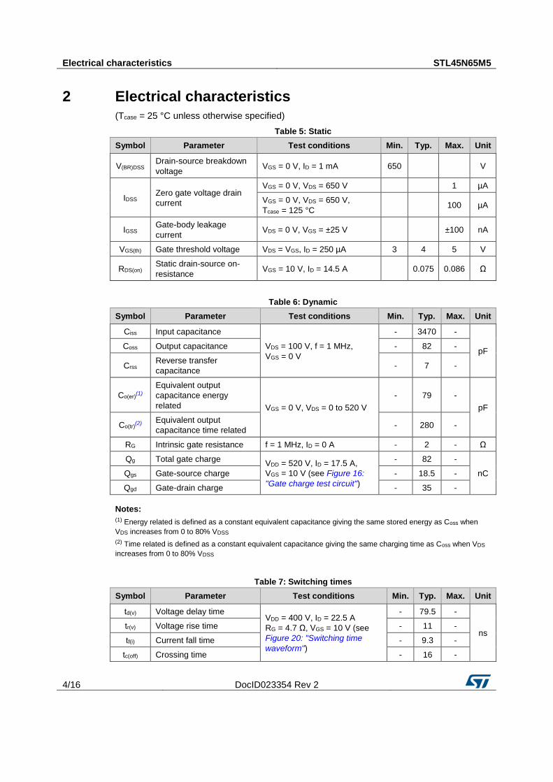
1 Electrical ratings Table 2: Absolute maximum ratings
Symbol Parameter Value Unit
VDS Drain-source voltage 650 V
VGS Gate-source voltage ±25 V
ID(1) Drain current (continuous) at Tcase = 25 °C 22.5
A Drain current (continuous) at Tcase = 100 °C 18
IDM(1)(2) Drain current (pulsed) 90 A
PTOT(1) Total dissipation at Tcase = 25 °C 160 W
ID(3) Drain current (continuous) at Tamb = 25 °C 3.8
A Drain current (continuous) at Tamb = 100 °C 2.4
PTOT(3) Total dissipation at Tamb = 25 °C 2.8 W
dv/dt(4) Peak diode recovery voltage slope 15 V/ns
Tstg Storage temperature -55 to 150 °C
Tj Operating junction temperature
Notes:
(1) The value is rated according to Rthj-case and limited by package. (2) Pulse width limited by safe operating area. (3) When mounted on a 1-inch² FR-4, 2oz Cu board. (4) ISD ≤ 22.5 A, di/dt ≤ 400 A/μs, VDD = 400 V, VDS(peak) < V(BR)DSS.
Table 3: Thermal data
Symbol Parameter Value Unit
Rthj-case Thermal resistance junction-case 0.78 °C/W
Rthj-amb(1) Thermal resistance junction-ambient 45
Notes:
(1) When mounted on a 1-inch² FR-4, 2oz Cu board.
Table 4: Avalanche characteristics
Symbol Parameter Value Unit
IAR(1) Avalanche current, repetitive or not repetitive 8 A
EAS(2) Single pulse avalanche energy 810 mJ
Notes:
(1) Pulse width limited by Tjmax. (2) starting Tj = 25 °C, ID = IAR, VDD = 50 V.
Electrical characteristics STL45N65M5
4/16 DocID023354 Rev 2
2 Electrical characteristics
(Tcase = 25 °C unless otherwise specified)
Table 5: Static
Symbol Parameter Test conditions Min. Typ. Max. Unit
V(BR)DSS Drain-source breakdown
voltage VGS = 0 V, ID = 1 mA 650
V
IDSS Zero gate voltage drain
current
VGS = 0 V, VDS = 650 V
1 µA
VGS = 0 V, VDS = 650 V,
Tcase = 125 °C 100 µA
IGSS Gate-body leakage
current VDS = 0 V, VGS = ±25 V
±100 nA
VGS(th) Gate threshold voltage VDS = VGS, ID = 250 µA 3 4 5 V
RDS(on) Static drain-source on-
resistance VGS = 10 V, ID = 14.5 A
0.075 0.086 Ω
Table 6: Dynamic
Symbol Parameter Test conditions Min. Typ. Max. Unit
Ciss Input capacitance
VDS = 100 V, f = 1 MHz,
VGS = 0 V
- 3470 -
pF Coss Output capacitance - 82 -
Crss Reverse transfer
capacitance - 7 -
Co(er)(1)
Equivalent output
capacitance energy
related VGS = 0 V, VDS = 0 to 520 V
- 79 -
pF
Co(tr)(2)
Equivalent output
capacitance time related - 280 -
RG Intrinsic gate resistance f = 1 MHz, ID = 0 A - 2 - Ω
Qg Total gate charge VDD = 520 V, ID = 17.5 A,
VGS = 10 V (see Figure 16:
"Gate charge test circuit")
- 82 -
nC Qgs Gate-source charge - 18.5 -
Qgd Gate-drain charge - 35 -
Notes:
(1) Energy related is defined as a constant equivalent capacitance giving the same stored energy as Coss when
VDS increases from 0 to 80% VDSS (2) Time related is defined as a constant equivalent capacitance giving the same charging time as Coss when VDS
increases from 0 to 80% VDSS
Table 7: Switching times
Symbol Parameter Test conditions Min. Typ. Max. Unit
td(v) Voltage delay time VDD = 400 V, ID = 22.5 A
RG = 4.7 Ω, VGS = 10 V (see
Figure 20: "Switching time
waveform")
- 79.5 -
ns tr(v) Voltage rise time - 11 -
tf(i) Current fall time - 9.3 -
tc(off) Crossing time - 16 -
STL45N65M5 Electrical characteristics
DocID023354 Rev 2 5/16
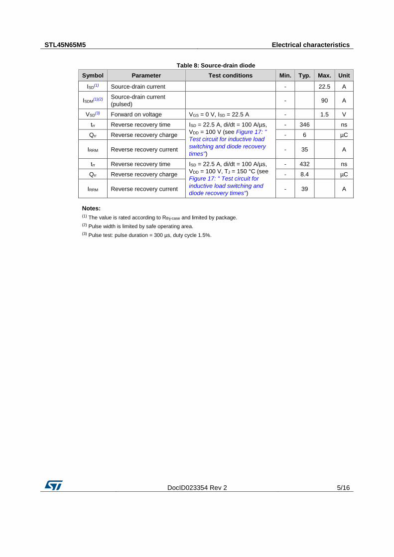
Table 8: Source-drain diode
Symbol Parameter Test conditions Min. Typ. Max. Unit
ISD(1) Source-drain current
-
22.5 A
ISDM(1)(2)
Source-drain current
(pulsed) -
90 A
VSD(3) Forward on voltage VGS = 0 V, ISD = 22.5 A -
1.5 V
trr Reverse recovery time ISD = 22.5 A, di/dt = 100 A/µs,
VDD = 100 V (see Figure 17: "
Test circuit for inductive load
switching and diode recovery
times")
- 346
ns
Qrr Reverse recovery charge - 6
µC
IRRM Reverse recovery current - 35
A
trr Reverse recovery time ISD = 22.5 A, di/dt = 100 A/µs,
VDD = 100 V, TJ = 150 °C (see
Figure 17: " Test circuit for
inductive load switching and
diode recovery times")
- 432
ns
Qrr Reverse recovery charge - 8.4
µC
IRRM Reverse recovery current - 39
A
Notes:
(1) The value is rated according to Rthj-case and limited by package. (2) Pulse width is limited by safe operating area. (3) Pulse test: pulse duration = 300 µs, duty cycle 1.5%.
Electrical characteristics STL45N65M5
6/16 DocID023354 Rev 2
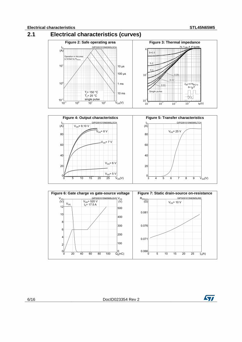
2.1 Electrical characteristics (curves)
Figure 2: Safe operating area
Figure 3: Thermal impedance
Figure 4: Output characteristics
Figure 5: Transfer characteristics
Figure 6: Gate charge vs gate-source voltage
Figure 7: Static drain-source on-resistance
10-5
10-4
10-3
10-2
tp(s)10
-2
10-1
K
0.2
0.05
0.02
0.01
0.1
Single pulse
δ=0.5
Zth= K*RthJ-cδ= tp/Ƭ
tpƬ
STL45N65M5 Electrical characteristics
DocID023354 Rev 2 7/16
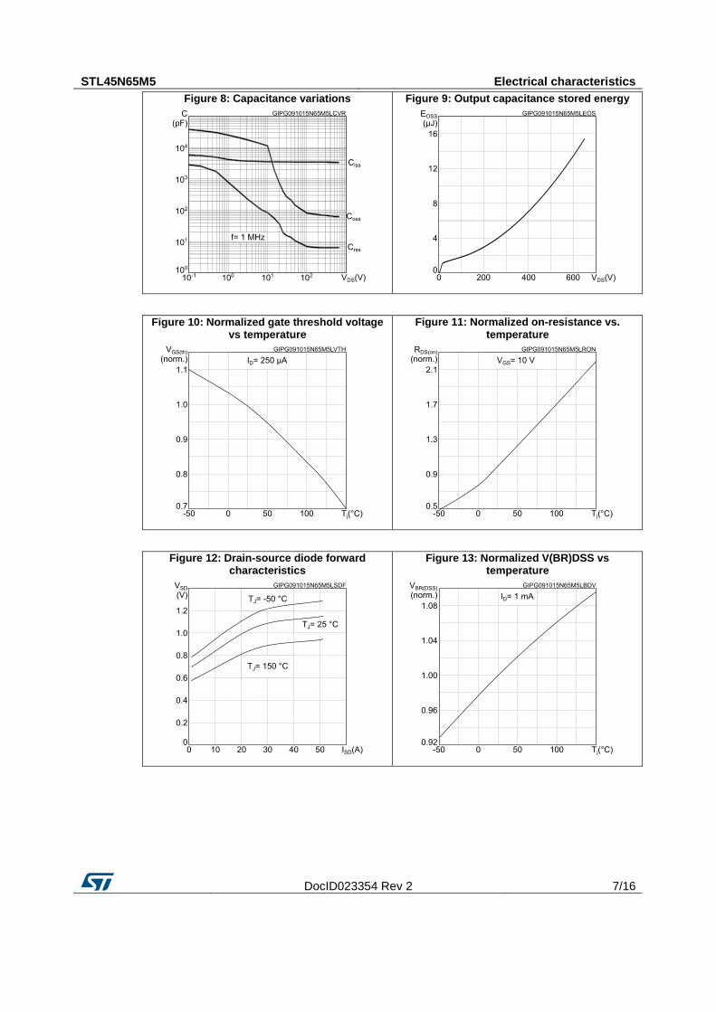
Figure 8: Capacitance variations
Figure 9: Output capacitance stored energy
Figure 10: Normalized gate threshold voltage vs temperature
Figure 11: Normalized on-resistance vs. temperature
Figure 12: Drain-source diode forward characteristics
Figure 13: Normalized V(BR)DSS vs temperature
Electrical characteristics STL45N65M5
8/16 DocID023354 Rev 2
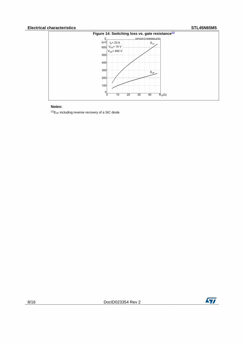
Figure 14: Switching loss vs. gate resistance(1)
Notes:
(1)Eon including reverse recovery of a SiC diode
STL45N65M5 Test circuits
DocID023354 Rev 2 9/16
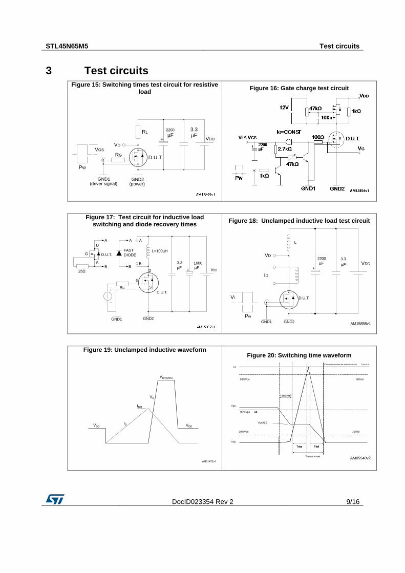
3 Test circuits Figure 15: Switching times test circuit for resistive
load
Figure 16: Gate charge test circuit
Figure 17: Test circuit for inductive load switching and diode recovery times
Figure 18: Unclamped inductive load test circuit
Figure 19: Unclamped inductive waveform
Figure 20: Switching time waveform
VGS
PW
VD
RG
RL
D.U.T.
2200
µF3.3µF
VDD
GND2(power)
GND1(driver signal)
+
A
D
D.U.T.
SB
G
25Ω
A A
BB
RG
G
FAST
DIODE
D
S
L=100µH
µF
3.3 1000µF
VDD
GND1 GND2
D.U.T.
+
AM15858v1
Vi
Pw
VD
ID
D.U.T.
L
2200
µF3.3
µF VDD
GND1 GND2
+
AM05540v2
Id
Vgs
Vds
90%Vds
10%Id
90%Vgs on
Tdelay-off
TfallTrise
Tcross -over
10%Vds
90%Id
Vgs(I(t))
on
-off
TfallTrise
-
))
Concept waveform for Inductive Load Turn-o ff
Package information STL45N65M5
10/16 DocID023354 Rev 2
4 Package information
In order to meet environmental requirements, ST offers these devices in different grades of ECOPACK® packages, depending on their level of environmental compliance. ECOPACK® specifications, grade definitions and product status are available at: www.st.com. ECOPACK® is an ST trademark.
STL45N65M5 Package information
DocID023354 Rev 2 11/16
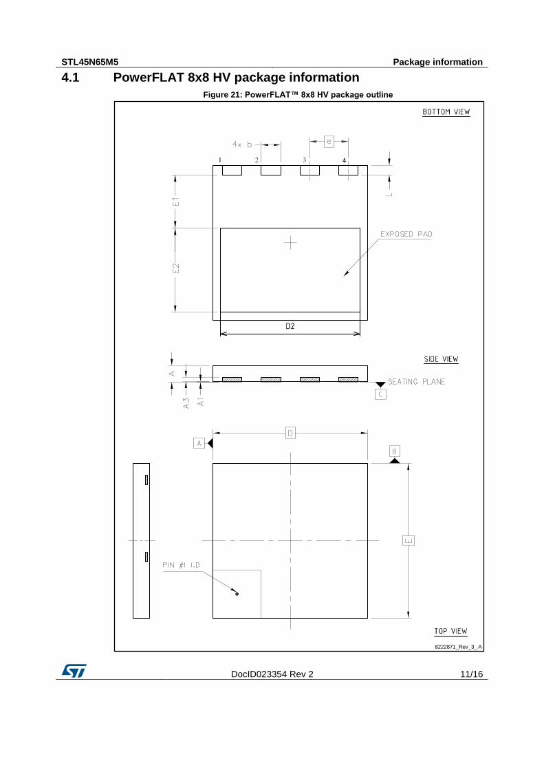
4.1 PowerFLAT 8x8 HV package information
Figure 21: PowerFLAT™ 8x8 HV package outline
8222871_Rev_3_ A
Package information STL45N65M5
12/16 DocID023354 Rev 2
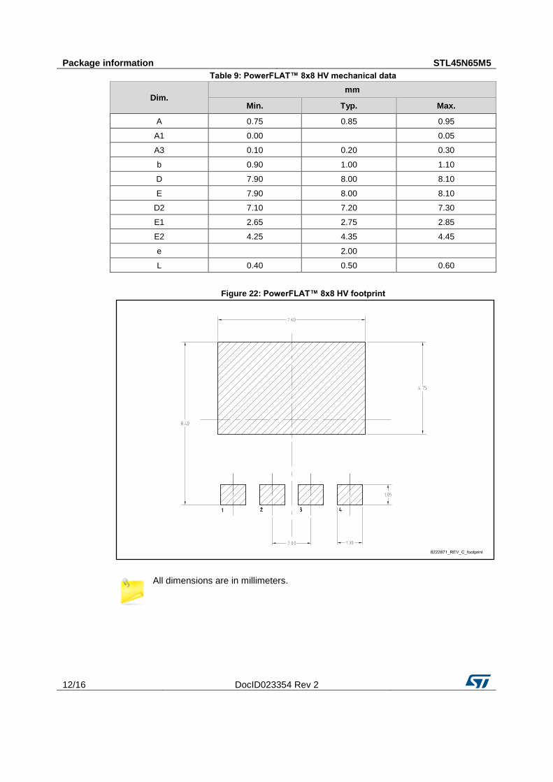
Table 9: PowerFLAT™ 8x8 HV mechanical data
Dim. mm
Min. Typ. Max.
A 0.75 0.85 0.95
A1 0.00
0.05
A3 0.10 0.20 0.30
b 0.90 1.00 1.10
D 7.90 8.00 8.10
E 7.90 8.00 8.10
D2 7.10 7.20 7.30
E1 2.65 2.75 2.85
E2 4.25 4.35 4.45
e
2.00
L 0.40 0.50 0.60
Figure 22: PowerFLAT™ 8x8 HV footprint
All dimensions are in millimeters.
STL45N65M5 Package information
DocID023354 Rev 2 13/16
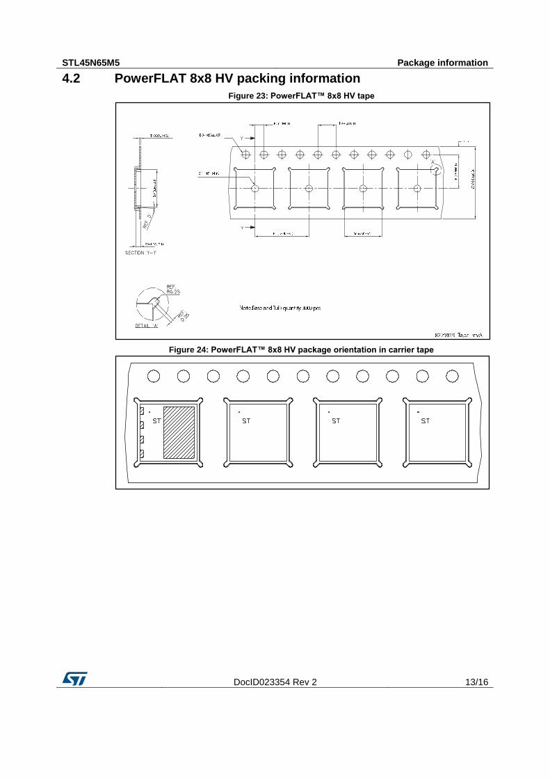
4.2 PowerFLAT 8x8 HV packing information
Figure 23: PowerFLAT™ 8x8 HV tape
Figure 24: PowerFLAT™ 8x8 HV package orientation in carrier tape
Package information STL45N65M5
14/16 DocID023354 Rev 2
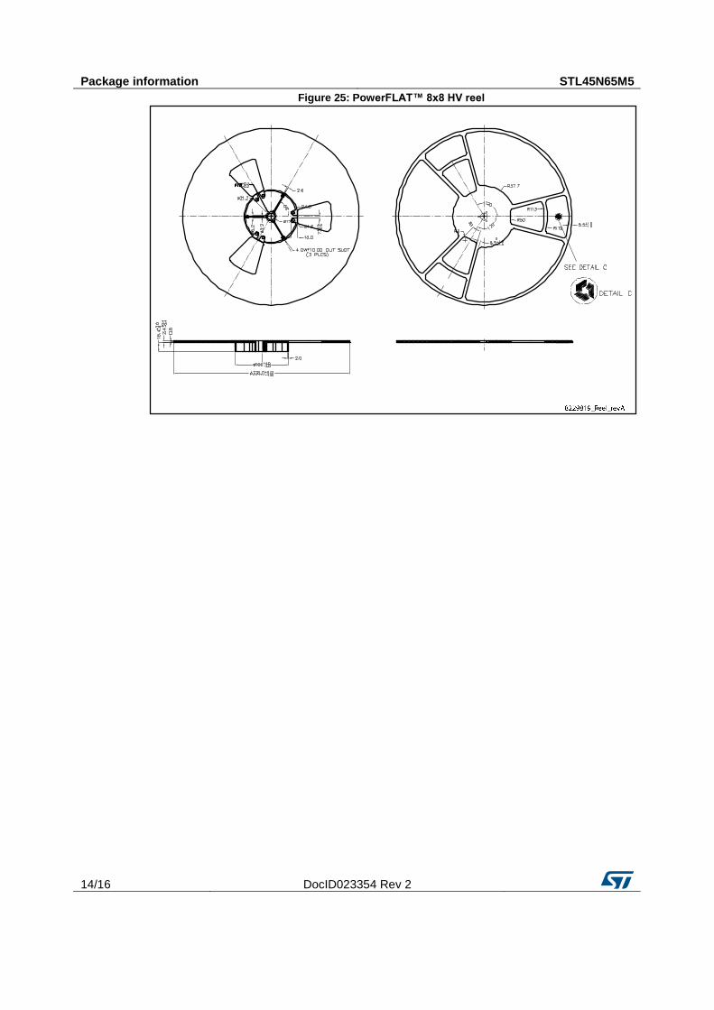
Figure 25: PowerFLAT™ 8x8 HV reel
STL45N65M5 Revision history
DocID023354 Rev 2 15/16
5 Revision history Table 10: Document revision history
Date Revision Changes
20-Sep-2012 1 First release.
09-Oct-2015 2
Text and formatting changes throughout document
Datasheet status changed from preliminary to production data
In section Electrical ratings:
- added table Avalanche characteristics
In section Electrical characteristics:
- renamed table Static (was On /off states)
Updated section Test circuits
Updated and renamed section Package information (was Package
mechanical data)
STL45N65M5
16/16 DocID023354 Rev 2
IMPORTANT NOTICE – PLEASE READ CAREFULLY
STMicroelectronics NV and its subsidiaries (“ST”) reserve the right to make changes, corrections, enhancements, modifications, and improvements to ST products and/or to this document at any time without notice. Purchasers should obtain the latest relevant information on ST products before placing orders. ST products are sold pursuant to ST’s terms and conditions of sale in place at the time of order acknowledgement.
Purchasers are solely responsible for the choice, selection, and use of ST products and ST assumes no liability for application assistance or the design of Purchasers’ products.
No license, express or implied, to any intellectual property right is granted by ST herein.
Resale of ST products with provisions different from the information set forth herein shall void any warranty granted by ST for such product.
ST and the ST logo are trademarks of ST. All other product or service names are the property of their respective owners.
Information in this document supersedes and replaces information previously supplied in any prior versions of this document.
© 2015 STMicroelectronics – All rights reserved