CSD18533Q5A 60 V N-Channel NexFET™ Power · PDF fileCSD18533Q5A 60 V N-Channel...
13
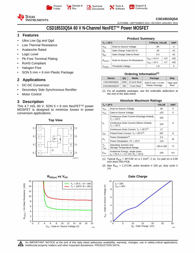
0 2 4 6 8 10 12 14 16 0 2 4 6 8 10 12 14 16 18 20 V GS - Gate-to- Source Voltage (V) R DS(on29 - On-State Resistance (mΩ) T C = 25°C Id = 18A T C = 125ºC Id = 18A G001 0 2 4 6 8 10 0 5 10 15 20 25 30 Q g - Gate Charge (nC) V GS - Gate-to-Source Voltage (V) I D = 18A V DS = 30V G001 1 D 2 D 3 D 4 D D 5 G 6 S 7 S 8 S P0093-01 Product Folder Sample & Buy Technical Documents Tools & Software Support & Community CSD18533Q5A SLPS388B – SEPTEMBER 2012 – REVISED JANUARY 2015 CSD18533Q5A 60 V N-Channel NexFET™ Power MOSFET 1 Features Product Summary 1• Ultra Low Qg and Qgd T A = 25°C TYPICAL VALUE UNIT • Low Thermal Resistance V DS Drain-to-Source Voltage 60 V • Avalanche Rated Q g Gate Charge Total (10 V) 29 nC Q gd Gate Charge Gate-to-Drain 5.4 nC • Logic Level V GS = 4.5 V 6.5 mΩ • Pb Free Terminal Plating R DS(on) Drain-to-Source On-Resistance V GS = 10 V 4.7 mΩ • RoHS Compliant V GS(th) Threshold Voltage 1.9 V • Halogen Free • SON 5 mm × 6 mm Plastic Package . Ordering Information (1) Device Qty Media Package Ship 2 Applications CSD18533Q5A 2500 13-Inch Reel SON 5 mm × 6 mm Tape and Plastic Package Reel • DC-DC Conversion CSD18533Q5AT 250 7-Inch Reel • Secondary Side Synchronous Rectifier (1) For all available packages, see the orderable addendum at the end of the data sheet. • Motor Control Absolute Maximum Ratings 3 Description T A = 25°C VALUE UNIT This 4.7 mΩ, 60 V, SON 5 × 6 mm NexFET™ power V DS Drain-to-Source Voltage 60 V MOSFET is designed to minimize losses in power V GS Gate-to-Source Voltage ±20 V conversion applications. Continuous Drain Current (Package limited), 100 T C = 25°C Top View I D Continuous Drain Current (Silicon limited), A 103 T C = 25°C Continuous Drain Current, T A = 25°C (1) 17 I DM Pulsed Drain Current, T A = 25°C (2) 267 A Power Dissipation (1) 3.2 P D W Power Dissipation, TC = 25°C 116 T J , Operating Junction and –55 to 150 °C T stg Storage Temperature Range Avalanche Energy, single pulse E AS 140 mJ I D = 53 A, L = 0.1 mH, R G = 25 Ω (1) Typical R θJA = 40°C/W on a 1 inch 2 , 2 oz. Cu pad on a 0.06 inch thick FR4 PCB. (2) Max R θJC = 1.3°C/W, pulse duration ≤ 100 μs, duty cycle ≤ 1% R DS(on) vs V GS Gate Charge 1 An IMPORTANT NOTICE at the end of this data sheet addresses availability, warranty, changes, use in safety-critical applications, intellectual property matters and other important disclaimers. PRODUCTION DATA.
Transcript of CSD18533Q5A 60 V N-Channel NexFET™ Power · PDF fileCSD18533Q5A 60 V N-Channel...
0
2
4
6
8
10
12
14
16
0 2 4 6 8 10 12 14 16 18 20VGS - Gate-to- Source Voltage (V)
RD
S(o
n) -
On-
Sta
te R
esis
tanc
e (
mΩ
) TC = 25°C Id = 18ATC = 125ºC Id = 18A
G001
0
2
4
6
8
10
0 5 10 15 20 25 30Qg - Gate Charge (nC)
VG
S -
Gat
e-to
-Sou
rce
Vol
tage
(V
) ID = 18AVDS = 30V
G001
1 D
2 D
3 D
4
D
D5G
6S
7S
8S
P0093-01
Product
Folder
Sample &Buy
Technical
Documents
Tools &
Software
Support &Community
CSD18533Q5ASLPS388B –SEPTEMBER 2012–REVISED JANUARY 2015
CSD18533Q5A 60 V N-Channel NexFET™ Power MOSFET1 Features
Product Summary1• Ultra Low Qg and Qgd
TA = 25°C TYPICAL VALUE UNIT• Low Thermal Resistance VDS Drain-to-Source Voltage 60 V• Avalanche Rated Qg Gate Charge Total (10 V) 29 nC
Qgd Gate Charge Gate-to-Drain 5.4 nC• Logic LevelVGS = 4.5 V 6.5 mΩ• Pb Free Terminal Plating RDS(on) Drain-to-Source On-ResistanceVGS = 10 V 4.7 mΩ• RoHS Compliant
VGS(th) Threshold Voltage 1.9 V• Halogen Free• SON 5 mm × 6 mm Plastic Package . Ordering Information(1)
Device Qty Media Package Ship2 ApplicationsCSD18533Q5A 2500 13-Inch Reel SON 5 mm × 6 mm Tape and
Plastic Package Reel• DC-DC Conversion CSD18533Q5AT 250 7-Inch Reel
• Secondary Side Synchronous Rectifier (1) For all available packages, see the orderable addendum atthe end of the data sheet.• Motor Control
Absolute Maximum Ratings3 DescriptionTA = 25°C VALUE UNITThis 4.7 mΩ, 60 V, SON 5 × 6 mm NexFET™ powerVDS Drain-to-Source Voltage 60 VMOSFET is designed to minimize losses in powerVGS Gate-to-Source Voltage ±20 Vconversion applications.
Continuous Drain Current (Package limited), 100TC = 25°CTop ViewID Continuous Drain Current (Silicon limited), A103TC = 25°C
Continuous Drain Current, TA = 25°C(1) 17
IDM Pulsed Drain Current, TA = 25°C(2) 267 A
Power Dissipation(1) 3.2PD W
Power Dissipation, TC = 25°C 116
TJ, Operating Junction and –55 to 150 °CTstg Storage Temperature Range
Avalanche Energy, single pulseEAS 140 mJID = 53 A, L = 0.1 mH, RG = 25 Ω
(1) Typical RθJA = 40°C/W on a 1 inch2, 2 oz. Cu pad on a 0.06inch thick FR4 PCB.
(2) Max RθJC = 1.3°C/W, pulse duration ≤ 100 μs, duty cycle ≤1%
RDS(on) vs VGS Gate Charge
1
An IMPORTANT NOTICE at the end of this data sheet addresses availability, warranty, changes, use in safety-critical applications,intellectual property matters and other important disclaimers. PRODUCTION DATA.
CSD18533Q5ASLPS388B –SEPTEMBER 2012–REVISED JANUARY 2015 www.ti.com
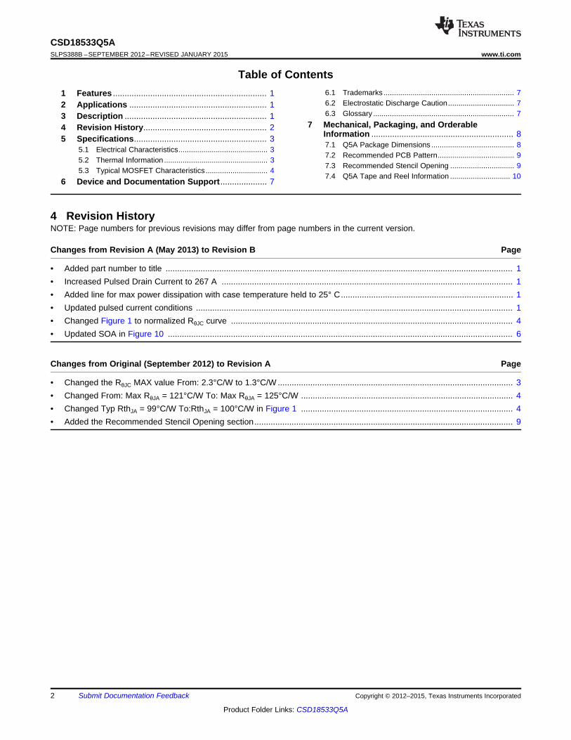
Table of Contents6.1 Trademarks ............................................................... 71 Features .................................................................. 16.2 Electrostatic Discharge Caution................................ 72 Applications ........................................................... 16.3 Glossary .................................................................... 73 Description ............................................................. 1
7 Mechanical, Packaging, and Orderable4 Revision History..................................................... 2Information ............................................................. 85 Specifications......................................................... 37.1 Q5A Package Dimensions ........................................ 85.1 Electrical Characteristics........................................... 37.2 Recommended PCB Pattern..................................... 95.2 Thermal Information .................................................. 37.3 Recommended Stencil Opening ............................... 95.3 Typical MOSFET Characteristics.............................. 47.4 Q5A Tape and Reel Information ............................. 106 Device and Documentation Support.................... 7
4 Revision HistoryNOTE: Page numbers for previous revisions may differ from page numbers in the current version.
Changes from Revision A (May 2013) to Revision B Page
• Added part number to title ..................................................................................................................................................... 1• Increased Pulsed Drain Current to 267 A ............................................................................................................................. 1• Added line for max power dissipation with case temperature held to 25° C.......................................................................... 1• Updated pulsed current conditions ........................................................................................................................................ 1• Changed Figure 1 to normalized RθJC curve ......................................................................................................................... 4• Updated SOA in Figure 10 .................................................................................................................................................... 6
Changes from Original (September 2012) to Revision A Page
• Changed the RθJC MAX value From: 2.3°C/W to 1.3°C/W ..................................................................................................... 3• Changed From: Max RθJA = 121°C/W To: Max RθJA = 125°C/W ........................................................................................... 4• Changed Typ RthJA = 99°C/W To:RthJA = 100°C/W in Figure 1 ........................................................................................... 4• Added the Recommended Stencil Opening section............................................................................................................... 9
2 Submit Documentation Feedback Copyright © 2012–2015, Texas Instruments Incorporated
Product Folder Links: CSD18533Q5A
CSD18533Q5Awww.ti.com SLPS388B –SEPTEMBER 2012–REVISED JANUARY 2015
5 Specifications
5.1 Electrical Characteristics(TA = 25°C unless otherwise stated)
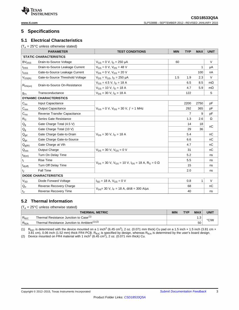
PARAMETER TEST CONDITIONS MIN TYP MAX UNIT¨STATIC CHARACTERISTICSBVDSS Drain-to-Source Voltage VGS = 0 V, ID = 250 μA 60 VIDSS Drain-to-Source Leakage Current VGS = 0 V, VDS = 48 V 1 μAIGSS Gate-to-Source Leakage Current VDS = 0 V, VGS = 20 V 100 nAVGS(th) Gate-to-Source Threshold Voltage VDS = VGS, ID = 250 μA 1.5 1.9 2.3 V
VGS = 4.5 V, ID = 18 A 6.5 8.5 mΩRDS(on) Drain-to-Source On-Resistance
VGS = 10 V, ID = 18 A 4.7 5.9 mΩgƒs Transconductance VDS = 30 V, ID = 18 A 122 SDYNAMIC CHARACTERISTICSCiss Input Capacitance 2200 2750 pFCoss Output Capacitance VGS = 0 V, VDS = 30 V, ƒ = 1 MHz 292 365 pFCrss Reverse Transfer Capacitance 7 9 pFRG Series Gate Resistance 1.3 2.6 ΩQg Gate Charge Total (4.5 V) 14 18
nCQg Gate Charge Total (10 V) 29 36Qgd Gate Charge Gate-to-Drain VDS = 30 V, ID = 18 A 5.4 nCQgs Gate Charge Gate-to-Source 6.6 nCQg(th) Gate Charge at Vth 4.7 nCQoss Output Charge VDS = 30 V, VGS = 0 V 31 nCtd(on) Turn On Delay Time 5.2 nstr Rise Time 5.5 ns
VDS = 30 V, VGS = 10 V, IDS = 18 A, RG = 0 Ωtd(off) Turn Off Delay Time 15 nstƒ Fall Time 2.0 nsDIODE CHARACTERISTICSVSD Diode Forward Voltage ISD = 18 A, VGS = 0 V 0.8 1 VQrr Reverse Recovery Charge 68 nC
VDS= 30 V, IF = 18 A, di/dt = 300 A/μstrr Reverse Recovery Time 40 ns
5.2 Thermal Information(TA = 25°C unless otherwise stated)
THERMAL METRIC MIN TYP MAX UNITRθJC Thermal Resistance Junction to Case (1) 1.3
°C/WRθJA Thermal Resistance Junction to Ambient (1) (2) 50
(1) RθJC is determined with the device mounted on a 1 inch2 (6.45 cm2), 2 oz. (0.071 mm thick) Cu pad on a 1.5 inch × 1.5 inch (3.81 cm ×3.81 cm), 0.06 inch (1.52 mm) thick FR4 PCB. RθJC is specified by design, whereas RθJA is determined by the user’s board design.
(2) Device mounted on FR4 material with 1 inch2 (6.45 cm2), 2 oz. (0.071 mm thick) Cu.
Copyright © 2012–2015, Texas Instruments Incorporated Submit Documentation Feedback 3
Product Folder Links: CSD18533Q5A
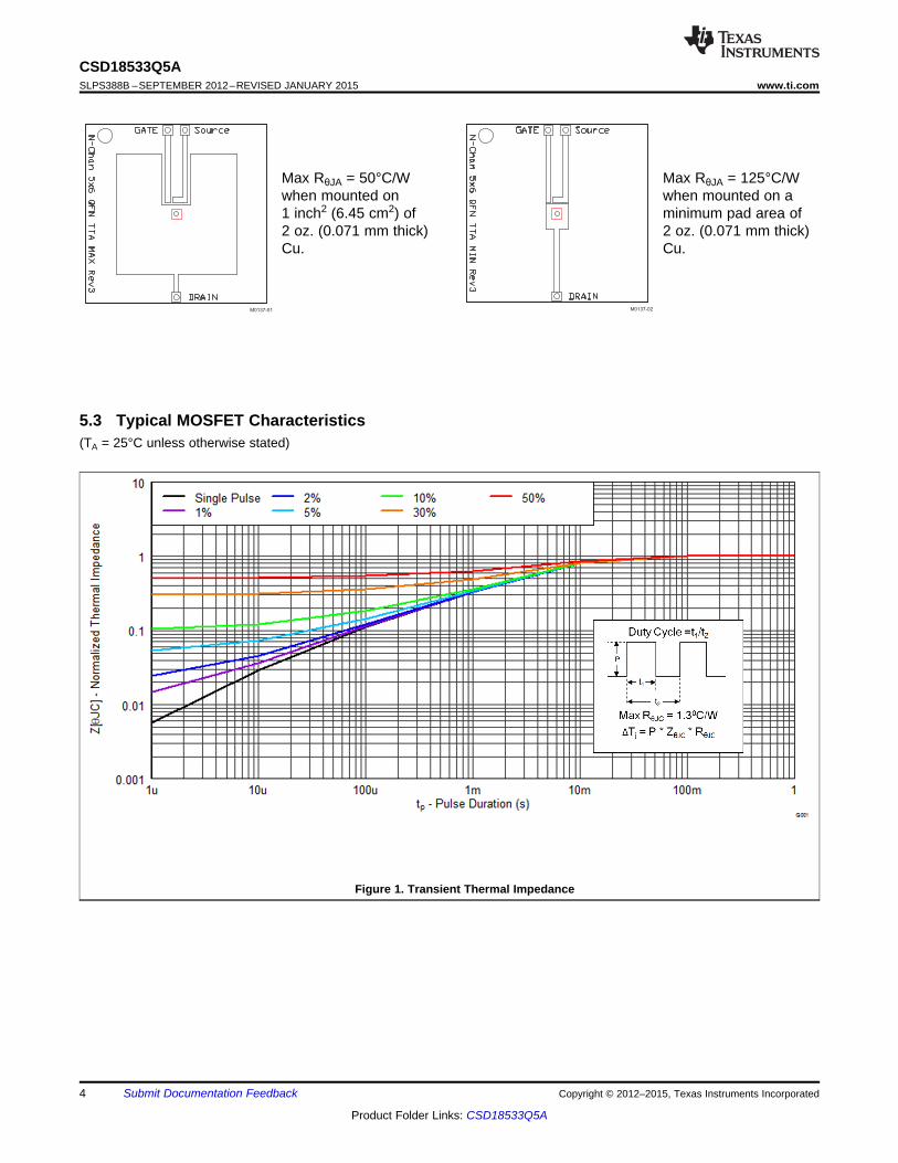
GATE Source
DRAIN
N-Chan 5x6 QFN TTA MAX Rev3
M0137-01
GATE Source
DRAIN
N-Chan 5x6 QFN TTA MIN Rev3
M0137-02
CSD18533Q5ASLPS388B –SEPTEMBER 2012–REVISED JANUARY 2015 www.ti.com
Max RθJA = 50°C/W Max RθJA = 125°C/Wwhen mounted on when mounted on a1 inch2 (6.45 cm2) of minimum pad area of2 oz. (0.071 mm thick) 2 oz. (0.071 mm thick)Cu. Cu.
5.3 Typical MOSFET Characteristics(TA = 25°C unless otherwise stated)
Figure 1. Transient Thermal Impedance
4 Submit Documentation Feedback Copyright © 2012–2015, Texas Instruments Incorporated
Product Folder Links: CSD18533Q5A
0.6
0.8
1
1.2
1.4
1.6
1.8
2
2.2
2.4
2.6
−75 −25 25 75 125 175TC - Case Temperature (ºC)
VG
S(th
) - T
hres
hold
Vol
tage
(V
)
ID = 250uA
G001
0
2
4
6
8
10
12
14
16
0 2 4 6 8 10 12 14 16 18 20VGS - Gate-to- Source Voltage (V)
RD
S(o
n) -
On-
Sta
te R
esis
tanc
e (
mΩ
) TC = 25°C Id = 18ATC = 125ºC Id = 18A
G001
0
2
4
6
8
10
0 5 10 15 20 25 30Qg - Gate Charge (nC)
VG
S -
Gat
e-to
-Sou
rce
Vol
tage
(V
) ID = 18AVDS = 30V
G001
10
100
1000
10000
50000
0 10 20 30VDS - Drain-to-Source Voltage (V)
C −
Cap
acita
nce
(pF
)Ciss = Cgd + CgsCoss = Cds + CgdCrss = Cgd
G001
0
20
40
60
80
100
120
140
160
180
200
0 0.5 1 1.5 2VDS - Drain-to-Source Voltage (V)
I DS -
Dra
in-t
o-S
ourc
e C
urre
nt (
A)
VGS =10VVGS =6.5VVGS =4.5V
G001
0
20
40
60
80
100
120
140
160
180
200
0 1 2 3 4 5VGS - Gate-to-Source Voltage (V)
I DS -
Dra
in-t
o-S
ourc
e C
urre
nt (
A)
TC = 125°CTC = 25°CTC = −55°C
VDS = 5V
G001
CSD18533Q5Awww.ti.com SLPS388B –SEPTEMBER 2012–REVISED JANUARY 2015
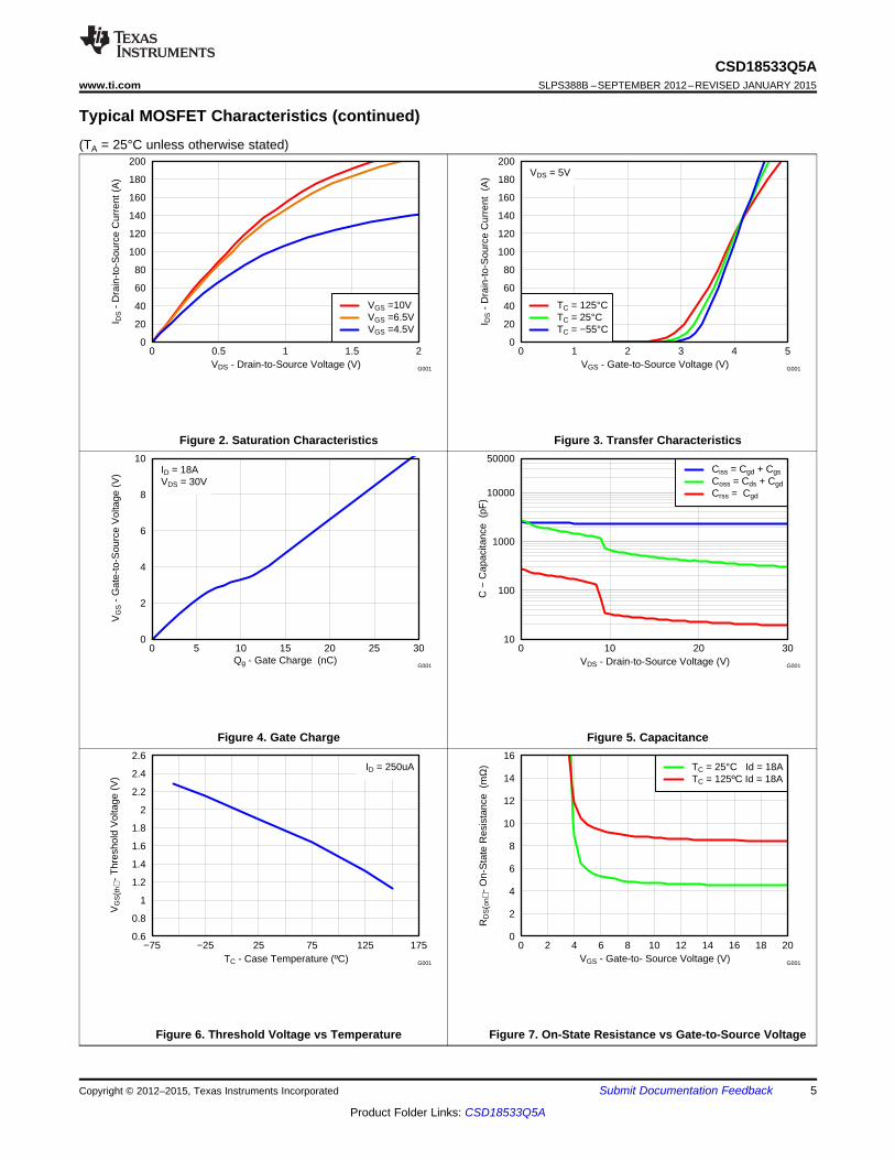
Typical MOSFET Characteristics (continued)(TA = 25°C unless otherwise stated)
Figure 2. Saturation Characteristics Figure 3. Transfer Characteristics
Figure 4. Gate Charge Figure 5. Capacitance
Figure 6. Threshold Voltage vs Temperature Figure 7. On-State Resistance vs Gate-to-Source Voltage
Copyright © 2012–2015, Texas Instruments Incorporated Submit Documentation Feedback 5
Product Folder Links: CSD18533Q5A
0
20
40
60
80
100
120
140
−50 −25 0 25 50 75 100 125 150 175TC - Case Temperature (ºC)
I DS -
Dra
in-
to-
Sou
rce
Cur
rent
(A
)
G001
0.1
1
10
100
1000
5000
0.1 1 10 100VDS - Drain-to-Source Voltage (V)
I DS -
Dra
in-t
o-S
ourc
e C
urre
nt (
A) 10us
100us1ms10ms
DC
Single PulseMax RthetaJC = 1.3ºC/W
G001
10
100
0.01 0.1 1TAV - Time in Avalanche (mS)
I AV -
Pea
k A
vala
nche
Cur
rent
(A
)
TC = 25ºCTC = 125ºC
G001
0.3
0.6
0.9
1.2
1.5
1.8
2.1
2.4
−75 −25 25 75 125 175TC - Case Temperature (ºC)
Nor
mal
ized
On-
Sta
te R
esis
tanc
e
VGS = 4.5VVGS = 10V
ID =18A
G001
0.0001
0.001
0.01
0.1
1
10
100
0 0.2 0.4 0.6 0.8 1VSD − Source-to-Drain Voltage (V)
I SD −
Sou
rce-
to-D
rain
Cur
rent
(A
) TC = 25°CTC = 125°C
G001
CSD18533Q5ASLPS388B –SEPTEMBER 2012–REVISED JANUARY 2015 www.ti.com
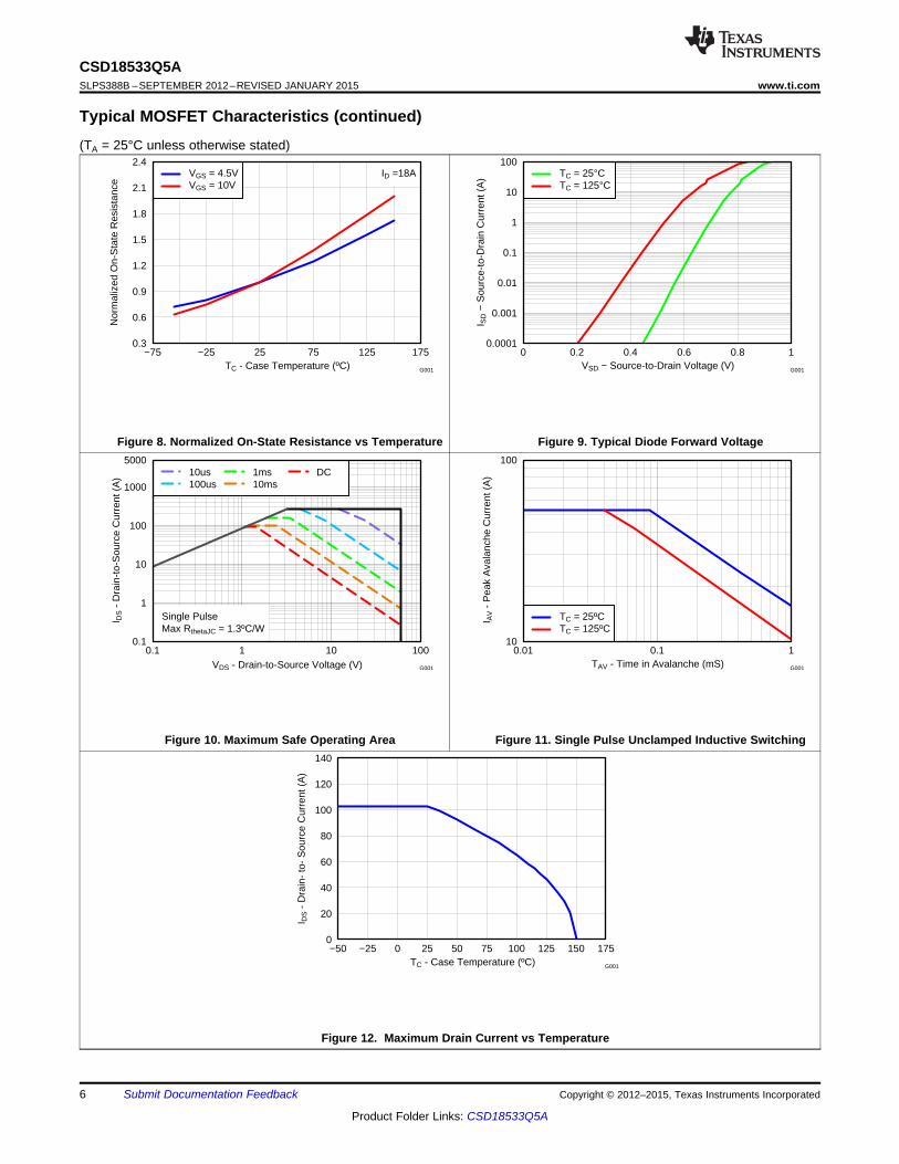
Typical MOSFET Characteristics (continued)(TA = 25°C unless otherwise stated)
Figure 8. Normalized On-State Resistance vs Temperature Figure 9. Typical Diode Forward Voltage
Figure 10. Maximum Safe Operating Area Figure 11. Single Pulse Unclamped Inductive Switching
Figure 12. Maximum Drain Current vs Temperature
6 Submit Documentation Feedback Copyright © 2012–2015, Texas Instruments Incorporated
Product Folder Links: CSD18533Q5A
CSD18533Q5Awww.ti.com SLPS388B –SEPTEMBER 2012–REVISED JANUARY 2015
6 Device and Documentation Support
6.1 TrademarksNexFET is a trademark of Texas Instruments.All other trademarks are the property of their respective owners.
6.2 Electrostatic Discharge CautionThese devices have limited built-in ESD protection. The leads should be shorted together or the device placed in conductive foamduring storage or handling to prevent electrostatic damage to the MOS gates.
6.3 GlossarySLYZ022 — TI Glossary.
This glossary lists and explains terms, acronyms, and definitions.
Copyright © 2012–2015, Texas Instruments Incorporated Submit Documentation Feedback 7
Product Folder Links: CSD18533Q5A
12
556
781
42
3
34
67
8
CSD18533Q5ASLPS388B –SEPTEMBER 2012–REVISED JANUARY 2015 www.ti.com
7 Mechanical, Packaging, and Orderable InformationThe following pages include mechanical, packaging, and orderable information. This information is the mostcurrent data available for the designated devices. This data is subject to change without notice and revision ofthis document. For browser-based versions of this data sheet, refer to the left-hand navigation.
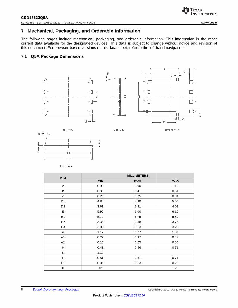
7.1 Q5A Package Dimensions
MILLIMETERSDIM
MIN NOM MAXA 0.90 1.00 1.10b 0.33 0.41 0.51c 0.20 0.25 0.34
D1 4.80 4.90 5.00D2 3.61 3.81 4.02E 5.90 6.00 6.10E1 5.70 5.75 5.80E2 3.38 3.58 3.78E3 3.03 3.13 3.23e 1.17 1.27 1.37e1 0.27 0.37 0.47e2 0.15 0.25 0.35H 0.41 0.56 0.71K 1.10L 0.51 0.61 0.71L1 0.06 0.13 0.20θ 0° 12°
8 Submit Documentation Feedback Copyright © 2012–2015, Texas Instruments Incorporated
Product Folder Links: CSD18533Q5A
4.310
58 1
4
3.020
0.500
1.5701.270
0.615 1.105
0.500
1.585 1.235
0.620
0.500
(0.020) 8x
(0.020)
(0.020) 8x
(0.024)
(0.062)
4x (0.050)
(0.044)(0.024)
(0.119)
(0.062) (0.049)
(0.170)
0.385(0.015)
F10
F11
F6 F7
F5
F9
F4
F8
145
8
M0139-01
F2
F3
F1
CSD18533Q5Awww.ti.com SLPS388B –SEPTEMBER 2012–REVISED JANUARY 2015
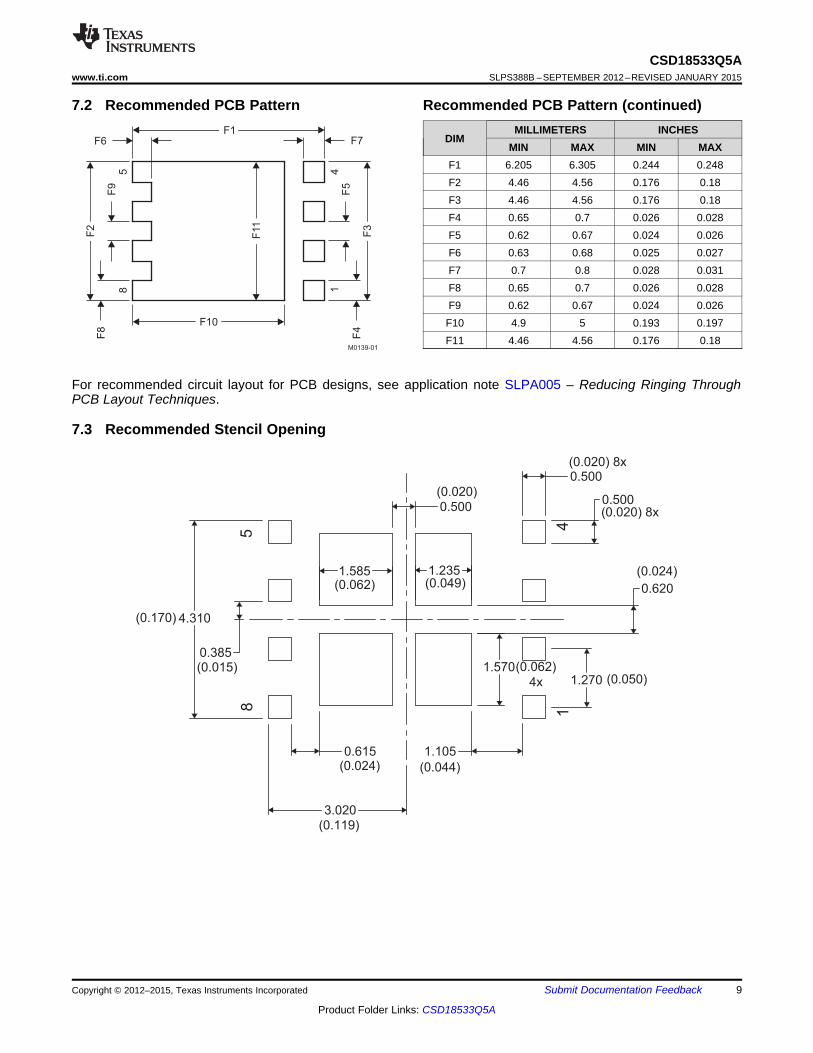
7.2 Recommended PCB Pattern Recommended PCB Pattern (continued)MILLIMETERS INCHES
DIMMIN MAX MIN MAX
F1 6.205 6.305 0.244 0.248F2 4.46 4.56 0.176 0.18F3 4.46 4.56 0.176 0.18F4 0.65 0.7 0.026 0.028F5 0.62 0.67 0.024 0.026F6 0.63 0.68 0.025 0.027F7 0.7 0.8 0.028 0.031F8 0.65 0.7 0.026 0.028F9 0.62 0.67 0.024 0.026F10 4.9 5 0.193 0.197F11 4.46 4.56 0.176 0.18
For recommended circuit layout for PCB designs, see application note SLPA005 – Reducing Ringing ThroughPCB Layout Techniques.
7.3 Recommended Stencil Opening
Copyright © 2012–2015, Texas Instruments Incorporated Submit Documentation Feedback 9
Product Folder Links: CSD18533Q5A
Ø 1.50+0.10–0.00
4.00 ±0.10 (See Note 1)
1.7
5 ±
0.1
0
R 0.30 TYP
Ø 1.50 MIN
A0
K0
0.30 ±0.05
R 0.30 MAX
A0 = 6.50 ±0.10B0 = 5.30 ±0.10K0 = 1.40 ±0.10
M0138-01
2.00 ±0.05
8.00 ±0.10
B0
12.0
0 ±
0.3
0
5.5
0 ±
0.0
5
CSD18533Q5ASLPS388B –SEPTEMBER 2012–REVISED JANUARY 2015 www.ti.com
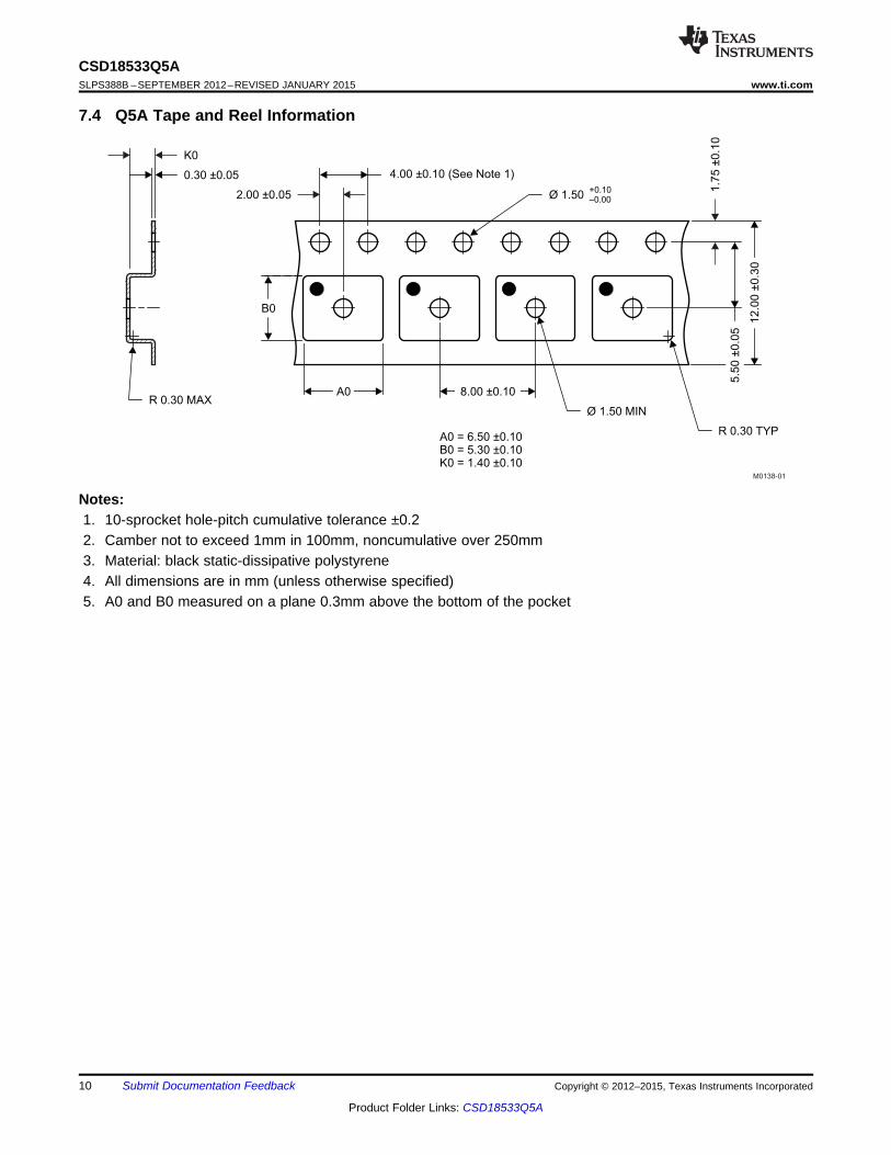
7.4 Q5A Tape and Reel Information
Notes:1. 10-sprocket hole-pitch cumulative tolerance ±0.22. Camber not to exceed 1mm in 100mm, noncumulative over 250mm3. Material: black static-dissipative polystyrene4. All dimensions are in mm (unless otherwise specified)5. A0 and B0 measured on a plane 0.3mm above the bottom of the pocket
spacer
10 Submit Documentation Feedback Copyright © 2012–2015, Texas Instruments Incorporated
Product Folder Links: CSD18533Q5A
PACKAGE OPTION ADDENDUM
www.ti.com 1-Apr-2015
Addendum-Page 1
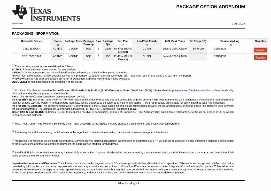
PACKAGING INFORMATION
Orderable Device Status(1)
Package Type PackageDrawing
Pins PackageQty
Eco Plan(2)
Lead/Ball Finish(6)
MSL Peak Temp(3)
Op Temp (°C) Device Marking(4/5)
Samples
CSD18533Q5A ACTIVE VSONP DQJ 8 2500 Pb-Free (RoHSExempt)
CU SN Level-1-260C-UNLIM -55 to 150 CSD18533
CSD18533Q5AT ACTIVE VSONP DQJ 8 250 Pb-Free (RoHSExempt)
CU SN Level-1-260C-UNLIM CSD18533
(1) The marketing status values are defined as follows:ACTIVE: Product device recommended for new designs.LIFEBUY: TI has announced that the device will be discontinued, and a lifetime-buy period is in effect.NRND: Not recommended for new designs. Device is in production to support existing customers, but TI does not recommend using this part in a new design.PREVIEW: Device has been announced but is not in production. Samples may or may not be available.OBSOLETE: TI has discontinued the production of the device.
(2) Eco Plan - The planned eco-friendly classification: Pb-Free (RoHS), Pb-Free (RoHS Exempt), or Green (RoHS & no Sb/Br) - please check http://www.ti.com/productcontent for the latest availabilityinformation and additional product content details.TBD: The Pb-Free/Green conversion plan has not been defined.Pb-Free (RoHS): TI's terms "Lead-Free" or "Pb-Free" mean semiconductor products that are compatible with the current RoHS requirements for all 6 substances, including the requirement thatlead not exceed 0.1% by weight in homogeneous materials. Where designed to be soldered at high temperatures, TI Pb-Free products are suitable for use in specified lead-free processes.Pb-Free (RoHS Exempt): This component has a RoHS exemption for either 1) lead-based flip-chip solder bumps used between the die and package, or 2) lead-based die adhesive used betweenthe die and leadframe. The component is otherwise considered Pb-Free (RoHS compatible) as defined above.Green (RoHS & no Sb/Br): TI defines "Green" to mean Pb-Free (RoHS compatible), and free of Bromine (Br) and Antimony (Sb) based flame retardants (Br or Sb do not exceed 0.1% by weightin homogeneous material)
(3) MSL, Peak Temp. - The Moisture Sensitivity Level rating according to the JEDEC industry standard classifications, and peak solder temperature.
(4) There may be additional marking, which relates to the logo, the lot trace code information, or the environmental category on the device.
(5) Multiple Device Markings will be inside parentheses. Only one Device Marking contained in parentheses and separated by a "~" will appear on a device. If a line is indented then it is a continuationof the previous line and the two combined represent the entire Device Marking for that device.
(6) Lead/Ball Finish - Orderable Devices may have multiple material finish options. Finish options are separated by a vertical ruled line. Lead/Ball Finish values may wrap to two lines if the finishvalue exceeds the maximum column width.
Important Information and Disclaimer:The information provided on this page represents TI's knowledge and belief as of the date that it is provided. TI bases its knowledge and belief on informationprovided by third parties, and makes no representation or warranty as to the accuracy of such information. Efforts are underway to better integrate information from third parties. TI has taken andcontinues to take reasonable steps to provide representative and accurate information but may not have conducted destructive testing or chemical analysis on incoming materials and chemicals.TI and TI suppliers consider certain information to be proprietary, and thus CAS numbers and other limited information may not be available for release.
PACKAGE OPTION ADDENDUM
www.ti.com 1-Apr-2015
Addendum-Page 2
In no event shall TI's liability arising out of such information exceed the total purchase price of the TI part(s) at issue in this document sold by TI to Customer on an annual basis.
IMPORTANT NOTICE
Texas Instruments Incorporated and its subsidiaries (TI) reserve the right to make corrections, enhancements, improvements and otherchanges to its semiconductor products and services per JESD46, latest issue, and to discontinue any product or service per JESD48, latestissue. Buyers should obtain the latest relevant information before placing orders and should verify that such information is current andcomplete. All semiconductor products (also referred to herein as “components”) are sold subject to TI’s terms and conditions of salesupplied at the time of order acknowledgment.TI warrants performance of its components to the specifications applicable at the time of sale, in accordance with the warranty in TI’s termsand conditions of sale of semiconductor products. Testing and other quality control techniques are used to the extent TI deems necessaryto support this warranty. Except where mandated by applicable law, testing of all parameters of each component is not necessarilyperformed.TI assumes no liability for applications assistance or the design of Buyers’ products. Buyers are responsible for their products andapplications using TI components. To minimize the risks associated with Buyers’ products and applications, Buyers should provideadequate design and operating safeguards.TI does not warrant or represent that any license, either express or implied, is granted under any patent right, copyright, mask work right, orother intellectual property right relating to any combination, machine, or process in which TI components or services are used. Informationpublished by TI regarding third-party products or services does not constitute a license to use such products or services or a warranty orendorsement thereof. Use of such information may require a license from a third party under the patents or other intellectual property of thethird party, or a license from TI under the patents or other intellectual property of TI.Reproduction of significant portions of TI information in TI data books or data sheets is permissible only if reproduction is without alterationand is accompanied by all associated warranties, conditions, limitations, and notices. TI is not responsible or liable for such altereddocumentation. Information of third parties may be subject to additional restrictions.Resale of TI components or services with statements different from or beyond the parameters stated by TI for that component or servicevoids all express and any implied warranties for the associated TI component or service and is an unfair and deceptive business practice.TI is not responsible or liable for any such statements.Buyer acknowledges and agrees that it is solely responsible for compliance with all legal, regulatory and safety-related requirementsconcerning its products, and any use of TI components in its applications, notwithstanding any applications-related information or supportthat may be provided by TI. Buyer represents and agrees that it has all the necessary expertise to create and implement safeguards whichanticipate dangerous consequences of failures, monitor failures and their consequences, lessen the likelihood of failures that might causeharm and take appropriate remedial actions. Buyer will fully indemnify TI and its representatives against any damages arising out of the useof any TI components in safety-critical applications.In some cases, TI components may be promoted specifically to facilitate safety-related applications. With such components, TI’s goal is tohelp enable customers to design and create their own end-product solutions that meet applicable functional safety standards andrequirements. Nonetheless, such components are subject to these terms.No TI components are authorized for use in FDA Class III (or similar life-critical medical equipment) unless authorized officers of the partieshave executed a special agreement specifically governing such use.Only those TI components which TI has specifically designated as military grade or “enhanced plastic” are designed and intended for use inmilitary/aerospace applications or environments. Buyer acknowledges and agrees that any military or aerospace use of TI componentswhich have not been so designated is solely at the Buyer's risk, and that Buyer is solely responsible for compliance with all legal andregulatory requirements in connection with such use.TI has specifically designated certain components as meeting ISO/TS16949 requirements, mainly for automotive use. In any case of use ofnon-designated products, TI will not be responsible for any failure to meet ISO/TS16949.
Products ApplicationsAudio www.ti.com/audio Automotive and Transportation www.ti.com/automotiveAmplifiers amplifier.ti.com Communications and Telecom www.ti.com/communicationsData Converters dataconverter.ti.com Computers and Peripherals www.ti.com/computersDLP® Products www.dlp.com Consumer Electronics www.ti.com/consumer-appsDSP dsp.ti.com Energy and Lighting www.ti.com/energyClocks and Timers www.ti.com/clocks Industrial www.ti.com/industrialInterface interface.ti.com Medical www.ti.com/medicalLogic logic.ti.com Security www.ti.com/securityPower Mgmt power.ti.com Space, Avionics and Defense www.ti.com/space-avionics-defenseMicrocontrollers microcontroller.ti.com Video and Imaging www.ti.com/videoRFID www.ti-rfid.comOMAP Applications Processors www.ti.com/omap TI E2E Community e2e.ti.comWireless Connectivity www.ti.com/wirelessconnectivity
Mailing Address: Texas Instruments, Post Office Box 655303, Dallas, Texas 75265Copyright © 2016, Texas Instruments Incorporated