Conductivity Lab Overview
41
Conductivity Lab Overview Ben Nachumi February 11, 2013 1 Welcome to the solid state electrical conductivity lab! The electrical conductance (symbol: S ) of a wire tells how much current I the wire carries when a voltage V is applied across its ends: S = I/V . The conductance of a given wire is related to the material property of conductivity (σ). A particular wire, with length l, area A, made of a material of conductivity σ, will have a conductance S = σ × A/l. σ is measured in units of current per unit cross-sectional area per unit of applied field. Of course the conductance is the material property that makes metals metallic and insulators insulate, depending on the values that it takes. It would be hard to overstate its techno- logical significance. In practice, one often hears about the electrical resistance, R. The resistance of a piece of material is the ratio of electrical voltage to current: R = V/I . Obviously, R =1/S . The related material property is the resistivity (ρ), which is the inverse of the conductivity (ρ =1/σ). For a wire of length l and cross-sectional area A, ρ is defined by the relation R = ρ × l/A. The separation of bulk properties from geometric specifics is a good approximation for macroscopic samples, and allows people to make differently rated resistors from the same kind of wire. This simplifying separability breaks down when wires are made atomically thin, but you can see many important effects which are best explained in terms of quantum mechanics even with comparatively big chunks of material. 1 Within a single piece of stuff, the electrical conductivity/resistivity is generally a func- tion of both the applied electromagnetic fields and the temperature. It is also a function of whether the atoms are in a uniform crystal lattice, or disordered. The physical models that will frame your data analysis apply best to crystalline systems, and cover the depen- dence on the magnitude (but not the direction) of the applied electrical field at a given 1 You can measure some more exotic effects in the conductivity of atomically thin wires and nearly atomically thin sheets in the Quantum Conductance and Quantum Hall Effect experiments, respectively. 1
Transcript of Conductivity Lab Overview
Conductivity Lab Overview
Ben Nachumi
February 11, 2013
1 Welcome to the solid state electrical conductivity lab!
The electrical conductance (symbol: S) of a wire tells how much current I the wire carrieswhen a voltage V is applied across its ends: S = I/V . The conductance of a given wireis related to the material property of conductivity (σ). A particular wire, with length l,area A, made of a material of conductivity σ, will have a conductance S = σ × A/l. σis measured in units of current per unit cross-sectional area per unit of applied field. Ofcourse the conductance is the material property that makes metals metallic and insulatorsinsulate, depending on the values that it takes. It would be hard to overstate its techno-logical significance.
In practice, one often hears about the electrical resistance, R. The resistance of a pieceof material is the ratio of electrical voltage to current: R = V/I. Obviously, R = 1/S.The related material property is the resistivity (ρ), which is the inverse of the conductivity(ρ = 1/σ). For a wire of length l and cross-sectional area A, ρ is defined by the relationR = ρ× l/A.
The separation of bulk properties from geometric specifics is a good approximation formacroscopic samples, and allows people to make differently rated resistors from the samekind of wire. This simplifying separability breaks down when wires are made atomicallythin, but you can see many important effects which are best explained in terms of quantummechanics even with comparatively big chunks of material.1
Within a single piece of stuff, the electrical conductivity/resistivity is generally a func-tion of both the applied electromagnetic fields and the temperature. It is also a functionof whether the atoms are in a uniform crystal lattice, or disordered. The physical modelsthat will frame your data analysis apply best to crystalline systems, and cover the depen-dence on the magnitude (but not the direction) of the applied electrical field at a given
1You can measure some more exotic effects in the conductivity of atomically thin wires and nearlyatomically thin sheets in the Quantum Conductance and Quantum Hall Effect experiments, respectively.
1

temperature, and how this changes when the temperature of the sample is uniformly raisedand lowered. For the samples you will be studying in this lab, you can ignore the effectsof shape and even of thermal expansion,2 and can therefore treat a measurement of R asa measurement of ρ and a measurement of S as a measurement of σ.
There are several kinds of material to look at. The first and simplest effect to see(though not the easiest to understand) is the transition temperature of a piece of super-conducting wire. For the second, you will find and fit for the Debye temperature of plat-inum. Together, these should take up two to three meetings. Further possible experimentsinclude: actually making and testing a sample of a particular high-TC superconductor;measuring the band gap in a semiconductor from the conductivity of a diode; and lookingfor resistive evidence of the ferromagnetic transition in a piece of nickel.3
2 Overview of the Techniques
This is the rig block diagram for the low-temperature measurement. It’s pretty straight-forward: the sample sits in a refrigerator, with leads to measure its temperature andelectrical resistance. The vacuum insulates the very cold inside of the refrigerator from itsroom-temperature outside. But there are some subtleties, which we shall now describe.
2.1 The 4-Wire Technique and Alternation
A voltmeter doesn’t know what it’s connected to. If you were to measure the voltage acrossthe sample using the same leads with which you applied the probing current, you wouldalso measure the voltage drop through the current leads. Since the leads can be long andthe sample resistance may be small, this can be a very significant source of measurementerror. The simplest solution to this problem is to apply the current with one pair of wires,and measure the voltage with a second pair.
Another source of extraneous voltage is the Seebeck effect due to the thermal gradientdown the voltage leads. Warm electrons diffuse faster down the wire, leading to a voltageproportional to the temperature difference. This material-dependent effect is the basisfor the thermocouple thermometer, but for conductors (with small voltage signals) it’s anuisance because inevitable asymmetries in the lead wires will lead to a voltage offset. The
2This is because the thermal expansion of a solid is due to phonon anharmonicity, or phonon-phononinteractions. In the absence of a structural phase transition, and well below a material’s melting point,these are a smaller correction upon (of second-order to) the linear effects of phonon density you shall bestudying in metals. You might be able to see the effect of the thermal expansion on the energy gap in thesemiconductor measurement, though again, this effect is on the order of 10%.
3You might also be interested in developing a new measurement for this lab. If there is a particularmaterial or technique you would like to try, let us know!
2

Figure 1: Rig Block Diagram.
Sample
Current Current
Voltage Voltage
To meters To meters
Figure 2: Four-Wire Schematic.
3

Figure 3: The control boxes for the 4-wire measurement: Top: Keithley 6220 precisioncurrent source; Bottom: Keithley 2812A nanovoltmeter; Left: Lakeshore temperature con-troller.
Rearbox.jpg
Figure 4: The rear of the 6220/2812 pair, set up for Delta measurements. For diodemeasurements, the two serial connections between them are replaced by a GPIB cable.4
solution to this problem is to alternate the direction of the applied current. In the averageof the two measured voltages, this and other asymmetries cancel out.
The Keithley current source and voltmeter can be set up to alternate in what Keithleycalls“Delta mode” (more information is in the Keithley manual). You can initiate thesemeasurements either from the Keithley front panels, or from the scripts we have set upfor you in Matlab (see below). However for measurements of diodes and other intrinsicallyasymmetric devices, you would use the Keithley in DC mode.
At the start of the experiment, the Keithley should already be set up in Delta mode.For directions on how to switch over to DC mode, see section 3.6 below.
2.2 Refrigeration
To get samples down to low temperatures, you have the use of a closed-cycle helium refrig-erator. Compared to the cryostats used in the other low temperature labs, this system ismore like a refrigerator in the sense of a kitchen refrigerator, with a compression/expansioncycle of a refrigerant fluid. The important details of how to operate this rather complicatedbit of machinery are discussed in the CTI Refrigerator Manual. However, if everythingis working properly, the instructions in section 3.5 (Cooling Down) should suffice.
For now, note that the refrigerator comes in two parts, connected by pressurized heliumgas hoses. The big box contains a large pre-compressor; the heavy object to which theseleads go is called the cold head. It is so clunky because it contains a motor that drivesheat-exchanging pistons back and forth. The coldest part of the cold head is at the tip ofthe cold finger. This is where the sample assembly goes. Note that all of the lead wiresare thermally anchored all the way down the cold finger to prevent unmitigated thermalconduction from the feedthrough plugs to the sample.
Next, two heat shields are placed around the sample. These fairly isothermal surfacesboth slow radiative heating from the tip of the cold finger and maintain the environmentaround the sample at a constant temperature. Finally comes the outer tail, which pressure-seals to the feedthrough housing around the shielded cold finger. Once this is done, a vanepump gets most of the atmosphere out of the sealed-off space (otherwise the remnant vaporpressure of the eventually frozen air would leak heat to the sample). At this point, witheverything canned up and evacuated, you are ready to start the refrigerator.
Unburdened with a heat load, the refrigerator is meant to cool the tip of the cold fingerdown to around 10K over 60− 90 minutes.
5

Figure 5: The cold head. The sample mounts to the copper backing at the top, and theleads are soldered to the pins.
3 Required Measurements
3.1 Calibrating Thermometers
How do you measure temperatures on an absolute scale? An ideal gas bulb and a blackbodyspectrum are “model independent” standards, but these aren’t really convenient. One usu-ally uses secondary devices whose calibrations are ultimately traceable to a standard. Onecommon device is a resistor like a twist of platinum wire. At high temperatures, the resis-tance versus temperature of many metals is quite linear. But below 30 K, the resistivity ofa platinum sample becomes noticeably less linear and drops away as phonons freeze out.On the other hand, the resistivity of a semiconductor diode increases as thermally excitedcarriers freeze out. Hence, just where platinum thermometers become useless, the appro-priate semiconductor thermometer becomes more sensitive. In principle, one calibratesthe temperature/voltage function of the diode using a gas bulb thermometer, or against apreviously calibrated Pt resistor, and generates an interpolation table.
Your refrigerator currently has two diode thermometers installed. These are fairly stan-dardized and almost perfectly interchangeable. The production is well-enough controlledthat the interpolation curve can be fixed to within a tolerance of about a Kelvin with justtwo fixed measurements.
6
The calibration of these thermometers tends to drift over a period of months. If youare the first group doing this experiment in a while, you should recalibrate them usingthe SOFT CAL procedure detailed in the Lakeshore manual. Read it. For temperaturestandards, you will can dunk the diodes together into ice water (273.15K) and liquidnitrogen (77.3K). After the calibration is complete, let the thermometers heat up, andmake sure that they agree with the mercury thermometer on the room temperature.
3.2 Sample Mounting
For the usual samples (Pt wire, SC wire, diode) the samples should already be solderedto four leads with pins for the plugs on the copper backing. Existing samples are gluedbetween spacers of flat thermally conductive electrical insulators: sapphire disks, or, if thoserun out, pieces of mica. Each spacer is varnished into contact with a diode thermometer.One of the thermometers sits atop a resistive heater (just some wire wound on a piece ofmica) which in turn sits on the coldest part of the refrigerator.
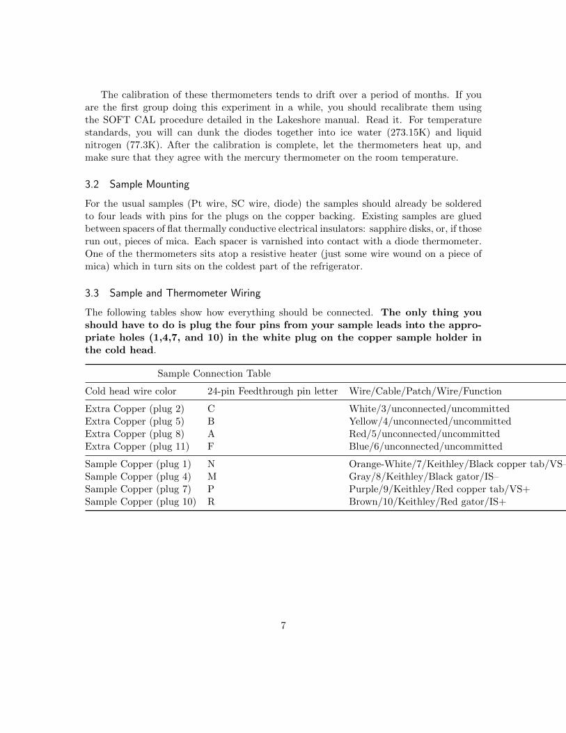
3.3 Sample and Thermometer Wiring
The following tables show how everything should be connected. The only thing youshould have to do is plug the four pins from your sample leads into the appro-priate holes (1,4,7, and 10) in the white plug on the copper sample holder inthe cold head.
Sample Connection Table
Cold head wire color 24-pin Feedthrough pin letter Wire/Cable/Patch/Wire/Function
Extra Copper (plug 2) C White/3/unconnected/uncommittedExtra Copper (plug 5) B Yellow/4/unconnected/uncommittedExtra Copper (plug 8) A Red/5/unconnected/uncommittedExtra Copper (plug 11) F Blue/6/unconnected/uncommitted
Sample Copper (plug 1) N Orange-White/7/Keithley/Black copper tab/VS–Sample Copper (plug 4) M Gray/8/Keithley/Black gator/IS–Sample Copper (plug 7) P Purple/9/Keithley/Red copper tab/VS+Sample Copper (plug 10) R Brown/10/Keithley/Red gator/IS+
7

Figure 6: How the samples are mounted on the copper sample holder. The two thermome-ters bracket the sample temperature. The sapphire layers provide good thermal contactand electrical insulation.
Figure 7: Pin diagram for the terminals on the copper sample holder.
8

Thermometry Feedthrough Connection Table
Cold head wire color 10-pin Feedthrough pin letter Wire/Patch/Cable/Wire/Function
Heater Copper (backing 9) A Red/11/Lakeshore A/White/H1Heater Copper (backing 10) H Purple/12/Lakeshore A/Yellow/H2
Diode A Red (backing 1) J White/13/Lakeshore A/Black/IA–Diode A Green (backing 2) C Green/14/Lakeshore A/Blue/VA–Diode A Black (backing 3) G Orange/15/Lakeshore A/Green/VA+Diode A Gold (backing 4) B Black/16/Lakeshore A/Red/IA+
Diode B Red (backing 5) K Brown/17/Lakeshore B/Orange/IB–Diode B Green (backing 6) D Yellow/18/Lakeshore B/Red/VB–Diode B Black (backing 7) F Gray/19/Lakeshore B/Black/VB+Diode B Gold (backing 8) E Blue/20/Lakeshore B/Blue/IB+
3.4 Preliminary Tests
After plugging in the sample pins, you should go through the following checklist:
• TEST THE I/V CONNECTIONS! With the Keithley boxes both off, use the hand-held DVM to test the four sample connections. (Across the standard Pt sample,you should see the room temperature resistance of about 108Ω). Turn the KeithleyDVM/Current Source on and put them into in DELTA mode (hit DELTA). Whenthe current source says it’s ready, hit ENTER. You should be able to read a voltage,and from the voltage and the current applied, calculate a resistance. Is the resistanceyou read in fair agreement with what you got when you tested your sample leads?To get out of DELTA mode hit EXIT.
• TEST THE HEATER CONNECTIONS! With the Lakeshore off, put the DVM acrossthe heater patch points. You should see a resistance on the order of 10− 200Ω (theprecise value will depend on the precise heater).
• TEST THE THERMOMETER CONNECTIONS! Turn on the Lakeshore, and makesure your thermometers are reading and are in reasonable agreement with each other.They should respond when, say, you gently touch the sample stack with your fingertip.
3.5 Cooling Down
Now you are ready to refrigerate!
• Can up the sample. Screw down the copper isothermal cap (be very careful not topinch any wires in the process). After doing this, make sure all of the connectionsare still behaving sensibly. Then screw down the silvery heat shield.
9
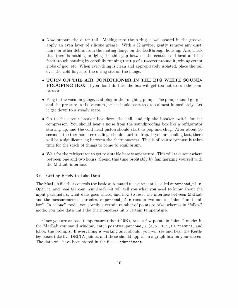
• Now prepare the outer tail. Making sure the o-ring is well seated in the groove,apply an even layer of silicone grease. With a Kimwipe, gently remove any dust,hairs, or other debris from the mating flange on the feedthrough housing. Also checkthat there is nothing bridging the thin gap between the central cold head and thefeedthrough housing by carefully running the tip of a tweezer around it, wiping errantglobs of goo, etc. When everything is clean and appropriately isolated, place the tailover the cold finger so the o-ring sits on the flange.
• TURN ON THE AIR CONDITIONER IN THE BIG WHITE SOUND-PROOFING BOX. If you don’t do this, the box will get too hot to run the com-pressor.
• Plug in the vacuum gauge, and plug in the roughing pump. The pump should gurgle,and the pressure in the vacuum jacket should start to drop almost immediately. Letit get down to a steady state.
• Go to the circuit breaker box down the hall, and flip the breaker switch for thecompressor. You should hear a noise from the soundproofing box like a refrigeratorstarting up, and the cold head piston should start to pop and chug. After about 30seconds, the thermometer readings should start to drop. If you are cooling fast, therewill be a significant lag between the thermometers. This is of course because it takestime for the stack of things to come to equilibrium.
• Wait for the refrigerator to get to a stable base temperature. This will take somewherebetween one and two hours. Spend this time profitably by familiarizing yourself withthe MatLab interface.
3.6 Getting Ready to Take Data
The MatLab file that controls the basic automated measurement is called supercond_ul.m.Open it, and read the comment header–it will tell you what you need to know about theinput parameters, what data goes where, and how to reset the interface between MatLaband the measurement electronics. supercond_ul.m runs in two modes: “alone” and “fol-low”. In “alone” mode, you specify a certain number of points to take, whereas in “follow”mode, you take data until the thermometers hit a certain temperature.
Once you are at base temperature (about 10K), take a few points in “alone” mode: inthe MatLab command window, enter point=supercond_ul(a,5,.1,1,10,"test"), andfollow the prompts. If everything is working as it should, you will see and hear the Keith-ley boxes take five DELTA points, and these should appear in a graph box on your screen.The data will have been stored in the file . . . \data\test.
10

To get a sense of your signal-to-noise, take a couple of DELTA measurements usingdifferent excitation currents at the same temperature. Because higher currents will giveyou more significant digits, you will see less scatter in your data as the current increases.On the other hand, you don’t want to use a current that is too large, for this will heat upyour sample. For the very small bit of superconducting wire, you can probably get awaywith .01A. For the Pt sample, which has a room temperature resistance of about 100Ω,.001A is a safe bet.
Now turn your attention to the Lakeshore box. For manual control, it needs to bein LOCAL mode. You can toggle between LOCAL and REMOTE by hitting the LO-CAL/REMOTE button on the front panel: the “R” in the upper right hand corner of theLCD display indicates when the box is in REMOTE mode, i.e. under compute control. Toslowly change temperatures when the cold head is near its base temperature, the LakeshorePID parameters ought to be small–less than or equal to 1.0. In LOCAL mode, you cancheck the PID settings by pressing the P,I, or D buttons on the front panel.
Now control the sample temperature. In LOCAL mode, press SET POINT, and entera set point not too far from base temperature–say, 15K. Then, and only then, use theHEATER RANGE button to turn the heater on LOW.
Use supercond_ul.m to take some more points while the temperature is changing. Inci-dentally, if you are unfamiliar with plotting data in MatLab, this is a good time to explorethose help menus and/or ask your TA for assistance.
3.7 Taking Data
If you are measuring the TC of the superconducting wire, your goal is to find the transitiontemperature as precisely as possible. This means controlling the temperature and movingin small increments. That’s about it! Your sample temperature will be bracketed by thetemperature on each thermometer, so the average of the two readings is probably the bestmeasure of the sample temperature.
When you measure the Pt sample, you need to scan from base temperature to roomtemperature. So after you have measured a few times around the base temperature, youshould invoke supercond_ul.m in “follow” mode with something likepoint=supercond_ul(f,290,.1,1,10,"filename"). Then shut off the compressor; thescript will keep taking and plotting measurements until one of the thermometers reaches290K.
Once you have taken your Pt data, you can fit for the Debye temperature using the
11
predefined fitting routine BGfit.m (see below).
3.8 File Management
To help keep a sensible record of the data taken and the students who took it, please setup a personal directory: . . . \student’s documents\[your_name]. When you take datawith MatLab, you will specify your data file names with that directory. You will also haveto add your directory to MatLab’s search path. The MatLab scripts that you will be usinglive in . . . \supercond\m.files. Before using them, copy them into your own directory.Then you can safely modify them if you must.
3.9 Provisions for Fitting Data
All of your data is read into MatLab, which also provides a powerful fitting environment.To fit your data, there are two files that you need. One is a master file that reads in yourdata, defines the starting parameters for your fit model, and calls a MatLab comparisonfunction, with the name of your second file as an input. The second file defines your fitmodel–it generates a theoretical function of the temperature. The MatLab comparisonfunction then takes the (R,T) data and compares it in a least-squares sense to your modelfunction, altering the parameters that you fed it to get the best match. Then it returnsthose parameters to the master file.
The pre-made example is the pair of files BGfit.m and BGcomp.m. This pair is whatyou will use to extract the Debye temperature in Pt from your R versus T graph. BGfit.mis the master file, which reads the data and invokes the comparison to the model definedin BGcomp.m, then plots the original data, along with the fitted function. BGfit.m withBGcomp.m should serve adequately as a model for you to follow in defining your own fits,which you will need to do if you measure the gap ∆ in a semiconductor.
4 Some Notes on the Elective Measurements
4.1 Non-Alternating Measurements (for Diodes)
For measurements of diodes, the alternating 4-wire measurement doesn’t make sense.Fortunately for diodes, the voltages you want to measure will be much larger than thevoltage difference due to the asymmetry of the lead wires, so you can get away with anon-alternating 4-wire measurement. Use the script diode_gpib.m. For it to work, youmust remove both the regular serial connection and the “fast serial” communication cablesbetween the 6220 and the 2182, reconnect them with a GPIB cable, and set the communi-cation modes of the 6220 and 2182 to GPIB.
12

GPIB.pdf
Figure 8: The Keithley boxes connected for Diode measurements.
13
Make sure you know which direction on the diode is “forward.” To avoiddamage to the diode and the concomitant bad data set, try not to apply toogreat a reverse current until and unless you want to see “reverse bias break-down”. Unless you are trying to break the diode, keep reverse currents to lessthan 1µA. For forward current, you probably don’t need to go much higher than a few mA.
The idea is to sit at a given temperature and trace out a representative current vs.voltage curve (of course, you will be setting the current and measuring the voltage). Thisrequires time for the temperature to settle, while your Lakeshore controller applies heatagainst the refrigerator’s cooling power. So plan on just a few measurements like (100K,150K, 200K, 250K, 300K). For these elevated temperatures, you will have to change thePID settings–try (10,10,10) as a starting configuration.
4.2 High Temperature Measurements and Furnace Use (for the TC of Ni)
For high temperature measurements, the sample sits on the end of a high-temperature in-sert made of alumina, a few millimeters away from a thermometer–in this case is a platinumresistor identical to the one you use as a sample in the Debye temperature measurement.You can safely extrapolate your resistance versus temperature measurement to high tem-peratures to estimate the temperature of the sample in the oven.
To make the measurements, you will have to patch the thermometer and sample inputsof the Lakeshore and the Keithley using terminals 1& 2 (for the Pt thermometer) and 21-24(for the sample measurement)–see the table below. Because there is only one thermometerfor this measurement, you will be using a different version of the automation script, callednickel.m. This reads the resistance of the nickel sample and the resistance of the platinumresistor.
Oven Insert Connection Table
Feeedout Wire Patch/Cable/Wire(s) Function
Green (black tape) 1/Lakeshore A/ Black IA–1/Lakeshore A/Blue VA–
Green 2/Lakeshore A/Green IA+2/Lakeshore A/Red VA+
Red (white tape) 21/Keithley/Black copper tab VS–Red (black tape) 22/Keithley/Black gator IS–Red (green tape) 23/Keithley/Red copper tab VS+Red 24/Keithley/Red gator IS+
14

The “Blue-M” box furnace is programmable–the necessary details are laid out in the markedpages of the Box Furnace Manual. The idea is to start from your high set temperatureand to ramp down to a few degrees above ambient (say, 30C) very slowly–the ramp rateshould not exceed 0.5C/minute. Make the set the temperature comfortably above TC , say450C, and wait for the Pt thermometer to equilibrate. Note that the temperature of the Ptthermometer will not necessarily be the same as the oven’s self-read temperature. Let theoven ramp to whatever temperature it thinks it is going to, but trust the Pt thermometer!
5 Making BSCCO
There are facilities for making fresh samples of the high temperature cuprate superconduc-tor, Bi2+xSr3−yCayCu2O8+δ (“BSCCO”) which (under the growth conditions you willuse) has a TC of around 90K.
You can bake up BSCCO as a powder, using the precursor materials BiO2 (bright yel-low), Sr2O3 and Ca2O3 (both white), and CuO (black). There is a scale, a mortar andpestle, crucibles, an oven, and a press for forming the BSCCO powder into pellets. At theappropriate time in the firing process, you will need liquid nitrogen for quenching.
The BSCCO process will take at least two weeks to complete. For most of this time,the mixed powders are in the kiln, slowly reacting. However you’ll need to schedule whenyou do the intermediate grinding and pressing. The grinding and pressing will occur inPupin 1313, where the fume hood and pellet press are located.
5.1 The Process
As you might imagine, the combination of these precursors leads to a very complicatedphase diagram. All sorts of intervening materials that can form at elevated temperatures.The phase diagram simplifies if all of the materials are forced to remain solid throughoutthe reaction. For this solid state reaction process to work, appropriate quantities of theprecursor powders are mixed intimately together so that the appropriate ions can diffusetogether.
So your first task is to figure out how much of each powder to mix. This of course de-pends on the precise composition of your material. Read through the provided referencesand look for the composition that yields the optimal TSC . Then figure out the mass of eachprecursor you’ll need to make about 10 g of sample. Carefully weigh out the precursors.Use weighing paper and weigh out each species individually. Wear gloves wheneverhandling chemicals.
15
Once you’ve weighed out your precursor powders, mix them thoroughly in the mor-tar. The mixing powders quickly look greenish grey. When thoroughly mixed, the powdershould look homogeneous under magnification, without any white particles of uncrushedcarbonate. Be prepared to mix for a while.
Once the powder is thoroughly mixed, fill it into an alumina crucible for calcination. Inthis step, the carbonates decompose and the precursors form tiny particles of the layeredcuprate. You can find the firing schedule in the Tsukamoto article, but you should alsolook at the Majewski article to see where you are in the phase diagram. To make phase-pure BSCCO by this method, it’s important that you never let the powder melt. To learnhow to control the furnace, consult the marked pages in the Box Furnace Manual. Theresulting powder should look black.
The next step is the annealing step. You’ll use the press to press the calcined powderinto a pellet. After carefully extracting the pellet, you’ll anneal it (following the annealingschedule in Tsukamoto, careful not to bring it over the melting curve). The annealingallows larger particles of the cuprate to grow. Because the moving particles are relativelylarge, this takes a very long time, on the order of a week; and repeating it after grindingup the annealed disk improves the homogeneity of the final material. To ensure that all ofthe dopant oxygen stays around, you should quench your samples between firings in liquidnitrogen.
It is more obvious than obvious that you should always wear gloves and a dust maskwhen working with fine chemical powders. The powders can slosh around in the mortar,so to avoid unnecessary spills, please grind them slowly. It’s also obvious that the furnaceis hot, and liquid nitrogen is cold. Use safety gloves and tongs to handle both the hot andthe cold crucibles. Nitrogen is an asphyxiant: it fills the room and feels like air, but it candisplace oxygen. So when you use it, make sure to leave the door open for ventilation.
6 References
6.1 File and Manual Locations
6.2 Manuals
Everything is in C:\Documents and Settings\Student\My Documents\Conductivity Experiment:
• This manual: . . . \Manual\Conductivity Manual.pdf
• Tex sources for this manual: . . . \Manual\Sources\ directory.
• Matlab scripts: . . . \Matlab functions\ directory.
16
• Keithley manuals: 2182A.pdf and 622x.pdf, in the . . . \Hardware manuals\Keithley\
directory.
• CTI (cold head) manual: . . . \Hardware manuals\cryostat\CTI
• Oxford Instruments compressor manual: . . . \Hardware manuals\cryostat\compressor
• Lakeshore temperature controller manual: paper, somewhere in the room. This onedescribes the SoftCal procedure.
• Box Furnace manual: . . . \Hardware manuals\furnace\TPS and blue binder on thefurnace cart.
6.3 Reference Experiments
• BSCCO Recipes: . . . \BSCCO\Tsukamoto.pdf, . . . \BSCCO\Majewski.pdf
• Reference Experiment for Platinum: . . . \Reference Experiments\Platinum.pdf
• Reference Experiment for Diode/band gap: . . . \Reference Experiments\Diode.pdf
• Reference Experiment for Nickel: . . . \Reference Experiments\Nickel.pdf
GPIB mapping
Device Bus Address
Lakeshore Temperature Controller gpib0 12Keithley 6220 Current Source gpib0 13Keithley 2182A Nanovoltmeter gpib0 14
17
7 Theoretical Background
7.1 The Drude Model
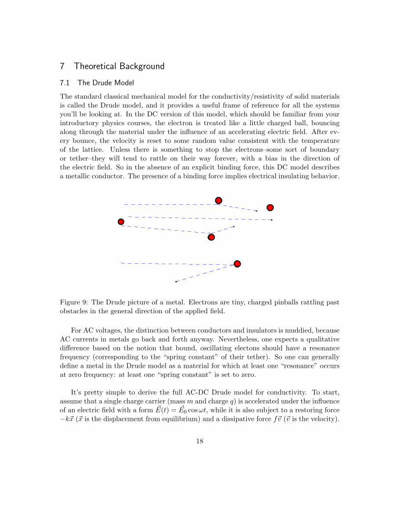
The standard classical mechanical model for the conductivity/resistivity of solid materialsis called the Drude model, and it provides a useful frame of reference for all the systemsyou’ll be looking at. In the DC version of this model, which should be familiar from yourintroductory physics courses, the electron is treated like a little charged ball, bouncingalong through the material under the influence of an accelerating electric field. After ev-ery bounce, the velocity is reset to some random value consistent with the temperatureof the lattice. Unless there is something to stop the electrons–some sort of boundaryor tether–they will tend to rattle on their way forever, with a bias in the direction ofthe electric field. So in the absence of an explicit binding force, this DC model describesa metallic conductor. The presence of a binding force implies electrical insulating behavior.
Figure 9: The Drude picture of a metal. Electrons are tiny, charged pinballs rattling pastobstacles in the general direction of the applied field.
For AC voltages, the distinction between conductors and insulators is muddied, becauseAC currents in metals go back and forth anyway. Nevertheless, one expects a qualitativedifference based on the notion that bound, oscillating electons should have a resonancefrequency (corresponding to the “spring constant” of their tether). So one can generallydefine a metal in the Drude model as a material for which at least one “resonance” occursat zero frequency: at least one “spring constant” is set to zero.
It’s pretty simple to derive the full AC-DC Drude model for conductivity. To start,assume that a single charge carrier (mass m and charge q) is accelerated under the influenceof an electric field with a form ~E(t) = ~E0 cosωt, while it is also subject to a restoring force−k~x (~x is the displacement from equilibrium) and a dissipative force f~v (~v is the velocity).
18
Solve the Newtonian ~F = m~a equation to find the amplitude and maximal speed of thesteady-state solution. Next note that the classical expression for the electrical currentdensity ~ is just ~ = nq~v, where n is the number density of the charges. One slick way tosolve the ~F = m~a equation is to rewrite the electric field as ~E(t) = ~E0e
iωt and take the realpart at the end of the calculation. This works because the equation of motion is linear.The answer is
~(t) =nq2 × iω
k −mω2 + ifω× ~E0e
iωt.
The proportionality between~ and ~E is the frequency-dependent electrical conductivityσ(ω). Its inverse is of course the electrical resistivity, ρ.
If you rationalize the denominator and take the real part of your answer, you will findthat it falls into two pieces: one part of the current is in phase with the electric field (goeslike cos(ωt)) and the other is π/2 out of phase (goes like sin(ωt)):
Re(~) =nq2ω2f
(k −mω2)2 + f2ω2× ~E0 cos(ωt)− nq2ω(k −mω2)
(k −mω2)2 + f2ω2× ~E0 sin(ωt).
What does this mean?
~ · ~E has the units of a power density. Over a cycle, the out-of-phase product sin cos av-erages to zero, but the in-phase cos2 averages to 1
2 . This nonzero part is the cycle-averagedpower transmitted to the current. Where does it go? Its proportionality to f is an impor-tant hint. Recall that f represents a damping force on a single oscillating charge. Whatwe have described here is a steady state: the kinetic energy of the current is dissipated bythe frictional force. By contrast, the out-of-phase part determines the energy flow into andout of the electromagnetic fields with no net loss.
Because we initially assumed k 6= 0, we have described a DC (ω = 0) insulator. Forω → 0, σ → 0 and ρ → ∞. However the same analysis goes through with k = 0, sothe expression for the conductivity for conductors is just the k = 0 limit of the generalexpression. This leads to another familiar interpretation of the dissipation coefficient f ina conductor. Given that the additional velocity of a charge accelerated in a DC field ~E fortime τ should be q ~Eτ/m, the current density should be
~DC =nq2 ~Eτ
m
(σDC =nq2τ
m).
19

Comparing this to the AC/DC formula we just derived with ω = 0, you’ll find thatf = m/τ . In other words, m/f is the average time for the uniform acceleration of anelectron by the external field, before the electron hits some obstacle and decays out of thecurrent.
1.0
Figure 10: The in-phase part of σ(ω) for a metal (k = 0). As f → 0 (τ →∞), the energyabsorption per cycle peaks more and more strongly about ω = 0.
7.2 “Perfect DC Conductors”
Things get a bit subtle when we try to imagine what would happen for a perfect DC con-ductor (k = 0 and f = 0 simultaneously). Imagine a sequence of graphs of the in-phasepart of the conductivity as τ → ∞ and f → 0. The typical Lorentzian narrows, and thepeak at ω = 0 simultaneously increases, in such a way that the total area under the curveremains constant. If we rescale the ordinate, we get closer and closer to what seems aperfectly thin spike at ω = 0. This f → 0 limit is a Dirac δ-function. For a perfect conduc-tor, with no dissipation, the in-phase conductivity happens at zero frequency. Because τrepresents the amount of time for which an electron retains the energy that the field givesit, and (for constant m) f → 0 makes τ →∞, a perfect conductor would be a great placeto store kinetic energy, transmit energy without loss, etc. If only life were that easy!
20

8 What affects the Resistivity
Here is where we start to talk about the effects that you can see with this apparatus.The Drude parameters n and τ turn out to have remarkable material- and temperature-dependences that tell a great deal about the physics of conductivity.
8.1 Impurity Scattering in Metals–a Surprising Temperature-Independence
The idea of perfect metallic conductivity is no relic of the Drude model. The quantummechanical treatment of the electron states in a lattice also implies that a single electronneed not scatter out of its momentum state. So why do metals exhibit finite τs? There aremany mechanisms to consider. The simplest to imagine is impurity scattering. An electricfield gives a directed momentum to a conduction electron. Classically, hitting somethingknocks it off-course. The quantum mechanical process is much the same. So we can getfairly far (though we can’t explain everything) by imagining a classical picture.
To be specific, consider the classical ballistic model for impurity scattering. Call thedensity of impurities Ni. Define the mean free path, Λ, as the length for which an electronon average hits one impurity. Actually, it’s easier to imagine the impurities sweeping towardthe charge carrier. Supposing that the radius of one impurity is ri, then Λ × πr2
iNi ∼ 1.But Λ = vτ , where v now stands for the average speed. So τ ∼ 1
vNi. This is true: the
dirtier the material, the higher the resistance. All else being constant, Ni → 0 impliesτ →∞.
For a fixed Ni, we might expect to be able to understand temperature dependencefrom the variation of v. If, as you might expect for a classical gas, v were something like√kBT/m (with kBT >> Eτ) then you might expect the impurity resistance to increase
with temperature. Why it doesn’t is due to the peculiarities of quantum mechanics.
Quantum mechanically, the electrons in a crystal are spread throughout the whole vol-ume. Imagine filling this space up to the appropriate electron density n. As you addelectrons, the quantum mechanical phenomenon of Pauli exclusion limits each state to twoelectrons. Suppose you put the first two electrons in the state of lowest kinetic energy, thatis, zero momentum. Newer electrons are forced into higher and higher momentum states.For a completely isotropic material, you’d end up with a Fermi ball of momentum states,filled out to the Fermi momentum pF .
On the other hand, you have a certain number N of electrons in a given crystal, andhowever you count, the number of occupied states has to be the same. Let’s count themomentum states and so relate N to pF . Using the uncertainty relation δxδpx ≈ h, withδx = Lx, the x dimension of the crystal, we get δpx ≈ h/Lx. Repeating for y and z, we
21

Ky
Kx
Fermi SurfaceState
Figure 11: Fermi Ball. The idea is that each momentum owns a particular volume ofmomentum space (specifically h3/V , where V is the volume of the sample). So the electrons,of which only two can ever have the same momentum, must stack up.
find that in momentum space, each state must take up a box of size ≈ h3/V . Filling states,two electrons per momentum, up to pF just gives twice the volume of the Fermi ball inunits of h3/V . Therefore
N = 2V ×43πp
3F
h3.
For macroscopic pieces of metal with Na atoms each with Z electrons, the number ofstates per unit volume per increment of momentum is 2 × h3/V , but the total number ofelectrons N = ZNa ∝ V . So you’ll always fill, say, a sample of nickel up to the same topmomentum. pF doesn’t change with the amount and can be treated as a property of thematerial.
In the absence of an electric field, the state of minimum energy requires that the Fermiball be centered around ~p = 0. With no electric field, if ~p is occupied, then so is −~p:everything is symmetric, and the total current = 0. But notice that on the electrons in theground state have an average kinetic energy of
〈KE〉0 =4π∫ pF0
p2
2mp2dp
43πp
3F
=3
5
p2F
2m.
Now suppose an electric force e ~E points to the right. The top states can move over to theright, then the states below those, and so on. . . until the entire ball has been shifted, pieceby piece, a bit to the right. There is now an average rightward momentum, the size ofwhich is limited by the effect of scattering: every so often, some of the rightward electronsare taken out of their right-going momentum state, and added onto the left side of the
22

Figure 12: Current-carrying state of the Fermi ball. The Fermi ball is displaced by theaverage momentum shift e ~Eτ . One electron has been scattered backwards, and another isgoing to hop into its place. The net current is density comes from the momentum statesin the crescent on the right.
23
Fermi ball. Some other electron gets accelerated into the newly vacant state.
In the equilibrium of the current carrying metal, the rightward acceleration and thescattering balance. The Fermi ball is built up on the right side and diminished on the leftside, but only to a point, so that it is approximately the same shape, just displaced by themomentum e ~Eτ . For reasonable current densities, this is much smaller than pF , so thelargest momentum of any single electron is still on the order of ~pF .
Hence the proper speed to use at all temperatures for which the metal is solid is theFermi speed, vF = pF /m, which for classical particles would correspond to a temperatureon the order of 104 to 105K. This is 10 − 100 times bigger than the melting point of anymetal. The fact that in metals the impurity resistivity is largely independent of temperatureis a consequence of the fact that electrons do not obey classical statistics.
There is another thing to notice here. You get a macroscopic current when the Fermiball is pushed one way, and the cancellation between ~p and −~p isn’t perfect. Now look atthe current density ~j the following way, as e/m×(the net momentum density). How muchnet momentum density is there in the situation where the Fermi ball is displaced by e ~Eτ?Let AF stand for the surface area of the Fermi ball. If e ~Eτ pF , then the net momentumdensity due of all of the occupied states will be the momentum density of the states in theuncancelled crescent, about
〈~p〉V
= 2pF3h3×AF e ~Eτ,
(2 for the spins and the factor of 1/3 because we are displacing in the x direction only)and
~j = 2pF3h3×AF e2 ~Eτ/m.
This means that in the quantum mechanical theory of metals, n = 2pF /3h3 × AF =
83πp
3F /h
3. But because we filled states up to pF , this is just N/V . So the Fermi ball ideasreturn the simple Drude n.
8.2 Phonon Scattering in Metals: Varying τ with Temperature
Faced with the multiplicity of scattering mechanisms, you might not be surprised that thegeneral computation of the electrical resistivity of a metal can turn into a very complicatedundertaking. The total scattering rate should be something like the sum of all the differentrates taken individually. That is, 1
τtotal= 1
τimpurity+ 1
τother. 4 But there is some hope of
4In other words, all else being constant, the various resistivities of the material should add like resistorsin series.
24

disentangling the major contributions because each mechanism has a characteristic tem-perature dependence.
In the Bloch-Gruneisen model of metallic conductivity, the two major process is scat-tering from lattice distortions. In the harmonic theory of crystal structure, such distortionsare made up of phonons–vibrational modes of the lattice. A lucky confluence of phononswill cause local variations in the lattice density that act like scattering centers. Bloch andGruneisen focused on two features of phonons:
1. Phonons carry momentum. Electrons “scatter” from phonons by absorbing or emit-ting phonons. So a given phonon scatters a given current-carrying momentum stateto a definite destination. So different phonons will be more or less effective at reducingthe current, depending on their momenta.
2. The number density of phonons of a given energy (and hence momentum) changeswith temperature. So unlike impurity scattering, phonon scattering will be temper-ature dependent.
The first feature implies a geometry problem. Because phonons energies are relativelylow compared to p2
F /2m, we only have to consider scattering of electrons near the surfaceof the displaced Fermi ball (the Fermi surface)–we haven’t go the necessary energy topromote an electron from deep inside. The elastic scattering of an electron at the FermiSurface from a phonon of momentum ~q leads to a loss of momentum (as measured fromthe current direction)
∆p = pF (1− cos θ)
and this loss can be averaged over the Fermi surface to get the net effect for that particular~q:
< ∆p >Surface= 2πpF
∫ θMax
0n(θ)(1− cos θ) sin θdθ,
where n(θ) is the number density of phonons available for scattering electrons through theangle θ. θMax corresponds to the largest possible scattering angle–obviously belonging tothe largest possible ~q.
The second feature brings in statistical mechanics. The scattering is geometricallylimited to sin(θ/2) < q/2pF . So the question is: what’s the typical q at a temperature T?This depends on both the number of phonons of a given energy, and the dependence of qon the energy of the phonon. Since phonons are Bose particles, their occupation numberas a function of temperature is
nq ∼1
eEq/kBT − 1∼ kBT/Eq
25
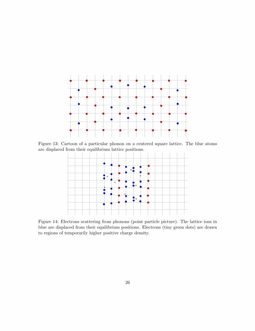
Figure 13: Cartoon of a particular phonon on a centered square lattice. The blue atomsare displaced from their equilibrium lattice positions.
Figure 14: Electrons scattering from phonons (point particle picture). The lattice ions inblue are displaced from their equilibrium positions. Electrons (tiny green dots) are drawnto regions of temporarily higher positive charge density.
26

KfKfFermi Surface
q
Figure 15: Phonon scattering cartoon (momentum space version). Here q is the phononmomentum and the initial and final electron states are taken to be on the Fermi surface.
with the last expression as a very crude approximation for phonons of energy E(q) andmomentum q.
For the relation between q and Eq, there is the Debye model. In the Debye model, theenergy of a phonon of momentum q is just cq, where c is the speed of sound in the crystal,and (as with light) q is h/λ. The sound modes have a natural largest momentum qD (“D”for Debye) corresponding to the inverse dimensions of a cell of the crystal, with a largestenergy ED = cqD. By dividing ED/kB, we convert ED to the Debye temperature, ΘD.So to find the typical 〈q〉T at typical energy kBT , we may estimate its momentum as afraction of qD by simple proportionality: q/qD = E/ED → 〈q〉T = qD(T/ΘD).
As with electron states, each distinct phonon momentum takes up h3/V of momentumspace. There are Na atoms in the crystal, and 3 ways for each atom to move, which leads to3Na different possible phonon states (as compared to ZNa electron states). Hence we canbuild a Debye ball in much the same way we built up a Fermi ball. The difference is thateach phonon momentum state can be occupied by many more than two phonons, becausephonons are Bose particles. But because the radius of the Fermi ball (∼ (ZNa)
13 ) will be
comparable to the radius of the Debye ball (∼ (3Na)13 ), qD and pF are around the same size.
For temperatures T ΘD, the shorter wavelength, higher energy phonons “freezeout”: they become much rarer than their low-energy, longer-wavelength, and hence smallerq cousins. Using the fact that the maximum phonon momentum, qD, is about the same aspF we take the typical phonon 〈q〉 to be much smaller than pF . So at low temperatures, wecan (again, very crudely) approximate q/pF ∼ θ. Retaining the crude approximation thatthe number of these surviving low-energy phonons is proportional to T , you can calculate
27

that:
< ∆p >Surface∝ 2πpFT
∫ T/ΘD×qD/pF
0(1− cos θ) sin θdθ ∝ T 5.
The connection to a Drude parameter is that the rate of momentum loss from the cur-rent is proportional to 1/τ . So the above expression says that at low temperatures, as thehigher energy phonons freeze out, the resistance vanishes very quickly. At high tempera-tures, the upper limit of the integral saturates at qD/pF , so the temperature dependencefor T > ΘD will be linear.
A more careful calculation along the same lines yields the Bloch-Gruneisen formula
1
τ= vFσa
h2q2DkB
Mak2BΘD
(T
ΘD
)5 ∫ ΘD/T
0
4z5dz
(ez − 1)(1− e−z).
Ignore for now the jumble of constants5, and realize that what’s left is a universal functionof T/ΘD. So this theory says that, for any metal whatsoever, if you plot temperature inunits of ΘD, and resistance in units of the resistance at ΘD, then the R-T graphs of allmetals will look exactly the same. That’s a big prediction! Though not perfectly correct,this simple Bloch-Gruneisen model works remarkably well for a variety of metals, and youwill clearly see the effects of the phonons freezing out in the R-T curve for your platinumsample.
8.3 Band Gaps: Varying n with Temperature
In the Drude picture of an insulator, to generate a DC conductivity, you have to break thesprings that tether some number of electrons to their nuclei. To free a charge requires anactivation energy–but once the charge is free, it can wander around under the influence ofan electric field, almost as if it were in a metal. As the temperature increases, one expectsa population of thermally excited carriers. Recall that the Drude-model conductivity σ =nq2τm . We saw above that the number of electrons at energy ε follows the Fermi distribution–
they stack up into higher energy states when they are made to encounter each other often.But because insulators are, well, insulating at room temperature, we would expect thatthe number of free electrons should be small, making electron-electron collisions unlikely.So in an insulator the freed electrons approximate a Maxwell-Boltzmann gas. For theproportion of electrons available to conduct at temperature T , with a tethering energy G,we’d calculate
n ∝∫ ∞
0e−(p2/2m+G)/kBT × 4πp2dp
h3∝ T 3/2e−G/kBT .
5σa is the cross section for scattering from a single atom, and will be an important thing to know aboutwhen you try to understand what might change at the Curie point in nickel. To understand where theother constants come from, consult the references and/or your lab instructor.
28
A semiconductor is just an insulator with a smallish G, so that at room temperature it willconduct electricity, but at low temperature, it insulates. The difference between crystallineinsulators and semiconductors is one of degree, rather than kind.
Of course quantum mechanics modifies the Drude picture. To see how, consider thecase of a strongly bonded insulator like diamond. In the ideal diamond lattice, each carbonatom shares its outer four n = 2 electrons with four other carbon atoms, in four covalentbonds. There is no saying which carbon atom any of these bonding electrons belong to–infact, these electrons must live in states that extend throughout the crystal.
As you saw for the case of a metal with extended states, the net electric current isreally the effect of a disproportionation in the occupancy of momentum states–e.g., morerightward than leftward states, and the displacement of the Fermi ball. So in an insula-tor, something must happen to stop the disproportionation. The cause is called a band gap.
The band gap is a purely quantum mechanical effect. First, imagine graphing theenergy as a function of momentum for an electron. For a free electron, you’d expect thesmooth parabola E = p2/2m–and this is what I used in describing a metal. But thiscan only have been a great approximation. As you know from optics, a wave movingover a lattice generates reflections which can interfere with the original wave. And youhave probably heard of the DeBroglie relationship between wavelength and momentum,λ = h/p. Now when, in the case of electrons moving through a lattice of ions, λ isabout twice the separation between adjacent atoms, the reflecton leads to something likea standing wave on a string. The probability density of finding a charge piles up in oneof two patterns–either in the region between the nuclei, or right atop the ions. Becauseof the Coulomb interaction, the energy of the electron state in each case is different. Butsince the momentum for each state is the same, there will be a discontinuous jump in theallowed energy. There is a band of allowed energies below the critical momentum, andanother band of allowed energies above the critical momentum. The band gap is just thisforbidden range of energies.
Now imagine filling up the states with electrons, just as in a metal. With the rightnumber of electrons, you can fill states right up to the edge of the gap. In a partially emptyband, there are empty states of nearly the same energy allowing the electrons in the toplevels to gain small increments of momentum. If the band is filled, there are no nearbystates–an electron at the top level of a filled energy band must gain a finite amount ofenergy to change its momentum. So a crystal with filled bands is an insulator. The filled,lower bands are called valence bands, while the upper, empty bands are called conductionbands.
29

Figure 16: A schematic of the energy bands in a crystalline solid.
8.4 Conduction Electrons, Valence Holes, ∆, and Doping
When an electron does acquire enough energy to jump the gap and provide current, itleaves behind a vacant state called a hole. This valence hole provides another place foran electron in the valence band to go–but when it does, it leaves behind its own vacancy.In effect, when the valence electron filled the valence hole, the hole moves in the oppositedirection. So when an electron jumps from the valence band to the conduction band, twocharge carriers are made: an electron-hole pair. Of course, a conduction electron can alsofill a valence hole in the reverse process.
In equilibrium, the rate of collisions between conduction electrons and valence holesshould match the rate of spontaneous pair creation:
nenh ∝ e−∆/kBT .
In a pure insulator, the only way to get conduction electrons is pair creation, so the densitiesof electrons and holes are equal: ne = nh. Hence for a pure semiconductor
ne ∝ e−∆/2kBT .
But very pure semiconductors are quite hard to make. Crystals are easily contaminatedwith impurities of different atoms or contain lattice imperfections that can either contributean electron to the conduction band or create a valence hole, and this makes a direct mea-surement of the band gap ∆ difficult. But there is a workaround, using semiconductors
30
intentionally doped with a comparatively large concentration of impurities. To understandhow this works, you first need a sketch of how doping systematically changes the electronand hole densities in semiconductors.
A crystal of Si (valence 4) doped with P (valence 5) will have a surplus of conductionelectrons. Such n-type dopants contribute filled electron states near the top of the energygap, which are easily excited into the conduction band. But the holes they leave behind arelocalized near the dopant and so do not conduct. An n-type semiconductor has many moreconduction electrons than valence holes. The majority carriers in an n-type semiconductorare electrons.
On the other hand Al (valence 3) dopants in Si contribute holes (the lack of an electron)near the bottom of the gap, just above the top of the valence band. Electrons from thetop of the valence band easily jump into these vacant states, where they become localizedaround the impurity, and leave behind a mobile valence hole. Thus p-type semiconductorshave more valence holes than conduction electrons. The majority carriers in a p-type semi-conductor are holes.
At most temperatures, the number of carriers contributed by dopants far exceeds thenumber of intrinsically excited carriers. Hence in n-type Si, for example,
ne = nd + nh,
but the same rate equation still applies, so that
nenh = (nd + nh)nh ∝ e−∆/kBT → nh ∝ e−∆/kBT
when nd nh. So to measure ∆, you can measure the minority carrier density (nh in ann-type material or ne in a p-type material). This is much easier and much less expensivethan growing ultrapure crystals.
8.5 The Diode
You will be measuring the minority carrier current I0 in a device called a junction diode.This consists of a single piece of doped semiconductor, in which the doping changes fairlyabruptly from n-type to p-type: for this reason it is also called an “np junction”. Of coursea “pn junction” would also be an accurate name for it.
When the junction is formed, loosely bound dopant carriers from each side wander overthe boundary, where they tend to become trapped: doped electrons from the n-type sidewill fall into the extra electron states provided by the p-type dopants on the p side, andextra holes from the p-type side will sit in the extra empty states provided by the n-type
31

Figure 17: The basic ideas of of (top) n doping and (bottom) p doping.
32

dopants on the n side. So when the junction is formed, the n side acquires a net positivecharge, and the p side a quires a net negative charge. Once equilibrium is established, thereis a potential boundary V0 to the further flow of majority carriers: holes from the p side tothe n side, and electrons from the n side to the p side. In terms of the energy bands, onesays that across the junction, the energy levels of the electron states are “bent,” or shiftedacross the junction. Calling the absolute magnitude of the electron or hole charge q, themagnitude of the shift is qV0.
Figure 18: Band bending across an np junction.
In equilibrium, there is no net current flow across the np junction. Yet at any nonzerotemperature, there will be minority carriers–holes on the n side and electrons on the p side–which would easily slide downhill. Call this minority leakage current I0. It is composed ofthermally generated charge carriers, so
I0 = C0e−∆/kBT ,
where C0 has to do with the conductivity of the minority carriers and the strength of thespontaneous electric field across the junction (if d0 is the thickness of the junction, thenC0 should be proportional to V0/d0 × τq2/m). But no net current flows in equilibrium. I0
is cancelled by the small current of majority carriers that have enough thermal energy toget over the potential barrier:
IM (0) = CMe−qV0/kBT = I0.
33
where CM depends on the majority carrier τ and m (which could be different).
Now the way a diode works is that, if you apply a voltage Va which lowers the potentialbarrier from qV0 to qV0 − qVa, you exponentially increase the majority current flow:
IM (Va)/IM (0) = IM (Va)/I0 = eqVa/kBT ,
so thatIM (Va) = I0e
qVa/kBT .
If you reverse the polarity of Va to augment the barrier, you exponentially decrease themajority current flow. So the diode acts like a one-way (non linear) conductor for majoritycarriers. Calling the direction of majority current flow “positive”, the total current is then
IT (Va) = IM (Va)− I0 = I0(eqVa/kBT − 1) = C0e−∆/kBT (eqVa/kBT − 1).
This model is good as long as Va is not too big compared to V0. For fixed temperature,you can step through different currents and trace out the I versus Va curve, and fit for I0.After doing this for several temperatures, you can extract ∆ (and C0) from a logarithmicplot of I0 against 1/kBT .
8.6 A Constant-Current Measurement Scheme
A different way to extract ∆ uses the particular strength of your apparatus, that electricalmeasurements are based on a controlled current source. If you plot several V-I curves onthe same set of axes, you will see that they are all, approximately, shifted copies of thesame shape. Now suppose you look at large enough currents that you can ignore the −1as compared to the exponential. Then for a given temperature and applied voltage, thecurrent is
I(T, Va) ∝ eqVa−∆kBT .
For two different temperatures, T and T ′, the same current happens at different appliedvoltages Va and V ′a:
I(T, Va)
I(T ′, V ′a)= 1 = e
qV a−∆kBT
− qV ′a−∆
kBT ′ ,
in other words,
∆ = qVaT
′ − V ′aTT ′ − T
.
This might be an easier way to extract ∆ from a series of measurements at constant current,as it avoids the difficulties of curve-fitting.
34

8.7 τ for a Semiconductor
You will be trying to measure ∆ by ascribing the temperature dependence of the minoritycarrier current I0 to the minority carrier concentration. You might worry whether it’s safeto ignore the temperature dependence of τ .
The impurity scattering time for a semiconductor does depend on temperature, thoughnot nearly as strongly as the minority carrier concentration. Here is one way to graspthe main result. For a Maxwell-Boltzmann gas, the thermal wavelength corresponding tokinetic energy 1
2kBT of each quantum mechanical particle (of mass m) is
λT =
√h2
2mkBT.
This defines a temperature-dependent volume VT per particle of λ3T ∼ (kBT )−3/2. Now
NiVT will be the number of scatterers in the same volume, so you would expect that forthe impurity scattering rate, 1/τi ∝ (kBT )−3/2, and τ ∝ (kBT )3/2.
The reason the analysis of the impurity scattering time for semconductors differs fromthat in metals is that for metals, the charge density n is much larger (on the order of oneelectron per unit cell) and basically independent of T . Maxwell-Boltzmann statistics areno longer a good approximation, and the appropriate temperature to use for the “thermalwavelength” would be the Fermi temperature TF (typically TF ∼ 104K), which is propor-tional to n2/3. In other words, the average spread of the charge carrier wavepackets ismetals about a lattice constant–much smaller than the typical impurity spacing–and so inmetals the ballistic approach works better.
And what about the phonon scattering? If we were to repeat the same sort of anal-ysis that we made for phonon scattering in a metal, the big difference would be that thenumber of electrons is smaller than for a metal. At room temperature or lower, the Fermiball would be much smaller–and hence the geometric restriction, which is the source ofthe strong temperature dependence when the phonons freeze out, would no longer be inforce. So phonon scattering in insulators has a comparatively weak temperature depen-dence, probably more like the Bloch-Gruneisen formula for high temperatures, ie 1/τph ∝ T .
So for the total τ , we’d expect
1
τ=
1
τi+
1
τph= aT−
32 + bT ,
and so
ρ ∝ 1
nτ∝ e∆/kBT × (aT−3 + bT−
12 ).
35

To extract ∆ from a measurement of σ, you would write this as a function of β = 1/kBT ,and consider the logarithm:
lnσ = − ln ρ = −∆β + . . .+ constants.
The . . . terms are on the order of lnβ, and these are the ones you are thinking of ignoring.The rate of change of lnβ = 1/β = kBT . Compare this to the linear coefficient ∆: at“low” temperatures, kBT/∆ 1, and only the strong exponential temperature depen-dence matters when measuring σ. So you can ignore lnβ terms for “low” temperatures.Using kB ≈ 1.38× 10⁻²³J/K and 1eV ≈ 1.602× 10⁻¹⁹J , 1eV ↔ 1.16× 10⁴K. Therefore,for band gaps on the order of 1eV , “low temperature” is well below the melting point ofthe typical solid.
8.8 Band Gap Temperature Dependence?
If you take a more careful look at the theoretical considerations which lead to the bandstructure of a solid and the gaps between bands, it becomes apparent that the size of theband gaps depend on the separations between adjacent atoms of the lattice. Because thelattice parameters change slowly as a function of temperature, the band gap itself will vary.Experimentally, the band gaps of Si and Ge (the most common semiconductors for diodes)vary by around 10% between room temperature and 100K. The general decrease in bandgap as temperature increases is consistent with the idea that the interactions that underlythe band structure decrease as the lattice thermally expands.
Under the assumption that the temperature dependence of ∆ is gradual, but stillstronger than the temperature dependence of the mobility, you could use the constant-current measurement scheme to estimate ∆(T ).
9 Electronic Phase Transitions
Having seen ice melt and water turn to steam, you are familiar with the notion of phasetransitions. In the case of water, the chemical identity of the molecules stays the same, butthey occupy space and interact very differently with one another in the distinct physicalphases. Often, you hear of these in a hierarchy: “solid, liquid, gas,” or “gas, liquid, solid.”In going one way or the other through the list, you notice that water vapor is rarefied, themolecules weakly interacting to the point that a gas will expand to fill whatever containerit’s in. Liquid water is shapeless, but the molecules draw on each other enough that thefluid has a definite volume. And ice has a definite shape–the interactions in ice are surelythe strongest.
36
A similar thing can happen with the electrons in a solid. You might think of the solidas defining the available space, and (for most, but not all, phase transitions) the electronsas the analogue of the water molecules. Some electrons, by interacting with each other,often by an intermediary such as the motions of the lattice, change in phase from an un-correlated “gas,” to a much more correlated, more “condensed” substance–something moreakin to a liquid or solid. Since the electrons are responsible for the electrical conductivity,the phase transition often has a definite signature in the resistivity measurement. Here aretwo electronic phase changes that you can investigate.
9.1 Itenerant Ferromagnetism in Nickel: Changing σa
At room temperature, a piece of nickel metal is magnetic. The magnetization m is therelative difference between the densities of oppositely polarized spins. Below a Curie-Weisstemperature TC , the spins of the electronic magnets tend to align with each other. Butmagnetic nickel is also a metal–in fact, most well-known magnets are also metals. Being ametal requires conduction electrons. These of course bounce around through the metal.
The question is, then, with all of this bouncing around, how the electrons in a mag-net maintain their polarization–and whether the polarized ones are even the same as theconducting ones. It turns out that in magnetic nickel, the conduction electrons are indeedpolarized. There is a model, due to Stoner, which explains how this can occur, and thesame ideas have consequences for the resistivity.
In lone atoms of some d-series metals like nickel, the d electrons tend to align with oneanother. In a piece of nickel metal, the itinerant electrons may interact when two of themoccupy d states on the same nickel atom, one right after the other. In that case there wouldbe a large effective force causing the spins to align–it is energetically favorable for them todo so. Two such electrons, in mutual agreement, may go on their way, and interact withother nickel atoms. On the other hand, two oppositely polarized electrons will not be ableto go through the same nickel at nearly the same time, and the second electron will insteadbe deflected. In other words, consider the effective scattering cross section for the secondelection to pass through a given nickel atom. If the first and second electron are polarizedparallel to each other, you expect one cross section, σ↑↑ = σ↓↓. If they are oppositely po-larized, you expect a different cross section, σ↑↓. The second scattering process is stronger:σ↑↓ > σ↑↑.
But all of the electrons have to hop from nickel to nickel–there’s no other way to getaround. In an environment where the majority of the electrons are already polarized inthe same direction, it costs energy to point the other way. In Stoner’s model, TC is thetemperature at which this extra energy becomes scarce enough that the polarization inter-
37

actions dominate. Which polarization gets the upper hand is a matter of chance, but once asufficiently large local fluctuation happens to polarize enough electrons one way, the wholepiece of nickel goes over. There will be the occasional “wrongly polarized” electron, butthey don’t last for long in any one place. At lower temperatures, deeper into the magneticstate, the free energy scarcity worsens, and the number of electrons that have the “wrong”polarization become ever rarer.
In the Bloch-Gruneisen picture, the resistivity is proportional to σa, which is the averagecross section for scattering by a single atom: the size of σa determines the high-temperatureslope of the resistance versus temperature graph. From the above argument, this willchange as the conduction electrons get polarized. As the temperature decreases belowTC , you would expect the resistance to drop below the trend for T > TC , because as themagnetism sets in, polarization mismatches should become ever more rare. Right at TC ,there ought to be a kink in the resistance versus temperature curve as the cooperative effectsuddenly kicks in. To see this, consider the rate of encounters between ↑ and ↓ electronson the same nickel atom. The scattering rates will be proportional to
σ↑↑n2↑
2+ σ↓↓
n2↓
2+ σ↑↓n↑n↓,
since n↓+n↑ = n, and n↑−n↓ is the magneization m, and since σ↑↑ = σ↓↓, this expressioncan be rewritten as
σ↑↑n2 + m2
4+ σ↑↓n
2 −m2
4,
so the change in the resistivity due to m should be proportional to
m2 (σ↑↑ − σ↑↓)4
.
Hence by measuring the “missing resistance” (the discrepancy between the resistancepredicted by the T > TC trend and the actual T < TC resistance), you can estimate |m|as a function of temperature.
9.2 Superconductivity: More than τ →∞
While the idea of perfect metallic conductivity is understandable within the context ofthe Drude model for independent electrons, superconductivity (which by contrast is anactually attainable state) is not. While normal currents in a metal decay by scattering,for supercurrents there is an energy gap–analogous to the band-gap that makes insulatorswork–which means that scattering itself requires energetic activation. Hence materials inthe superconducting state are qualitatively different from merely excellent regular conduc-tors.
38
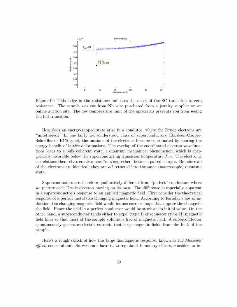
5 10 15 20 25 30
2.3
2.35
2.4
2.45
2.5
2.55
2.6
2.65
x 10!5
X: 8.909Y: 2.473e!005
Temperature (K)
Res
ista
nce
(!)
Nb from Ebay
TSC" 9K
Figure 19: This ledge in the resistance indicates the onset of the SC transition to zeroresistance. The sample was cut from Nb wire purchased from a jewelry supplier on anonline auction site. The low temperature limit of the apparatus prevents you from seeingthe full transition.
How does an energy-gapped state arise in a condutor, where the Drude electrons are“untethered?” In one fairly well-understood class of superconductors (Bardeen-Cooper-Schreiffer or BCS-type), the motions of the electrons become coordinated by sharing theenergy benefit of lattice deformations. The overlap of the coordinated electron wavefunc-tions leads to a bulk coherent state, a quantum mechanical phenomenon, which is ener-getically favorable below the superconducting transition temperature TSC . The electroniccorrelations themselves create a new “moving tether” between paired charges. But since allof the electrons are identical, they are all tethered into the same (macroscopic) quantumstate.
Superconductors are therefore qualitatively different from “perfect” conductors wherewe picture each Drude electron moving on its own. The difference is especially apparentin a superconductor’s response to an applied magnetic field. First consider the theoreticalresponse of a perfect metal to a changing magnetic field. According to Faraday’s law of in-duction, the changing magnetic field would induce current loops that oppose the change inthe field. Hence the field in a perfect conductor would be stuck at its initial value. On theother hand, a superconductor tends either to expel (type I) or sequester (type II) magneticfield lines so that most of the sample volume is free of magnetic field. A superconductorspontaneously generates electric currents that keep magnetic fields from the bulk of thesample.
Here’s a rough sketch of how this large diamagnetic response, known as the Meissnereffect, comes about. So we don’t have to worry about boundary effects, consider an in-
39
finitely long, thick slab of superconductor. It is always tempting to think of electrons likelittle balls of charge, with velocity ~v, such that ~j = ne < ~v >. But to construct a localizedparticle out of waves requires a particular sum of momentum states. Superconductivitydepends explicitly on the correlated multi-electron wavefunction, and this single-particlepicture breaks down: the momentum states are added up in a very different way. Becauseof the energy gap between this ground state and the single-particle-like excitations, theapplied vector potential can’t change the shape of the wavefunction by much.
It seems paradoxical that current can both flow and not flow in the “ground” state,depending on whether we are applying a magnetic field. The resolution to this paradoxresides in the difference between the < m~v >-momentum of a localized particle and thecanonical momentum −ih∇ in the Hamiltonian. In the presence of a vector potential ~A,the operator for m~v is modified from −ih∇ to −ih(∇− e ~A/c). Since the ∇ operator de-scribes the shape of the wavefunction in space–which can’t change because of the energygap–the expectation value of current < ne~v > must be proportional to < −ne2 ~A/mc >.So the vector potential acts as a direct push on the totality of “particles” that comprise thesuperconducting state, resulting in something like a Galilean translation of a rigid solid.By applying the appropriate Maxwell’s equations, you will find that this supercurrent ex-ponentially screens out a magnetic field.
Superconductivity was first discovered in solid mercury by Heike Kammerleigh Onnesin 1911, soon after he had succeeded in the liquefaction of helium. Superconducting wireswith the ability to carry large currents are used in the production of the very strongcryogenic electromagnets used in diagnostic NMR machines. In the 1980’s, Bednorz andMuller discovered superconductivity at the relatively high temperature of 35 K in a layeredcopper-oxide. As part of this lab, you have the opportunity to make (or, if time doesn’tpermit, at least measure) a similarly structured compound that becomes superconductinganywhere from 70 − 90 K, depending on the details of how you produce it. Althoughthe recipe for making this material is well known, there is as yet no consensus about theinteraction which makes its superconducting transition occur.
10 Theory References
• Professor Y.J. Uemura’s Condensed Matter Lectures, at http://www.columbia.edu/~yu2/.
• The Solid State: From Superconductors to Superalloys, Andre Guinier andRemi Jullien, pp. 74–120 (fundamentals of electrical conductivity), 144-156 (ferro-magnetism).
• Principles of Solid State Physics, J.M. Ziman, chapter 2 (phonons), chapter 7
40

(transport properties), chapter 10 (magnetism) and chapter 11 (superconductivity).
• The Feynman Lectures on Physics, vol. III, R.P. Feynman, chapter 13 (onthe electron states in a crystal lattice), chapter 14 (semiconductors), and chapter 21(superconductivity).
41