Circuit Note - Digi-Key Sheets/Analog Devic… · · 2014-08-19Circuit Note CN-0325 ... S1 S2 S3...
11
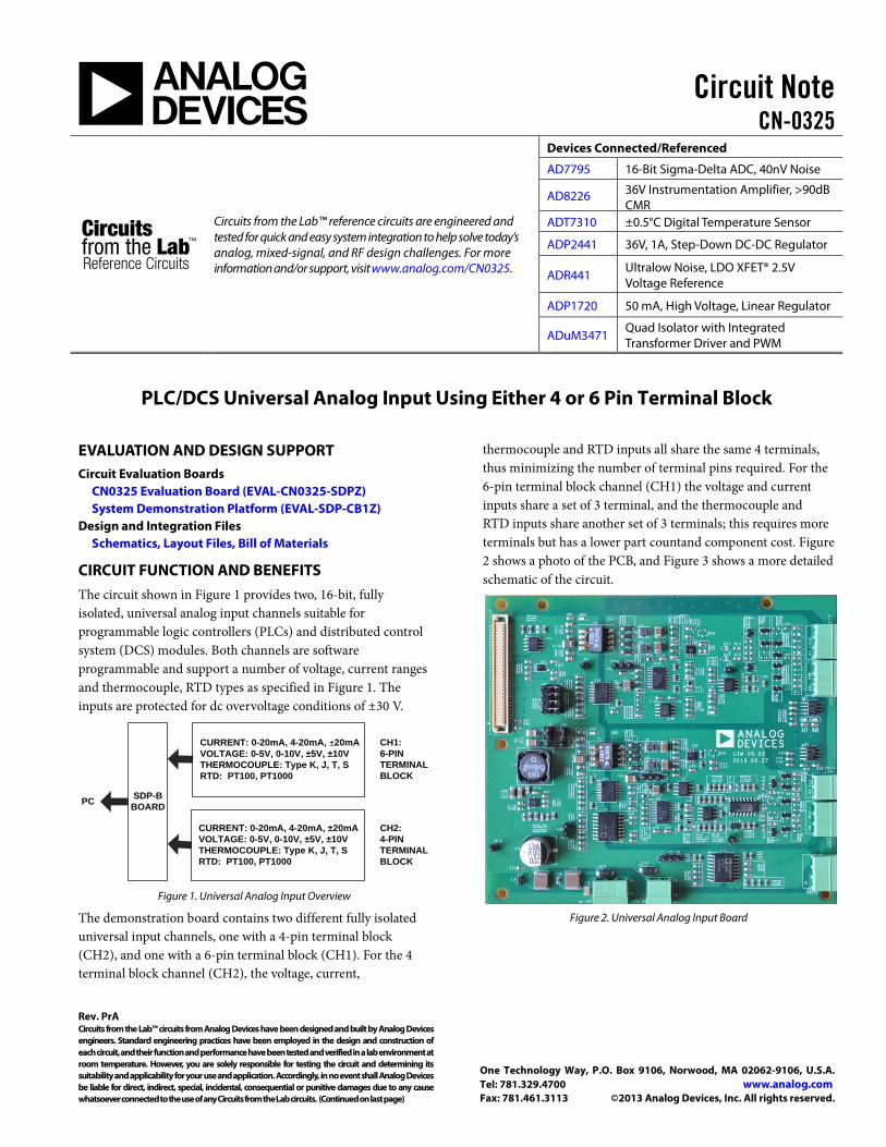
Circuit Note CN-0325 Circuits from the Lab™ reference circuits are engineered and tested for quick and easy system integration to help solve today’s analog, mixed-signal, and RF design challenges. For more information and/or support, visit www.analog.com/CN0325. Devices Connected/Referenced AD7795 16-Bit Sigma-Delta ADC, 40nV Noise AD8226 36V Instrumentation Amplifier, >90dB CMR ADT7310 ±0.5°C Digital Temperature Sensor ADP2441 36V, 1A, Step-Down DC-DC Regulator ADR441 Ultralow Noise, LDO XFET® 2.5V Voltage Reference ADP1720 50 mA, High Voltage, Linear Regulator ADuM3471 Quad Isolator with Integrated Transformer Driver and PWM PLC/DCS Universal Analog Input Using Either 4 or 6 Pin Terminal Block Rev. PrA Circuits from the Lab™ circuits from Analog Devices have been designed and built by Analog Devices engineers. Standard engineering practices have been employed in the design and construction of each circuit, and their function and performance have been tested and verified in a lab environment at room temperature. However, you are solely responsible for testing the circuit and determining its suitability and appl icability for your use and application. Accordingly, in no event shall Analog Devices be liable for direct, indirect, special, incidental, consequential or punitive damages due to any cause whatsoever connected to the use of any Circuits from the Lab circuits. (Continued on last page) One Technology Way, P.O. Box 9106, Norwood, MA 02062-9106, U.S.A. Tel: 781.329.4700 www.analog.com Fax: 781.461.3113 ©2013 Analog Devices, Inc. All rights reserved. EVALUATION AND DESIGN SUPPORT Circuit Evaluation Boards CN0325 Evaluation Board (EVAL-CN0325-SDPZ) System Demonstration Platform (EVAL-SDP-CB1Z) Design and Integration Files Schematics, Layout Files, Bill of Materials CIRCUIT FUNCTION AND BENEFITS The circuit shown in Figure 1 provides two, 16-bit, fully isolated, universal analog input channels suitable for programmable logic controllers (PLCs) and distributed control system (DCS) modules. Both channels are software programmable and support a number of voltage, current ranges and thermocouple, RTD types as specified in Figure 1. The inputs are protected for dc overvoltage conditions of ±30 V. Figure 1. Universal Analog Input Overview The demonstration board contains two different fully isolated universal input channels, one with a 4-pin terminal block (CH2), and one with a 6-pin terminal block (CH1). For the 4 terminal block channel (CH2), the voltage, current, thermocouple and RTD inputs all share the same 4 terminals, thus minimizing the number of terminal pins required. For the 6-pin terminal block channel (CH1) the voltage and current inputs share a set of 3 terminal, and the thermocouple and RTD inputs share another set of 3 terminals; this requires more terminals but has a lower part countand component cost. Figure 2 shows a photo of the PCB, and Figure 3 shows a more detailed schematic of the circuit. Figure 2. Universal Analog Input Board SDP-B BOARD CURRENT: 0-20mA, 4-20mA, ±20mA VOLTAGE: 0-5V, 0-10V, ±5V, ±10V THERMOCOUPLE: Type K, J, T, S RTD: PT100, PT1000 CURRENT: 0-20mA, 4-20mA, ±20mA VOLTAGE: 0-5V, 0-10V, ±5V, ±10V THERMOCOUPLE: Type K, J, T, S RTD: PT100, PT1000 CH1: 6-PIN TERMINAL BLOCK CH2: 4-PIN TERMINAL BLOCK PC
Transcript of Circuit Note - Digi-Key Sheets/Analog Devic… · · 2014-08-19Circuit Note CN-0325 ... S1 S2 S3...
Circuit Note CN-0325
Circuits from the Lab™ reference circuits are engineered and tested for quick and easy system integration to help solve today’s analog, mixed-signal, and RF design challenges. For more information and/or support, visit www.analog.com/CN0325.
Devices Connected/Referenced
AD7795 16-Bit Sigma-Delta ADC, 40nV Noise
AD8226 36V Instrumentation Amplifier, >90dB CMR
ADT7310 ±0.5°C Digital Temperature Sensor
ADP2441 36V, 1A, Step-Down DC-DC Regulator
ADR441 Ultralow Noise, LDO XFET® 2.5V Voltage Reference
ADP1720 50 mA, High Voltage, Linear Regulator
ADuM3471 Quad Isolator with Integrated Transformer Driver and PWM
PLC/DCS Universal Analog Input Using Either 4 or 6 Pin Terminal Block
Rev. PrA Circuits from the Lab™ circuits from Analog Devices have been designed and built by Analog Devices engineers. Standard engineering practices have been employed in the design and construction of each circuit, and their function and performance have been tested and verified in a lab environment at room temperature. However, you are solely responsible for testing the circuit and determining its suitability and applicability for your use and application. Accordingly, in no event shall Analog Devices be liable for direct, indirect, special, incidental, consequential or punitive damages due to any cause whatsoever connected to the use of any Circuits from the Lab circuits. (Continued on last page)
One Technology Way, P.O. Box 9106, Norwood, MA 02062-9106, U.S.A. Tel: 781.329.4700 www.analog.com Fax: 781.461.3113 ©2013 Analog Devices, Inc. All rights reserved.
EVALUATION AND DESIGN SUPPORT Circuit Evaluation Boards
CN0325 Evaluation Board (EVAL-CN0325-SDPZ) System Demonstration Platform (EVAL-SDP-CB1Z)
Design and Integration Files Schematics, Layout Files, Bill of Materials
CIRCUIT FUNCTION AND BENEFITS The circuit shown in Figure 1 provides two, 16-bit, fully isolated, universal analog input channels suitable for programmable logic controllers (PLCs) and distributed control system (DCS) modules. Both channels are software programmable and support a number of voltage, current ranges and thermocouple, RTD types as specified in Figure 1. The inputs are protected for dc overvoltage conditions of ±30 V.
Figure 1. Universal Analog Input Overview
The demonstration board contains two different fully isolated universal input channels, one with a 4-pin terminal block (CH2), and one with a 6-pin terminal block (CH1). For the 4 terminal block channel (CH2), the voltage, current,
thermocouple and RTD inputs all share the same 4 terminals, thus minimizing the number of terminal pins required. For the 6-pin terminal block channel (CH1) the voltage and current inputs share a set of 3 terminal, and the thermocouple and RTD inputs share another set of 3 terminals; this requires more terminals but has a lower part countand component cost. Figure 2 shows a photo of the PCB, and Figure 3 shows a more detailed schematic of the circuit.
Figure 2. Universal Analog Input Board
SDP-BBOARD
CURRENT: 0-20mA, 4-20mA, ±20mAVOLTAGE: 0-5V, 0-10V, ±5V, ±10VTHERMOCOUPLE: Type K, J, T, SRTD: PT100, PT1000
CURRENT: 0-20mA, 4-20mA, ±20mAVOLTAGE: 0-5V, 0-10V, ±5V, ±10VTHERMOCOUPLE: Type K, J, T, SRTD: PT100, PT1000
CH1:6-PIN TERMINAL BLOCK
CH2:4-PIN TERMINALBLOCK
PC
CN-0325 Circuit Note
Rev. PrA | Page 2 of 11
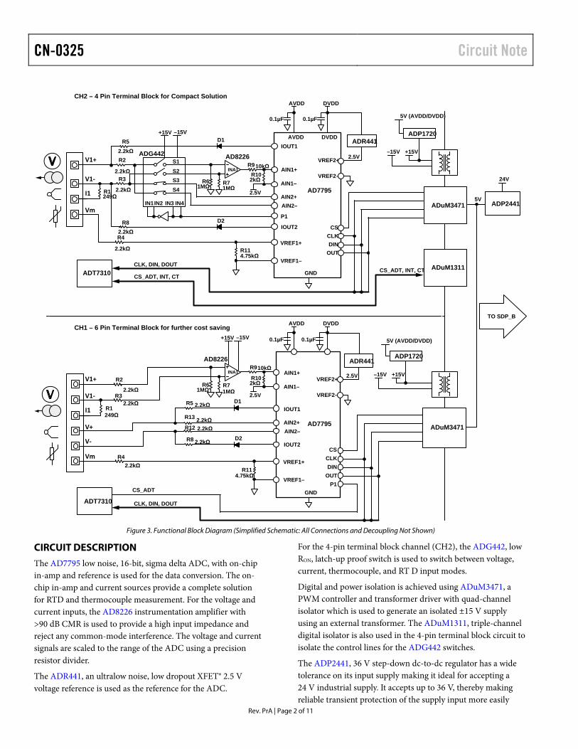
Figure 3. Functional Block Diagram (Simplified Schematic: All Connections and Decoupling Not Shown)
CIRCUIT DESCRIPTION The AD7795 low noise, 16-bit, sigma delta ADC, with on-chip in-amp and reference is used for the data conversion. The on-chip in-amp and current sources provide a complete solution for RTD and thermocouple measurement. For the voltage and current inputs, the AD8226 instrumentation amplifier with >90 dB CMR is used to provide a high input impedance and reject any common-mode interference. The voltage and current signals are scaled to the range of the ADC using a precision resistor divider.
The ADR441, an ultralow noise, low dropout XFET® 2.5 V voltage reference is used as the reference for the ADC.
For the 4-pin terminal block channel (CH2), the ADG442, low RON, latch-up proof switch is used to switch between voltage, current, thermocouple, and RT D input modes.
Digital and power isolation is achieved using ADuM3471, a PWM controller and transformer driver with quad-channel isolator which is used to generate an isolated ±15 V supply using an external transformer. The ADuM1311, triple-channel digital isolator is also used in the 4-pin terminal block circuit to isolate the control lines for the ADG442 switches.
The ADP2441, 36 V step-down dc-to-dc regulator has a wide tolerance on its input supply making it ideal for accepting a 24 V industrial supply. It accepts up to 36 V, thereby making reliable transient protection of the supply input more easily
AVDD DVDD
0.1µF 0.1µF
AD7795
ADT7310
5V (AVDD/DVDD)
AD7795
ADT7310
ADP2441
AIN1+
IOUT1
IOUT2
IOUT2
IOUT1
AIN1–
AIN1+
AIN1–
VREF1+
VREF1–
VREF1+
VREF1–
AVDD DVDD
GND
AIN2+AIN2–
AIN2+AIN2–
IN1IN2 IN3 IN4
P1
S1S2S3S4
D1
D2
ADG442
INA1
R1
R2
R2
R3
R5
R8
R11
R4
VREF2+
VREF2–
ADR441
2.5V
–15V+15V
–15V+15V
R1
R3R5
R8
2.5V
R6 R7
R9
R10
R4
2.5V
R13
R12
D1
D2
AD8226+15V–15V
+15V–15V
ADP1720
5V (AVDD/DVDD)
ADP1720
CSCLKDIN
OUT
VREF2+
VREF2–
CSCLKDIN
OUTP1
CS_ADT, INT, CTCS_ADT, INT, CT
CLK, DIN, DOUT
CLK, DIN, DOUT
CS_ADT
5V
24V
TO SDP_B
R11
AVDD DVDD
0.1µF 0.1µF
INA1
2.5V
R6 R7
R9
R10
AD8226
GND
ADR441
ADuM3471
ADuM1311
ADuM3471
V1+
V1-
I1
Vm
V1+
V1-
I1
V+
V-
Vm
1MΩ1MΩ
1MΩ1MΩ
249Ω
249Ω
2.2kΩ
2.2kΩ
2.2kΩ
4.75kΩ
2.2kΩ
4.75kΩ
2.2kΩ
2.2kΩ
2.2kΩ
2.2kΩ
2.2kΩ
2.2kΩ
2.2kΩ
2.2kΩ
10kΩ
2kΩ
2kΩ
10kΩ
CH2 – 4 Pin Terminal Block for Compact Solution
CH1 – 6 Pin Terminal Block for further cost saving
Circuit Note CN-0325
Rev. PrA | Page 3 of 11
achievable. It steps the input voltage down to 5 V to power the ADuM3471 as well as all other controller-side circuitry. The circuit also includes standard external protection on the 24 V supply terminals.
The ADP2441 also features a number of other safety and reliability functions, such as undervoltage lockout (UVLO), a precision enable, a power good pin, and overcurrent-limit protection. It also can achieve up to 90% efficiency in the 24 V input, 5 V output configuration.
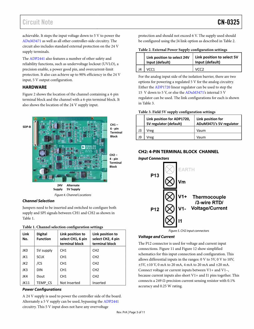
HARDWARE Figure 2 shows the location of the channel containing a 4-pin terminal block and the channel with a 6-pin terminal block. It also shows the location of the 24 V supply input.
Figure 4. Channel Locations
Channel Selection
Jumpers need to be inserted and switched to configure both supply and SPI signals between CH1 and CH2 as shown in Table 1.
Table 1. Channel selection configuration settings
Link No.
Digital Function
Link position to select CH1, 6 pin terminal block
Link position to select CH2, 4 pin terminal block
JK0 5V supply CH1 CH2
JK1 SCLK CH1 CH2
JK2 /CS CH1 CH2
JK3 DIN CH1 CH2
JK4 Dout CH1 CH2
JK11 TEMP_CS Not Inserted Inserted
Power Configurations
A 24 V supply is used to power the controller side of the board. Alternately a 5 V supply can be used, bypassing the ADP2441 circuitry. This 5 V input does not have any overvoltage
protection and should not exceed 6 V. The supply used should be configured using the J4 link option as described in Table 2.
Table 2. External Power Supply configuration settings
Link position to select 24V Input (default)
Link position to select 5V Input (default)
J4 VCC1 VCC2
For the analog input side of the isolation barrier, there are two options for powering a regulated 5 V for the analog circuitry. Either the ADP1720 linear regulator can be used to step the 15 V down to 5 V, or else the ADuM3471’s internal 5 V regulator can be used. The link configurations for each is shown in Table 3.
Table 3. Field 5V supply configuration settings
Link position for ADP1720, 5V regulator (default)
Link position for ADuM3471’s 5V regulator
J3 Vreg Vaum
J9 Vreg Vaum
CH2: 4-PIN TERMINAL BLOCK CHANNEL Input Connectors
Figure 5. CH2 input connectors
Voltage and Current
The P12 connector is used for voltage and current input connections. Figure 11 and Figure 12 show simplified schematics for this input connection and configuration. This allows differential inputs in the ranges: 0 V to 5V, 0 V to 10V, ±5V, ±10 V, 0 mA to 20 mA, 4 mA to 20 mA and ±20 mA. Connect voltage or current inputs between V1+ and V1–, because current inputs also short V1+ and I1 pins together. This connects a 249 Ω precision current sensing resistor with 0.1% accuracy and 0.25 W rating.
CH1 –6 - pin Terminal Block
CH2 –4 - pin Terminal Block
Alternate5V Supply
24VSupply
SDP-B
CN-0325 Circuit Note
Rev. PrA | Page 4 of 11
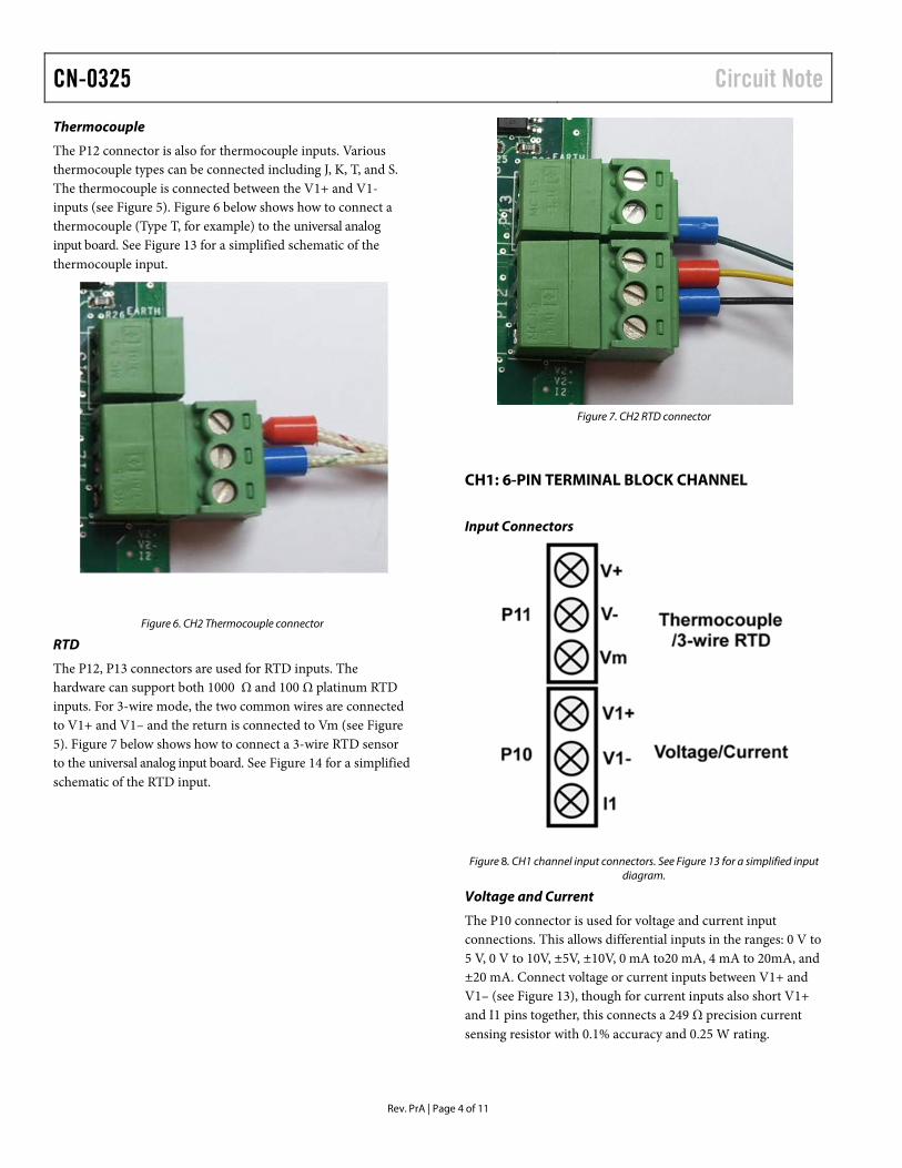
Thermocouple
The P12 connector is also for thermocouple inputs. Various thermocouple types can be connected including J, K, T, and S. The thermocouple is connected between the V1+ and V1- inputs (see Figure 5). Figure 6 below shows how to connect a thermocouple (Type T, for example) to the universal analog input board. See Figure 13 for a simplified schematic of the thermocouple input.
Figure 6. CH2 Thermocouple connector
RTD
The P12, P13 connectors are used for RTD inputs. The hardware can support both 1000 Ω and 100 Ω platinum RTD inputs. For 3-wire mode, the two common wires are connected to V1+ and V1– and the return is connected to Vm (see Figure 5). Figure 7 below shows how to connect a 3-wire RTD sensor to the universal analog input board. See Figure 14 for a simplified schematic of the RTD input.
Figure 7. CH2 RTD connector
CH1: 6-PIN TERMINAL BLOCK CHANNEL Input Connectors
Figure 8. CH1 channel input connectors. See Figure 13 for a simplified input diagram.
Voltage and Current
The P10 connector is used for voltage and current input connections. This allows differential inputs in the ranges: 0 V to 5 V, 0 V to 10V, ±5V, ±10V, 0 mA to20 mA, 4 mA to 20mA, and ±20 mA. Connect voltage or current inputs between V1+ and V1– (see Figure 13), though for current inputs also short V1+ and I1 pins together, this connects a 249 Ω precision current sensing resistor with 0.1% accuracy and 0.25 W rating.
Circuit Note CN-0325
Rev. PrA | Page 5 of 11
Thermocouple
The P11 connector is for thermocouple inputs. Various thermocouple types can be connected including J, K, T and S. The thermocouple is connected between the V+ and V- inputs (see Figure 8). Figure 9 below shows how to connect a thermocouple (Type T in this example) to the universal analog input board.
Figure 9. CH1 Thermocouple Connector
RTD
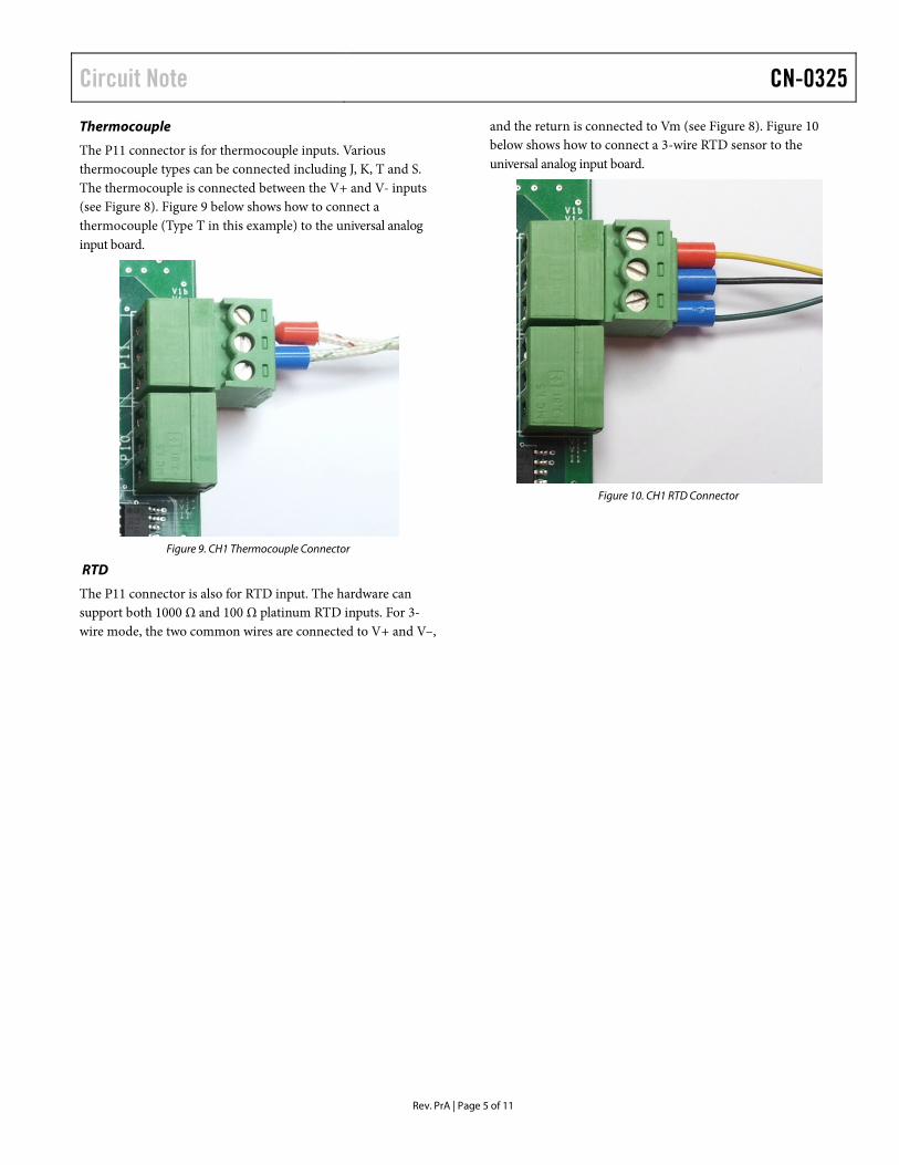
The P11 connector is also for RTD input. The hardware can support both 1000 Ω and 100 Ω platinum RTD inputs. For 3-wire mode, the two common wires are connected to V+ and V–,
and the return is connected to Vm (see Figure 8). Figure 10 below shows how to connect a 3-wire RTD sensor to the universal analog input board.
Figure 10. CH1 RTD Connector
Circuit Note CN-0325
Rev. PrA | Page 6 of 11
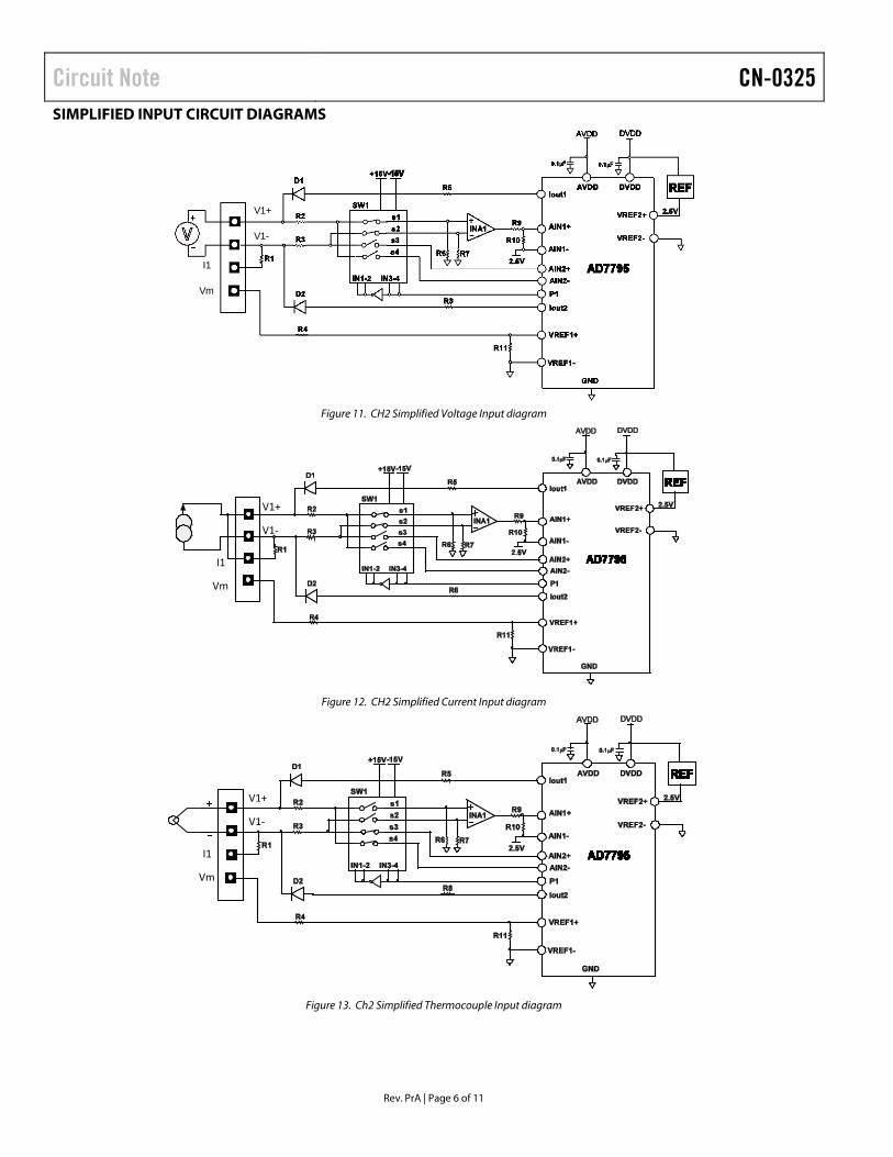
SIMPLIFIED INPUT CIRCUIT DIAGRAMS
Figure 11. CH2 Simplified Voltage Input diagram
Figure 12. CH2 Simplified Current Input diagram
Figure 13. Ch2 Simplified Thermocouple Input diagram
V1+
V1-
I1
Vm
V1+
V1-
I1
Vm
V1+
V1-
I1
Vm
Circuit Note CN-0325
Rev. PrA | Page 7 of 11
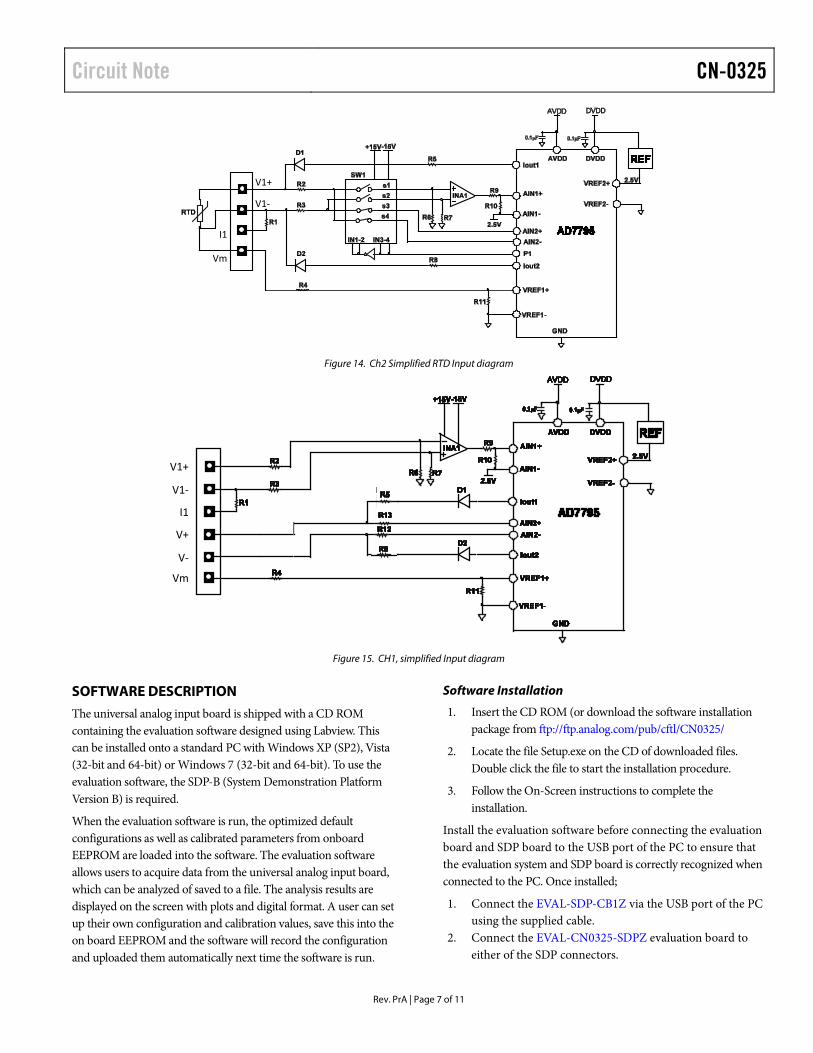
Figure 14. Ch2 Simplified RTD Input diagram
Figure 15. CH1, simplified Input diagram
SOFTWARE DESCRIPTION The universal analog input board is shipped with a CD ROM containing the evaluation software designed using Labview. This can be installed onto a standard PC with Windows XP (SP2), Vista (32-bit and 64-bit) or Windows 7 (32-bit and 64-bit). To use the evaluation software, the SDP-B (System Demonstration Platform Version B) is required.
When the evaluation software is run, the optimized default configurations as well as calibrated parameters from onboard EEPROM are loaded into the software. The evaluation software allows users to acquire data from the universal analog input board, which can be analyzed of saved to a file. The analysis results are displayed on the screen with plots and digital format. A user can set up their own configuration and calibration values, save this into the on board EEPROM and the software will record the configuration and uploaded them automatically next time the software is run.
Software Installation
1. Insert the CD ROM (or download the software installation package from ftp://ftp.analog.com/pub/cftl/CN0325/
2. Locate the file Setup.exe on the CD of downloaded files. Double click the file to start the installation procedure.
3. Follow the On-Screen instructions to complete the installation.
Install the evaluation software before connecting the evaluation board and SDP board to the USB port of the PC to ensure that the evaluation system and SDP board is correctly recognized when connected to the PC. Once installed;
1. Connect the EVAL-SDP-CB1Z via the USB port of the PC using the supplied cable.
2. Connect the EVAL-CN0325-SDPZ evaluation board to either of the SDP connectors.
V1+
V1-
I1
Vm
V1+
V1-
I1
V+
V-
Vm
CN-0325 Circuit Note
Rev. PrA | Page 8 of 11
3. Power up the EVAL-CN0325-SDPZ (Ensure jumpers are setup correctly as in the “Hardware” section)
4. Start the EVAL-CN0325-SDPZ software (“CN0325.exe”) and proceed through any dialog boxes that appear. This completes the installation.
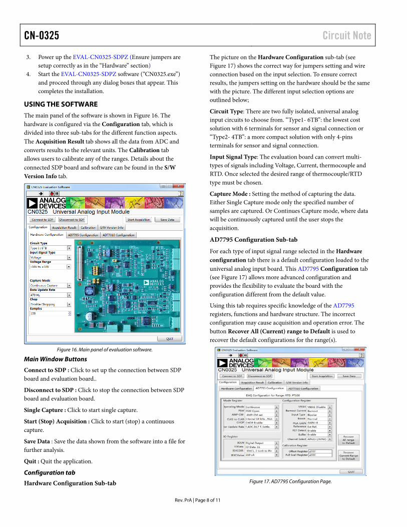
USING THE SOFTWARE The main panel of the software is shown in Figure 16. The hardware is configured via the Configuration tab, which is divided into three sub-tabs for the different function aspects. The Acquisition Result tab shows all the data from ADC and converts results to the relevant units. The Calibration tab allows users to calibrate any of the ranges. Details about the connected SDP board and software can be found in the S/W Version Info tab.
Figure 16. Main panel of evaluation software.
Main Window Buttons
Connect to SDP : Click to set up the connection between SDP board and evaluation board..
Disconnect to SDP : Click to stop the connection between SDP board and evaluation board.
Single Capture : Click to start single capture.
Start (Stop) Acquisition : Click to start (stop) a continuous capture.
Save Data : Save the data shown from the software into a file for further analysis.
Quit : Quit the application.
Configuration tab
Hardware Configuration Sub-tab
The picture on the Hardware Configuration sub-tab (see Figure 17) shows the correct way for jumpers setting and wire connection based on the input selection. To ensure correct results, the jumpers setting on the hardware should be the same with the picture. The different input selection options are outlined below;
Circuit Type: There are two fully isolated, universal analog input circuits to choose from. “Type1- 6TB”: the lowest cost solution with 6 terminals for sensor and signal connection or “Type2- 4TB”: a more compact solution with only 4-pins terminals for sensor and signal connection.
Input Signal Type: The evaluation board can convert multi-types of signals including Voltage, Current, thermocouple and RTD. Once selected the desired range of thermocouple/RTD type must be chosen.
Capture Mode : Setting the method of capturing the data. Either Single Capture mode only the specified number of samples are captured. Or Continues Capture mode, where data will be continuously captured until the user stops the acquisition.
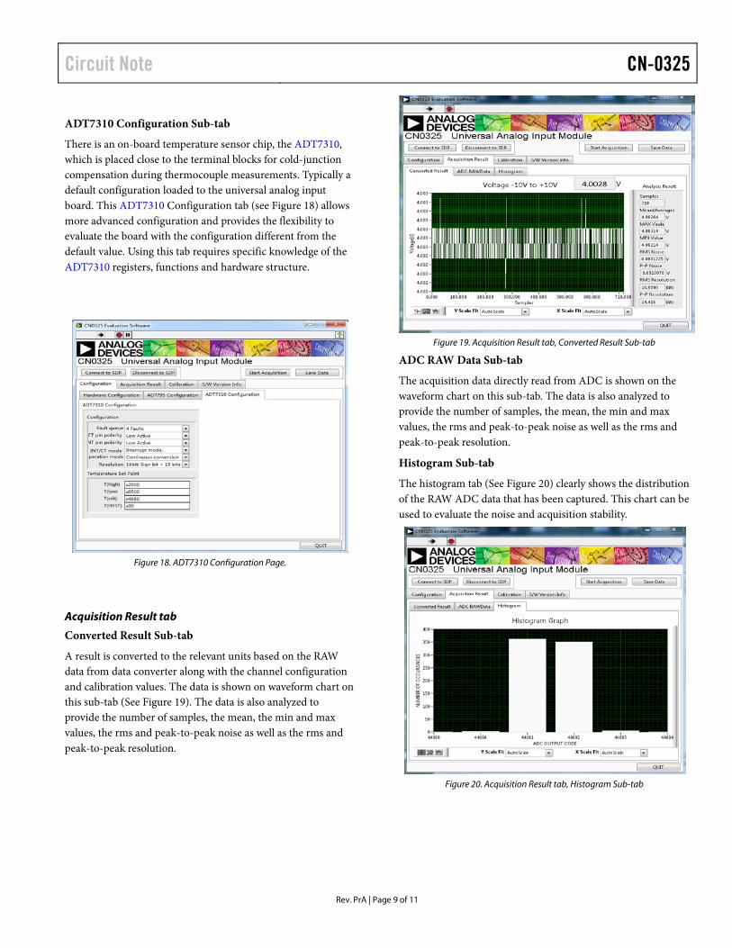
AD7795 Configuration Sub-tab
For each type of input signal range selected in the Hardware configuration tab there is a default configuration loaded to the universal analog input board. This AD7795 Configuration tab (see Figure 17) allows more advanced configuration and provides the flexibility to evaluate the board with the configuration different from the default value.
Using this tab requires specific knowledge of the AD7795 registers, functions and hardware structure. The incorrect configuration may cause acquisition and operation error. The button Recover All (Current) range to Default is used to recover the default configurations for the range(s).
Figure 17. AD7795 Configuration Page.
Circuit Note CN-0325
Rev. PrA | Page 9 of 11
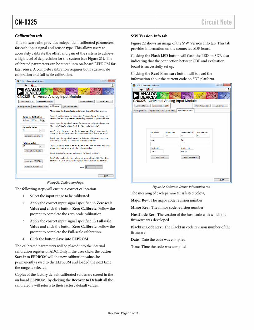
ADT7310 Configuration Sub-tab
There is an on-board temperature sensor chip, the ADT7310, which is placed close to the terminal blocks for cold-junction compensation during thermocouple measurements. Typically a default configuration loaded to the universal analog input board. This ADT7310 Configuration tab (see Figure 18) allows more advanced configuration and provides the flexibility to evaluate the board with the configuration different from the default value. Using this tab requires specific knowledge of the ADT7310 registers, functions and hardware structure.
Figure 18. ADT7310 Configuration Page.
Acquisition Result tab
Converted Result Sub-tab
A result is converted to the relevant units based on the RAW data from data converter along with the channel configuration and calibration values. The data is shown on waveform chart on this sub-tab (See Figure 19). The data is also analyzed to provide the number of samples, the mean, the min and max values, the rms and peak-to-peak noise as well as the rms and peak-to-peak resolution.
Figure 19. Acquisition Result tab, Converted Result Sub-tab
ADC RAW Data Sub-tab
The acquisition data directly read from ADC is shown on the waveform chart on this sub-tab. The data is also analyzed to provide the number of samples, the mean, the min and max values, the rms and peak-to-peak noise as well as the rms and peak-to-peak resolution.
Histogram Sub-tab
The histogram tab (See Figure 20) clearly shows the distribution of the RAW ADC data that has been captured. This chart can be used to evaluate the noise and acquisition stability.
Figure 20. Acquisition Result tab, Histogram Sub-tab
CN-0325 Circuit Note
Rev. PrA | Page 10 of 11
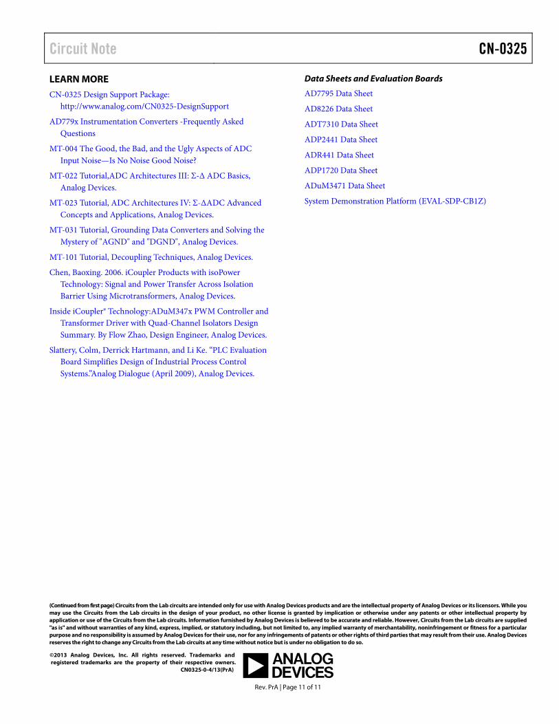
Calibration tab
This software also provides independent calibrated parameters for each input signal and sensor type. This allows users to accurately calibrate the offset and gain of the system to achieve a high level of dc precision for the system (see Figure 21). The calibrated parameters can be stored into on-board EEPROM for later reuse. A complete calibration requires both a zero-scale calibration and full-scale calibration.
Figure 21. Calibration Page.
The following steps will ensure a correct calibration.
1. Select the input range to be calibrated
2. Apply the correct input signal specified in Zeroscale Value and click the button Zero Calibrate. Follow the prompt to complete the zero-scale calibration.
3. Apply the correct input signal specified in Fullscale Value and click the button Zero Calibrate. Follow the prompt to complete the Full-scale calibration.
4. Click the button Save into EEPROM
The calibrated parameters will be placed into the internal calibration register of ADC. Only if the user clicks the button Save into EEPROM will the new calibration values be permanently saved to the EEPROM and loaded the next time the range is selected.
Copies of the factory default calibrated values are stored in the on board EEPROM. By clicking the Recover to Default all the calibrated v will return to their factory default values.
S\W Version Info tab
Figure 22 shows an image of the S\W Version Info tab. This tab provides information on the connected SDP board.
Clicking the Flash LED button will flash the LED on SDP, also indicating that the connection between SDP and evaluation board is successfully set up.
Clicking the Read Firmware button will to read the information about the current code on SDP platform.
Figure 22. Software Version Information tab
The meaning of each parameter is listed below;
Major Rev : The major code revision number
Minor Rev : The minor code revision number
HostCode Rev : The version of the host code with which the firmware was developed
BlackFinCode Rev : The BlackFin code revision number of the firmware
Date : Date the code was compiled
Time: Time the code was compiled
Circuit Note CN-0325
Rev. PrA | Page 11 of 11
LEARN MORE CN-0325 Design Support Package:
http://www.analog.com/CN0325-DesignSupport
AD779x Instrumentation Converters -Frequently Asked Questions
MT-004 The Good, the Bad, and the Ugly Aspects of ADC Input Noise—Is No Noise Good Noise?
MT-022 Tutorial,ADC Architectures III: Σ-Δ ADC Basics, Analog Devices.
MT-023 Tutorial, ADC Architectures IV: Σ-ΔADC Advanced Concepts and Applications, Analog Devices.
MT-031 Tutorial, Grounding Data Converters and Solving the Mystery of "AGND" and "DGND", Analog Devices.
MT-101 Tutorial, Decoupling Techniques, Analog Devices.
Chen, Baoxing. 2006. iCoupler Products with isoPower Technology: Signal and Power Transfer Across Isolation Barrier Using Microtransformers, Analog Devices.
Inside iCoupler® Technology:ADuM347x PWM Controller and Transformer Driver with Quad-Channel Isolators Design Summary. By Flow Zhao, Design Engineer, Analog Devices.
Slattery, Colm, Derrick Hartmann, and Li Ke. “PLC Evaluation Board Simplifies Design of Industrial Process Control Systems.”Analog Dialogue (April 2009), Analog Devices.
Data Sheets and Evaluation Boards
AD7795 Data Sheet
AD8226 Data Sheet
ADT7310 Data Sheet
ADP2441 Data Sheet
ADR441 Data Sheet
ADP1720 Data Sheet
ADuM3471 Data Sheet
System Demonstration Platform (EVAL-SDP-CB1Z)
(Continued from first page) Circuits from the Lab circuits are intended only for use with Analog Devices products and are the intellectual property of Analog Devices or its licensors. While you may use the Circuits from the Lab circuits in the design of your product, no other license is granted by implication or otherwise under any patents or other intellectual property by application or use of the Circuits from the Lab circuits. Information furnished by Analog Devices is believed to be accurate and reliable. However, Circuits from the Lab circuits are supplied "as is" and without warranties of any kind, express, implied, or statutory including, but not limited to, any implied warranty of merchantability, noninfringement or fitness for a particular purpose and no responsibility is assumed by Analog Devices for their use, nor for any infringements of patents or other rights of third parties that may result from their use. Analog Devices reserves the right to change any Circuits from the Lab circuits at any time without notice but is under no obligation to do so.
©2013 Analog Devices, Inc. All rights reserved. Trademarks and registered trademarks are the property of their respective owners. CN0325-0-4/13(PrA)


![LABORATÓRIO DE SISTEMAS MECATRÔNICOS E ROBÓTICA ] - LAB.pdf · Resistores - 1,0 Ω - 100k Ω 1,2 Ω - 120k Ω 1,5 Ω - 150k Ω 1,8 Ω- 180k Ω 2,2 Ω– 220k Ω 2,7 Ω– 270k](https://static.fdocument.org/doc/165x107/5c245c1a09d3f224508c4b48/laboratorio-de-sistemas-mecatronicos-e-robotica-labpdf-resistores-.jpg)