Chemical Vapour Deposition: CVD Reference: Jaeger …glennc/e495/e495l10j.pdf · Re l δ= l =...
31
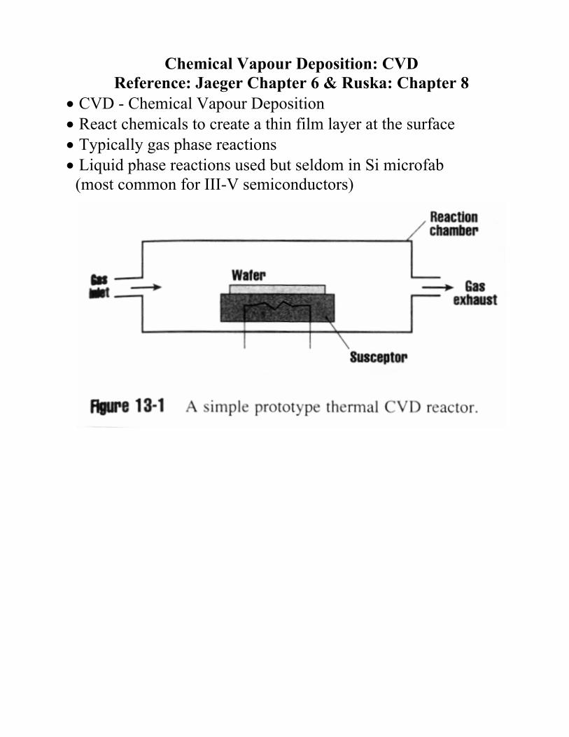
Chemical Vapour Deposition: CVD Reference: Jaeger Chapter 6 & Ruska: Chapter 8 • CVD - Chemical Vapour Deposition • React chemicals to create a thin film layer at the surface • Typically gas phase reactions • Liquid phase reactions used but seldom in Si microfab (most common for III-V semiconductors)
Transcript of Chemical Vapour Deposition: CVD Reference: Jaeger …glennc/e495/e495l10j.pdf · Re l δ= l =...
Chemical Vapour Deposition: CVD Reference: Jaeger Chapter 6 & Ruska: Chapter 8
• CVD - Chemical Vapour Deposition • React chemicals to create a thin film layer at the surface • Typically gas phase reactions • Liquid phase reactions used but seldom in Si microfab (most common for III-V semiconductors)
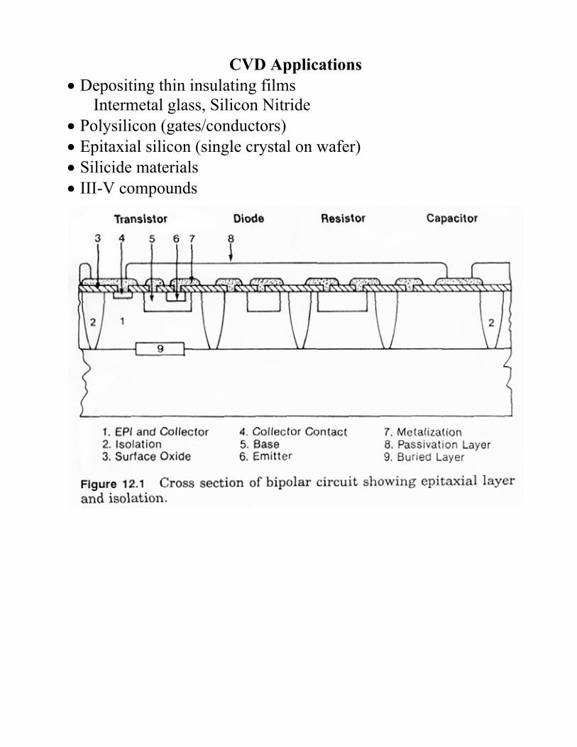
CVD Applications • Depositing thin insulating films Intermetal glass, Silicon Nitride • Polysilicon (gates/conductors) • Epitaxial silicon (single crystal on wafer) • Silicide materials • III-V compounds
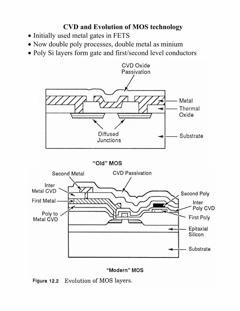
CVD and Evolution of MOS technology • Initially used metal gates in FETS • Now double poly processes, double metal as minium • Poly Si layers form gate and first/second level conductors
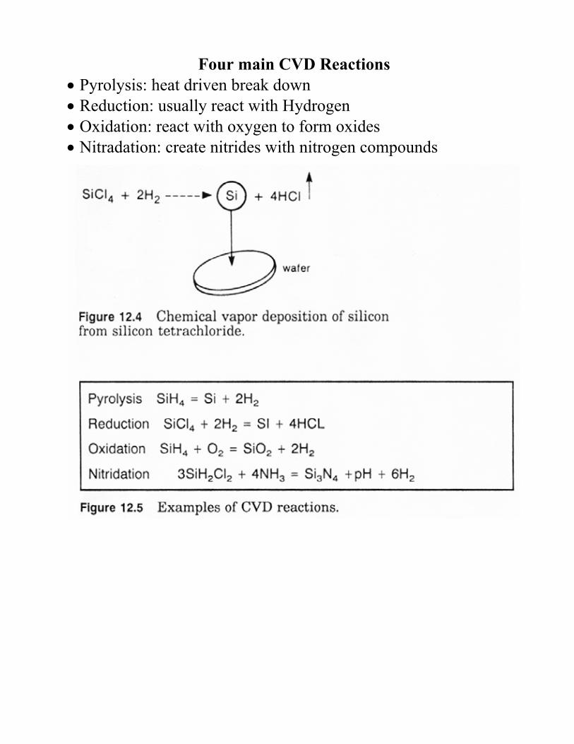
Four main CVD Reactions • Pyrolysis: heat driven break down • Reduction: usually react with Hydrogen • Oxidation: react with oxygen to form oxides • Nitradation: create nitrides with nitrogen compounds
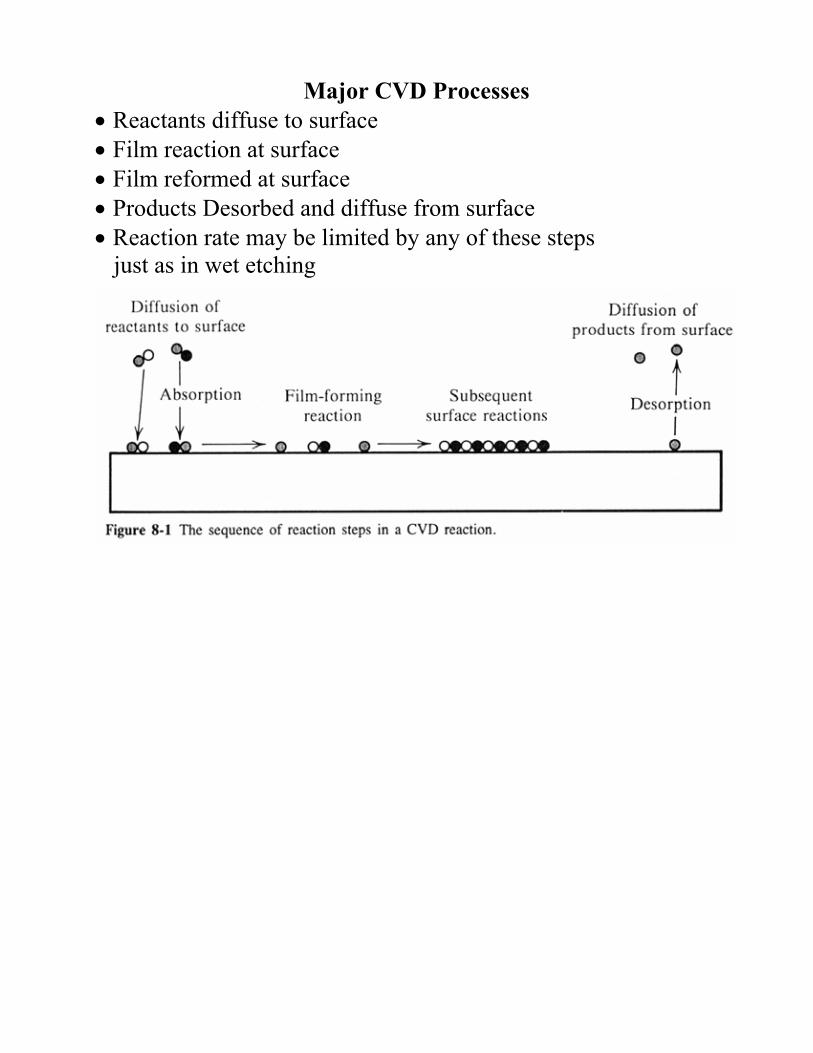
Major CVD Processes • Reactants diffuse to surface • Film reaction at surface • Film reformed at surface • Products Desorbed and diffuse from surface • Reaction rate may be limited by any of these steps just as in wet etching
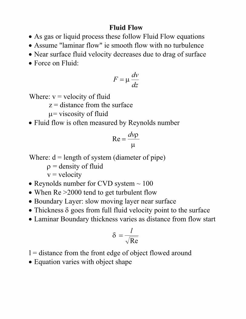
Fluid Flow • As gas or liquid process these follow Fluid Flow equations • Assume "laminar flow" ie smooth flow with no turbulence • Near surface fluid velocity decreases due to drag of surface • Force on Fluid:
dzdvF µ=
Where: v = velocity of fluid z = distance from the surface µ= viscosity of fluid • Fluid flow is often measured by Reynolds number
µρdv
=Re
Where: d = length of system (diameter of pipe) ρ = density of fluid v = velocity • Reynolds number for CVD system ~ 100 • When Re >2000 tend to get turbulent flow • Boundary Layer: slow moving layer near surface • Thickness δ goes from full fluid velocity point to the surface • Laminar Boundary thickness varies as distance from flow start
Rel
=δ
l = distance from the front edge of object flowed around • Equation varies with object shape
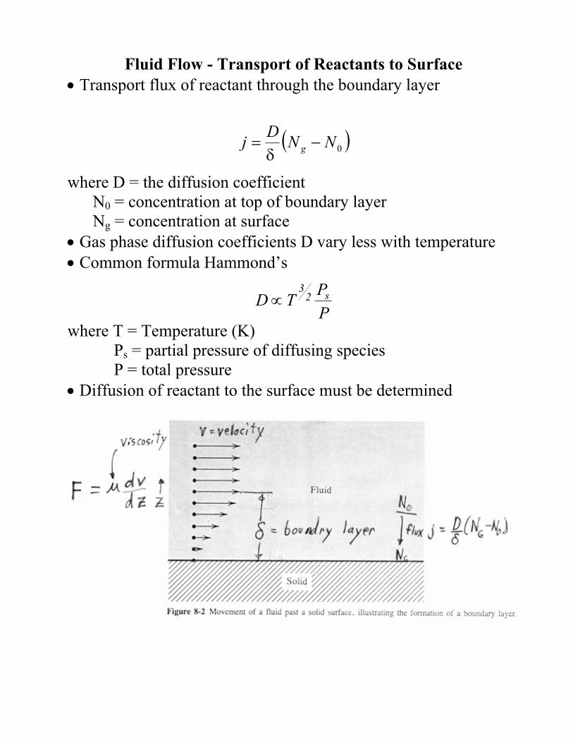
Fluid Flow - Transport of Reactants to Surface • Transport flux of reactant through the boundary layer
( )0NNDj g −=δ
where D = the diffusion coefficient N0 = concentration at top of boundary layer Ng = concentration at surface • Gas phase diffusion coefficients D vary less with temperature • Common formula Hammond’s
PPTD s2
3∝
where T = Temperature (K) Ps = partial pressure of diffusing species P = total pressure • Diffusion of reactant to the surface must be determined
Reaction at Substrate Surface • Flux at surface controlled by reaction
gsNkj =
where ks = surface reaction rate • Reaction rate flows an Arrhenius law
−
=KTEkk A
s exp'
where k' = reaction constant EA = Activation energy of the reaction KT = thermal energy • Thus the Reaction Flux at the surface
s
sg
kDkDN
jδ+
=
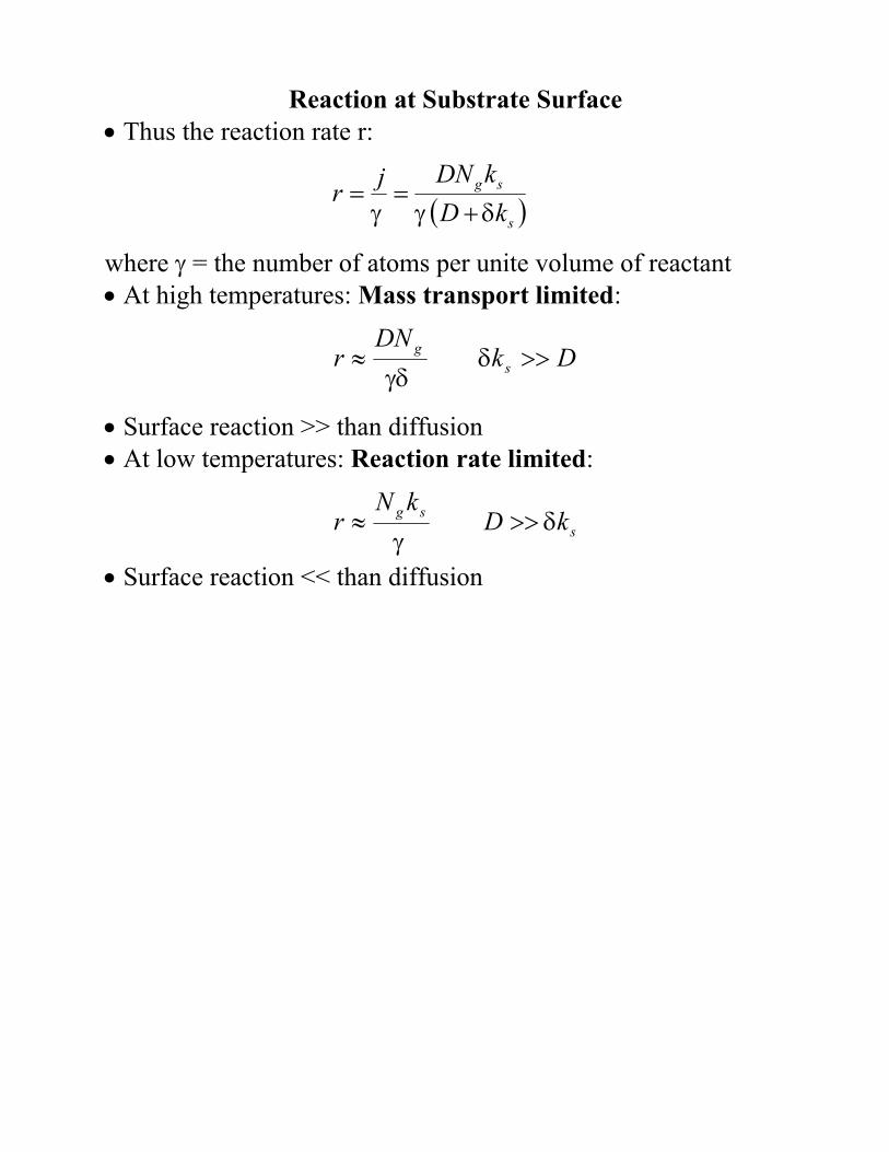
Reaction at Substrate Surface • Thus the reaction rate r:
( )ssg
kDkDNjrδγγ +
==
where γ = the number of atoms per unite volume of reactant • At high temperatures: Mass transport limited:
DkDN
r sg >>≈ δ
γδ
• Surface reaction >> than diffusion • At low temperatures: Reaction rate limited:
ssg kDkN
r δγ
>>≈
• Surface reaction << than diffusion
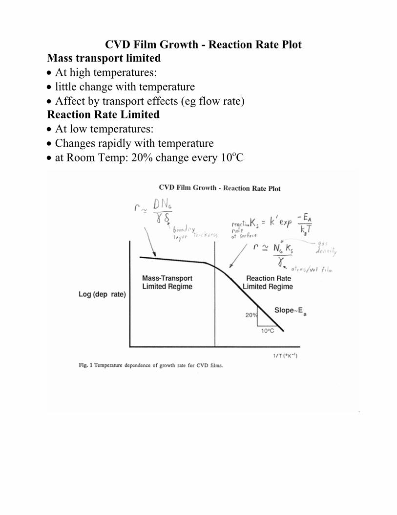
CVD Film Growth - Reaction Rate Plot Mass transport limited • At high temperatures: • little change with temperature • Affect by transport effects (eg flow rate) Reaction Rate Limited • At low temperatures: • Changes rapidly with temperature • at Room Temp: 20% change every 10oC
CVD Important film parameters • Stoichiometery: exact composition of film • Physical parameters: hardness, optical density • Electrical parameters: dielectric constant, breakdown voltage • Purity of film: lack of contamination • Thickness and uniformity • Conformality and step coverage • Pin hole (very small holes) and particle free • Adhesion (how well does film stick to surface)
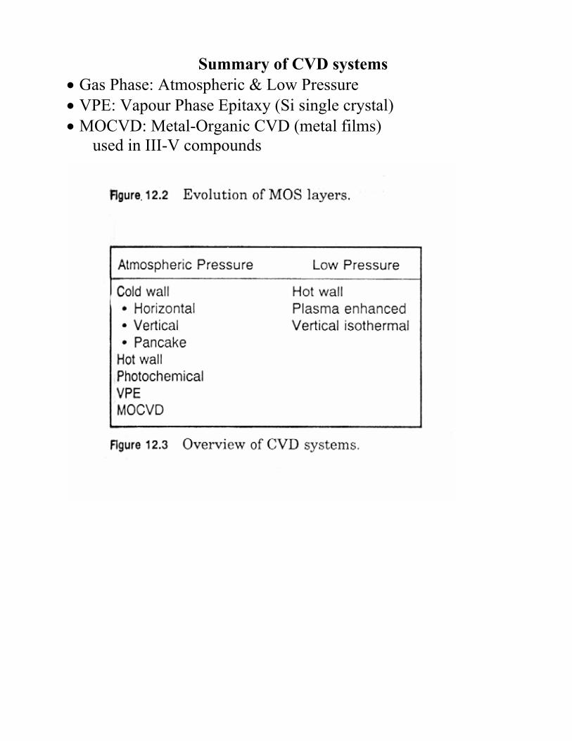
Summary of CVD systems • Gas Phase: Atmospheric & Low Pressure • VPE: Vapour Phase Epitaxy (Si single crystal) • MOCVD: Metal-Organic CVD (metal films) used in III-V compounds
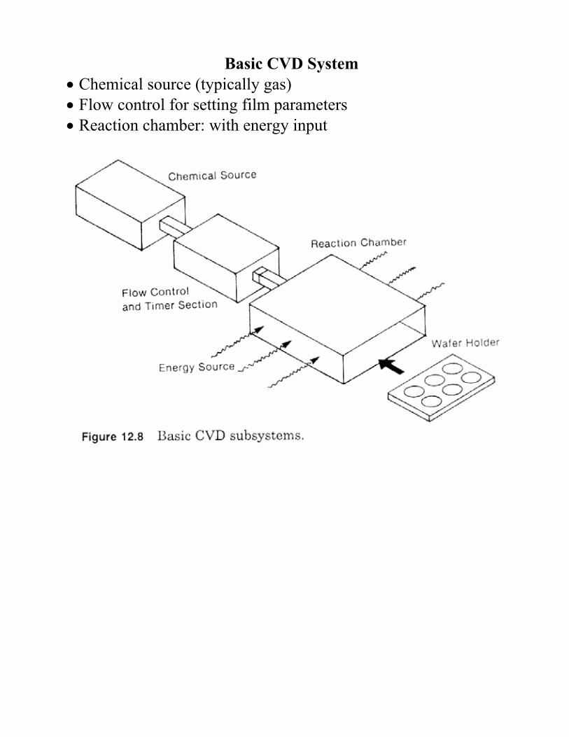
Basic CVD System • Chemical source (typically gas) • Flow control for setting film parameters • Reaction chamber: with energy input
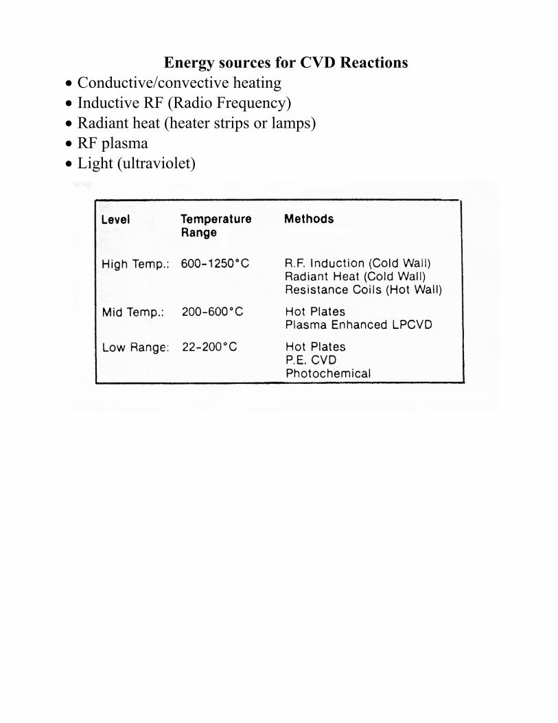
Energy sources for CVD Reactions • Conductive/convective heating • Inductive RF (Radio Frequency) • Radiant heat (heater strips or lamps) • RF plasma • Light (ultraviolet)
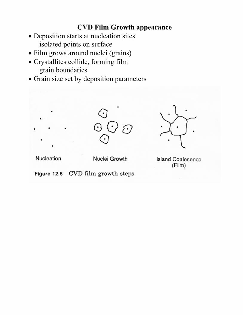
CVD Film Growth appearance • Deposition starts at nucleation sites isolated points on surface • Film grows around nuclei (grains) • Crystallites collide, forming film grain boundaries • Grain size set by deposition parameters
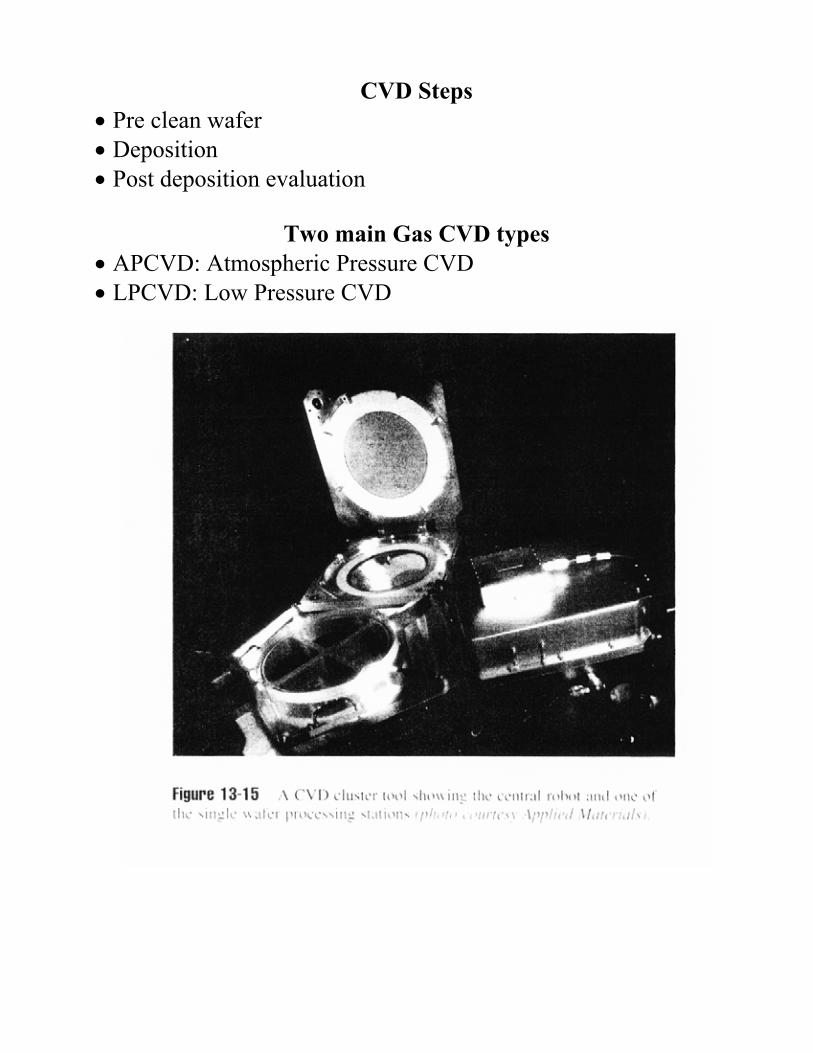
CVD Steps • Pre clean wafer • Deposition • Post deposition evaluation
Two main Gas CVD types • APCVD: Atmospheric Pressure CVD • LPCVD: Low Pressure CVD
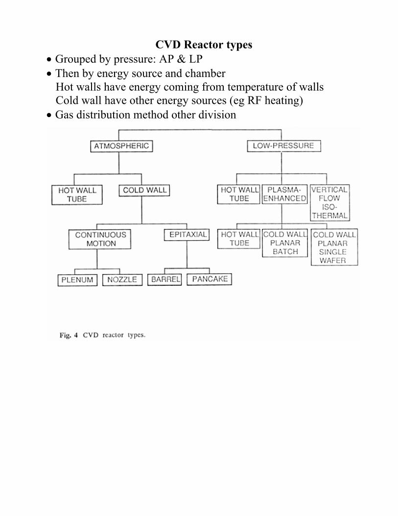
CVD Reactor types • Grouped by pressure: AP & LP • Then by energy source and chamber Hot walls have energy coming from temperature of walls Cold wall have other energy sources (eg RF heating) • Gas distribution method other division
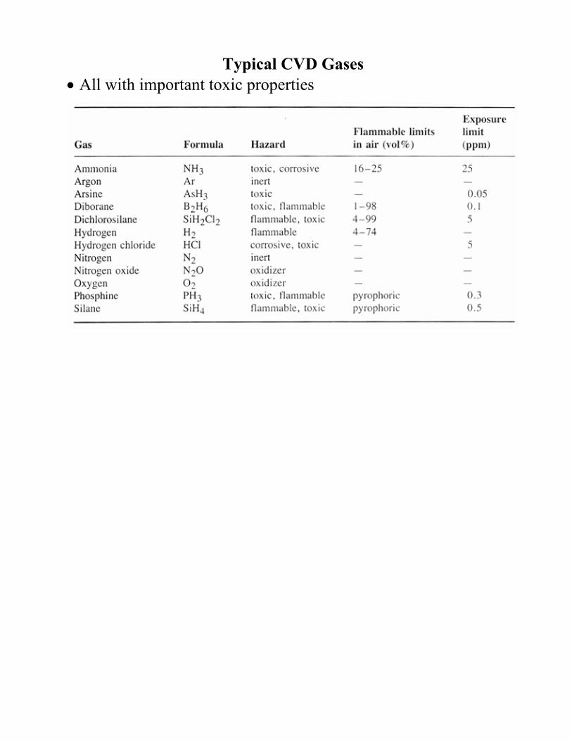
Typical CVD Gases • All with important toxic properties
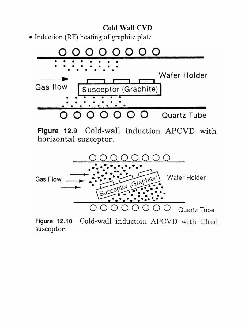
Cold Wall CVD • Induction (RF) heating of graphite plate
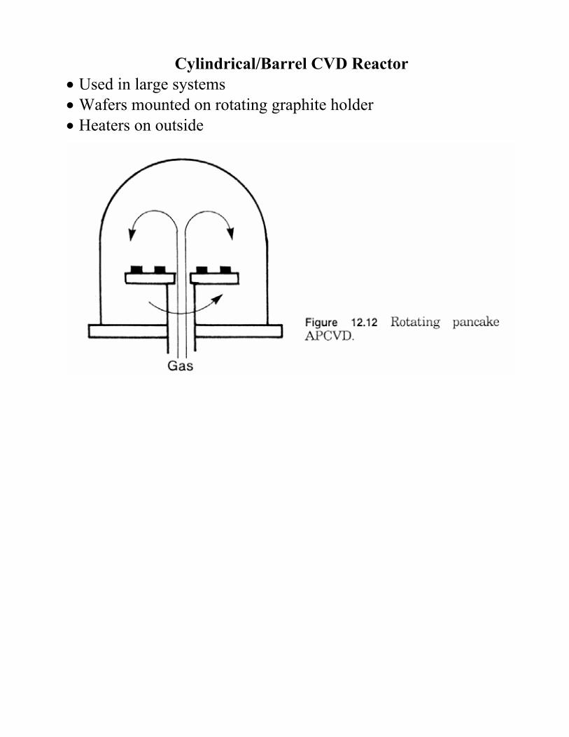
Cylindrical/Barrel CVD Reactor • Used in large systems • Wafers mounted on rotating graphite holder • Heaters on outside
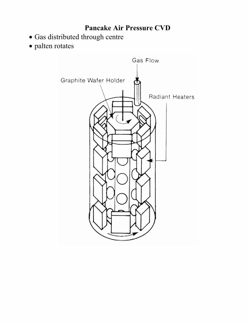
Pancake Air Pressure CVD • Gas distributed through centre • palten rotates
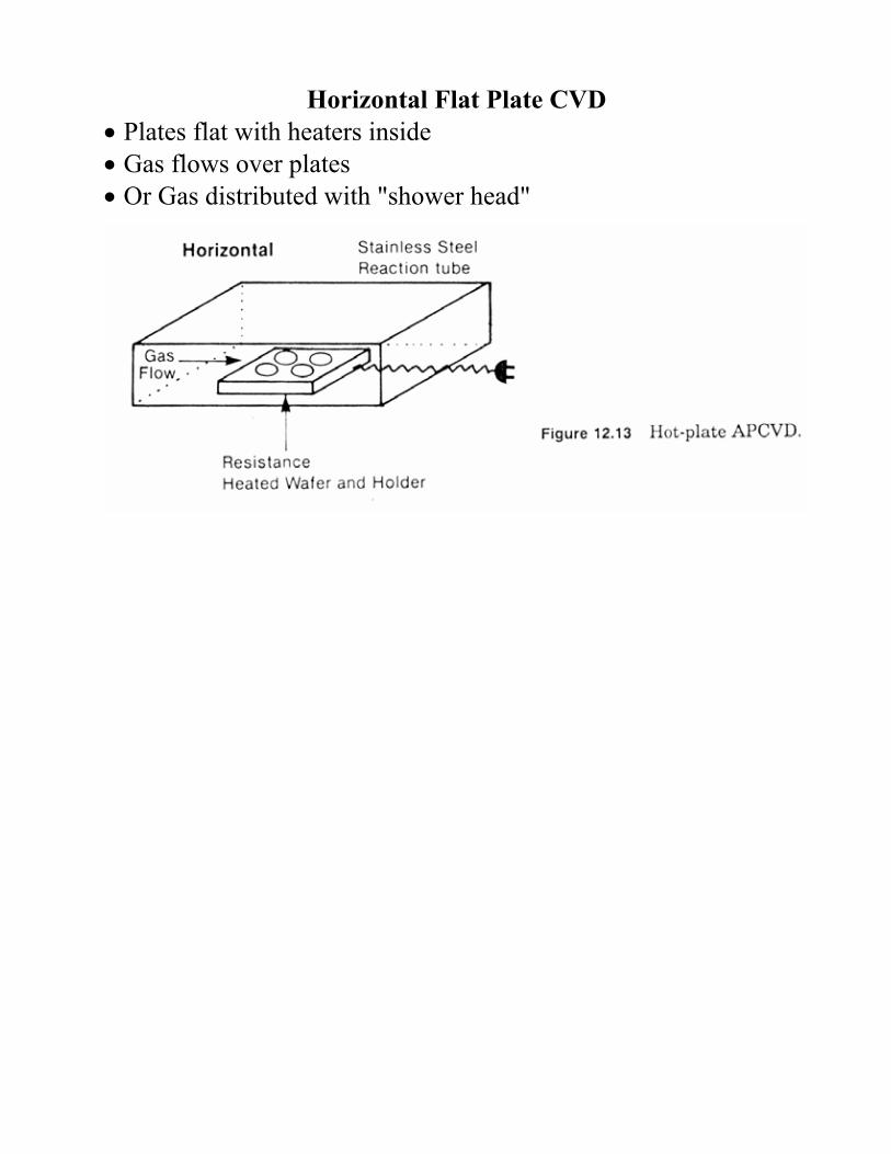
Horizontal Flat Plate CVD • Plates flat with heaters inside • Gas flows over plates • Or Gas distributed with "shower head"
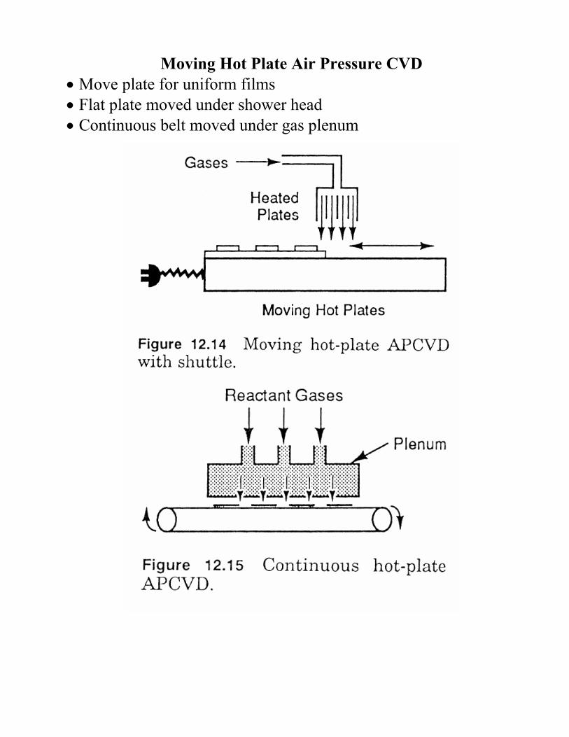
Moving Hot Plate Air Pressure CVD • Move plate for uniform films • Flat plate moved under shower head • Continuous belt moved under gas plenum
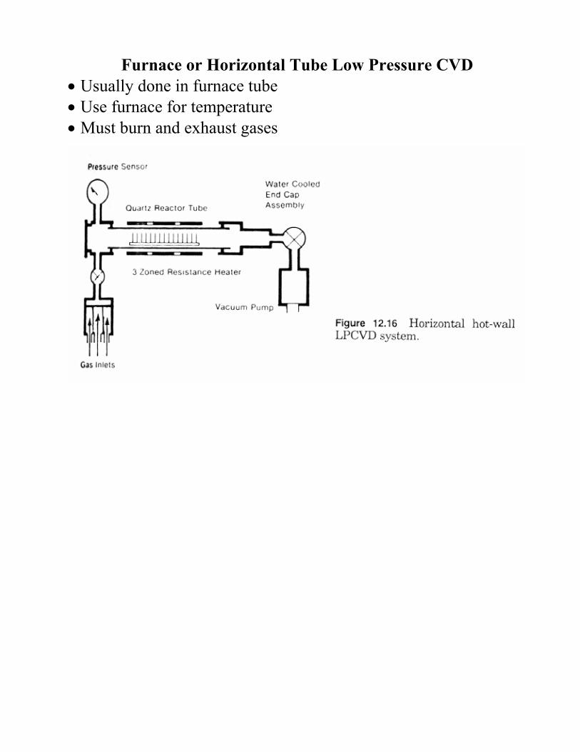
Furnace or Horizontal Tube Low Pressure CVD • Usually done in furnace tube • Use furnace for temperature • Must burn and exhaust gases
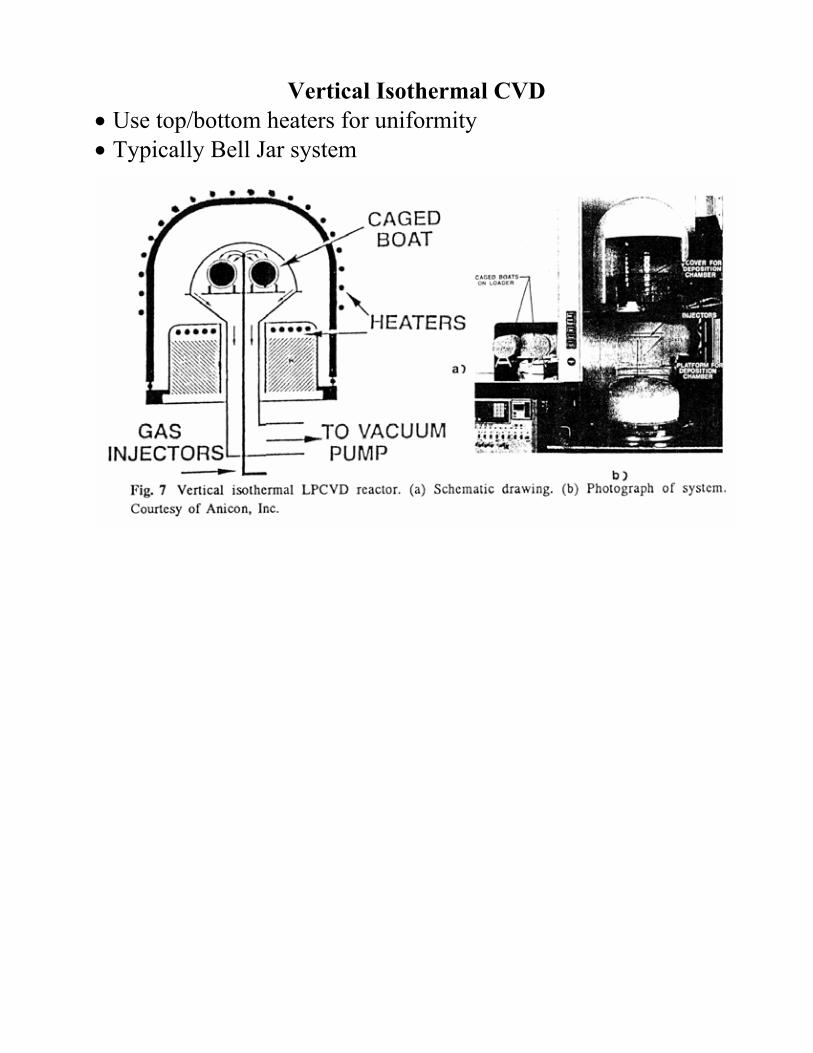
Vertical Isothermal CVD • Use top/bottom heaters for uniformity • Typically Bell Jar system
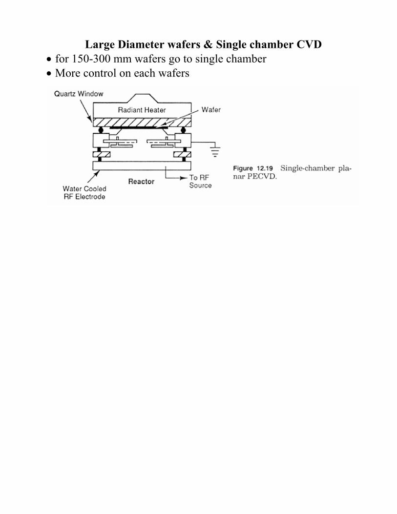
Large Diameter wafers & Single chamber CVD • for 150-300 mm wafers go to single chamber • More control on each wafers
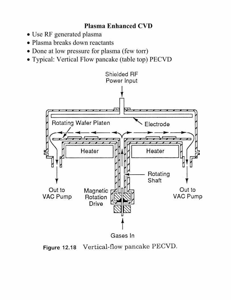
Plasma Enhanced CVD • Use RF generated plasma • Plasma breaks down reactants • Done at low pressure for plasma (few torr) • Typical: Vertical Flow pancake (table top) PECVD
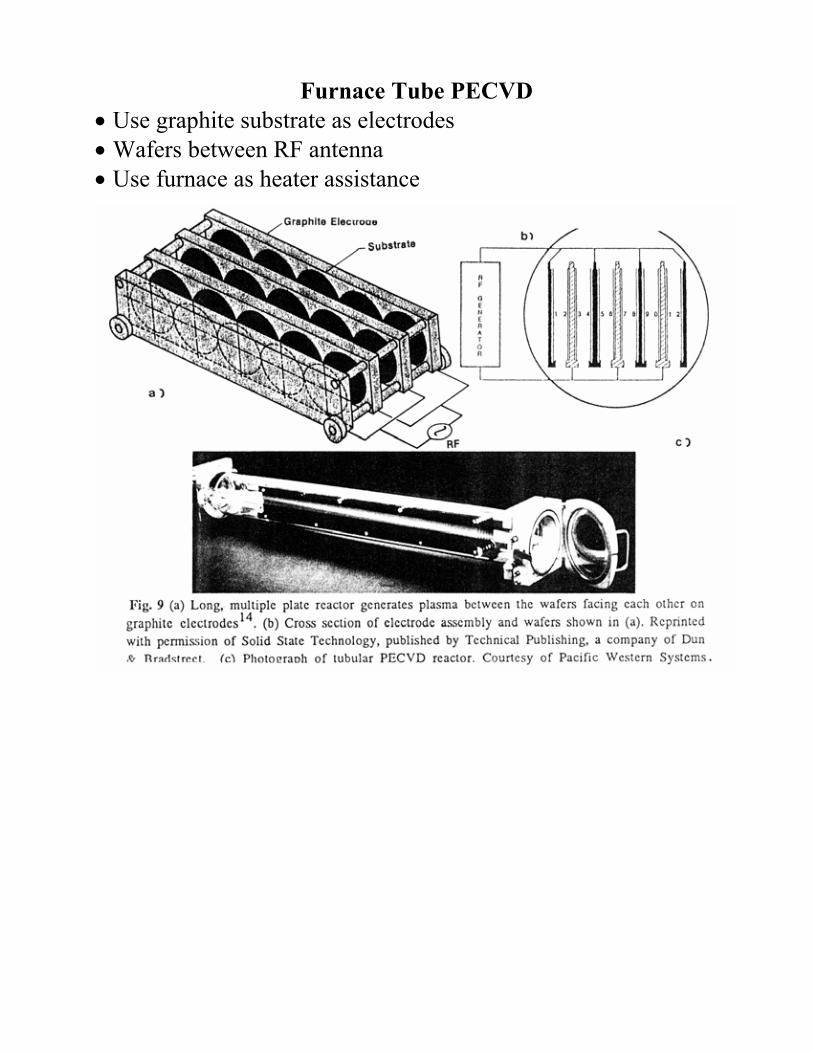
Furnace Tube PECVD • Use graphite substrate as electrodes • Wafers between RF antenna • Use furnace as heater assistance

Typical Furnace PECVD system • Temperature sets crystal size

Mass Flow Controller • Want to control mass of material • Feed back system needed: heats gas, measures temp. change • Get mass flowing form gas heat capacity
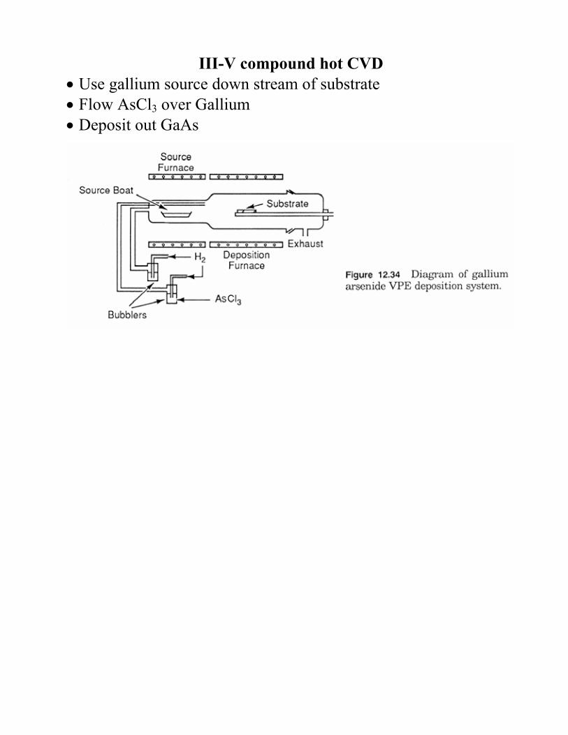
III-V compound hot CVD • Use gallium source down stream of substrate • Flow AsCl3 over Gallium • Deposit out GaAs