
Chapter 7: The Electronic Band Structure of Solidsjarrell/COURSES/SOLID_STATE/Chap7/chap7.pdf ·...
23
Chapter 7: The Electronic Band Structure of Solids Bloch & Slater March 2, 2017 Contents 1 Symmetry of ψ(r) 2 2 The nearly free Electron Approximation. 4 2.1 The Origin of Band Gaps ........................ 7 3 Tight Binding Approximation 10 4 Photo-Emission Spectroscopy 16 5 Anderson Localization 20 1
Transcript of Chapter 7: The Electronic Band Structure of Solidsjarrell/COURSES/SOLID_STATE/Chap7/chap7.pdf ·...
Chapter 7: The Electronic Band Structure of Solids
Bloch & Slater
March 2, 2017
Contents
1 Symmetry of ψ(r) 2
2 The nearly free Electron Approximation. 4
2.1 The Origin of Band Gaps . . . . . . . . . . . . . . . . . . . . . . . . 7
3 Tight Binding Approximation 10
4 Photo-Emission Spectroscopy 16
5 Anderson Localization 20
1
Free electrons -FLT Band Structure
E
Ef
D(E)
V(r)
Ef
Ef
metal
"heavy" metal
insulator
E
D(E)
V(r) = V0
Ef
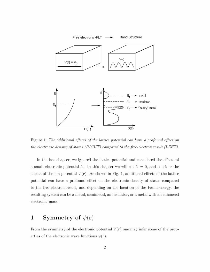
Figure 1: The additional effects of the lattice potential can have a profound effect on
the electronic density of states (RIGHT) compared to the free-electron result (LEFT).
In the last chapter, we ignored the lattice potential and considered the effects of
a small electronic potential U . In this chapter we will set U = 0, and consider the
effects of the ion potential V (r). As shown in Fig. 1, additional effects of the lattice
potential can have a profound effect on the electronic density of states compared
to the free-electron result, and depending on the location of the Fermi energy, the
resulting system can be a metal, semimetal, an insulator, or a metal with an enhanced
electronic mass.
1 Symmetry of ψ(r)
From the symmetry of the electronic potential V (r) one may infer some of the prop-
erties of the electronic wave functions ψ(r).
2
Due to the translational symmetry of the lattice V (r) is periodic
V (r) = V (r + rn), rn = n1a1 + n2a2 + n3a3 (1)
and may then be expanded in a Fourier expansion
V (r) =∑G
VGeiG·r, G = hg1 + kg2 + lg3 , (2)
which, since G · rn = 2πm (m ∈ Z) guarantees V (r) = V (r+ rn). Given this, and
letting ψ(r) =∑
kCkeik·r the Schroedinger equation becomes
Hψ(r) =
[− h̄2
2m∇2 + V (r)
]ψ = Eψ (3)
⇒∑k
h̄2k2
2mCke
ik·r +∑k′G
Ck′VGei(k′+G)·r = E
∑k
Ckeik·r, k′ → k−G (4)
X
X
X
X
X
X
First B.Z.
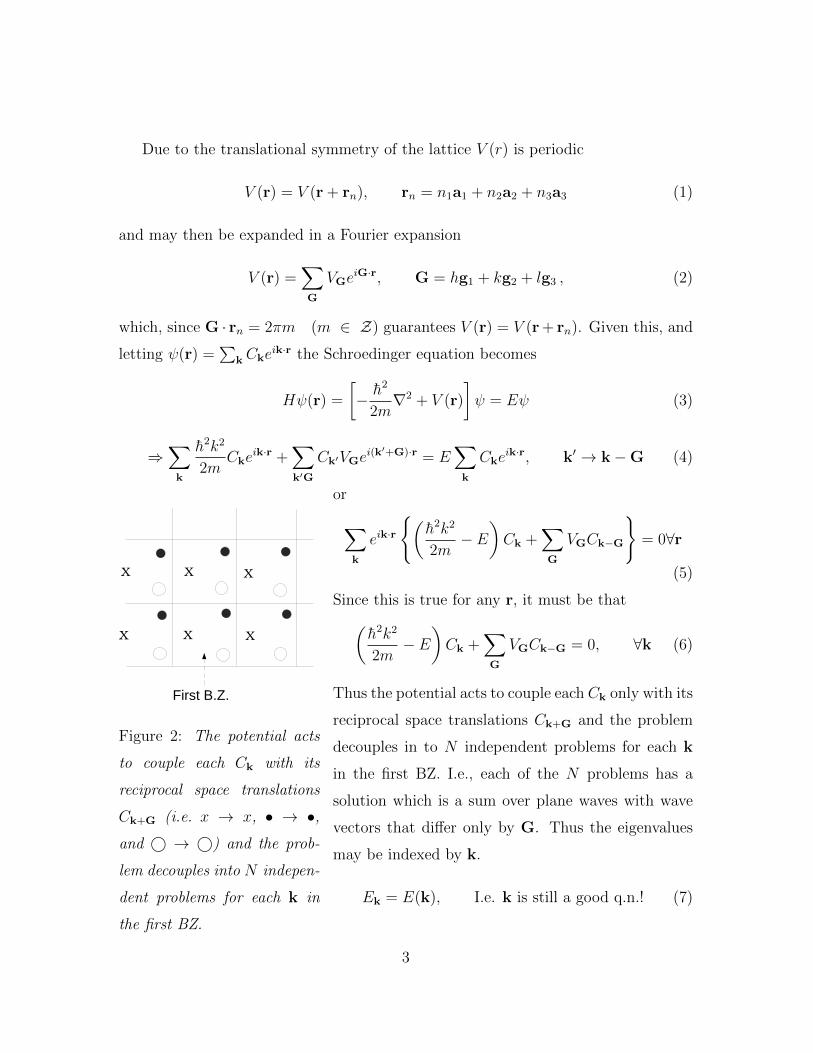
Figure 2: The potential acts
to couple each Ck with its
reciprocal space translations
Ck+G (i.e. x → x, • → •,and © → ©) and the prob-
lem decouples into N indepen-
dent problems for each k in
the first BZ.
or
∑k
eik·r
{(h̄2k2
2m− E
)Ck +
∑G
VGCk−G
}= 0∀r
(5)
Since this is true for any r, it must be that(h̄2k2
2m− E
)Ck +
∑G
VGCk−G = 0, ∀k (6)
Thus the potential acts to couple each Ck only with its
reciprocal space translations Ck+G and the problem
decouples in to N independent problems for each k
in the first BZ. I.e., each of the N problems has a
solution which is a sum over plane waves with wave
vectors that differ only by G. Thus the eigenvalues
may be indexed by k.
Ek = E(k), I.e. k is still a good q.n.! (7)
3
We may now sum over G to get ψk with the eigenvector sum restricted to recip-
rocal lattice sites k,k + G, . . .
ψk(r) =∑G
Ck−Gei(k−G)·r =
(∑G
Ck−Ge−iG·r
)eik·r (8)
ψk(r) = Uk(r)eik·r, where Uk(r) = Uk(r + rn) (9)
Note that if V (r) = 0, U(r) = 1√V
. This result is called Bloch’s Theorem; i.e., that
ψ may be resolved into a plane wave and a periodic function. Its consequences as
follows:
ψk+G(r) =∑G′
Ck+G−G′e−i(G′−k−G)·r =
(∑G′′
Ck−G′′e−iG′′·r
)eik·r
= ψk(r), where G′′ ≡ G′ −G (10)
I.e., ψk+G(r) = ψk(r) and as a result
Hψk = E(k)ψk ⇒ Hψk+G = E(k + G)ψk+G (11)
= Hψk = E(k + G)ψk+G (12)
Thus E(k+G) = E(k) : E(k) is periodic then since both ψk(r) and E(k) are periodic
in reciprocal space, one only needs knowledge of them in the first BZ to know them
everywhere.
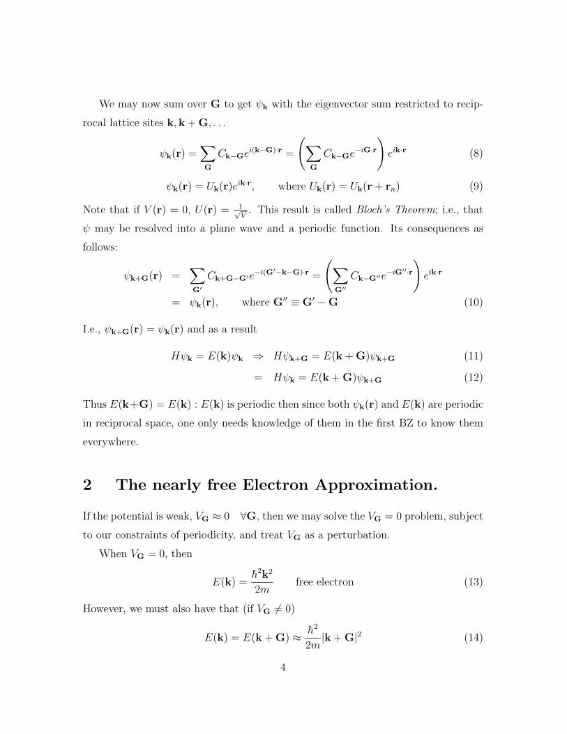
2 The nearly free Electron Approximation.
If the potential is weak, VG ≈ 0 ∀G, then we may solve the VG = 0 problem, subject
to our constraints of periodicity, and treat VG as a perturbation.
When VG = 0, then
E(k) =h̄2k2
2mfree electron (13)
However, we must also have that (if VG 6= 0)
E(k) = E(k + G) ≈ h̄2
2m|k + G|2 (14)
4
First BZ 2π/a
E
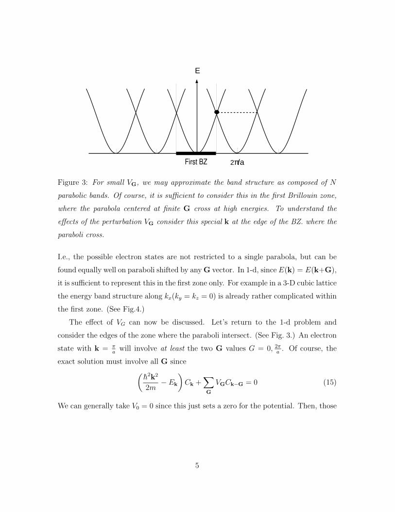
Figure 3: For small VG, we may approximate the band structure as composed of N
parabolic bands. Of course, it is sufficient to consider this in the first Brillouin zone,
where the parabola centered at finite G cross at high energies. To understand the
effects of the perturbation VG consider this special k at the edge of the BZ. where the
paraboli cross.
I.e., the possible electron states are not restricted to a single parabola, but can be
found equally well on paraboli shifted by any G vector. In 1-d, since E(k) = E(k+G),
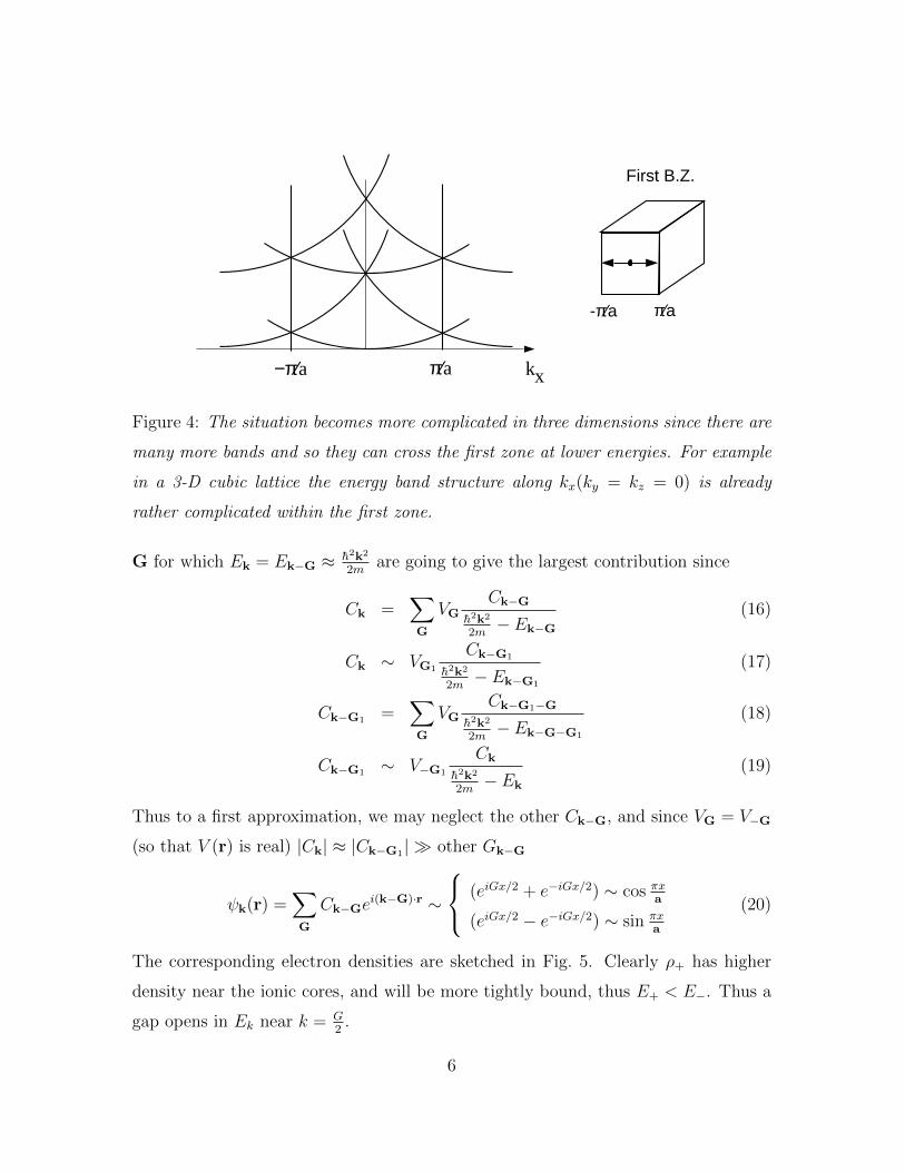
it is sufficient to represent this in the first zone only. For example in a 3-D cubic lattice
the energy band structure along kx(ky = kz = 0) is already rather complicated within
the first zone. (See Fig.4.)
The effect of VG can now be discussed. Let’s return to the 1-d problem and
consider the edges of the zone where the paraboli intersect. (See Fig. 3.) An electron
state with k = πa
will involve at least the two G values G = 0, 2πa
. Of course, the
exact solution must involve all G since(h̄2k2
2m− Ek
)Ck +
∑G
VGCk−G = 0 (15)
We can generally take V0 = 0 since this just sets a zero for the potential. Then, those
5
−π⁄a π⁄a kx
First B.Z.
π⁄a-π⁄a
Figure 4: The situation becomes more complicated in three dimensions since there are
many more bands and so they can cross the first zone at lower energies. For example
in a 3-D cubic lattice the energy band structure along kx(ky = kz = 0) is already
rather complicated within the first zone.
G for which Ek = Ek−G ≈ h̄2k2
2mare going to give the largest contribution since
Ck =∑G
VGCk−G
h̄2k2
2m− Ek−G
(16)
Ck ∼ VG1
Ck−G1
h̄2k2
2m− Ek−G1
(17)
Ck−G1 =∑G
VGCk−G1−G
h̄2k2
2m− Ek−G−G1
(18)
Ck−G1 ∼ V−G1
Ck
h̄2k2
2m− Ek
(19)
Thus to a first approximation, we may neglect the other Ck−G, and since VG = V−G
(so that V (r) is real) |Ck| ≈ |Ck−G1| � other Gk−G
ψk(r) =∑G
Ck−Gei(k−G)·r ∼
(eiGx/2 + e−iGx/2) ∼ cos πxa
(eiGx/2 − e−iGx/2) ∼ sin πxa
(20)
The corresponding electron densities are sketched in Fig. 5. Clearly ρ+ has higher
density near the ionic cores, and will be more tightly bound, thus E+ < E−. Thus a
gap opens in Ek near k = G2
.
6

V(x)
ρ (x)−
ρ (x)+E
k
Gap!
E
D(E)
Figure 5: ρ+ ∼ cos2(πx/a) has higher density near the ionic cores, and will be more
tightly bound, thus E+ < E−. Thus a gap opens in Ek near k = G2
.
2.1 The Origin of Band Gaps
Now let’s reexamine this gap at k = G1/2 in a quantitative manner. Start with the
eigen value equation shifted by G.
Ck−G
(Ek −
h̄2
2m|k−G|2
)=∑G′
VG′Ck−G−G′ =∑G′
VG′−GCk−G′ (21)
Ck−G =
∑G′ VG′−GCk−G′(
Ek − h̄2
2m|k−G|2
) (22)
To a first approximation (VG ' 0) let’s set E = h̄2k2
2m(a free-electron energy) and
ignore all but the largest Ck−G; i.e., those for which the denominator vanishes.
k2 = |k−G|2 , (23)
or in 1-d
k2 = (k− 2π
a)2 or k = −π
a(24)
This is just the Laue condition, which was shown to be equivalent to the Bragg
condition. I.e., the strongest perturbation to the free-electron picture occurs for
7
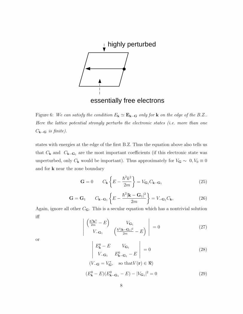
highly perturbed
essentially free electrons
Figure 6: We can satisfy the condition Ek ' Ek−G only for k on the edge of the B.Z..
Here the lattice potential strongly perturbs the electronic states (i.e. more than one
Ck−G is finite).
states with energies at the edge of the first B.Z. Thus the equation above also tells us
that Ck and Ck−G1 are the most important coefficients (if this electronic state was
unperturbed, only Ck would be important). Thus approximately for VG ∼ 0, V0 ≡ 0
and for k near the zone boundary
G = 0 Ck
{E − h̄2k2
2m
}= VG1Ck−G1 (25)
G = G1 Ck−G1
{E − h̄2|k−G1|2
2m
}= V−G1Ck, (26)
Again, ignore all other CG. This is a secular equation which has a nontrivial solution
iff ∣∣∣∣∣∣(h̄2k2
2m− E
)VG1
V−G1
(h̄2|k−G1|2
2m− E
)∣∣∣∣∣∣ = 0 (27)
or ∣∣∣∣∣∣ E0k − E VG1
V−G1 E0k−G1
− E
∣∣∣∣∣∣ = 0 (28)
(V−G = V ∗G, so thatV (r) ∈ <)
(E0k − E)(E0
k−G1− E)− |VG1|2 = 0 (29)
8
E0kE
0k−G1
− E(E0
k + E0k−G1
)+ E2 − |VG1|2 = 0 (30)
E± =1
2
(E0
k−G1+ E0
k
)±{
1
4
(E0
k−G − E0k
)2+ |VG1|2
} 12
(31)
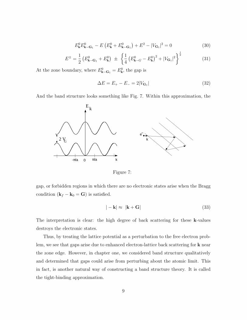
At the zone boundary, where E0k−G1
= E0k, the gap is
∆E = E+ − E− = 2|VG1| (32)
And the band structure looks something like Fig. 7. Within this approximation, the
-π/a π/a0 k
2 VG
Ek
ke−
Figure 7:
gap, or forbidden regions in which there are no electronic states arise when the Bragg
condition (kf − k0 = G) is satisfied.
| − k| ≈ |k + G| (33)
The interpretation is clear: the high degree of back scattering for these k-values
destroys the electronic states.
Thus, by treating the lattice potential as a perturbation to the free electron prob-
lem, we see that gaps arise due to enhanced electron-lattice back scattering for k near
the zone edge. However, in chapter one, we considered band structure qualitatively
and determined that gaps could arise from perturbing about the atomic limit. This
in fact, is another natural way of constructing a band structure theory. It is called
the tight-binding approximation.
9
Separation
StateEnergies
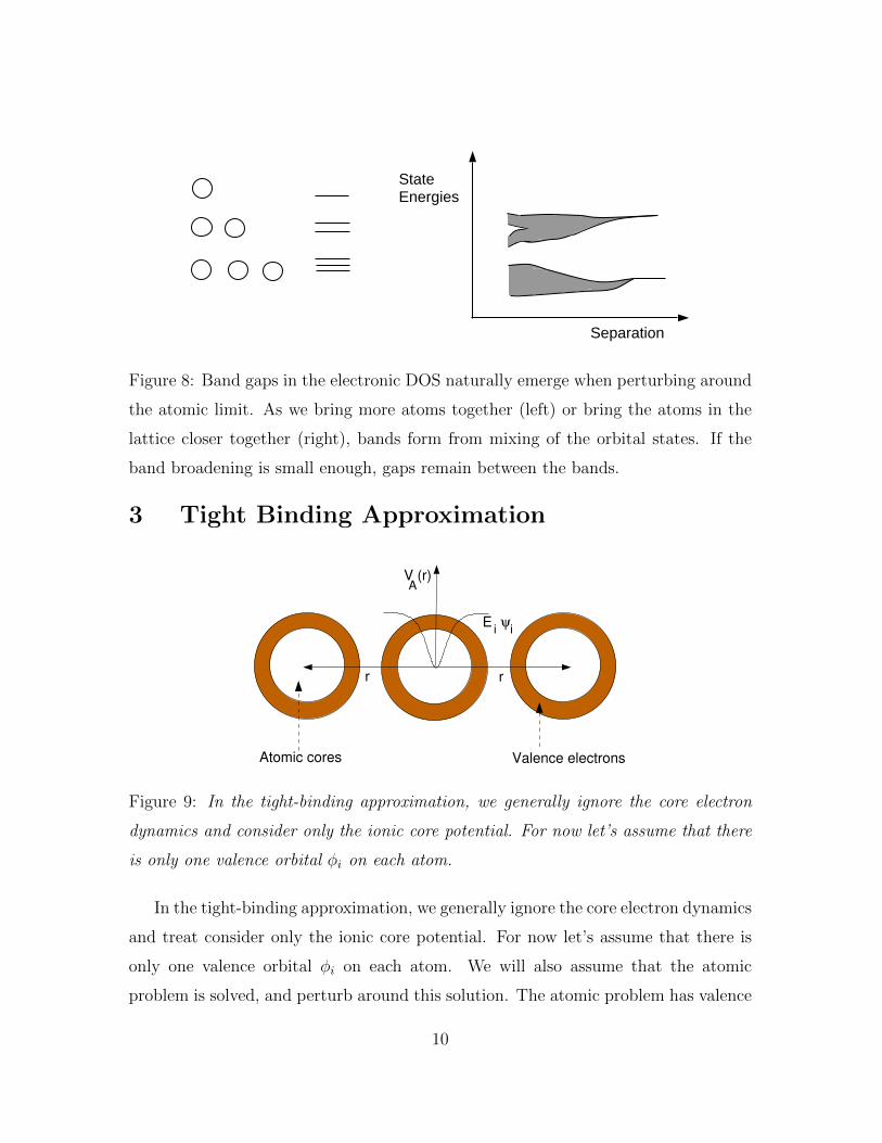
Figure 8: Band gaps in the electronic DOS naturally emerge when perturbing around
the atomic limit. As we bring more atoms together (left) or bring the atoms in the
lattice closer together (right), bands form from mixing of the orbital states. If the
band broadening is small enough, gaps remain between the bands.
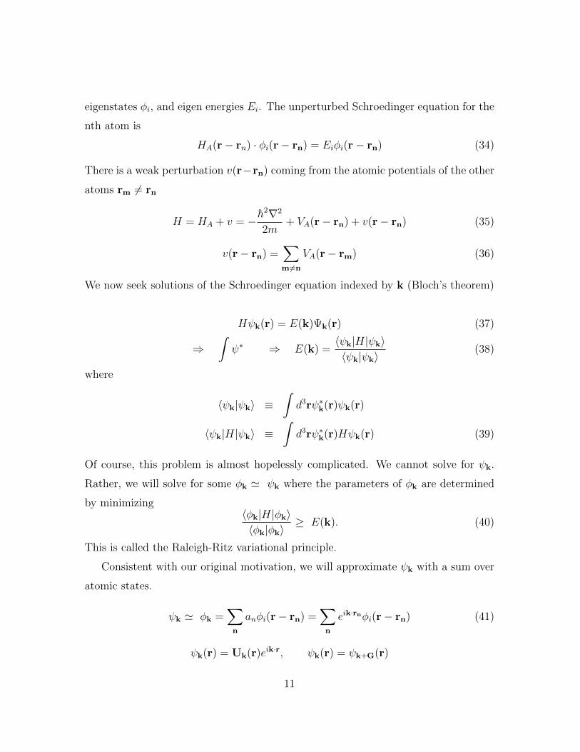
3 Tight Binding Approximation
r r
E ψi i
V (r)A
Valence electronsAtomic cores
Figure 9: In the tight-binding approximation, we generally ignore the core electron
dynamics and consider only the ionic core potential. For now let’s assume that there
is only one valence orbital φi on each atom.
In the tight-binding approximation, we generally ignore the core electron dynamics
and treat consider only the ionic core potential. For now let’s assume that there is
only one valence orbital φi on each atom. We will also assume that the atomic
problem is solved, and perturb around this solution. The atomic problem has valence
10
eigenstates φi, and eigen energies Ei. The unperturbed Schroedinger equation for the
nth atom is
HA(r− rn) · φi(r− rn) = Eiφi(r− rn) (34)
There is a weak perturbation v(r−rn) coming from the atomic potentials of the other
atoms rm 6= rn
H = HA + v = − h̄2∇2
2m+ VA(r− rn) + v(r− rn) (35)
v(r− rn) =∑m 6=n
VA(r− rm) (36)
We now seek solutions of the Schroedinger equation indexed by k (Bloch’s theorem)
Hψk(r) = E(k)Ψk(r) (37)
⇒∫ψ∗ ⇒ E(k) =
〈ψk|H|ψk〉〈ψk|ψk〉
(38)
where
〈ψk|ψk〉 ≡∫d3rψ∗k(r)ψk(r)
〈ψk|H|ψk〉 ≡∫d3rψ∗k(r)Hψk(r) (39)
Of course, this problem is almost hopelessly complicated. We cannot solve for ψk.
Rather, we will solve for some φk ' ψk where the parameters of φk are determined
by minimizing〈φk|H|φk〉〈φk|φk〉
≥ E(k). (40)
This is called the Raleigh-Ritz variational principle.
Consistent with our original motivation, we will approximate ψk with a sum over
atomic states.
ψk ' φk =∑n
anφi(r− rn) =∑n
eik·rnφi(r− rn) (41)
ψk(r) = Uk(r)eik·r, ψk(r) = ψk+G(r)
11
Where φk must be a Bloch state φk+G = φk which dictates our choice an = eik·rn .
Thus at this level of approximation we have no free parameters to vary to minimize
〈φk|H|φk〉 / 〈φk|φk〉 ≈ E(k).
Using φk as an approximate state the energy denominator 〈φk|φk〉, becomes
〈φk|φk〉 =∑n,m
eik·(rn−rm)
∫d3rφ∗i (r− rm)φi(r− rn) (42)
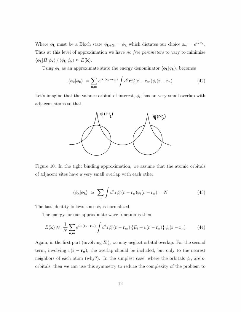
Let’s imagine that the valance orbital of interest, φi, has an very small overlap with
adjacent atoms so that
φ (r-r )i 1 φ (r-r )
i 2
Figure 10: In the tight binding approximation, we assume that the atomic orbitals
of adjacent sites have a very small overlap with each other.
〈φk|φk〉 '∑n
∫d3rφ∗i (r− rn)φi(r− rn) = N (43)
The last identity follows since φi is normalized.
The energy for our approximate wave function is then
E(k) ≈ 1
N
∑n,m
eik·(rn−rm)
∫d3rφ∗i (r− rm) {Ei + v(r− rn)}φi(r− rn) . (44)
Again, in the first part (involving Ei), we may neglect orbital overlap. For the second
term, involving v(r − rn), the overlap should be included, but only to the nearest
neighbors of each atom (why?). In the simplest case, where the orbitals φi, are s-
orbitals, then we can use this symmetry to reduce the complexity of the problem to
12
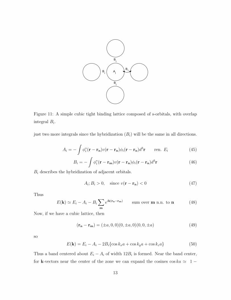
Ai
B iBi
Bi
Bi
Figure 11: A simple cubic tight binding lattice composed of s-orbitals, with overlap
integral Bi.
just two more integrals since the hybridization (Bi) will be the same in all directions.
Ai = −∫φ∗i (r− rn)v(r− rn)φi(r− rn)d3r ren. Ei (45)
Bi = −∫φ∗i (r− rm)v(r− rn)φi(r− rn)d3r (46)
Bi describes the hybridization of adjacent orbitals.
Ai;Bi > 0, since v(r− rn) < 0 (47)
Thus
E(k) ' Ei − Ai −Bi
∑m
eik(rn−rm) sum over m n.n. to n (48)
Now, if we have a cubic lattice, then
(rn − rm) = (±a, 0, 0)(0,±a, 0)(0, 0,±a) (49)
so
E(k) = Ei − Ai − 2Bi{cos kxa+ cos kya+ cos kza} (50)
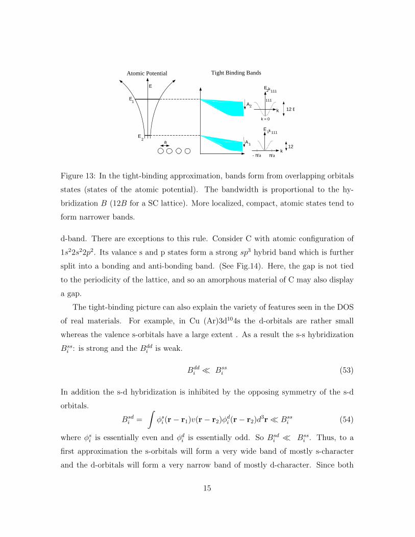
Thus a band centered about Ei −Ai of width 12Bi is formed. Near the band center,
for k-vectors near the center of the zone we can expand the cosines cos ka ' 1 −
13
12
(ka)2 + · · · and let k2 = k2x + k2
y + k2z , so that
E(k) ' Ei − Ai +Bia2k2 (51)
The electrons near the zone center act as if they were free with a renormalized mass.
h̄2k2
2m∗= Bia
2k2, i.e.1
m∗∝ curvature of band (52)
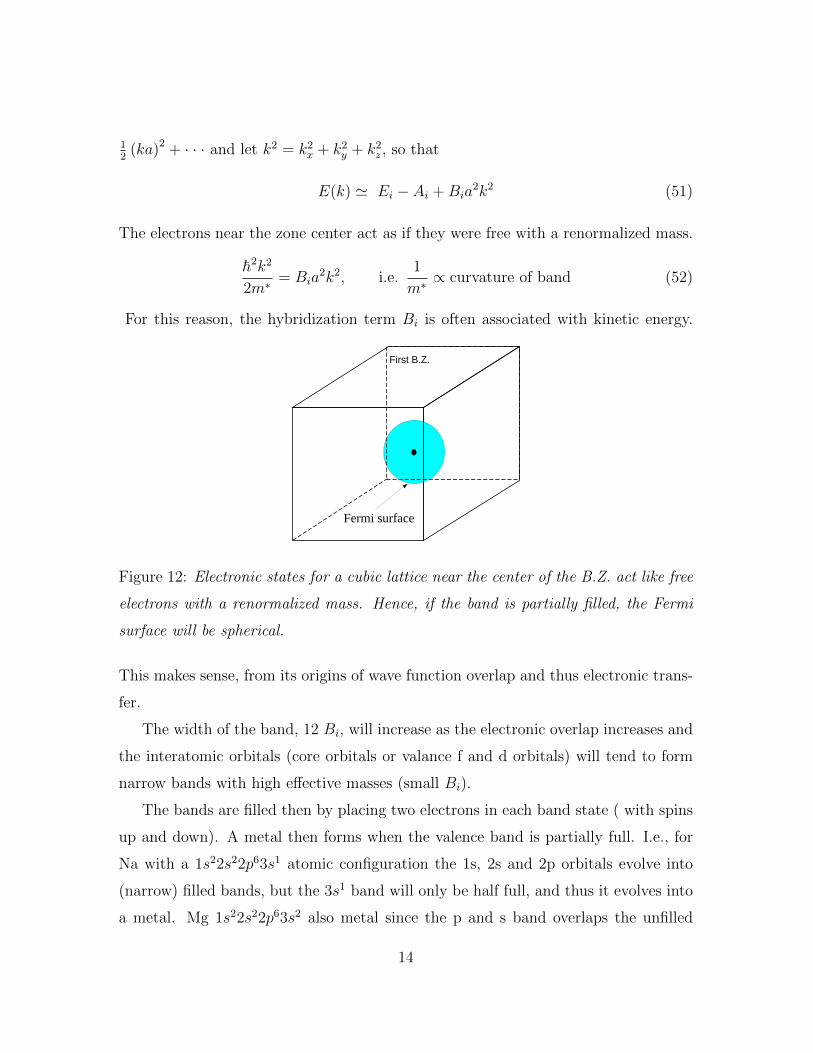
For this reason, the hybridization term Bi is often associated with kinetic energy.
First B.Z.
Fermi surface
Figure 12: Electronic states for a cubic lattice near the center of the B.Z. act like free
electrons with a renormalized mass. Hence, if the band is partially filled, the Fermi
surface will be spherical.
This makes sense, from its origins of wave function overlap and thus electronic trans-
fer.
The width of the band, 12 Bi, will increase as the electronic overlap increases and
the interatomic orbitals (core orbitals or valance f and d orbitals) will tend to form
narrow bands with high effective masses (small Bi).
The bands are filled then by placing two electrons in each band state ( with spins
up and down). A metal then forms when the valence band is partially full. I.e., for
Na with a 1s22s22p63s1 atomic configuration the 1s, 2s and 2p orbitals evolve into
(narrow) filled bands, but the 3s1 band will only be half full, and thus it evolves into
a metal. Mg 1s22s22p63s2 also metal since the p and s band overlaps the unfilled
14
a
E
E1
E1
E2
2E
1A
2A12 B
12 B
k = 0
- π/a π/a
k
k
k
k
111
111
111
Atomic Potential Tight Binding Bands
Figure 13: In the tight-binding approximation, bands form from overlapping orbitals
states (states of the atomic potential). The bandwidth is proportional to the hy-
bridization B (12B for a SC lattice). More localized, compact, atomic states tend to
form narrower bands.
d-band. There are exceptions to this rule. Consider C with atomic configuration of
1s22s22p2. Its valance s and p states form a strong sp3 hybrid band which is further
split into a bonding and anti-bonding band. (See Fig.14). Here, the gap is not tied
to the periodicity of the lattice, and so an amorphous material of C may also display
a gap.
The tight-binding picture can also explain the variety of features seen in the DOS
of real materials. For example, in Cu (Ar)3d104s the d-orbitals are rather small
whereas the valence s-orbitals have a large extent . As a result the s-s hybridization
Bssi : is strong and the Bdd
i is weak.
Bddi � Bss
i (53)
In addition the s-d hybridization is inhibited by the opposing symmetry of the s-d
orbitals.
Bsdi =
∫φsi (r− r1)v(r− r2)φdi (r− r2)d3r� Bss
i (54)
where φsi is essentially even and φdi is essentially odd. So Bsdi � Bss
i . Thus, to a
first approximation the s-orbitals will form a very wide band of mostly s-character
and the d-orbitals will form a very narrow band of mostly d-character. Since both
15
a
P
sp antibonding3
sp bonding3
S
a
E
r
Figure 14: C (diamond) with atomic configuration of 1s22s22p2. Its valance s and p
states form a strong sp3 hybrid band which is split into a bonding and anti-bonding
band.
+ +−
−
+1 2
+ +−
−
+ +−
−
d
s
D(E)
Figure 15: Schematic DOS of Cu 3d104s1. The narrow d-band feature is split due to
crystal fields.
the s and d bands are valance, they will overlap leading to a DOS with both d and s
features superimposed.
4 Photo-Emission Spectroscopy
The electronic density of electronic states (especially for occupied states), and to a less
extent band structure, are very important for illuminating the interesting physics of
materials. As we saw in Chap. 6, an enhanced DOS at the Fermi surface indicates an
enhanced electronic mass, and if D(EF ) = 0, we have an insulator (semiconductor).
16
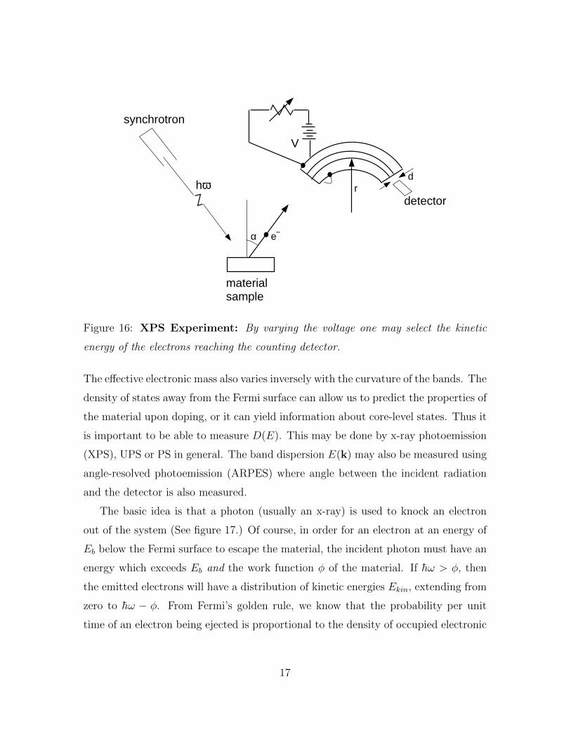
hωd
detector
synchrotron
r
materialsample
V
α e
Figure 16: XPS Experiment: By varying the voltage one may select the kinetic
energy of the electrons reaching the counting detector.
The effective electronic mass also varies inversely with the curvature of the bands. The
density of states away from the Fermi surface can allow us to predict the properties of
the material upon doping, or it can yield information about core-level states. Thus it
is important to be able to measure D(E). This may be done by x-ray photoemission
(XPS), UPS or PS in general. The band dispersion E(k) may also be measured using
angle-resolved photoemission (ARPES) where angle between the incident radiation
and the detector is also measured.
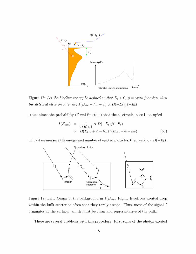
The basic idea is that a photon (usually an x-ray) is used to knock an electron
out of the system (See figure 17.) Of course, in order for an electron at an energy of
Eb below the Fermi surface to escape the material, the incident photon must have an
energy which exceeds Eb and the work function φ of the material. If h̄ω > φ, then
the emitted electrons will have a distribution of kinetic energies Ekin, extending from
zero to h̄ω − φ. From Fermi’s golden rule, we know that the probability per unit
time of an electron being ejected is proportional to the density of occupied electronic
17
Ehω - Eb
hω - E -φb
D(E)
Intensity(E)
Kinetic Energy of electrons hω - φ
X-ray
E b
Figure 17: Let the binding energy be defined so that Eb > 0, φ = work function, then
the detected electron intensity I(Ekin − h̄ω − φ) ∝ D(−Eb)f(−Eb)
states times the probability (Fermi function) that the electronic state is occupied
I(Ekin) =1
τ(Ekin)∝ D(−Eb)f(−Eb)
∝ D(Ekin + φ− h̄ω)f(Ekin + φ− h̄ω) (55)
Thus if we measure the energy and number of ejected particles, then we know D(−Eb).
phonon Coulombicinteration
Secondary electrons
e
e
Figure 18: Left: Origin of the background in I(Ekin. Right: Electrons excited deep
within the bulk scatter so often that they rarely escape. Thus, most of the signal I
originates at the surface, which must be clean and representative of the bulk.
There are several problems with this procedure. First some of the photon excited
18
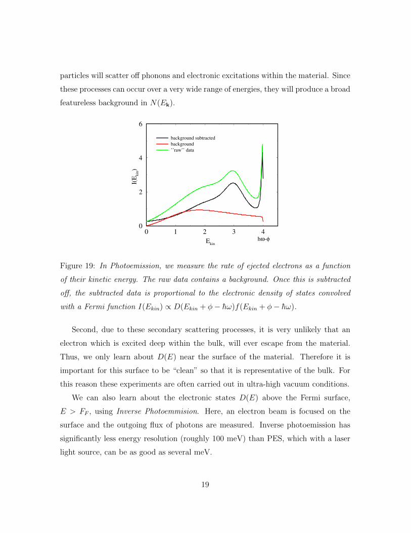
particles will scatter off phonons and electronic excitations within the material. Since
these processes can occur over a very wide range of energies, they will produce a broad
featureless background in N(Ek).
0 1 2 3 4
Ekin
0
2
4
6
I(E
kin)
background subtracted
background
’’raw’’ data
hω-φ
Figure 19: In Photoemission, we measure the rate of ejected electrons as a function
of their kinetic energy. The raw data contains a background. Once this is subtracted
off, the subtracted data is proportional to the electronic density of states convolved
with a Fermi function I(Ekin) ∝ D(Ekin + φ− h̄ω)f(Ekin + φ− h̄ω).
Second, due to these secondary scattering processes, it is very unlikely that an
electron which is excited deep within the bulk, will ever escape from the material.
Thus, we only learn about D(E) near the surface of the material. Therefore it is
important for this surface to be “clean” so that it is representative of the bulk. For
this reason these experiments are often carried out in ultra-high vacuum conditions.
We can also learn about the electronic states D(E) above the Fermi surface,
E > FF , using Inverse Photoemmision. Here, an electron beam is focused on the
surface and the outgoing flux of photons are measured. Inverse photoemission has
significantly less energy resolution (roughly 100 meV) than PES, which with a laser
light source, can be as good as several meV.
19
5 Anderson Localization
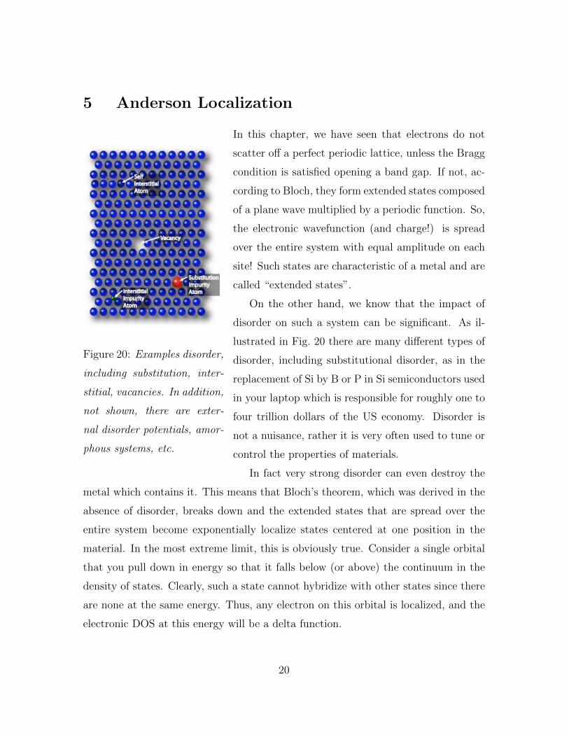
Figure 20: Examples disorder,
including substitution, inter-
stitial, vacancies. In addition,
not shown, there are exter-
nal disorder potentials, amor-
phous systems, etc.
In this chapter, we have seen that electrons do not
scatter off a perfect periodic lattice, unless the Bragg
condition is satisfied opening a band gap. If not, ac-
cording to Bloch, they form extended states composed
of a plane wave multiplied by a periodic function. So,
the electronic wavefunction (and charge!) is spread
over the entire system with equal amplitude on each
site! Such states are characteristic of a metal and are
called “extended states”.
On the other hand, we know that the impact of
disorder on such a system can be significant. As il-
lustrated in Fig. 20 there are many different types of
disorder, including substitutional disorder, as in the
replacement of Si by B or P in Si semiconductors used
in your laptop which is responsible for roughly one to
four trillion dollars of the US economy. Disorder is
not a nuisance, rather it is very often used to tune or
control the properties of materials.
In fact very strong disorder can even destroy the
metal which contains it. This means that Bloch’s theorem, which was derived in the
absence of disorder, breaks down and the extended states that are spread over the
entire system become exponentially localize states centered at one position in the
material. In the most extreme limit, this is obviously true. Consider a single orbital
that you pull down in energy so that it falls below (or above) the continuum in the
density of states. Clearly, such a state cannot hybridize with other states since there
are none at the same energy. Thus, any electron on this orbital is localized, and the
electronic DOS at this energy will be a delta function.
20
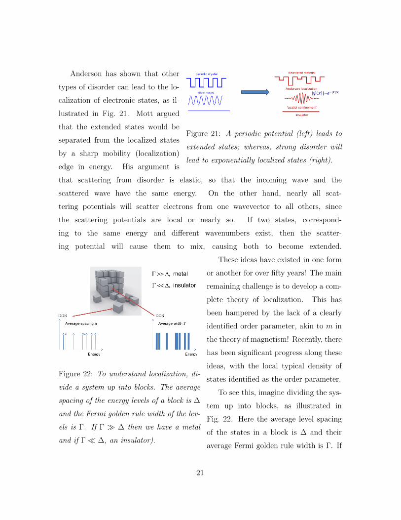
Figure 21: A periodic potential (left) leads to
extended states; whereas, strong disorder will
lead to exponentially localized states (right).
Anderson has shown that other
types of disorder can lead to the lo-
calization of electronic states, as il-
lustrated in Fig. 21. Mott argued
that the extended states would be
separated from the localized states
by a sharp mobility (localization)
edge in energy. His argument is
that scattering from disorder is elastic, so that the incoming wave and the
scattered wave have the same energy. On the other hand, nearly all scat-
tering potentials will scatter electrons from one wavevector to all others, since
the scattering potentials are local or nearly so. If two states, correspond-
ing to the same energy and different wavenumbers exist, then the scatter-
ing potential will cause them to mix, causing both to become extended.
Figure 22: To understand localization, di-
vide a system up into blocks. The average
spacing of the energy levels of a block is ∆
and the Fermi golden rule width of the lev-
els is Γ. If Γ � ∆ then we have a metal
and if Γ� ∆, an insulator).
These ideas have existed in one form
or another for over fifty years! The main
remaining challenge is to develop a com-
plete theory of localization. This has
been hampered by the lack of a clearly
identified order parameter, akin to m in
the theory of magnetism! Recently, there
has been significant progress along these
ideas, with the local typical density of
states identified as the order parameter.
To see this, imagine dividing the sys-
tem up into blocks, as illustrated in
Fig. 22. Here the average level spacing
of the states in a block is ∆ and their
average Fermi golden rule width is Γ. If
21
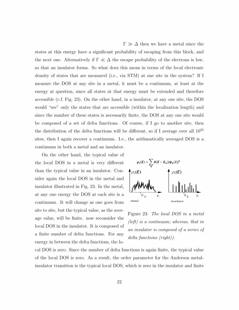
Γ � ∆ then we have a metal since the
states at this energy have a significant probability of escaping from this block, and
the next one. Alternatively if Γ � ∆ the escape probability of the electrons is low,
so that an insulator forms. So what does this mean in terms of the local electronic
density of states that are measured (i.e., via STM) at one site in the system? If I
measure the DOS at any site in a metal, it must be a continuum, at least at the
energy at question, since all states at that energy must be extended and therefore
accessible (c.f. Fig. 23). On the other hand, in a insulator, at any one site, the DOS
would “see” only the states that are accessible (within the localization length) and
since the number of these states is necessarily finite, the DOS at any one site would
be composed of a set of delta functions. Of course, if I go to another site, then
the distribution of the delta functions will be different, so if I average over all 1023
sites, then I again recover a continuum. I.e., the arithmatically averaged DOS is a
continuum in both a metal and an insulator.
Figure 23: The local DOS in a metal
(left) is a continuum; whereas, that in
an insulator is composed of a series of
delta functions (right)).
On the other hand, the typical value of
the local DOS in a metal is very different
than the typical value in an insulator. Con-
sider again the local DOS in the metal and
insulator illustrated in Fig. 23. In the metal,
at any one energy the DOS at each site is a
continuum. It will change as one goes from
site to site, but the typical value, as the aver-
age value, will be finite. now reconsider the
local DOS in the insulator. It is composed of
a finite number of delta functions. For any
energy in between the delta functions, the lo-
cal DOS is zero. Since the number of delta functions is again finite, the typical value
of the local DOS is zero. As a result, the order parameter for the Anderson metal-
insulator transition is the typical local DOS, which is zero in the insulator and finite
22
in the metal.
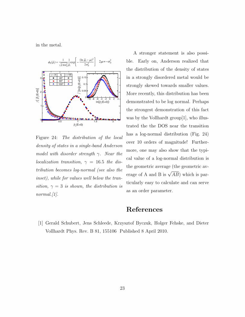
Figure 24: The distribution of the local
density of states in a single-band Anderson
model with disorder strength γ. Near the
localization transition, γ = 16.5 the dis-
tribution becomes log-normal (see also the
inset), while for values well below the tran-
sition, γ = 3 is shown, the distribution is
normal.[1].
A stronger statement is also possi-
ble. Early on, Anderson realized that
the distribution of the density of states
in a strongly disordered metal would be
strongly skewed towards smaller values.
More recently, this distribution has been
demonstrated to be log normal. Perhaps
the strongest demonstration of this fact
was by the Vollhardt group[1], who illus-
trated the the DOS near the transition
has a log-normal distribution (Fig. 24)
over 10 orders of magnitude! Further-
more, one may also show that the typi-
cal value of a log-normal distribution is
the geometric average (the geometric av-
erage of A and B is√AB) which is par-
ticularly easy to calculate and can serve
as an order parameter.
References
[1] Gerald Schubert, Jens Schleede, Krzysztof Byczuk, Holger Fehske, and Dieter
Vollhardt Phys. Rev. B 81, 155106 Published 8 April 2010.
23