
BJT - Mode of Operations - SCU · BJT - Mode of Operations S. Saha HO #6: ELEN 251 - BJT EM Models...
47
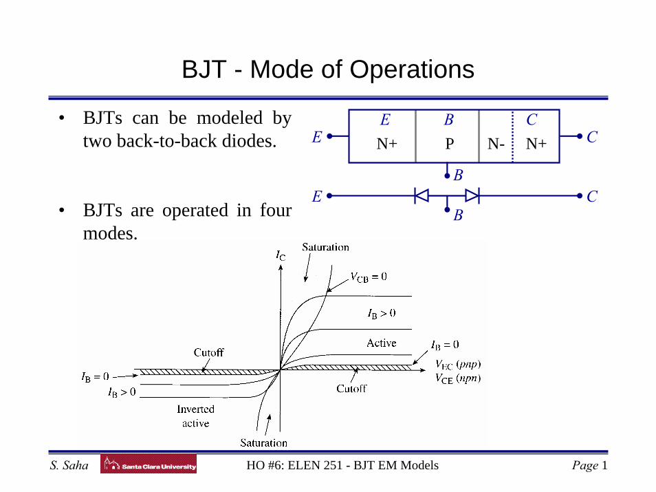
BJT - Mode of Operations HO #6: ELEN 251 - BJT EM Models Page 1 S. Saha N+ P E B C N- N+ E C B B E C • BJTs can be modeled by two back-to-back diodes. • BJTs are operated in four modes.
Transcript of BJT - Mode of Operations - SCU · BJT - Mode of Operations S. Saha HO #6: ELEN 251 - BJT EM Models...
BJT - Mode of Operations
HO #6: ELEN 251 - BJT EM Models Page 1S. Saha
N+ PE B C
N- N+E C
B
BE C
• BJTs can be modeled by two back-to-back diodes.
• BJTs are operated in four modes.

HO #6: ELEN 251 - BJT EM Models Page 2S. Saha
Mode of Operations
1) Forward active / normal– BE junction forward biased– BC junction reversed biased
here,,BFC
BC
IIII
β=∴∝
where βF = forward gain
+ VBC
+ VBE
−
−
Saturation
NormalCut-off
Inverse
2) Reverse active– BE junction reverse biased and BC junction forward biased
here, reverse gain, βR = IE/IB ≈ 1
3) Saturation region– BE and BC are forward biased
4) Cut-off region– BE and BC are reversed biased
Basic BJT Model
HO #6: ELEN 251 - BJT EM Models Page 3S. Saha
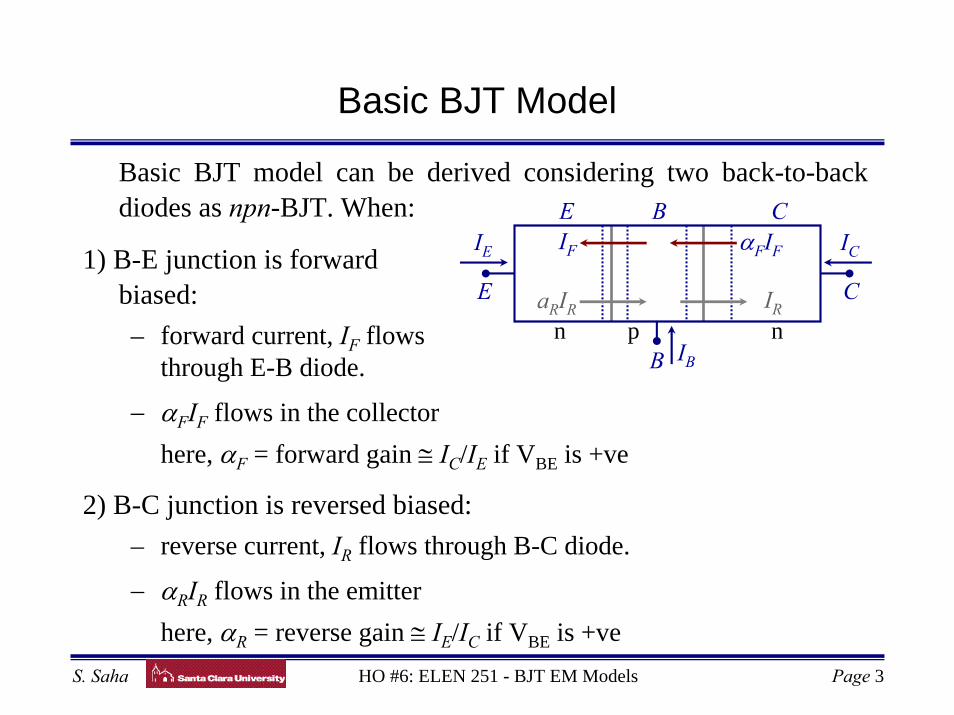
Basic BJT model can be derived considering two back-to-back diodes as npn-BJT. When:
1) B-E junction is forward biased:– forward current, IF flows through E-B diode.
− αFIF flows in the collectorhere, αF = forward gain ≅ IC/IE if VBE is +ve
2) B-C junction is reversed biased:– reverse current, IR flows through B-C diode.
− αRIR flows in the emitterhere, αR = reverse gain ≅ IE/IC if VBE is +ve
n p
E B C
n
E C
IE IC
B IB
IF αFIF
aRIR IR
EM1 BJT Model: Injection Version
HO #6: ELEN 251 - BJT EM Models Page 4S. Saha
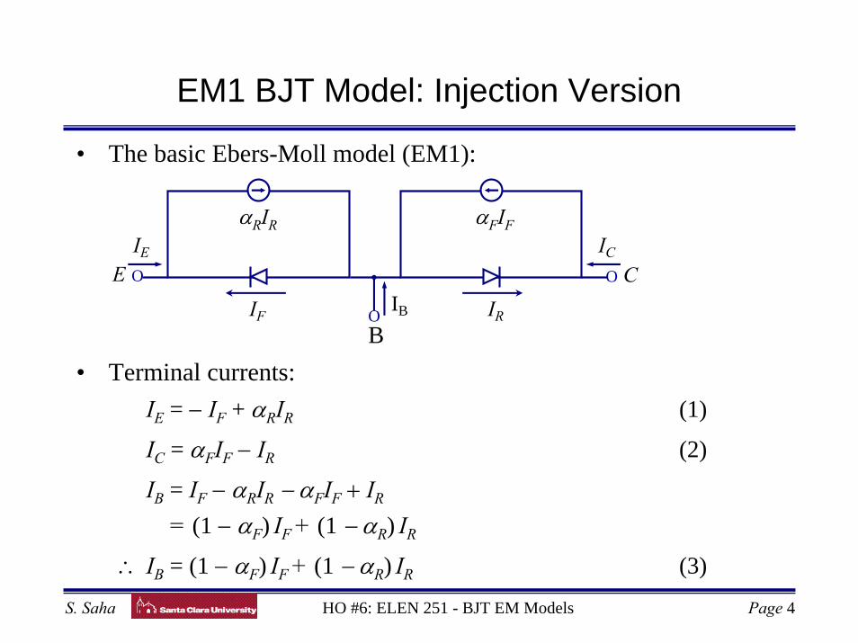
• The basic Ebers-Moll model (EM1):
E O
IE
O CIC
IB
αRIR αFIF
OB
IF IR
• Terminal currents: IE = − IF + αRIR (1)
IC = αFIF − IR (2)
IB = IF − αRIR − αFIF + IR
= (1 − αF) IF + (1 − αR) IR
∴ IB = (1 − αF) IF + (1 − αR) IR (3)
EM1 BJT Model: Injection Version
HO #6: ELEN 251 - BJT EM Models Page 5S. Saha
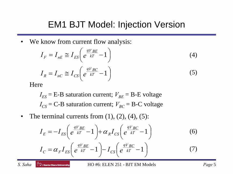
• We know from current flow analysis:
Here IES = E-B saturation current; VBE = B-E voltage ICS = C-B saturation current; VBC = B-C voltage
• The terminal currents from (1), (2), (4), (5):
⎟⎠⎞⎜
⎝⎛ −≅=
⎟⎠⎞⎜
⎝⎛ −≅=
1
1
eIII
eIII
kTV BCq
CSnCR
kTV BEq
ESnEF (4)
(5)
⎟⎠⎞⎜
⎝⎛ −−⎟
⎠⎞⎜
⎝⎛ −=
⎟⎠⎞⎜
⎝⎛ −+⎟
⎠⎞⎜
⎝⎛ −−=
11
11
eIeII
eIeII
kTV BCq
CSkTV BEq
ESFC
kTV BCq
CSRkTV BEq
ESE
α
α (6)
(7)
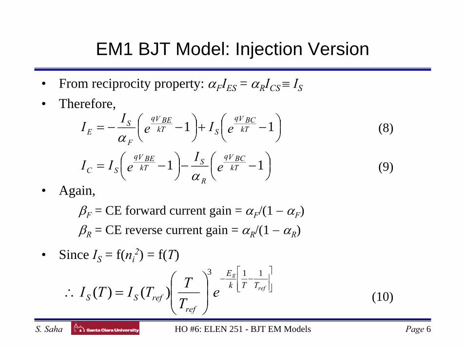
EM1 BJT Model: Injection Version
HO #6: ELEN 251 - BJT EM Models Page 6S. Saha
• From reciprocity property: αFIES = αRICS ≡ IS
• Therefore,
• Again, βF = CE forward current gain = αF/(1 − αF) βR = CE reverse current gain = αR/(1 − αR)
• Since IS = f(ni2) = f(T)
⎟⎠⎞⎜
⎝⎛ −−⎟
⎠⎞⎜
⎝⎛ −=
⎟⎠⎞⎜
⎝⎛ −+⎟
⎠⎞⎜
⎝⎛ −−=
11
11
eI
eII
eIeII
kTV BCq
R
SkT
V BEq
SC
kTV BCq
SkTV BEq
F
SE
α
α(8)
(9)
⎥⎥⎦
⎤
⎢⎢⎣
⎡−−
⎟⎟⎠
⎞⎜⎜⎝
⎛=∴ ref
g
TTkE
refrefSS e
TTTITI
113
)()( (10)
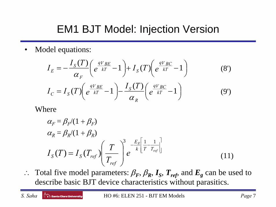
EM1 BJT Model: Injection Version
HO #6: ELEN 251 - BJT EM Models Page 7S. Saha
• Model equations:
Where αF = βF/(1 + βF) αR = βR/(1 + βR)
∴ Total five model parameters: βF, βR, IS, Tref, and Eg can be used to describe basic BJT device characteristics without parasitics.
⎟⎠⎞⎜
⎝⎛ −−⎟
⎠⎞⎜
⎝⎛ −=
⎟⎠⎞⎜
⎝⎛ −+⎟
⎠⎞⎜
⎝⎛ −−=
1)(1)(
1)(1)(
eTI
eTII
eTIeTII
kTV BCq
R
SkT
V BEq
SC
kTV BCq
SkTV BEq
F
SE
α
α(8')
(9')
⎥⎥⎦
⎤
⎢⎢⎣
⎡−−
⎟⎟⎠
⎞⎜⎜⎝
⎛= ref
g
TTkE
refrefSS e
TTTITI
113
)()( (11)
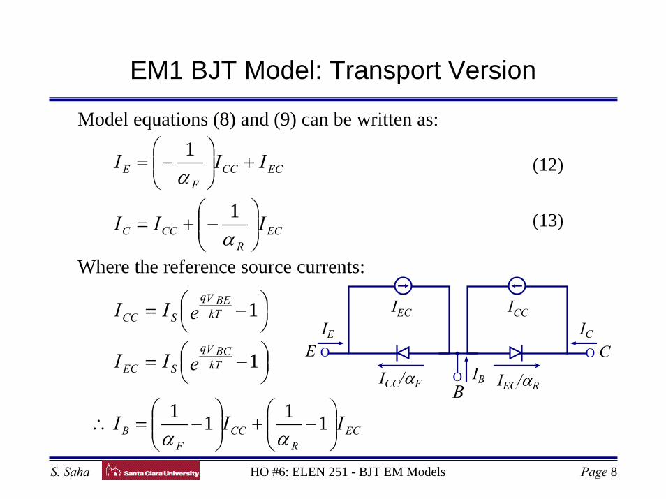
EM1 BJT Model: Transport Version
HO #6: ELEN 251 - BJT EM Models Page 8S. Saha
Model equations (8) and (9) can be written as:
Where the reference source currents:
ECR
CCC
ECCCF
E
III
III
⎟⎟⎠
⎞⎜⎜⎝
⎛−+=
+⎟⎟⎠
⎞⎜⎜⎝
⎛−=
α
α
1
1(12)
(13)
⎟⎠⎞⎜
⎝⎛ −=
⎟⎠⎞⎜
⎝⎛ −=
1
1
eII
eII
kTV BCq
SEC
kTV BEq
SCC
E O
IE
O CIC
IB
IEC ICC
OB
ICC/αF IEC/αR
ECR
CCF
B III ⎟⎟⎠
⎞⎜⎜⎝
⎛−+⎟⎟
⎠
⎞⎜⎜⎝
⎛−=∴ 1111
αα
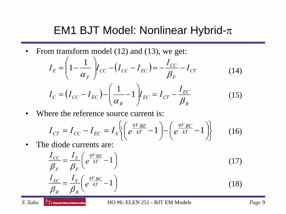
EM1 BJT Model: Nonlinear Hybrid-π
HO #6: ELEN 251 - BJT EM Models Page 9S. Saha
• From transform model (12) and (13), we get:
• Where the reference source current is:
• The diode currents are:
( )
( )R
ECCTEC
RECCCC
CTF
CCECCCCC
FE
IIIIII
IIIIII
βα
βα
−=⎟⎟⎠
⎞⎜⎜⎝
⎛−−−=
−−=−−⎟⎟⎠
⎞⎜⎜⎝
⎛−=
11
11 (14)
(15)
⎭⎬⎫
⎩⎨⎧ ⎟
⎠⎞⎜
⎝⎛ −−⎟
⎠⎞⎜
⎝⎛ −=−= 11 eeIIII kT
V BCqkT
V BEq
SECCCCT (16)
⎟⎠⎞⎜
⎝⎛ −=
⎟⎠⎞⎜
⎝⎛ −=
1
1
eII
eII
kTV BCq
R
S
R
EC
kTV BEq
F
S
F
CC
ββ
ββ(17)
(18)
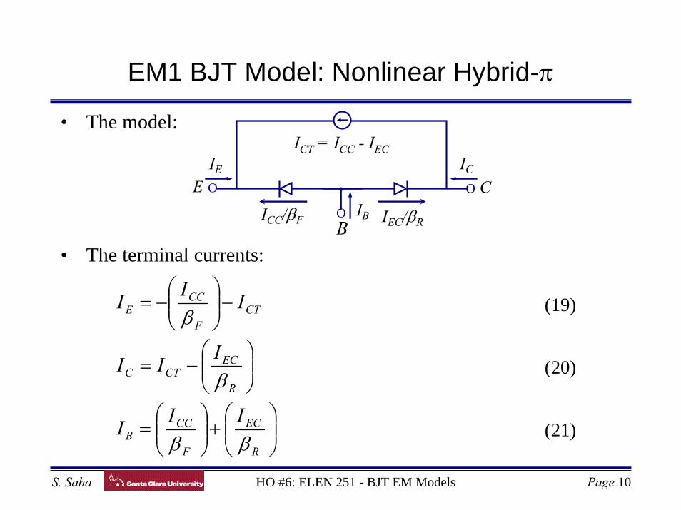
EM1 BJT Model: Nonlinear Hybrid-π
HO #6: ELEN 251 - BJT EM Models Page 10S. Saha
• The model:
• The terminal currents:
E O
IE
O CIC
IB
ICT = ICC - IEC
OB
ICC/βF IEC/βR
⎟⎟⎠
⎞⎜⎜⎝
⎛+⎟⎟
⎠
⎞⎜⎜⎝
⎛=
⎟⎟⎠
⎞⎜⎜⎝
⎛−=
−⎟⎟⎠
⎞⎜⎜⎝
⎛−=
R
EC
F
CCB
R
ECCTC
CTF
CCE
III
III
III
ββ
β
β(19)
(20)
(21)
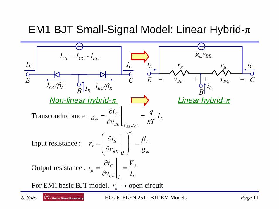
EM1 BJT Small-Signal Model: Linear Hybrid-π
HO #6: ELEN 251 - BJT EM Models Page 11S. Saha
circuitopen model, BJT basic EM1For
:resistanceOutput
:resistanceInput
:ctanceTranscondu
1
),(
→
=∂∂
=
=⎟⎟
⎠
⎞
⎜⎜
⎝
⎛
∂∂
=
=∂∂
=
−
µ
µ
β
r
IV
vir
gvir
IkTq
vig
C
A
QCE
C
m
F
QBE
Bπ
CIVBE
Cm
CBE
OE
iE
OC
iC
iB
gmvBE
OB
− vBE + + vBC −
rµrπ
OE
IE
OC
IC
IB
ICT = ICC - IEC
OB
ICC/βF IEC/βR
Non-linear hybrid-π Linear hybrid-π
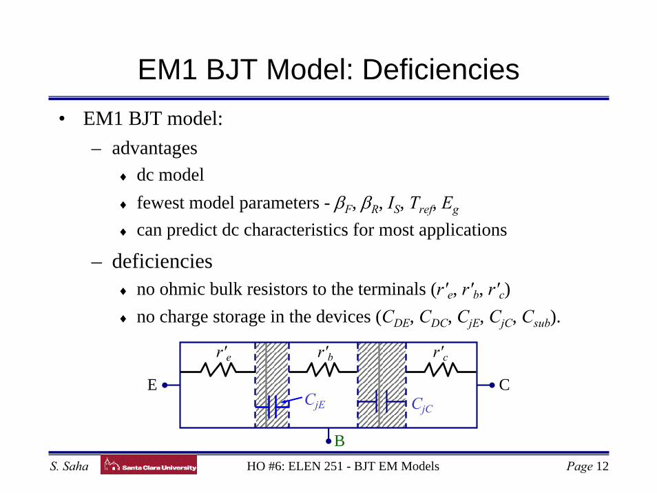
EM1 BJT Model: Deficiencies
HO #6: ELEN 251 - BJT EM Models Page 12S. Saha
• EM1 BJT model:– advantages
♦ dc model♦ fewest model parameters - βF, βR, IS, Tref, Eg
♦ can predict dc characteristics for most applications
– deficiencies♦ no ohmic bulk resistors to the terminals (r'e, r'b, r'c)♦ no charge storage in the devices (CDE, CDC, CjE, CjC, Csub).
E
B
C
r'c
CjE CjC
r'e r'b
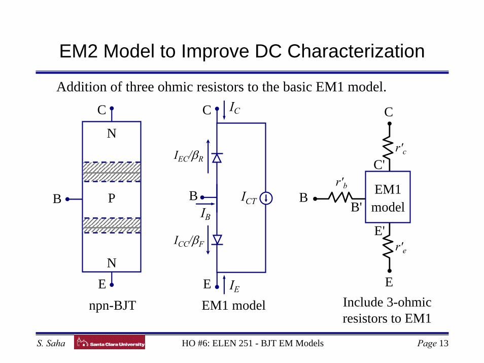
EM2 Model to Improve DC Characterization
HO #6: ELEN 251 - BJT EM Models Page 13S. Saha
Addition of three ohmic resistors to the basic EM1 model.C IC
E IE
IB
ICTB
IEC/βR
ICC/βF
C
B
E
N
P
N
npn-BJT EM1 model Include 3-ohmicresistors to EM1
E
r'c
r'e
r'b EM1model
B
C
B'
C'
E'
Effect of Ohmic Bulk Resistors - r'c
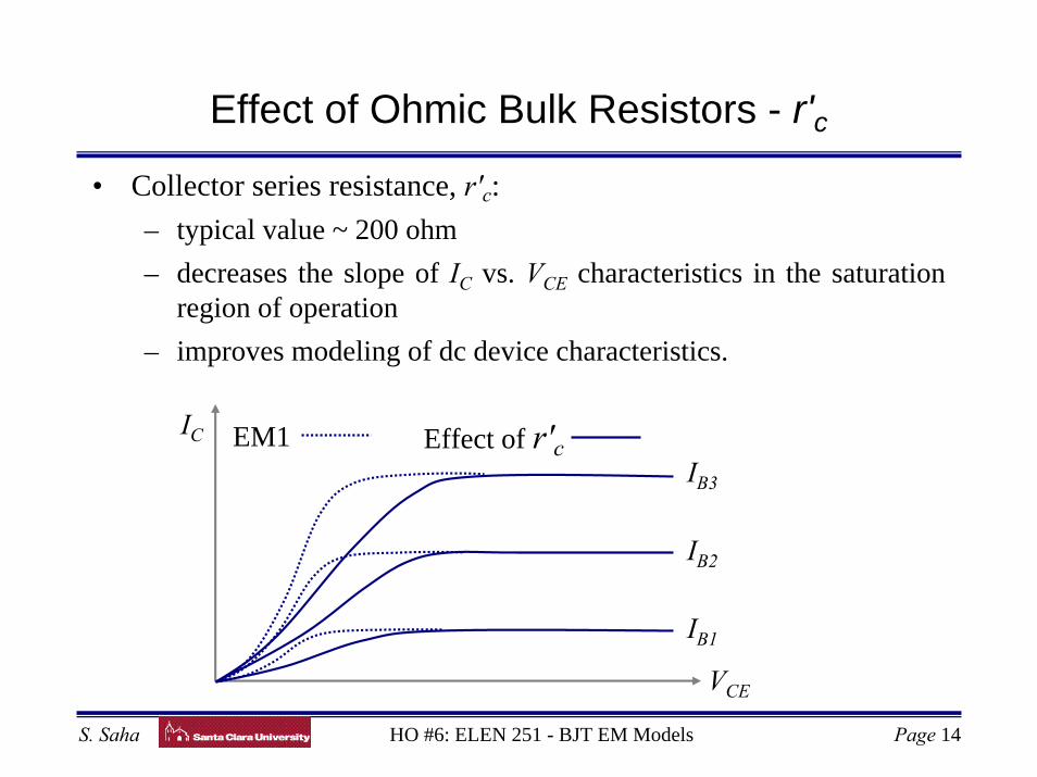
HO #6: ELEN 251 - BJT EM Models Page 14S. Saha
• Collector series resistance, r'c:– typical value ~ 200 ohm– decreases the slope of IC vs. VCE characteristics in the saturation
region of operation– improves modeling of dc device characteristics.
VCE
IC
IB3
IB2
IB1
EM1 Effect of r'c

Effect of Ohmic Bulk Resistors - r'e and r'b
HO #6: ELEN 251 - BJT EM Models Page 15S. Saha
• Emitter series resistance, r'e:– typical value ≈ 5 ohm due to polysilicon contact– reduces EB junction potential by a factor of r'eIE
∆VBE = IEr'e = (IC + IB)r'e = IB(1 + βF)r'e∴ r'e is equivalent to a base resistance of (1 + βF)r'e– effects IC and IB of the device.
VBE
ln(I
C, I
B)IC
IB
∆VBE = IBr'b + IEr'e
• Base series resistance, r'b:– effects small-signal and
transient response– difficult to measure
accurately due to the dependence on r'e and operating point.
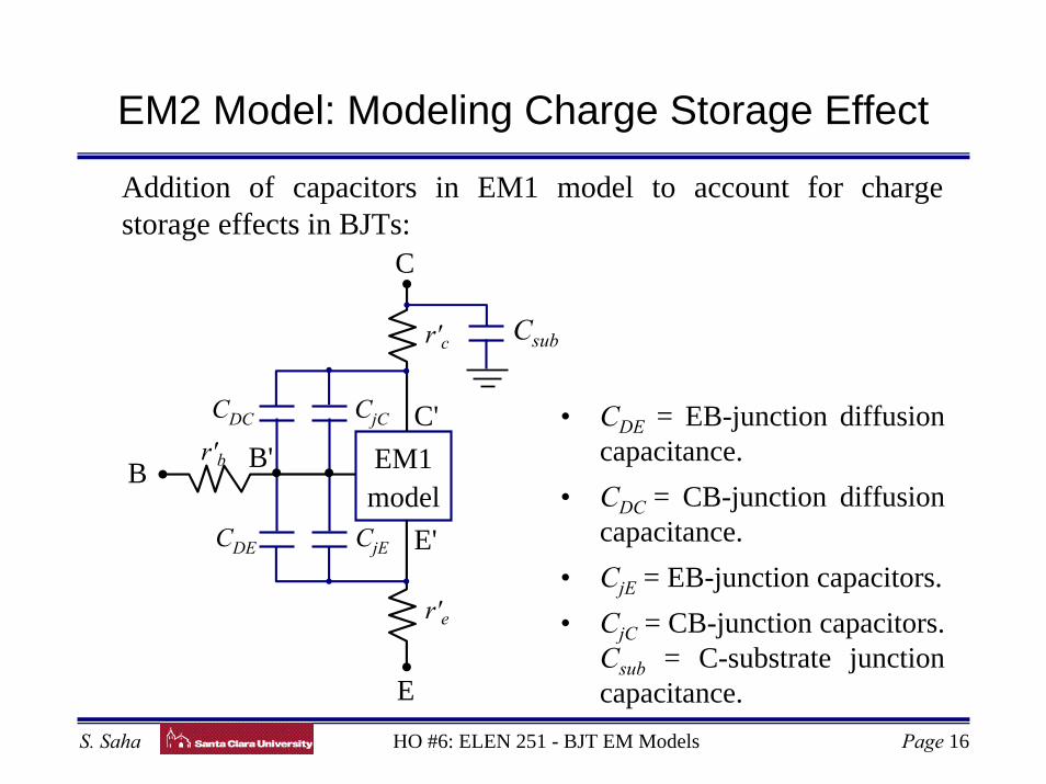
EM2 Model: Modeling Charge Storage Effect
HO #6: ELEN 251 - BJT EM Models Page 16S. Saha
Addition of capacitors in EM1 model to account for charge storage effects in BJTs:
E
r'c
r'e
r'b EM1model
B
C
B'C'
E'
Csub
CjC
CjE
CDC
CDE
• CDE = EB-junction diffusion capacitance.
• CDC = CB-junction diffusion capacitance.
• CjE = EB-junction capacitors.• CjC = CB-junction capacitors.
Csub = C-substrate junction capacitance.
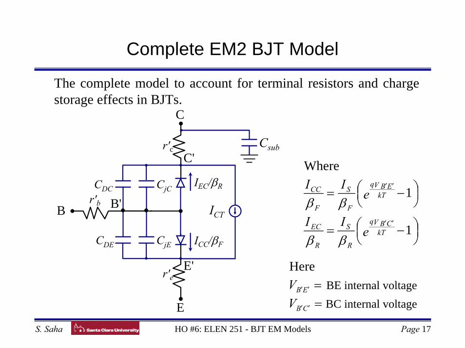
Complete EM2 BJT Model
HO #6: ELEN 251 - BJT EM Models Page 17S. Saha
The complete model to account for terminal resistors and charge storage effects in BJTs.
E
r'c
r'e
r'bB
C
B'
C'
E'
Csub
CjC
CjE
CDC
CDE
ICT
IEC/βR
ICC/βF⎟⎠⎞⎜
⎝⎛ −=
⎟⎠⎞⎜
⎝⎛ −=
′′
′′
1
1
Where
eII
eII
kTV CBq
R
S
R
EC
kTV EBq
F
S
F
CC
ββ
ββ
==
′′
′′
CB
EB
VVHere
BE internal voltageBC internal voltage
EM2 Model: Junction Capacitors
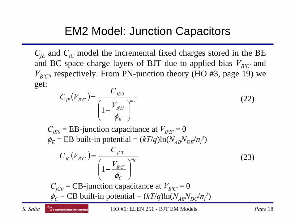
HO #6: ELEN 251 - BJT EM Models Page 18S. Saha
CjE and CjC model the incremental fixed charges stored in the BE and BC space charge layers of BJT due to applied bias VB'E' and VB'C', respectively. From PN-junction theory (HO #3, page 19) we get:
( )Em
E
EB
jEEBjE
V
CVC
⎟⎟⎠
⎞⎜⎜⎝
⎛−
=′′
′′
φ1
0(22)
( )Cm
C
CB
jCCBjC
V
CVC
⎟⎟⎠
⎞⎜⎜⎝
⎛−
=′′
′′
φ1
0(23)
CjE0 = EB-junction capacitance at VB'E' = 0 φE = EB built-in potential = (kT/q)ln(NABNDE/ni
2)
CjC0 = CB-junction capacitance at VB'C' = 0 φC = CB built-in potential = (kT/q)ln(NABNDC/ni
2)
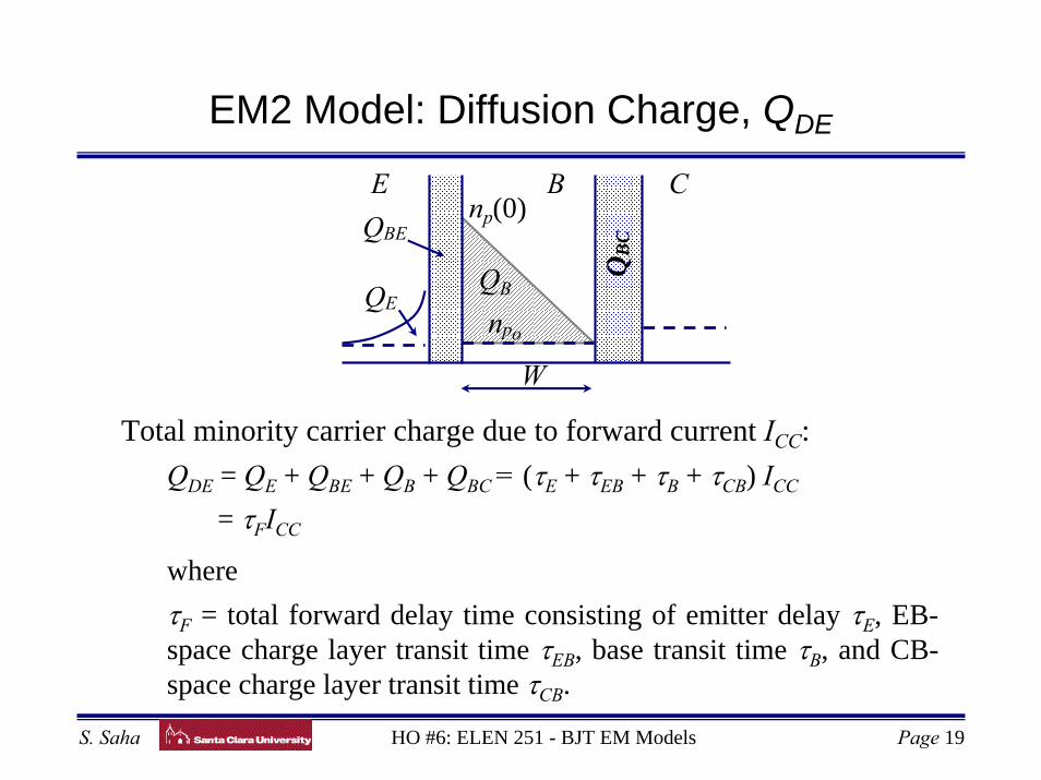
EM2 Model: Diffusion Charge, QDE
HO #6: ELEN 251 - BJT EM Models Page 19S. Saha
E Cnp(0)
npo
B
QBQE
QB
CQBE
W
Total minority carrier charge due to forward current ICC: QDE = QE + QBE + QB + QBC = (τE + τEB + τB + τCB) ICC
= τFICC
where τF = total forward delay time consisting of emitter delay τE, EB-
space charge layer transit time τEB, base transit time τB, and CB-space charge layer transit time τCB.
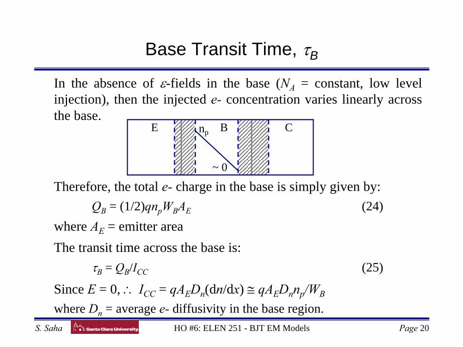
Base Transit Time, τB
HO #6: ELEN 251 - BJT EM Models Page 20S. Saha
In the absence of ε-fields in the base (NA = constant, low level injection), then the injected e- concentration varies linearly across the base.
Therefore, the total e- charge in the base is simply given by: QB = (1/2)qnpWBAE (24)
where AE = emitter area The transit time across the base is:
τB = QB/ICC (25)
Since E = 0, ∴ ICC = qAEDn(dn/dx) ≅ qAEDnnp/WB
where Dn = average e- diffusivity in the base region.
npE B C
~ 0
Base Transit Time
HO #6: ELEN 251 - BJT EM Models Page 21S. Saha
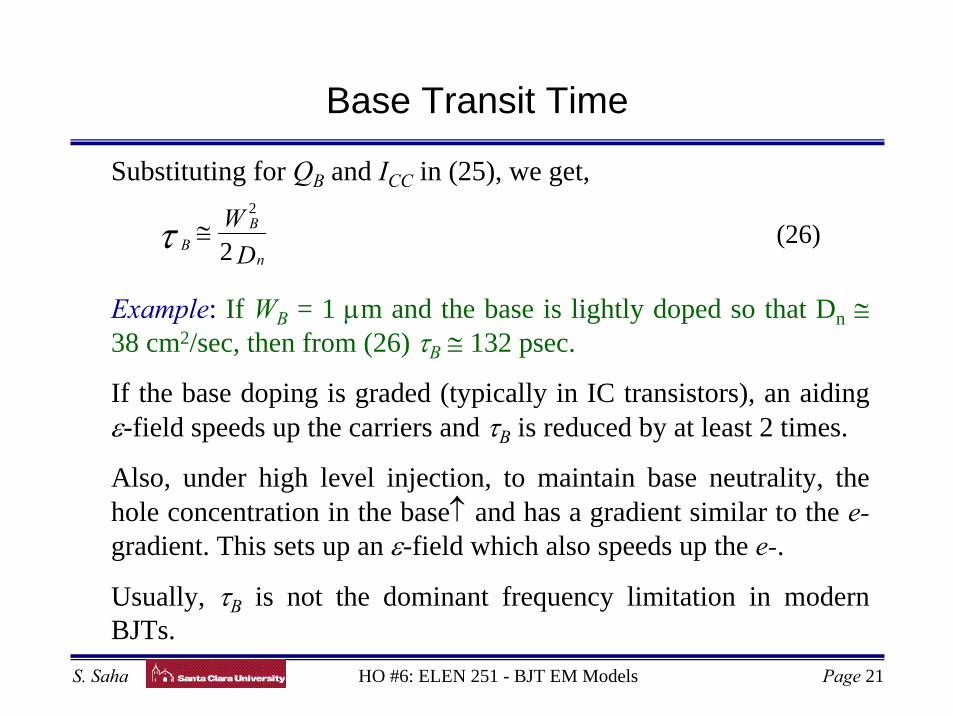
Substituting for QB and ICC in (25), we get,
Example: If WB = 1 µm and the base is lightly doped so that Dn ≅38 cm2/sec, then from (26) τB ≅ 132 psec.
If the base doping is graded (typically in IC transistors), an aiding ε-field speeds up the carriers and τB is reduced by at least 2 times.
Also, under high level injection, to maintain base neutrality, the hole concentration in the base↑ and has a gradient similar to the e-gradient. This sets up an ε-field which also speeds up the e-.
Usually, τB is not the dominant frequency limitation in modern BJTs.
DW
n
BB 2
2
≅τ (26)
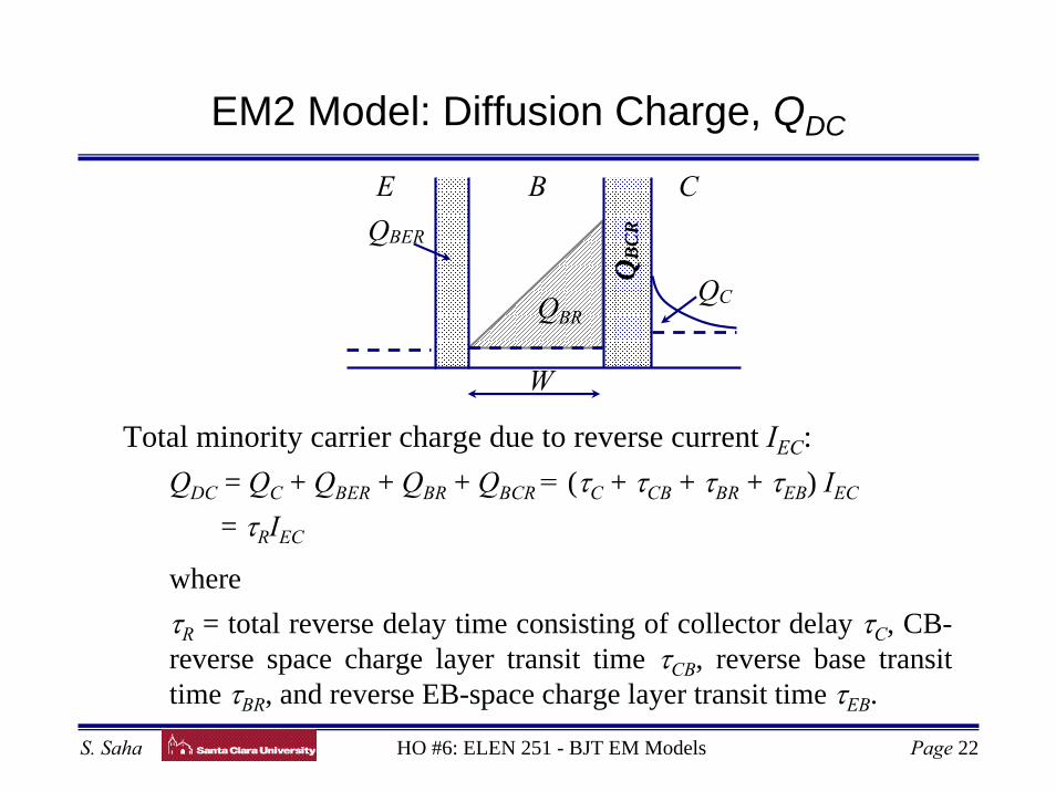
EM2 Model: Diffusion Charge, QDC
HO #6: ELEN 251 - BJT EM Models Page 22S. Saha
E CB
QBRQC
QB
CRQBER
W
Total minority carrier charge due to reverse current IEC: QDC = QC + QBER + QBR + QBCR = (τC + τCB + τBR + τEB) IEC
= τRIEC
where τR = total reverse delay time consisting of collector delay τC, CB-
reverse space charge layer transit time τCB, reverse base transit time τBR, and reverse EB-space charge layer transit time τEB.
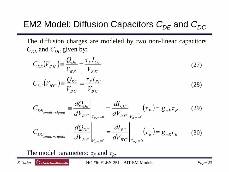
EM2 Model: Diffusion Capacitors CDE and CDC
HO #6: ELEN 251 - BJT EM Models Page 23S. Saha
The diffusion charges are modeled by two non-linear capacitors CDE and CDC given by:
( )
( )CB
ECR
CB
DCCBDC
EB
CCF
EB
DEEBDE
VI
VQVC
VI
VQVC
′′′′′′
′′′′′′
=≡
=≡
τ
τ(27)
(28)
( )
( ) RmRRVCB
EC
VCB
DCsignalsmallDC
FmFFVEB
CC
VEB
DEsignalsmallDE
gdVdI
dVdQC
gdVdI
dVdQC
EBEB
CBCB
ττ
ττ
==≡
==≡
=′′=′′−
=′′=′′−
′′′′
′′′′
00
00
(29)
(30)
The model parameters: τF and τR.
EM2 Model: Model Parameters
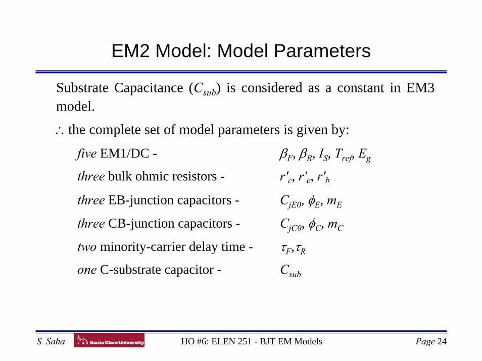
HO #6: ELEN 251 - BJT EM Models Page 24S. Saha
Substrate Capacitance (Csub) is considered as a constant in EM3 model.
∴the complete set of model parameters is given by:
five EM1/DC - βF, βR, IS, Tref, Eg
three bulk ohmic resistors - r'c, r'e, r'b three EB-junction capacitors - CjE0, φE, mE
three CB-junction capacitors - CjC0, φC, mC
two minority-carrier delay time - τF,τR
one C-substrate capacitor - Csub

EM2 Model: Discussions
HO #6: ELEN 251 - BJT EM Models Page 25S. Saha
• Advantages of EM2 model is the improvement in DC and AC device characterization over EM1 model by addition of:– bulk ohmic resistors– charge storage in the devices
• The limitations of EM2 model are:– base-width modulation
– variation of β with current level– distributed collector capacitance– variation of device parameters with temperature
– high current effect on τF.
• New model parameters are added to EM2 BJT model to improve device characterization ⇒ EM3 BJT model.
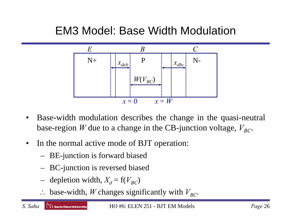
EM3 Model: Base Width Modulation
HO #6: ELEN 251 - BJT EM Models Page 26S. Saha
BE C
W(VBC)
N+ P N-xdbcxdeb
x = 0 x = W
• Base-width modulation describes the change in the quasi-neutral base-region W due to a change in the CB-junction voltage, VBC.
• In the normal active mode of BJT operation:– BE-junction is forward biased– BC-junction is reversed biased– depletion width, Xd = f(VBC)∴ base-width, W changes significantly with VBC.
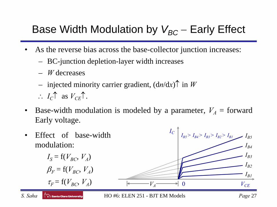
Base Width Modulation by VBC − Early Effect
HO #6: ELEN 251 - BJT EM Models Page 27S. Saha
• As the reverse bias across the base-collector junction increases:– BC-junction depletion-layer width increases– W decreases– injected minority carrier gradient, (dn/dx)↑ in W∴ IC↑ as VCE↑.
• Base-width modulation is modeled by a parameter, VA = forward Early voltage.
IB5
IB4
IB3
IB2
IB1
VA VCE
IC IB5 > IB4 > IB3 > IB2 > IB1
0
• Effect of base-width modulation:
IS = f(VBC, VA)
βF = f(VBC, VA)τF = f(VBC, VA)
Base Width Modulation
HO #6: ELEN 251 - BJT EM Models Page 28S. Saha
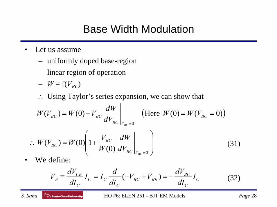
• Let us assume– uniformly doped base-region– linear region of operation– W = f(VBC)∴ Using Taylor’s series expansion, we can show that
• We define:
( )
⎟⎟
⎠
⎞
⎜⎜
⎝
⎛+=∴
==+=
=
=
0
0
)0(1)0()(
)0()0( Here )0()(
BC
BC
VBC
BCBC
BCVBC
BCBC
dVdW
WVWVW
VWWdVdWVWVW
(31)
CC
BCBEBC
CCC
C
CEA I
dIdVVV
dIdII
dIdVV −=+−=≡ )( (32)

Base Width Modulation
HO #6: ELEN 251 - BJT EM Models Page 29S. Saha
Now,
From (32) and (33):
Combining (31) and (34) we get:
)0(WdW
dVVBCV
BCA −= (34)
(33)0
0
2
)0()0(
)(
=
=
=−⇒−=∴
−≅
BC
BC
kTBE
VC
CCC
V
Vq
BCAB
inBC
dWW
dIIdW
WIdI
eVWNnDqAI
⎟⎟⎠
⎞⎜⎜⎝
⎛+=
A
BCBC V
VWVW 1)0()( (35)
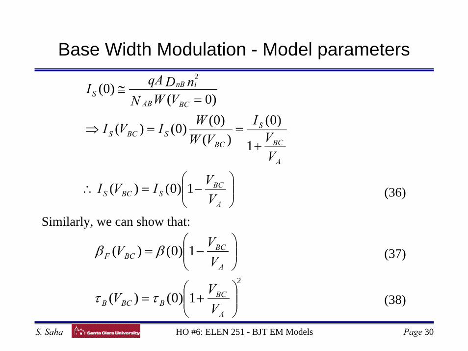
Base Width Modulation - Model parameters
HO #6: ELEN 251 - BJT EM Models Page 30S. Saha
(36)⎟⎟⎠
⎞⎜⎜⎝
⎛−=∴
+==⇒
=≅
A
BCSBCS
A
BC
S
BCSBCS
BCAB
inBS
VVIVI
VV
IVW
WIVI
VWNnDqAI
1)0()(
1
)0()(
)0()0()(
)0()0(
2
Similarly, we can show that:
2
1)0()(
1)0()(
⎟⎟⎠
⎞⎜⎜⎝
⎛+=
⎟⎟⎠
⎞⎜⎜⎝
⎛−=
A
BCBBCB
A
BCBCF
VVV
VVV
ττ
ββ (37)
(38)

Base Width Modulation
HO #6: ELEN 251 - BJT EM Models Page 31S. Saha
• The base-width modulation model parameter, VA:– does not change the equivalent circuits– changes the terminal current equations over EM1/EM2 models.
• The expression for current source:
• VA is measured from the slope of IC vs. VCE characteristic in the active region of BJT operation. slope = (dIC/dVCE)|VBE = constant = −(dIC/dVBC)|VBE = constant
⎭⎬⎫
⎩⎨⎧ ⎟
⎠⎞⎜
⎝⎛ −−⎟
⎠⎞⎜
⎝⎛ −
⎟⎟⎠
⎞⎜⎜⎝
⎛+
= 111
)0(ee
VV
II kTV BCq
kTV BEq
A
BC
SCT (39)
⎟⎠⎞⎜
⎝⎛ −+⎟
⎠⎞⎜
⎝⎛ −= 1
)0()0(1
)0()0(
eI
eII kT
BCkT
BE Vq
R
SVq
F
SB ββ
(40)
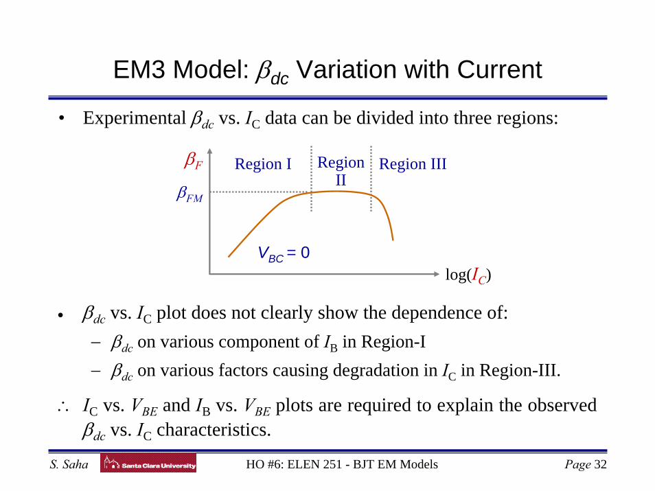
EM3 Model: βdc Variation with Current
HO #6: ELEN 251 - BJT EM Models Page 32S. Saha
• Experimental βdc vs. IC data can be divided into three regions:
Region I RegionII
Region III
log(IC)
βF
βFM
VBC = 0
• βdc vs. IC plot does not clearly show the dependence of:− βdc on various component of IB in Region-I− βdc on various factors causing degradation in IC in Region-III.
∴ IC vs. VBE and IB vs. VBE plots are required to explain the observed βdc vs. IC characteristics.
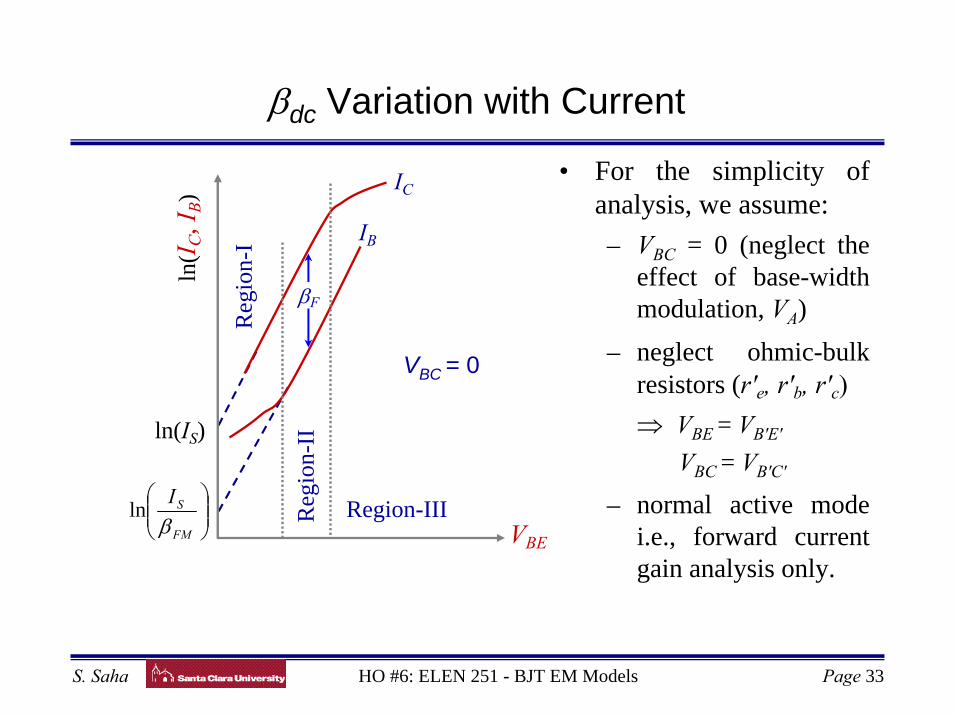
βdc Variation with Current
HO #6: ELEN 251 - BJT EM Models Page 33S. Saha
• For the simplicity of analysis, we assume:– VBC = 0 (neglect the
effect of base-width modulation, VA)
– neglect ohmic-bulk resistors (r'e, r'b, r'c)
⇒ VBE = VB'E'
VBC = VB'C'
– normal active mode i.e., forward current gain analysis only.
ln(I C
, IB)
VBE
IB
IC
βF
Reg
ion-
I
Reg
ion-
II
Region-III
VBC = 0
ln(IS)
⎟⎟⎠
⎞⎜⎜⎝
⎛
FM
SIβ
ln
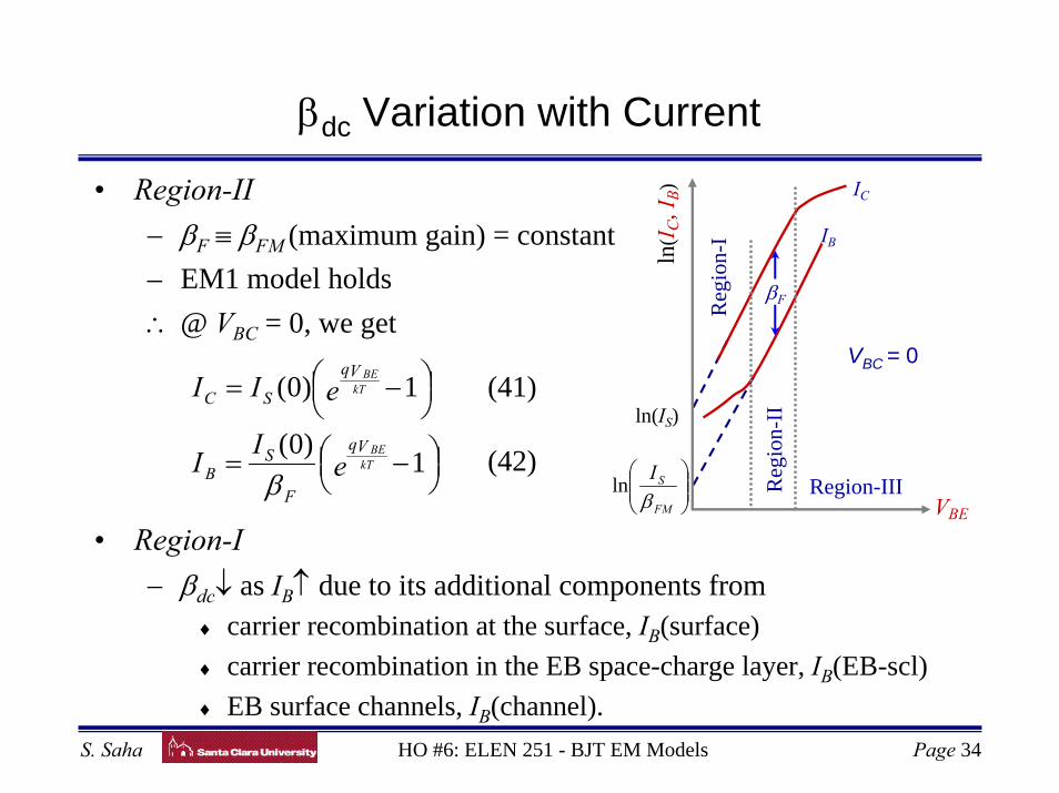
βdc Variation with Current
HO #6: ELEN 251 - BJT EM Models Page 34S. Saha
• Region-II− βF ≡ βFM (maximum gain) = constant – EM1 model holds∴ @ VBC = 0, we get
• Region-I− βdc↓ as IB↑ due to its additional components from
♦ carrier recombination at the surface, IB(surface)♦ carrier recombination in the EB space-charge layer, IB(EB-scl)♦ EB surface channels, IB(channel).
ln(I C
, IB)
VBE
IB
IC
βFReg
ion-
I
Reg
ion-
II
Region-III
VBC = 0
ln(IS)
⎟⎟⎠
⎞⎜⎜⎝
⎛
FM
SIβ
ln⎟⎠⎞⎜
⎝⎛ −=
⎟⎠⎞⎜
⎝⎛ −=
1)0(
1)0(
eII
eII
kTBE
kTBE
Vq
F
SB
Vq
SC
β
(41)
(42)
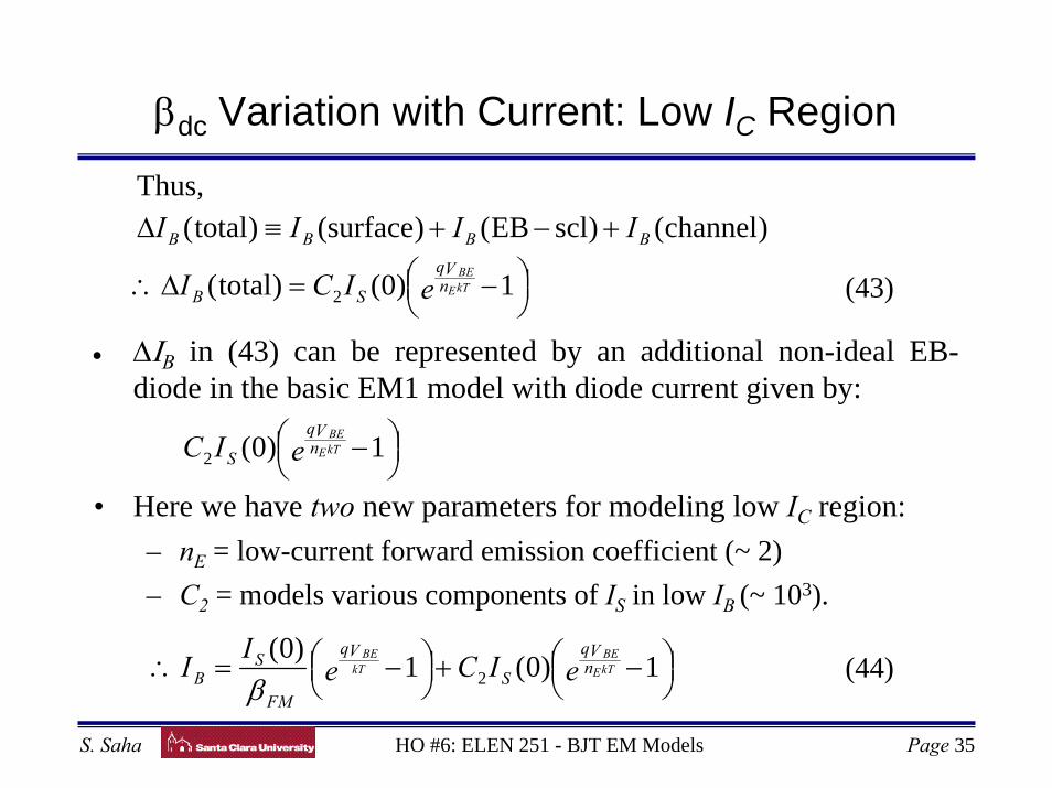
βdc Variation with Current: Low IC Region
HO #6: ELEN 251 - BJT EM Models Page 35S. Saha
• ∆ΙB in (43) can be represented by an additional non-ideal EB-diode in the basic EM1 model with diode current given by:
• Here we have two new parameters for modeling low IC region:– nE = low-current forward emission coefficient (~ 2)– C2 = models various components of IS in low IB (~ 103).
⎟⎠⎞⎜
⎝⎛ −=∆∴
+−+≡∆
1)0()total(
)channel()sclEB()surface()total(Thus,
2 eICI
IIII
kTEBE
nVq
SB
BBBB
⎟⎠⎞⎜
⎝⎛ −1)0(2 eIC kTE
BEnVq
S
(43)
⎟⎠⎞⎜
⎝⎛ −+⎟
⎠⎞⎜
⎝⎛ −=∴ 1)0(1)0(
2 eICeII kTE
BEkT
BEnVq
SVq
FM
SB β
(44)
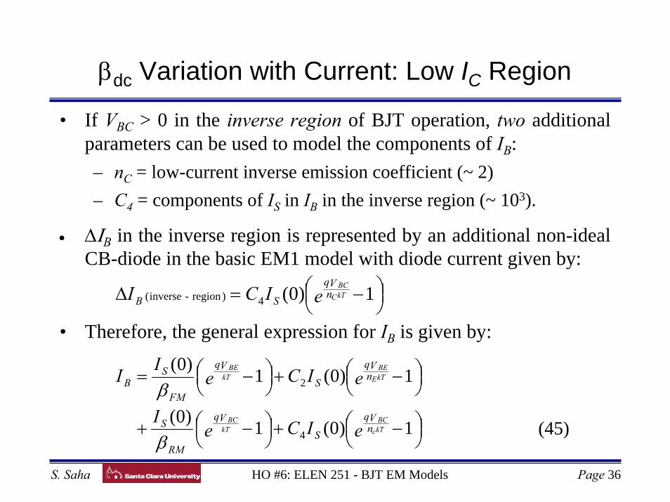
βdc Variation with Current: Low IC Region
HO #6: ELEN 251 - BJT EM Models Page 36S. Saha
• If VBC > 0 in the inverse region of BJT operation, two additional parameters can be used to model the components of IB:– nC = low-current inverse emission coefficient (~ 2)– C4 = components of IS in IB in the inverse region (~ 103).
• ∆ΙB in the inverse region is represented by an additional non-ideal CB-diode in the basic EM1 model with diode current given by:
• Therefore, the general expression for IB is given by:
⎟⎠⎞⎜
⎝⎛ −=∆ 1)0(4)region-inverse( eICI kTC
BCnVq
SB
⎟⎠⎞⎜
⎝⎛ −+⎟
⎠⎞⎜
⎝⎛ −+
⎟⎠⎞⎜
⎝⎛ −+⎟
⎠⎞⎜
⎝⎛ −=
1)0(1)0(
1)0(1)0(
4
2
eICeI
eICeII
kTcBC
kTBC
kTEBE
kTBE
nVq
SVq
RM
S
nVq
SVq
FM
SB
β
β
(45)
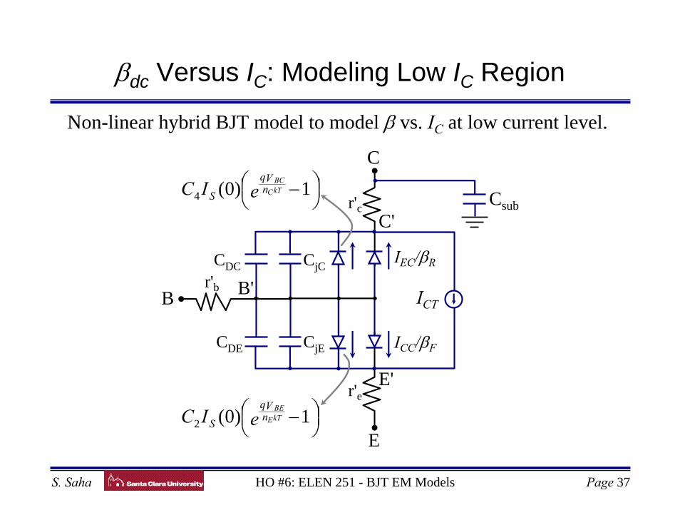
βdc Versus IC: Modeling Low IC Region
HO #6: ELEN 251 - BJT EM Models Page 37S. Saha
Non-linear hybrid BJT model to model β vs. IC at low current level.
E
r'c
r'e
C
C'
E'
Csub
r'bB B'
CjC
CjE
CDC
CDE
ICT
IEC/βR
ICC/βF
⎟⎠⎞⎜
⎝⎛ −1)0(2 eIC kTE
BEnVq
S
⎟⎠⎞⎜
⎝⎛ −1)0(4 eIC kTC
BCnVq
S
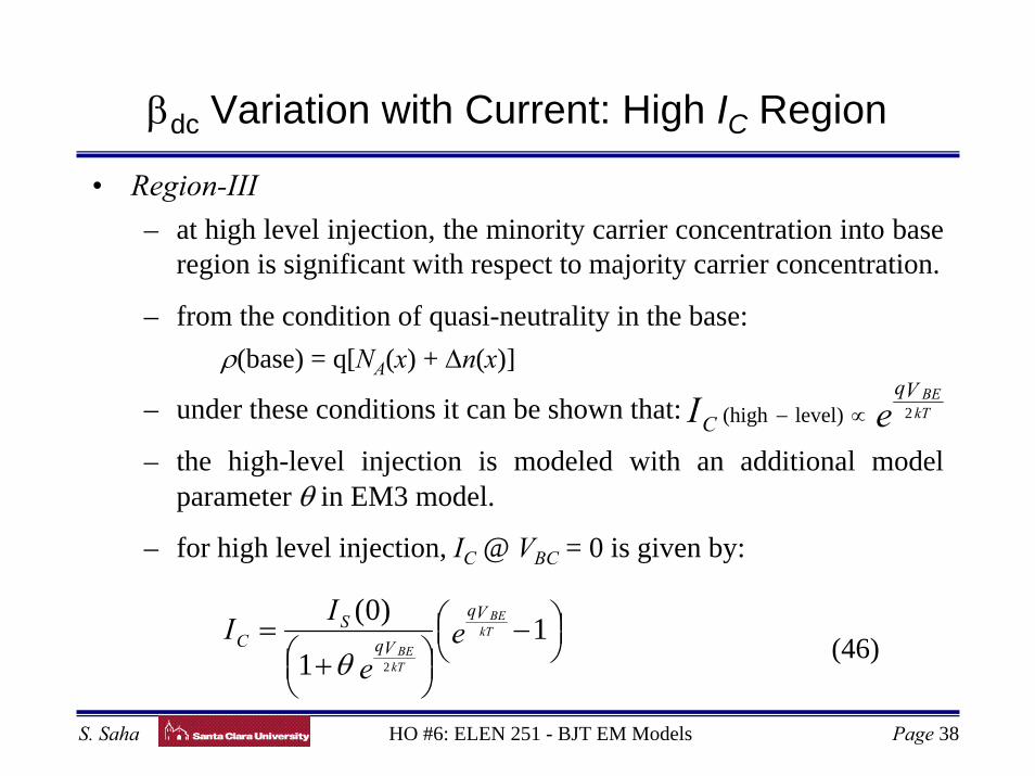
βdc Variation with Current: High IC Region
HO #6: ELEN 251 - BJT EM Models Page 38S. Saha
• Region-III– at high level injection, the minority carrier concentration into base
region is significant with respect to majority carrier concentration.
– from the condition of quasi-neutrality in the base: ρ(base) = q[NA(x) + ∆n(x)]
– under these conditions it can be shown that:
– the high-level injection is modeled with an additional model parameter θ in EM3 model.
– for high level injection, IC @ VBC = 0 is given by:
eI kTBEVq
C 2level)(high ∝−
⎟⎠⎞⎜
⎝⎛ −
⎟⎠⎞⎜
⎝⎛ +
= 11
)0(
2
ee
II kTBE
kTBE
Vq
VqS
Cθ (46)
βdc Variation with Current: Model Parameters
HO #6: ELEN 251 - BJT EM Models Page 39S. Saha
ln(I)
qVBE/kT
IB
IC
βF
VBC = 0
ln(IS(0))
⎟⎟⎠
⎞⎜⎜⎝
⎛
FM
SIβ
)0(ln
ln(C2IS(0))
⎟⎠⎞
⎜⎝⎛
θ)0(ln SI
slope = 1slope = 1
slope = 1/nE
slope = 1/2• EM3-Model parameters
to describe βF - IC data:– Region-I
♦ C2
♦ nE
– Region-II♦ βFM
– Region-III♦ θ
• The parameter set {C2, nE, βFM, θ} is obtained from above plot.• In the inverse region a set {C4, nC, βRM, θR} is defined at VBE = 0.
βdc Versus IC: Effect of Ohmic Resistors
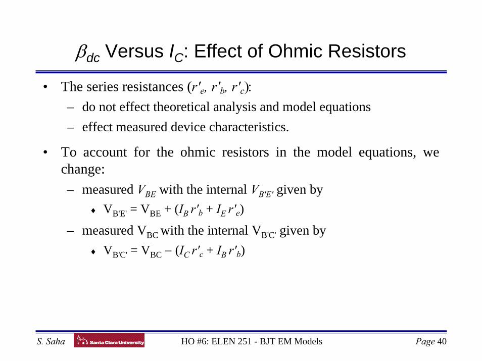
HO #6: ELEN 251 - BJT EM Models Page 40S. Saha
• The series resistances (r'e, r'b, r'c):– do not effect theoretical analysis and model equations– effect measured device characteristics.
• To account for the ohmic resistors in the model equations, we change:– measured VBE with the internal VB'E' given by
♦ VB'E' = VBE + (IB r'b + IE r'e)
– measured VBC with the internal VB'C' given by♦ VB'C' = VBC − (IC r'c + IB r'b)
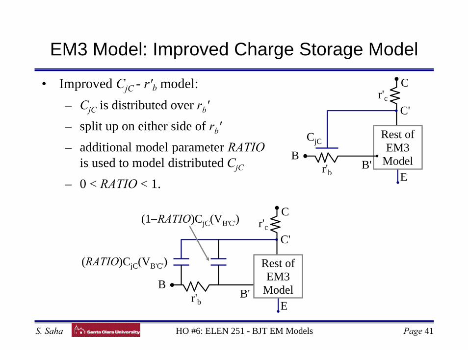
EM3 Model: Improved Charge Storage Model
HO #6: ELEN 251 - BJT EM Models Page 41S. Saha
• Improved CjC - r'b model: – CjC is distributed over rb'– split up on either side of rb'– additional model parameter RATIO
is used to model distributed CjC
– 0 < RATIO < 1. E
r'cC
C'
r'bB
B'
CjCRest ofEM3
Model
E
r'cC
C'
r'bB
B'
(RATIO)CjC(VB'C') Rest ofEM3
Model
(1−RATIO)CjC(VB'C')
EM3 Model: Variation of τF with IC
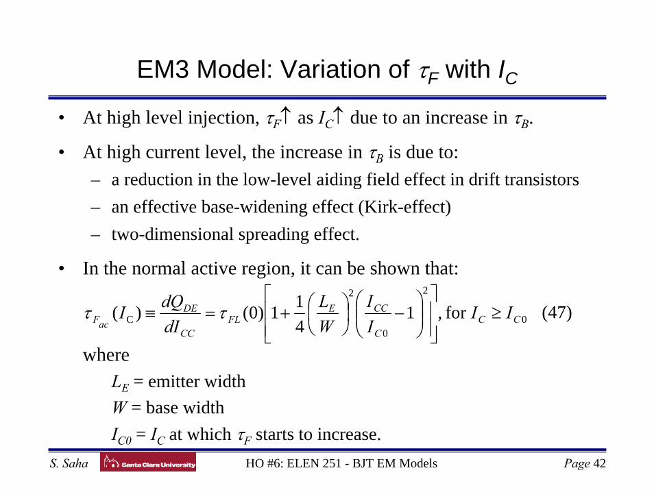
HO #6: ELEN 251 - BJT EM Models Page 42S. Saha
• At high level injection, τF↑ as IC↑ due to an increase in τB.
• At high current level, the increase in τB is due to:– a reduction in the low-level aiding field effect in drift transistors– an effective base-widening effect (Kirk-effect)– two-dimensional spreading effect.
• In the normal active region, it can be shown that:
where LE = emitter width W = base width IC0 = IC at which τF starts to increase.
0
2
0
2
C for ,1411)0()( CC
C
CCEFL
CC
DEacF II
II
WL
dIdQI ≥
⎥⎥⎦
⎤
⎢⎢⎣
⎡⎟⎟⎠
⎞⎜⎜⎝
⎛−⎟
⎠⎞
⎜⎝⎛+=≡ ττ (47)
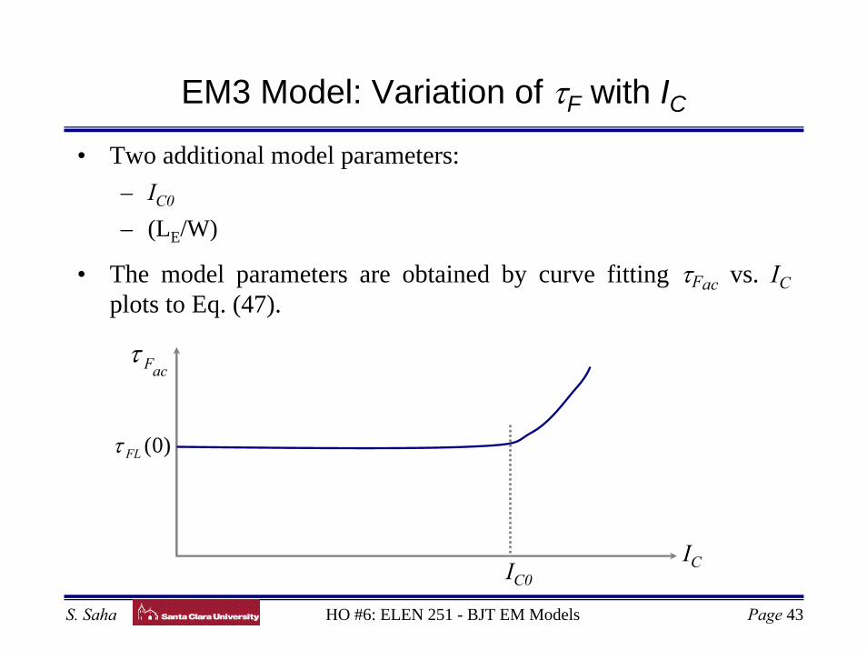
EM3 Model: Variation of τF with IC
HO #6: ELEN 251 - BJT EM Models Page 43S. Saha
• Two additional model parameters:– IC0
– (LE/W)
• The model parameters are obtained by curve fitting τFac vs. ICplots to Eq. (47).
ICIC0
acFτ
)0(FLτ
EM3 Model: Temperature Dependence
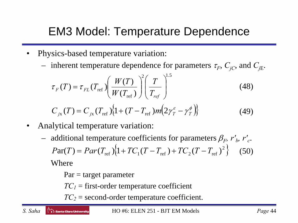
HO #6: ELEN 251 - BJT EM Models Page 44S. Saha
• Physics-based temperature variation: – inherent temperature dependence for parameters τF, CjC, and CjE.
• Analytical temperature variation: – additional temperature coefficients for parameters βF, r'b, r'c.
Where Par = target parameter TC1 = first-order temperature coefficient TC2 = second-order temperature coefficient.
5.12
refref )(
)()()( ⎟⎟⎠
⎞⎜⎜⎝
⎛⎟⎟⎠
⎞⎜⎜⎝
⎛=
refFLF T
TTWTWTT ττ (48)
( ){ }φε γγ TTjj mTTTCTC −−+= 2)(1)()( refrefxx (49)
{ }2ref2ref1ref )()(1)()ar( TTTCTTTCTParTP −+−+= (50)
EM3 Model: Summary
HO #6: ELEN 251 - BJT EM Models Page 45S. Saha
• Additional model parameters – base-width modulation:
♦ VA
− β roll-off:♦ {C2, nE, βFM, θ} (inverse region: {C4, nC, βRM, θR})
– distributed CjC:
♦ RATIO, IC0, LE/W
– temperature coefficients for βF, r'b, r'c:♦ TC1
♦ TC2.
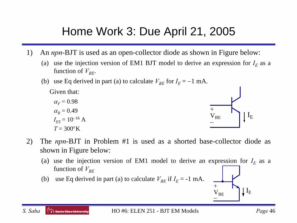
Home Work 3: Due April 21, 2005
HO #6: ELEN 251 - BJT EM Models Page 46S. Saha
1) An npn-BJT is used as an open-collector diode as shown in Figure below:(a) use the injection version of EM1 BJT model to derive an expression for IE as a
function of VBE.(b) use Eq derived in part (a) to calculate VBE for IE = −1 mA.
Given that:αF = 0.98αR = 0.49IES = 10−16 AT = 300°K
2) The npn-BJT in Problem #1 is used as a shorted base-collector diode as shown in Figure below:(a) use the injection version of EM1 model to derive an expression for IE as a
function of VBE
(b) use Eq derived in part (a) to calculate VBE if IE = -1 mA.
+VBE−
IE
+VBE−
IE

Home Work 3: Due April 21, 2005
HO #6: ELEN 251 - BJT EM Models Page 47S. Saha
3) The EM1 model discussed in class can be simplified for different modes of operation. As an example, in the forward active mode, IR is negligibly small and therefore, the model can be simplified for hand calculation. Use the injection version of EM1 model to:(a) show the simplified model in the normal active mode of an npn-BJT operation.(b) show the simplified model in the saturation mode of an npn-BJT operation.
Clearly state any assumptions you make.
4) Following the procedure discussed in class, derive the models for lateral pnp-BJTs:(a) sketch the basic EM1 model(b) write Eq for terminal currents(c) include bulk-ohmic resistors and charge storage elements in EM1 model to
generate lateral pnp-BJT EM2 model.
5) Develop and sketch small-signal linear hybrid-π EM2 model for npn-BJTs. Derive the model equations.