
EM1 BJT Model: Deficiencies - SCU · device characterization ⇒ EM3 BJT model. 29-Jan-04 HO #7:...
34
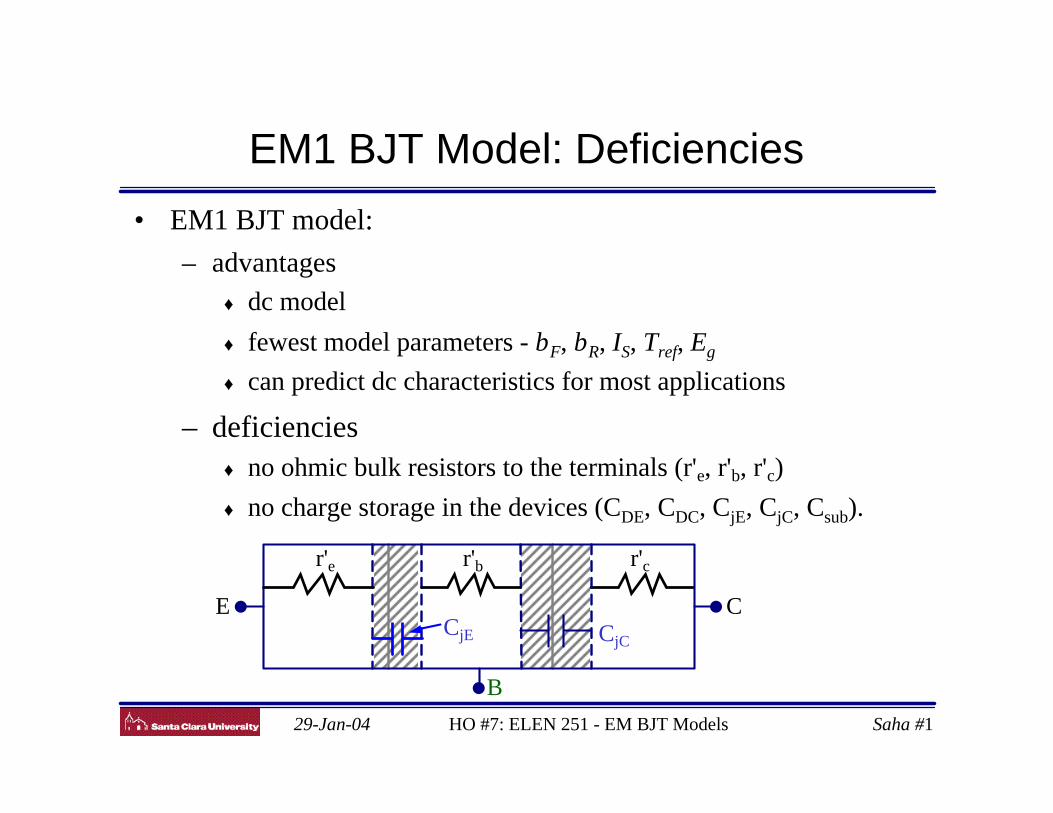
29-Jan-04 HO #7: ELEN 251 - EM BJT Models Saha #1 EM1 BJT Model: Deficiencies • EM1 BJT model: – advantages ♦ dc model ♦ fewest model parameters - b F , b R , I S , T ref , E g ♦ can predict dc characteristics for most applications – deficiencies ♦ no ohmic bulk resistors to the terminals (r' e , r' b , r' c ) ♦ no charge storage in the devices (C DE , C DC , C jE , C jC , C sub ). E B C r' c C jE C jC r' e r' b
Transcript of EM1 BJT Model: Deficiencies - SCU · device characterization ⇒ EM3 BJT model. 29-Jan-04 HO #7:...
29-Jan-04 HO #7: ELEN 251 - EM BJT Models Saha #1
EM1 BJT Model: Deficiencies
• EM1 BJT model:– advantages
♦ dc model
♦ fewest model parameters - βF, βR, IS, Tref, Eg
♦ can predict dc characteristics for most applications
– deficiencies♦ no ohmic bulk resistors to the terminals (r'e, r'b, r'c)♦ no charge storage in the devices (CDE, CDC, CjE, CjC, Csub).
E
B
C
r'c
CjE CjC
r'e r'b
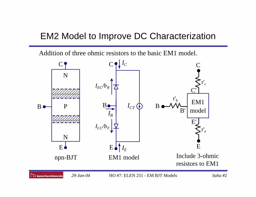
29-Jan-04 HO #7: ELEN 251 - EM BJT Models Saha #2
EM2 Model to Improve DC Characterization
Addition of three ohmic resistors to the basic EM1 model.
C IC
E IE
IB
ICTB
IEC/βR
ICC/βF
C
B
E
N
P
N
npn-BJT EM1 model Include 3-ohmicresistors to EM1
E
r'c
r'e
r'b EM1model
B
C
B'
C'
E'
29-Jan-04 HO #7: ELEN 251 - EM BJT Models Saha #3
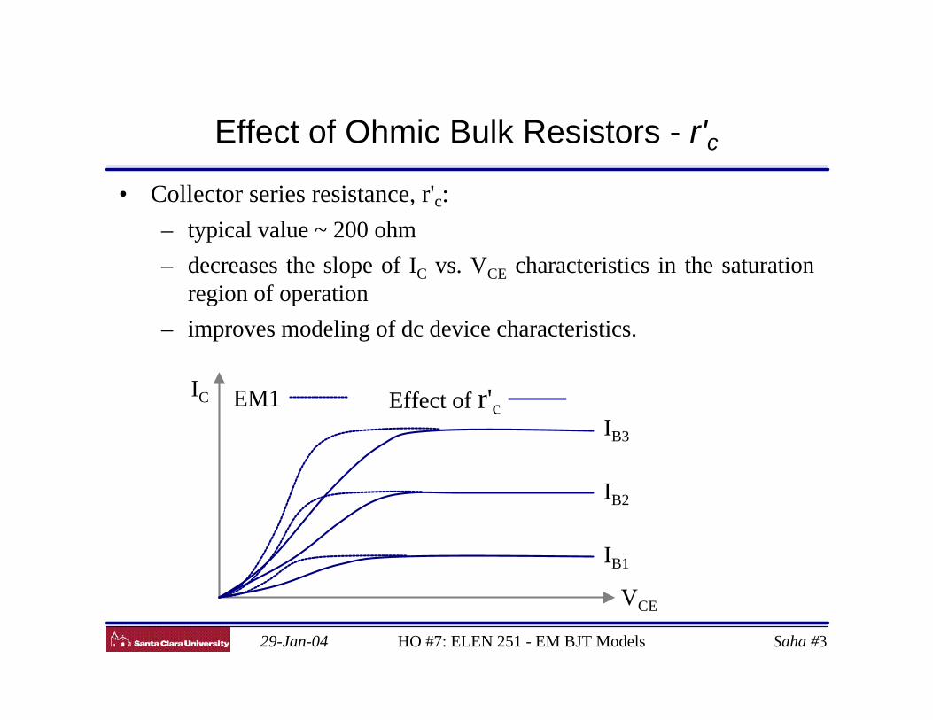
Effect of Ohmic Bulk Resistors - r'c
• Collector series resistance, r'c:– typical value ~ 200 ohm– decreases the slope of IC vs. VCE characteristics in the saturation
region of operation– improves modeling of dc device characteristics.
VCE
IC
IB3
IB2
IB1
EM1 Effect of r'c
29-Jan-04 HO #7: ELEN 251 - EM BJT Models Saha #4
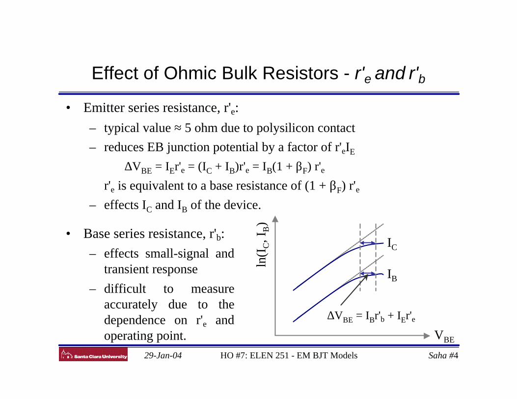
Effect of Ohmic Bulk Resistors - r'e and r'b
• Emitter series resistance, r'e:– typical value ≈ 5 ohm due to polysilicon contact– reduces EB junction potential by a factor of r'eIE
∆VBE = IEr'e = (IC + IB)r'e = IB(1 + βF) r'e∴ r'e is equivalent to a base resistance of (1 + βF) r'e– effects IC and IB of the device.
• Base series resistance, r'b:– effects small-signal and
transient response– difficult to measure
accurately due to thedependence on r'e andoperating point. VBE
ln(I
C, I
B)
IC
IB
∆VBE = IBr'b + IEr'e
29-Jan-04 HO #7: ELEN 251 - EM BJT Models Saha #5
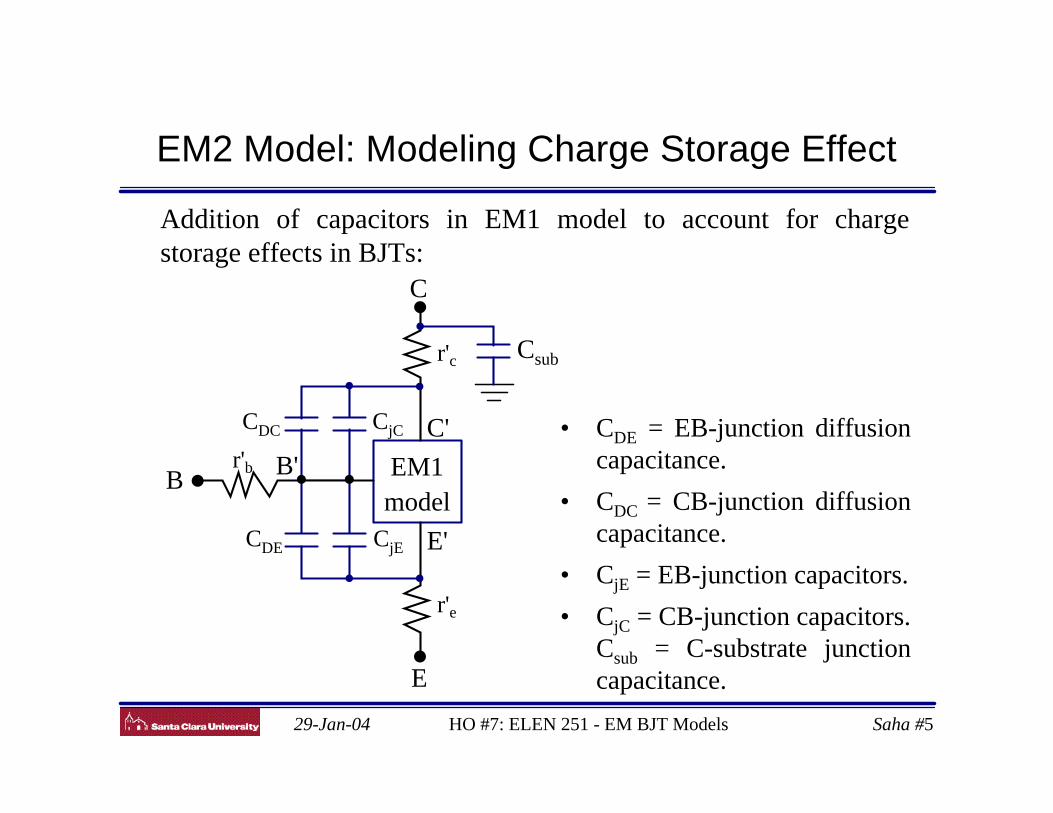
EM2 Model: Modeling Charge Storage Effect
Addition of capacitors in EM1 model to account for chargestorage effects in BJTs:
E
r'c
r'e
r'b EM1model
B
C
B'C'
E'
Csub
CjC
CjE
CDC
CDE
• CDE = EB-junction diffusioncapacitance.
• CDC = CB-junction diffusioncapacitance.
• CjE = EB-junction capacitors.
• CjC = CB-junction capacitors.Csub = C-substrate junctioncapacitance.
29-Jan-04 HO #7: ELEN 251 - EM BJT Models Saha #6
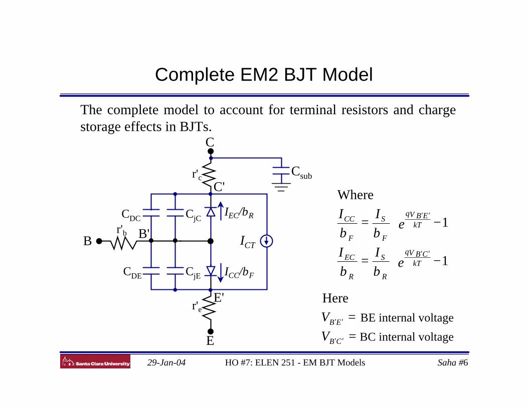
Complete EM2 BJT Model
The complete model to account for terminal resistors and chargestorage effects in BJTs.
E
r'c
r'e
r'bB
C
B'
C'
E'
Csub
CjC
CjE
CDC
CDE
ICT
IEC/βR
ICC/βF
−=
−=
′′
′′
1
1
Where
eII
eII
kTV CBq
R
S
R
EC
kTV EBq
F
S
F
CC
ββ
ββ
==
′′
′′
CB
EB
VVHere
BE internal voltage
BC internal voltage
29-Jan-04 HO #7: ELEN 251 - EM BJT Models Saha #7
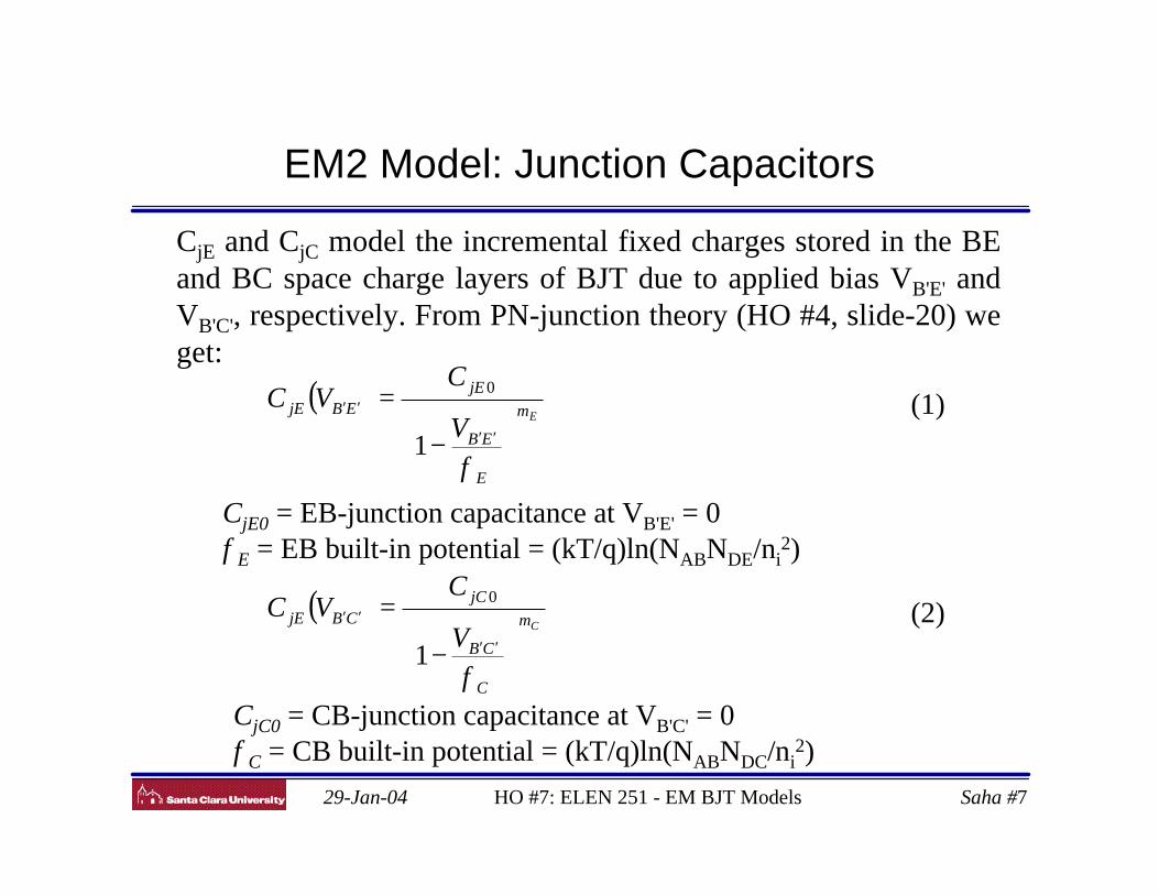
EM2 Model: Junction Capacitors
CjE and CjC model the incremental fixed charges stored in the BEand BC space charge layers of BJT due to applied bias VB'E' andVB'C', respectively. From PN-junction theory (HO #4, slide-20) weget:
( )Em
E
EB
jEEBjE
V
CVC
−
=′′
′′
φ1
0(1)
( )Cm
C
CB
jCCBjE
V
CVC
−
=′′
′′
φ1
0(2)
CjE0 = EB-junction capacitance at VB'E' = 0 φE = EB built-in potential = (kT/q)ln(NABNDE/ni
2)
CjC0 = CB-junction capacitance at VB'C' = 0 φC = CB built-in potential = (kT/q)ln(NABNDC/ni
2)
29-Jan-04 HO #7: ELEN 251 - EM BJT Models Saha #8
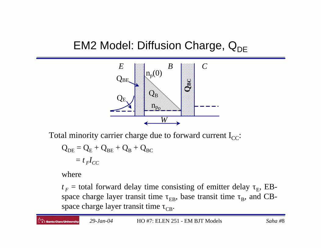
EM2 Model: Diffusion Charge, QDE
Total minority carrier charge due to forward current ICC: QDE = QE + QBE + QB + QBC
= τFICC
where
τF = total forward delay time consisting of emitter delay τE, EB-space charge layer transit time τEB, base transit time τB, and CB-space charge layer transit time τCB.
E Cnp(0)
npo
B
QBQE
QB
CQBE
W
29-Jan-04 HO #7: ELEN 251 - EM BJT Models Saha #9
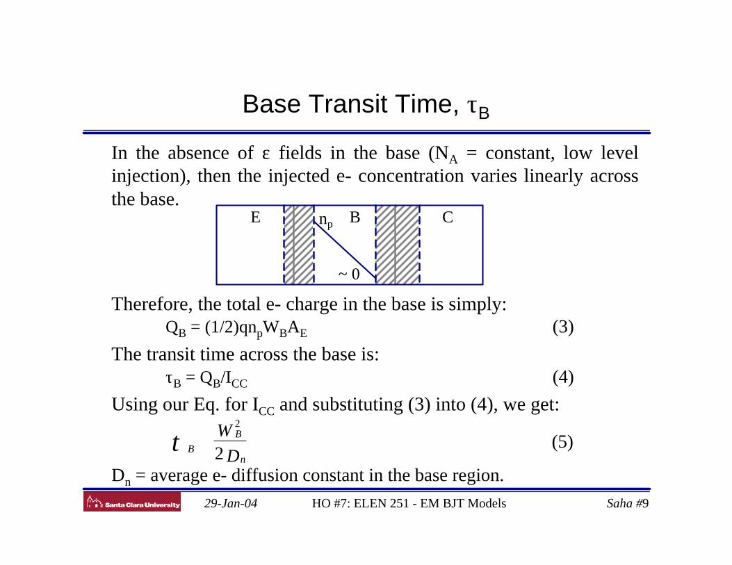
Base Transit Time, τB
In the absence of ε fields in the base (NA = constant, low levelinjection), then the injected e- concentration varies linearly acrossthe base.
Therefore, the total e- charge in the base is simply: QB = (1/2)qnpWBAE (3)
The transit time across the base is: τB = QB/ICC (4)
Using our Eq. for ICC and substituting (3) into (4), we get:
Dn = average e- diffusion constant in the base region.D
Wn
BB 2
2
≅τ (5)
npE B C
~ 0
29-Jan-04 HO #7: ELEN 251 - EM BJT Models Saha #10
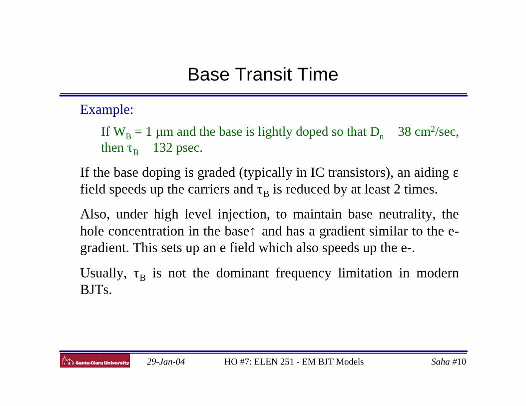
Base Transit Time
Example:
If WB = 1 µm and the base is lightly doped so that Dn ≅ 38 cm2/sec,then τB ≅ 132 psec.
If the base doping is graded (typically in IC transistors), an aiding εfield speeds up the carriers and τB is reduced by at least 2 times.
Also, under high level injection, to maintain base neutrality, thehole concentration in the base↑ and has a gradient similar to the e-gradient. This sets up an e field which also speeds up the e-.
Usually, τB is not the dominant frequency limitation in modernBJTs.
29-Jan-04 HO #7: ELEN 251 - EM BJT Models Saha #11
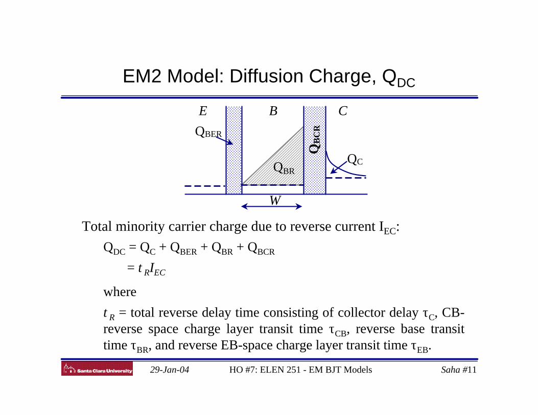
EM2 Model: Diffusion Charge, QDC
Total minority carrier charge due to reverse current IEC: QDC = QC + QBER + QBR + QBCR
= τRIEC
where
τR = total reverse delay time consisting of collector delay τC, CB-reverse space charge layer transit time τCB, reverse base transittime τBR, and reverse EB-space charge layer transit time τEB.
E CB
QBRQC
QB
CRQBER
W
29-Jan-04 HO #7: ELEN 251 - EM BJT Models Saha #12
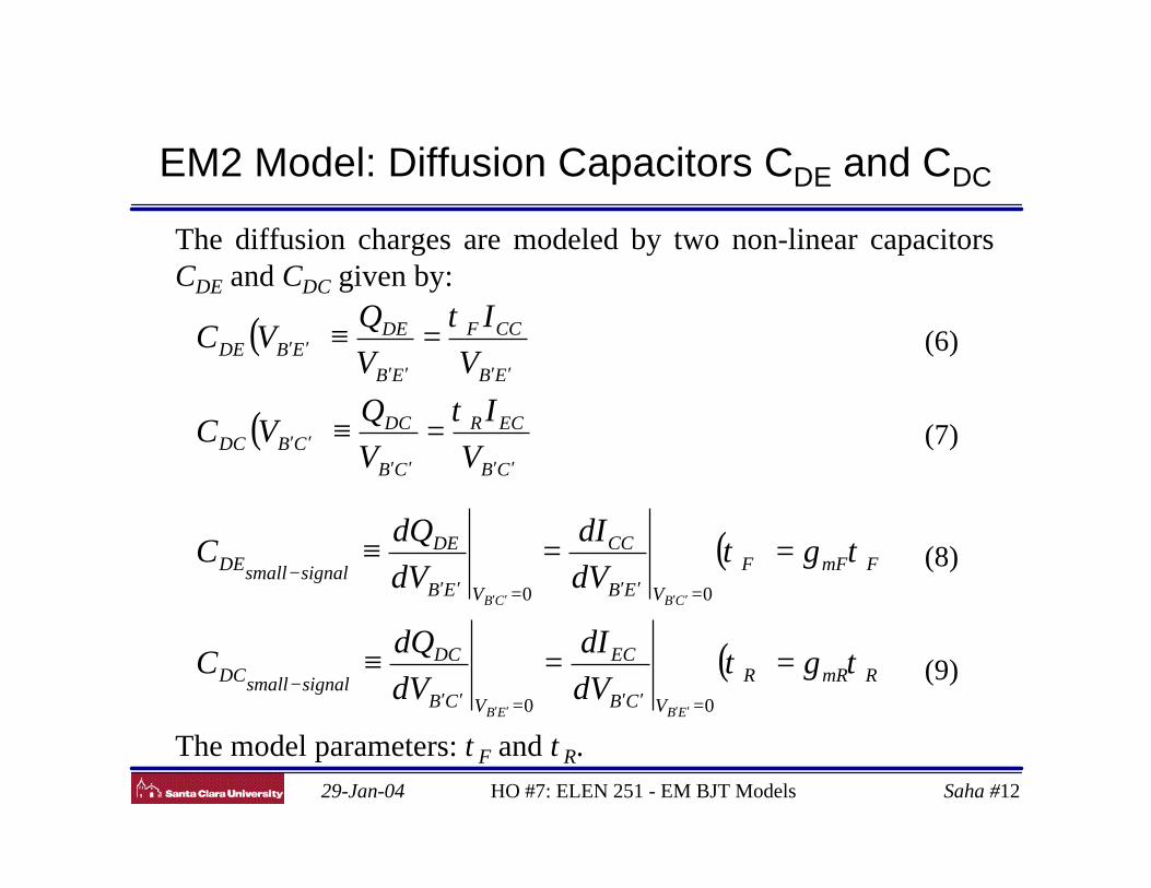
EM2 Model: Diffusion Capacitors CDE and CDC
The diffusion charges are modeled by two non-linear capacitorsCDE and CDC given by:
The model parameters: τF and τR.
( )
( )CB
ECR
CB
DCCBDC
EB
CCF
EB
DEEBDE
VI
VQ
VC
VI
VQ
VC
′′′′′′
′′′′′′
=≡
=≡
τ
τ(6)
(7)
( )
( ) RmRR
VCB
EC
VCB
DC
signalsmallDC
FmFF
VEB
CC
VEB
DE
signalsmallDE
gdVdI
dVdQ
C
gdVdI
dVdQ
C
EBEB
CBCB
ττ
ττ
==≡
==≡
=′′=′′−
=′′=′′−
′′′′
′′′′
00
00
(8)
(9)
29-Jan-04 HO #7: ELEN 251 - EM BJT Models Saha #13
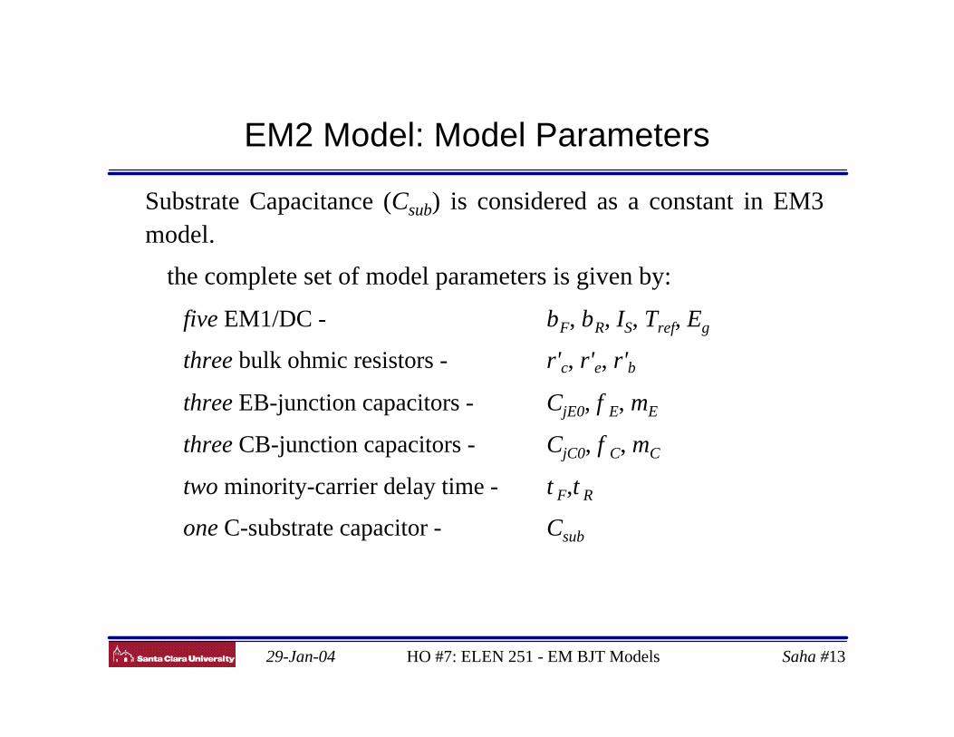
EM2 Model: Model Parameters
Substrate Capacitance (Csub) is considered as a constant in EM3model.
∴the complete set of model parameters is given by:
five EM1/DC - βF, βR, IS, Tref, Eg
three bulk ohmic resistors - r'c, r'e, r'b
three EB-junction capacitors - CjE0, φE, mE
three CB-junction capacitors - CjC0, φC, mC
two minority-carrier delay time - τF,τR
one C-substrate capacitor - Csub
29-Jan-04 HO #7: ELEN 251 - EM BJT Models Saha #14
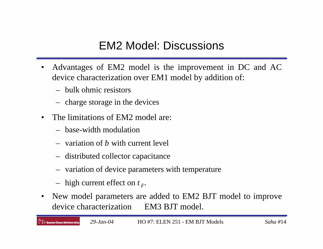
EM2 Model: Discussions
• Advantages of EM2 model is the improvement in DC and ACdevice characterization over EM1 model by addition of:– bulk ohmic resistors– charge storage in the devices
• The limitations of EM2 model are:– base-width modulation
– variation of β with current level
– distributed collector capacitance
– variation of device parameters with temperature
– high current effect on τF.
• New model parameters are added to EM2 BJT model to improvedevice characterization ⇒ EM3 BJT model.
29-Jan-04 HO #7: ELEN 251 - EM BJT Models Saha #15
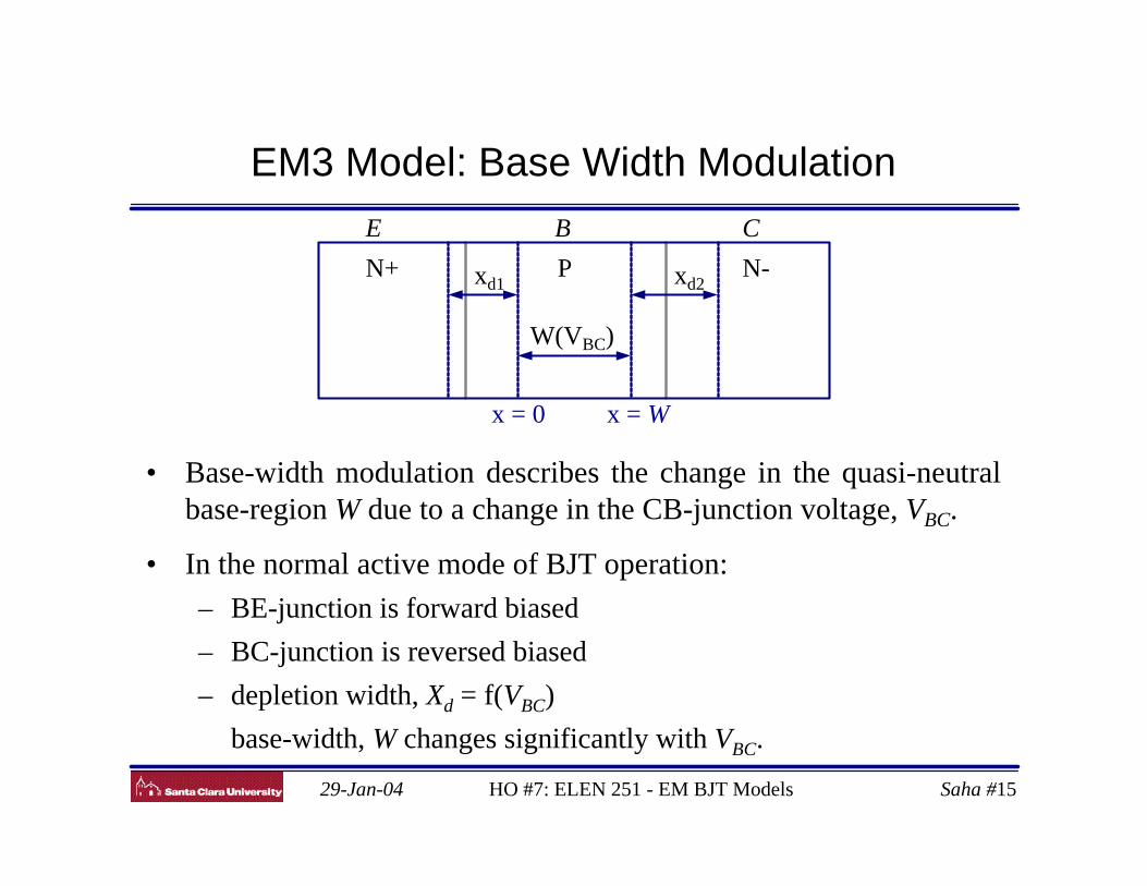
EM3 Model: Base Width Modulation
• Base-width modulation describes the change in the quasi-neutralbase-region W due to a change in the CB-junction voltage, VBC.
• In the normal active mode of BJT operation:– BE-junction is forward biased– BC-junction is reversed biased– depletion width, Xd = f(VBC)∴ base-width, W changes significantly with VBC.
BE C
W(VBC)
N+ P N-xd2xd1
x = 0 x = W
29-Jan-04 HO #7: ELEN 251 - EM BJT Models Saha #16
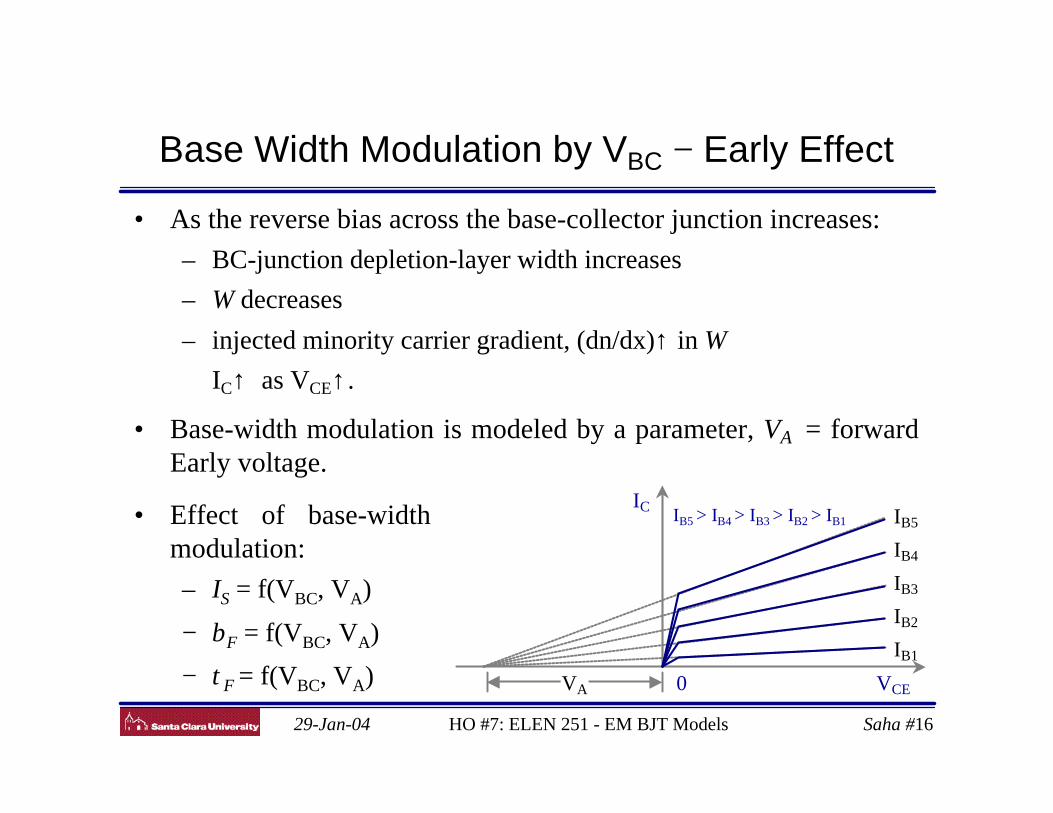
Base Width Modulation by VBC − Early Effect
• As the reverse bias across the base-collector junction increases:– BC-junction depletion-layer width increases– W decreases
– injected minority carrier gradient, (dn/dx)↑ in W∴ IC↑ as VCE↑.
• Base-width modulation is modeled by a parameter, VA = forwardEarly voltage.
IB5
IB4
IB3
IB2
IB1
VA VCE
IC IB5 > IB4 > IB3 > IB2 > IB1
0
• Effect of base-widthmodulation:– IS = f(VBC, VA)
− βF = f(VBC, VA)
− τF = f(VBC, VA)
29-Jan-04 HO #7: ELEN 251 - EM BJT Models Saha #17
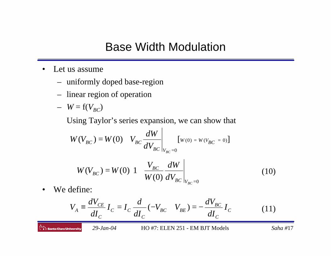
Base Width Modulation
• Let us assume– uniformly doped base-region– linear region of operation– W = f(VBC)
∴ Using Taylor’s series expansion, we can show that
• We define:
+=∴
+=
=
==
=
0
)0()0(
0
)0(1)0()(
][)0()(
BC
BC
VBC
BCBC
BCVWW
VBCBCBC
dVdW
WV
WVW
dVdW
VWVW
(10)
CC
BCBEBC
CCC
C
CEA I
dIdV
VVdId
IIdI
dVV −=+−=≡ )( (11)
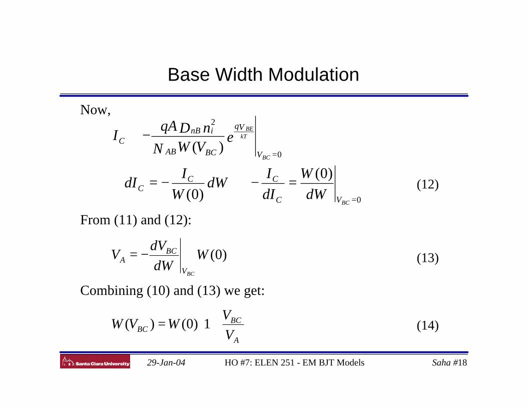
29-Jan-04 HO #7: ELEN 251 - EM BJT Models Saha #18
Base Width Modulation
Now,
From (11) and (12):
Combining (10) and (13) we get:
)0(WdW
dVV
BCV
BCA −= (13)
(12)0
0
2
)0()0(
)(
=
=
=−⇒−=∴
−≅
BC
BC
kTBE
VC
CCC
V
Vq
BCAB
inBC
dWW
dII
dWW
IdI
eVWNnDqA
I
+=
A
BCBC V
VWVW 1)0()( (14)
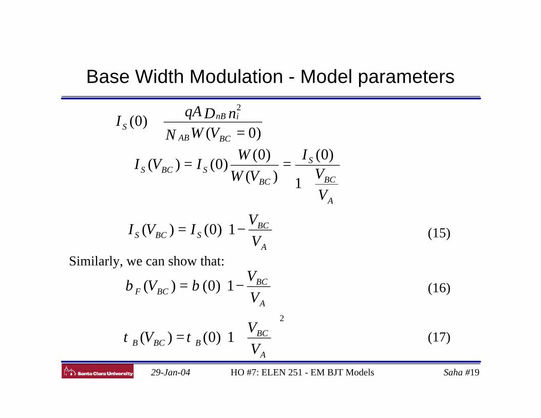
29-Jan-04 HO #7: ELEN 251 - EM BJT Models Saha #19
Base Width Modulation - Model parameters
(15)
−=∴
+==⇒
=≅
A
BCSBCS
A
BC
S
BCSBCS
BCAB
inBS
VV
IVI
VV
IVW
WIVI
VWNnDqA
I
1)0()(
1
)0()(
)0()0()(
)0()0(
2
Similarly, we can show that:
2
1)0()(
1)0()(
+=
−=
A
BCBBCB
A
BCBCF
VV
V
VV
V
ττ
ββ (16)
(17)
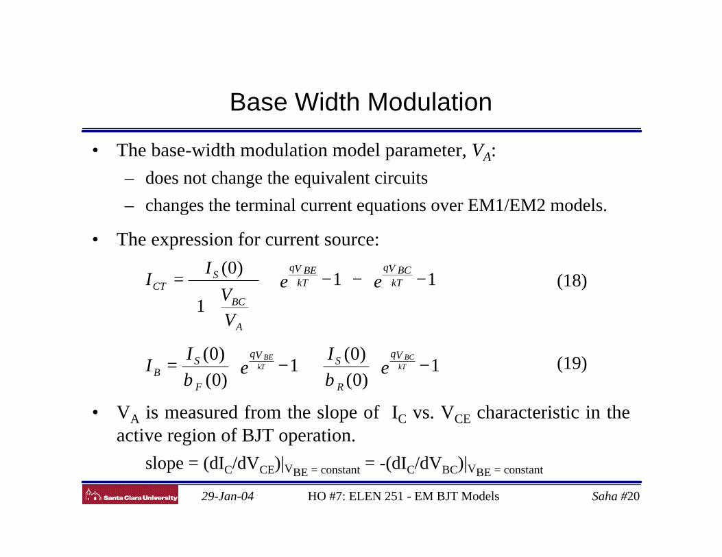
29-Jan-04 HO #7: ELEN 251 - EM BJT Models Saha #20
Base Width Modulation
• The base-width modulation model parameter, VA:– does not change the equivalent circuits– changes the terminal current equations over EM1/EM2 models.
• The expression for current source:
• VA is measured from the slope of IC vs. VCE characteristic in theactive region of BJT operation. slope = (dIC/dVCE)|VBE = constant = -(dIC/dVBC)|VBE = constant
−−
−
+
= 111
)0(ee
VV
II kT
V BCqkT
V BEq
A
BC
SCT (18)
−+
−= 1
)0()0(
1)0()0(
eI
eI
I kTBC
kTBE Vq
R
SVq
F
SB ββ
(19)
29-Jan-04 HO #7: ELEN 251 - EM BJT Models Saha #21
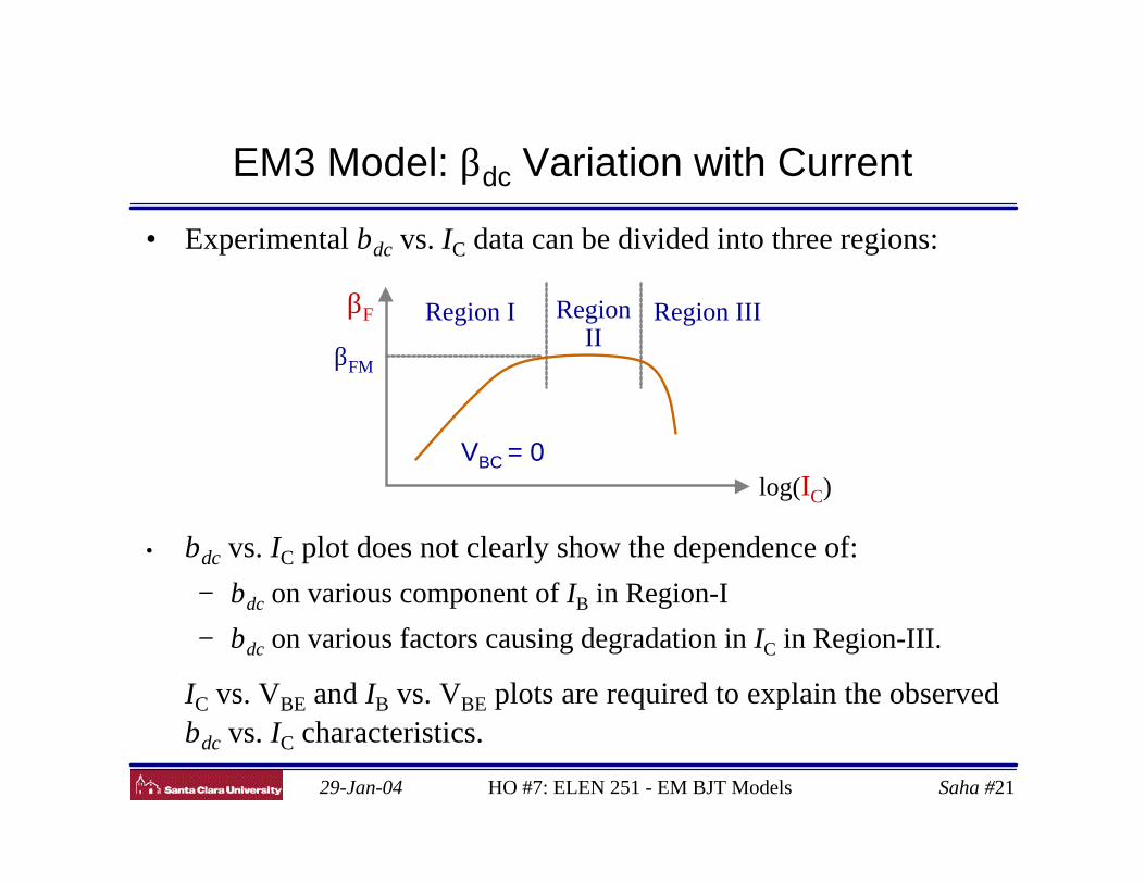
EM3 Model: βdc Variation with Current
• Experimental βdc vs. IC data can be divided into three regions:
Region I RegionII
Region III
log(IC)
βF
βFM
VBC = 0
• βdc vs. IC plot does not clearly show the dependence of:− βdc on various component of IB in Region-I
− βdc on various factors causing degradation in IC in Region-III.
∴ IC vs. VBE and IB vs. VBE plots are required to explain the observedβdc vs. IC characteristics.
29-Jan-04 HO #7: ELEN 251 - EM BJT Models Saha #22
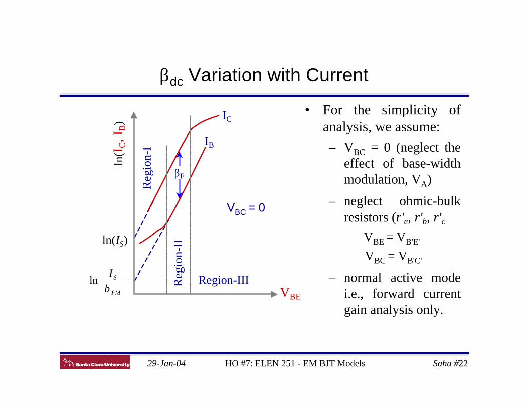
βdc Variation with Current
• For the simplicity ofanalysis, we assume:– VBC = 0 (neglect the
effect of base-widthmodulation, VA)
– neglect ohmic-bulkresistors (r'e, r'b, r'c)
⇒ VBE = VB'E'
VBC = VB'C'
– normal active modei.e., forward currentgain analysis only.
ln(I
C, I
B)
VBE
IB
IC
βF
Reg
ion-
I
Reg
ion-
II
Region-III
VBC = 0
ln(IS)
FM
SIβ
ln
29-Jan-04 HO #7: ELEN 251 - EM BJT Models Saha #23
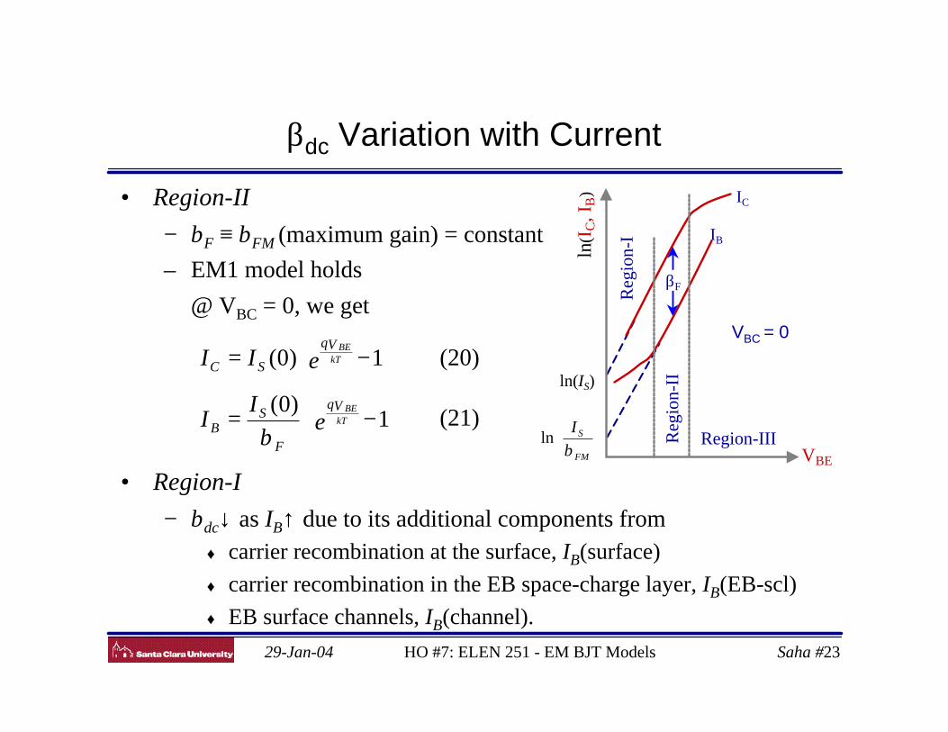
βdc Variation with Current
• Region-II− βF ≡ βFM (maximum gain) = constant– EM1 model holds∴ @ VBC = 0, we get
• Region-I− βdc↓ as IB↑ due to its additional components from
♦ carrier recombination at the surface, IB(surface)♦ carrier recombination in the EB space-charge layer, IB(EB-scl)♦ EB surface channels, IB(channel).
ln(I
C, I
B)
VBE
IB
IC
βFReg
ion-
I
Reg
ion-
II
Region-III
VBC = 0
ln(IS)
FM
SIβ
ln
−=
−=
1)0(
1)0(
eI
I
eII
kTBE
kTBE
Vq
F
SB
Vq
SC
β
(20)
(21)
29-Jan-04 HO #7: ELEN 251 - EM BJT Models Saha #24
βdc Variation with Current: Low IC Region
• ∆ΙB in (22) can be represented by an additional non-ideal EB-diode in the basic EM1 model with diode current given by:
• Here we have two new parameters for modeling low IC region:– nE = low-current forward emission coefficient (~ 2)– C2 = models various components of IS in low IB (~ 103).
−=∆∴
+−+≡∆
1)0()total(
)channel()sclEB()surface()total(Thus,
2 eICI
IIII
kTEBE
nVq
SB
BBBB
−1)0(2 eIC kTE
BEnVq
S
(22)
−+
−=∴ 1)0(1
)0(2 eICe
II kTE
BEkT
BEnVq
S
Vq
FM
SB β
(23)
29-Jan-04 HO #7: ELEN 251 - EM BJT Models Saha #25
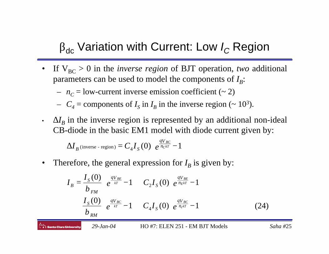
βdc Variation with Current: Low IC Region
• If VBC > 0 in the inverse region of BJT operation, two additionalparameters can be used to model the components of IB:– nC = low-current inverse emission coefficient (~ 2)– C4 = components of IS in IB in the inverse region (~ 103).
• ∆ΙB in the inverse region is represented by an additional non-idealCB-diode in the basic EM1 model with diode current given by:
• Therefore, the general expression for IB is given by:
−=∆ 1)0(4)region-inverse( eICI kTC
BCnVq
SB
−+
−+
−+
−=
1)0(1)0(
1)0(1)0(
4
2
eICeI
eICeI
I
kTcBC
kTBC
kTEBE
kTBE
nVq
S
Vq
RM
S
nVq
S
Vq
FM
SB
β
β
(24)
29-Jan-04 HO #7: ELEN 251 - EM BJT Models Saha #26
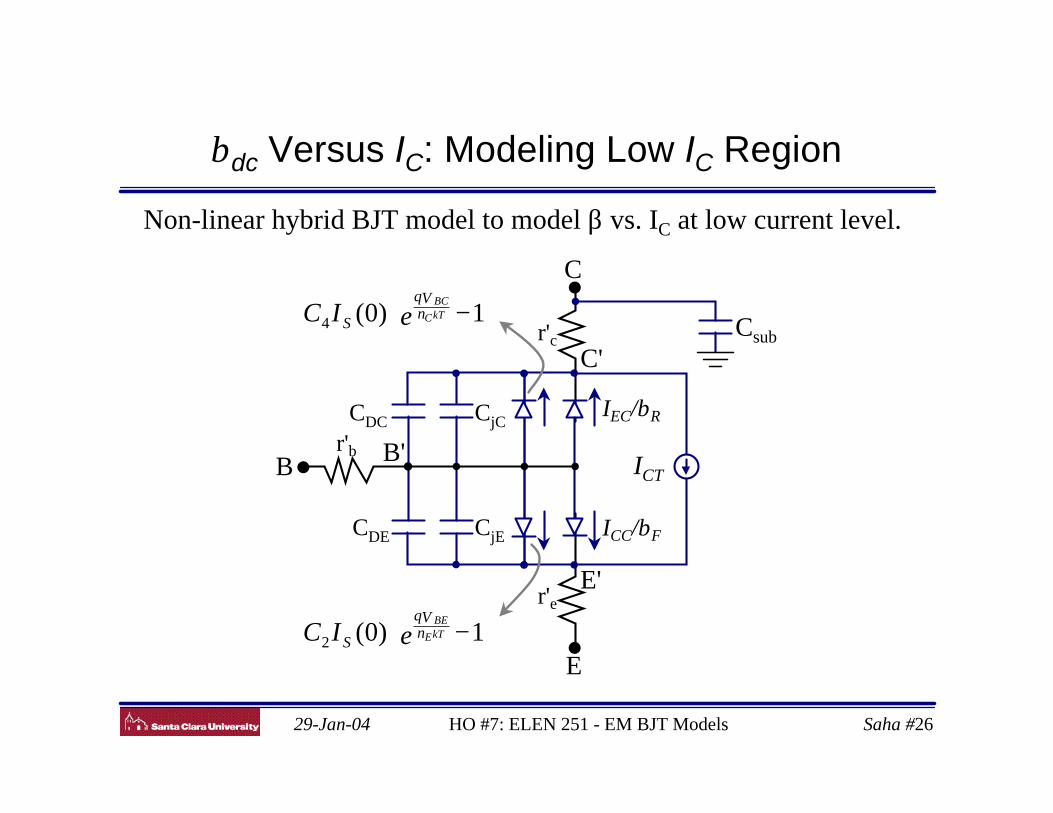
βdc Versus IC: Modeling Low IC Region
E
r'c
r'e
C
C'
E'
Csub
r'bB B'
CjC
CjE
CDC
CDE
ICT
IEC/βR
ICC/βF
−1)0(2 eIC kTE
BEnVq
S
−1)0(4 eIC kTC
BCnVq
S
Non-linear hybrid BJT model to model β vs. IC at low current level.
29-Jan-04 HO #7: ELEN 251 - EM BJT Models Saha #27
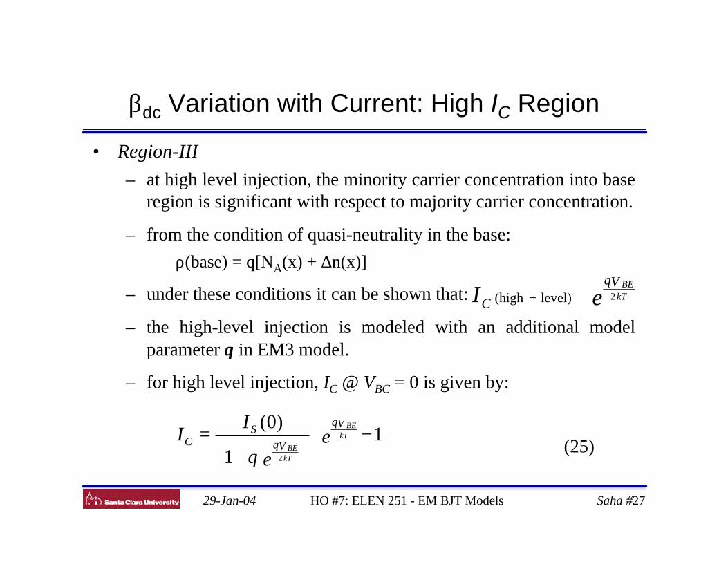
βdc Variation with Current: High IC Region
• Region-III– at high level injection, the minority carrier concentration into base
region is significant with respect to majority carrier concentration.
– from the condition of quasi-neutrality in the base: ρ(base) = q[NA(x) + ∆n(x)]
– under these conditions it can be shown that:
– the high-level injection is modeled with an additional modelparameter θ in EM3 model.
– for high level injection, IC @ VBC = 0 is given by:
eI kTBEVq
C2level)(high ∝−
−
+
= 11
)0(
2
ee
II kT
BE
kTBE
Vq
VqS
C
θ (25)
29-Jan-04 HO #7: ELEN 251 - EM BJT Models Saha #28
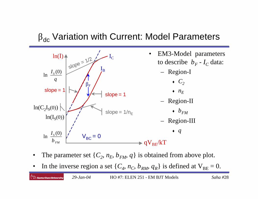
βdc Variation with Current: Model Parameters
ln(I)
qVBE/kT
IB
IC
βF
VBC = 0
ln(IS(0))
FM
SIβ
)0(ln
ln(C2IS(0))
θ)0(
ln SI
slope = 1slope = 1
slope = 1/nE
slope = 1/2• EM3-Model parameters
to describe βF - IC data:– Region-I
♦ C2
♦ nE
– Region-II♦ βFM
– Region-III♦ θ
• The parameter set {C2, nE, βFM, θ} is obtained from above plot.
• In the inverse region a set {C4, nC, βRM, θR} is defined at VBE = 0.
29-Jan-04 HO #7: ELEN 251 - EM BJT Models Saha #29
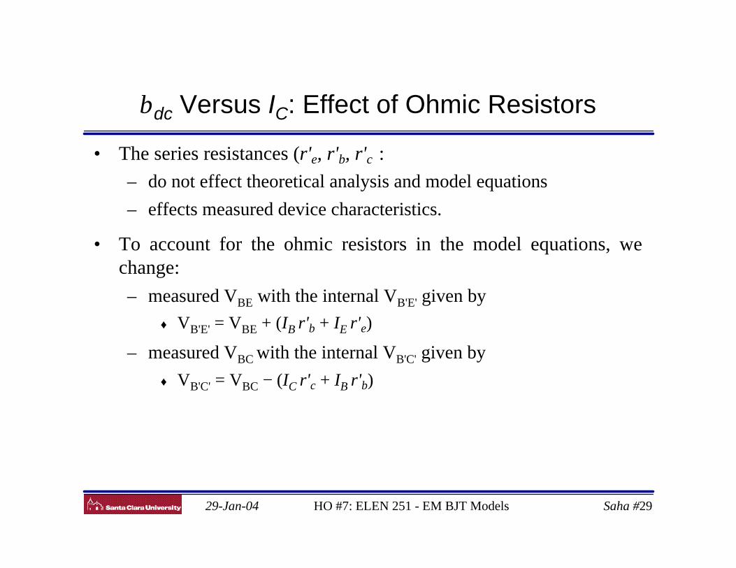
βdc Versus IC: Effect of Ohmic Resistors
• The series resistances (r'e, r'b, r'c):– do not effect theoretical analysis and model equations– effects measured device characteristics.
• To account for the ohmic resistors in the model equations, wechange:– measured VBE with the internal VB'E' given by
♦ VB'E' = VBE + (IB r'b + IE r'e)
– measured VBC with the internal VB'C' given by♦ VB'C' = VBC − (IC r'c + IB r'b)
29-Jan-04 HO #7: ELEN 251 - EM BJT Models Saha #30
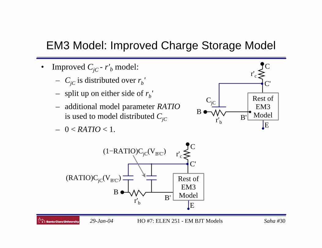
EM3 Model: Improved Charge Storage Model
• Improved CjC - r'b model:
– CjC is distributed over rb'
– split up on either side of rb'
– additional model parameter RATIOis used to model distributed CjC
– 0 < RATIO < 1. E
r'cC
C'
r'bB
B'
CjCRest ofEM3
Model
E
r'cC
C'
r'bB
B'
(RATIO)CjC(VB'C') Rest ofEM3
Model
(1−RATIO)CjC(VB'C')
29-Jan-04 HO #7: ELEN 251 - EM BJT Models Saha #31
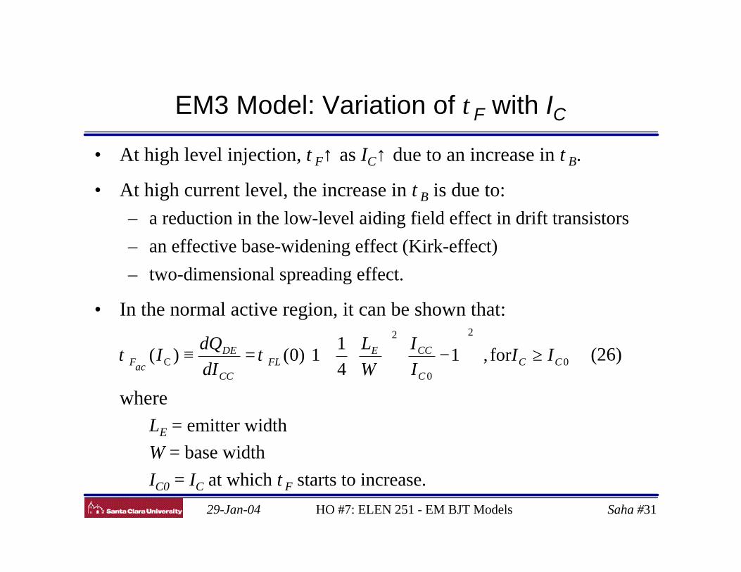
EM3 Model: Variation of τF with IC
• At high level injection, τF↑ as IC↑ due to an increase in τB.
• At high current level, the increase in τB is due to:– a reduction in the low-level aiding field effect in drift transistors– an effective base-widening effect (Kirk-effect)– two-dimensional spreading effect.
• In the normal active region, it can be shown that:
where LE = emitter width W = base width IC0 = IC at which τF starts to increase.
0
2
0
2
C for,141
1)0()( CCC
CCEFL
CC
DE
acF IIII
WL
dIdQ
I ≥
−
+=≡ ττ (26)
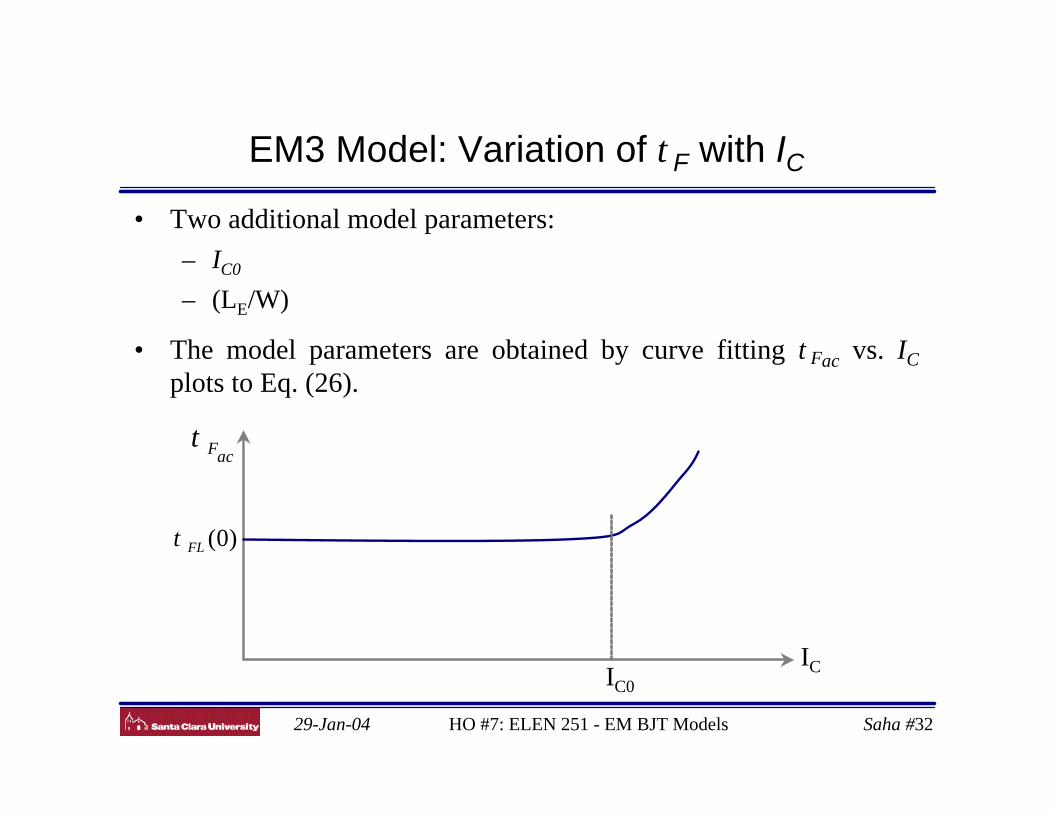
29-Jan-04 HO #7: ELEN 251 - EM BJT Models Saha #32
EM3 Model: Variation of τF with IC
• Two additional model parameters:– IC0
– (LE/W)
• The model parameters are obtained by curve fitting τFac vs. ICplots to Eq. (26).
ICIC0
acFτ
)0(FLτ
29-Jan-04 HO #7: ELEN 251 - EM BJT Models Saha #33
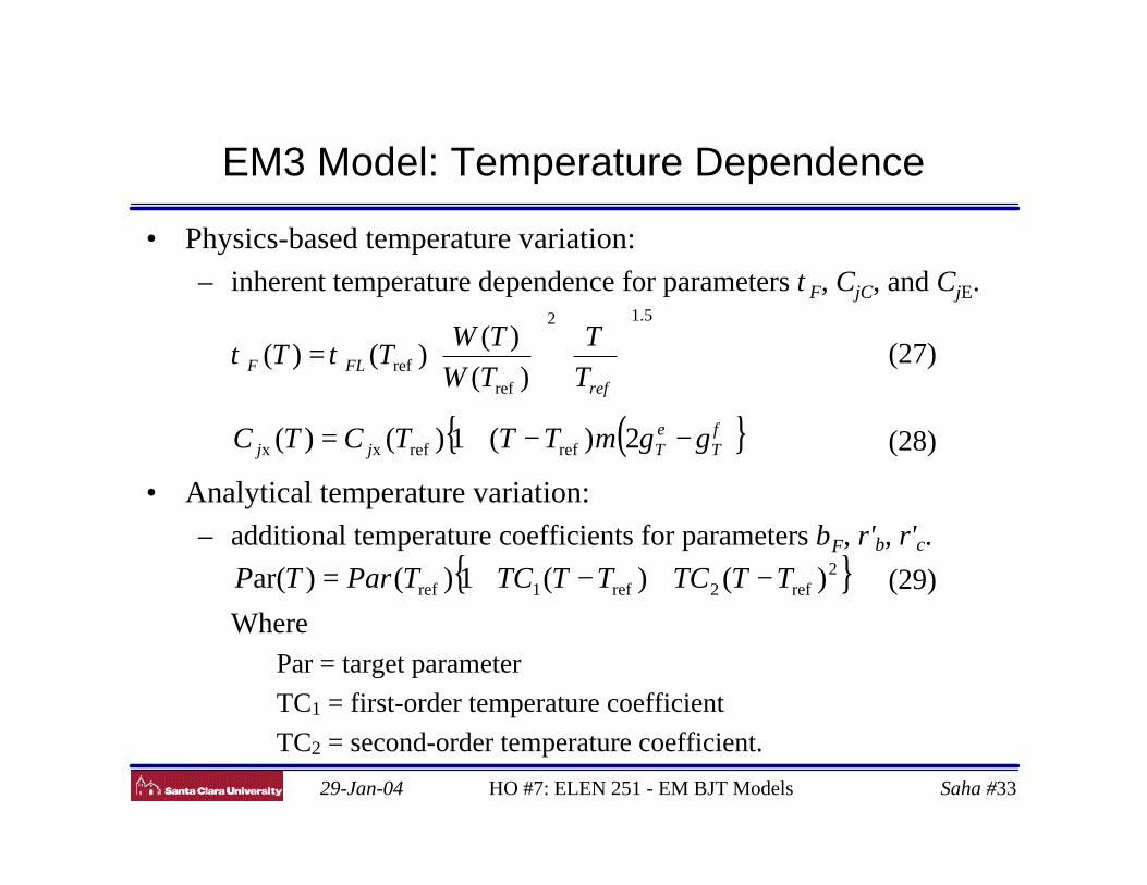
EM3 Model: Temperature Dependence
• Physics-based temperature variation:– inherent temperature dependence for parameters τF, CjC, and CjE.
• Analytical temperature variation:– additional temperature coefficients for parameters βF, r'b, r'c.
Where Par = target parameter TC1 = first-order temperature coefficient TC2 = second-order temperature coefficient.
5.12
refref )(
)()()(
=
refFLF T
TTWTW
TT ττ (27)
( ){ }φε γγ TTjj mTTTCTC −−+= 2)(1)()( refrefxx (28)
{ }2ref2ref1ref )()(1)()ar( TTTCTTTCTParTP −+−+= (29)
29-Jan-04 HO #7: ELEN 251 - EM BJT Models Saha #34
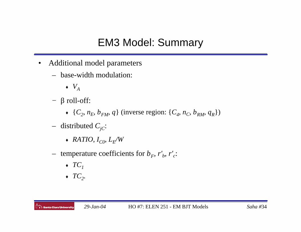
EM3 Model: Summary
• Additional model parameters– base-width modulation:
♦ VA
− β roll-off:♦ {C2, nE, βFM, θ} (inverse region: {C4, nC, βRM, θR})
– distributed CjC:
♦ RATIO, IC0, LE/W
– temperature coefficients for βF, r'b, r'c:♦ TC1
♦ TC2.