Lecture 19 Bipolar Junction Transistors (BJT): Part 3...
13
ECE 3040 - Dr. Alan Doolittle Georgia Tech Lecture 19 Bipolar Junction Transistors (BJT): Part 3 Ebers Moll Large Signal BJT Model, Using CVD model to solve for DC bias point Reading: Pierret 11.1
Transcript of Lecture 19 Bipolar Junction Transistors (BJT): Part 3...

ECE 3040 - Dr. Alan Doolittle Georgia Tech
Lecture 19
Bipolar Junction Transistors (BJT): Part 3
Ebers Moll Large Signal BJT Model, Using CVD model to solve for DC bias point
Reading:
Pierret 11.1
ECE 3040 - Dr. Alan Doolittle Georgia Tech
IE IC
IB
Collector
Base
Emitter
αFIF
IF
−= 10
TEB
VV
FF eII
DiodesIdeal
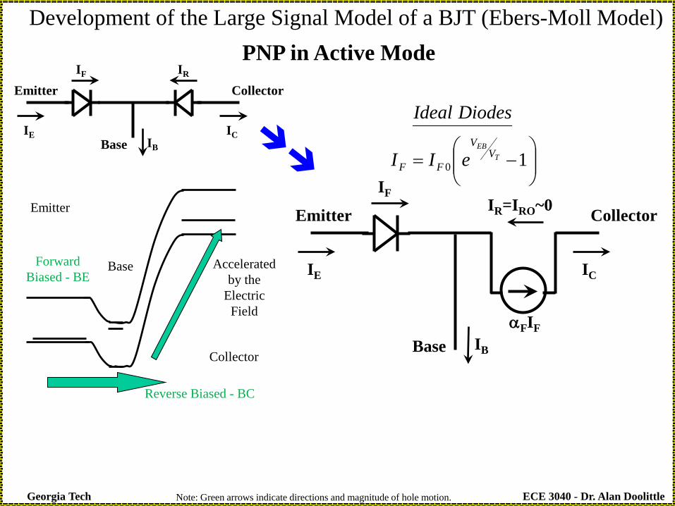
Development of the Large Signal Model of a BJT (Ebers-Moll Model) PNP in Active Mode
Emitter
Base
Collector
Forward Biased - BE
Reverse Biased - BC
Accelerated by the
Electric Field
IR=IRO~0
IE IC IB
Collector
Base
Emitter IF IR
Note: Green arrows indicate directions and magnitude of hole motion.
ECE 3040 - Dr. Alan Doolittle Georgia Tech
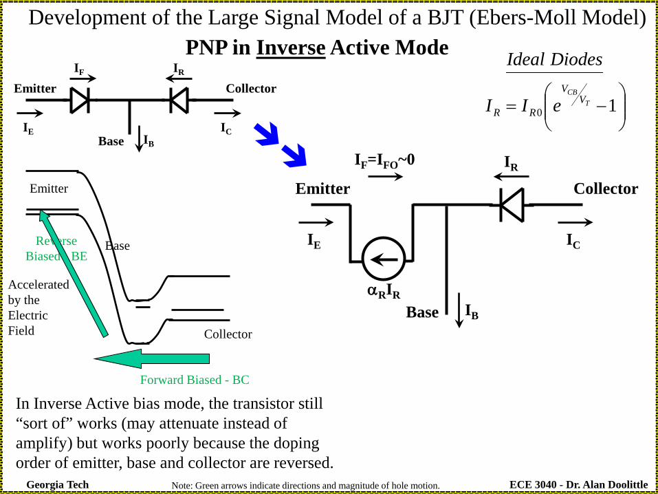
Development of the Large Signal Model of a BJT (Ebers-Moll Model) PNP in Inverse Active Mode
Emitter
Base
Collector
Reverse Biased - BE
Forward Biased - BC
Accelerated by the Electric Field
In Inverse Active bias mode, the transistor still “sort of” works (may attenuate instead of amplify) but works poorly because the doping order of emitter, base and collector are reversed.
IE IC
IB
Collector
Base
Emitter
αRIR
IF=IFO~0 IR
−= 10
TCB
VV
RR eII
DiodesIdeal
IE IC IB
Collector
Base
Emitter IF IR
Note: Green arrows indicate directions and magnitude of hole motion.
ECE 3040 - Dr. Alan Doolittle Georgia Tech
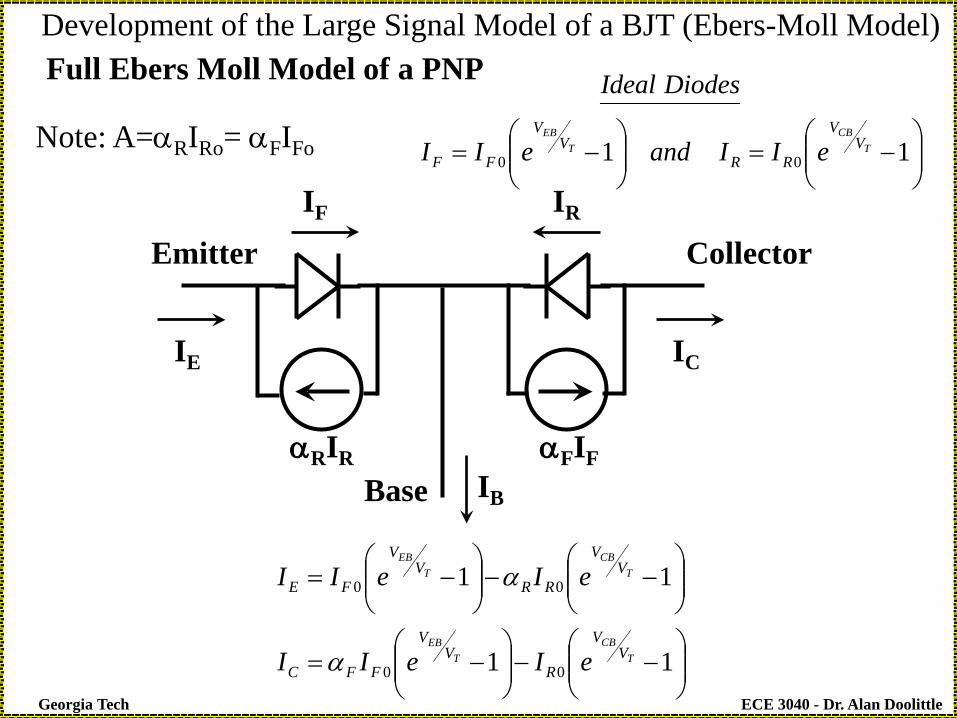
Note: A=αRIRo= αFIFo
IE IC
IB
Collector
Base
Emitter
αFIF αRIR
IF IR
−=
−= 11 00
TCB
TEB
VV
RRV
V
FF eIIandeII
DiodesIdeal
−−
−=
−−
−=
11
11
00
00
TCB
TEB
TCB
TEB
VV
RV
V
FFC
VV
RRV
V
FE
eIeII
eIeII
α
α
Development of the Large Signal Model of a BJT (Ebers-Moll Model) Full Ebers Moll Model of a PNP
ECE 3040 - Dr. Alan Doolittle Georgia Tech
Development of the Large Signal Model of a BJT (Ebers-Moll Model)
IE IC
IB
Collector
Base
Emitter
αFIF αRIR
IF IR
−=
−= 11 00
TBC
TBE
VV
RRV
V
FF eIIandeII
DiodesIdeal
−−
−=
−−
−=
11
11
00
00
TBC
TBE
TBC
TBB
VV
RV
V
FFC
VV
RRV
V
FE
eIeII
eIeII
α
α
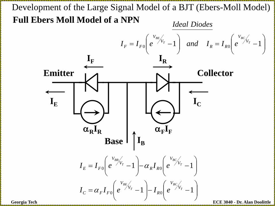
Full Ebers Moll Model of a NPN

ECE 3040 - Dr. Alan Doolittle Georgia Tech
Using the Ebers-Moll model requires mathematical complexity (and much pain). Thus, we have an approximate solution
method* that allows a quick solution.
*I refer to as the “CVD/Beta Analysis”. This is just my term, not a universal name.
ECE 3040 - Dr. Alan Doolittle Georgia Tech
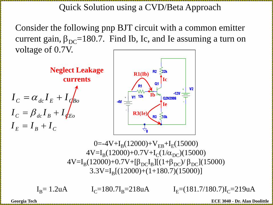
Quick Solution using a CVD/Beta Approach
Consider the following pnp BJT circuit with a common emitter current gain, βDC=180.7. Find Ib, Ic, and Ie assuming a turn on voltage of 0.7V.
0=-4V+IB(12000)+VEB+IE(15000) 4V=IB(12000)+0.7V+IC(1/αDC)(15000)
4V=IB(12000)+0.7V+[βDCIB][(1+βDC)/ βDC](15000) 3.3V=IB[(12000)+(1+180.7)(15000)]
IB= 1.2uA IC=180.7IB=218uA IE=(181.7/180.7)IC=219uA
CBoEdcC III +=α
CEoBdcC III += β
Neglect Leakage currents
R1(Ib)
R3(Ie)
Ie
Ib
Ic
CBE III +=
ECE 3040 - Dr. Alan Doolittle Georgia Tech
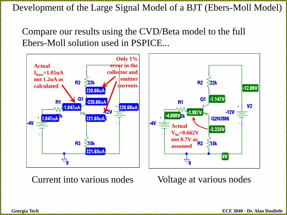
Development of the Large Signal Model of a BJT (Ebers-Moll Model)
Compare our results using the CVD/Beta model to the full Ebers-Moll solution used in PSPICE...
Actual Vbe=0.662V not 0.7V as assumed
Actual Ibase=1.05uA not 1.2uA as calculated
Only 1% error in the
collector and emitter
currents
Current into various nodes Voltage at various nodes
ECE 3040 - Dr. Alan Doolittle Georgia Tech
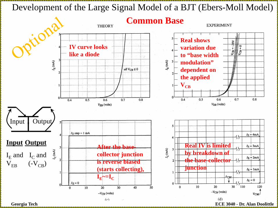
IV curve looks like a diode
Real shows variation due to “base width modulation” dependent on the applied VCB
After the base-collector junction is reverse biased (starts collecting), IE~=IC
Real IV is limited by breakdown of the base-collector junction
Development of the Large Signal Model of a BJT (Ebers-Moll Model) Common Base
Input
IE and VEB
Output
IC and (-VCB)
Input Output
ECE 3040 - Dr. Alan Doolittle Georgia Tech
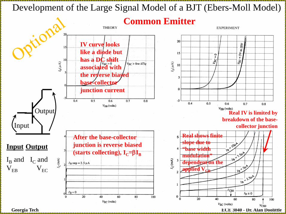
IV curve looks like a diode but has a DC shift associated with the reverse biased base-collector junction current
After the base-collector junction is reverse biased (starts collecting), IC=βIB
Development of the Large Signal Model of a BJT (Ebers-Moll Model)
Input
IB and VEB
Output
IC and VEC
Real IV is limited by breakdown of the base-
collector junction
Real shows finite slope due to “base width modulation” dependent on the applied VCB
Input
Output
Common Emitter
ECE 3040 - Dr. Alan Doolittle Georgia Tech
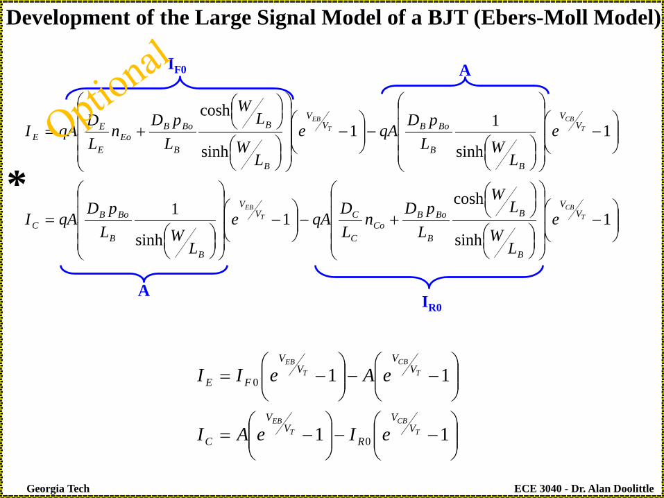
−−
−=
−−
−=
11
11
0
0
TCB
TEB
TCB
TEB
VV
RV
V
C
VV
VV
FE
eIeAI
eAeII
−
+−
−
=
−
−
−
+=
1sinh
cosh1
sinh
1
1sinh
11sinh
cosh
TCB
TEB
TCB
TEB
VV
B
B
B
BoBCo
C
CVV
B
B
BoBC
VV
B
B
BoBVV
B
B
B
BoBEo
E
EE
e
LW
LW
LpD
nLD
qAe
LWL
pDqAI
e
LWL
pDqAe
LW
LW
LpD
nLDqAI
IF0
IR0
A
A
*
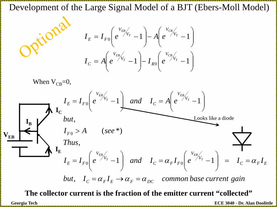
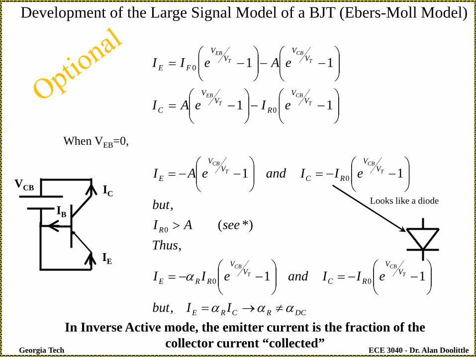
Development of the Large Signal Model of a BJT (Ebers-Moll Model)
ECE 3040 - Dr. Alan Doolittle Georgia Tech
−−
−=
−−
−=
11
11
0
0
TCB
TEB
TCB
TEB
VV
RV
V
C
VV
VV
FE
eIeAI
eAeII
When VCB=0,
gaincurrentbasecommonIIbut
IIeIIandeII
ThusseeAI
but
eAIandeII
DCFEFC
EFCV
V
FFCV
V
FE
F
VV
CV
V
FE
TEB
TEB
TEB
TEB
ααα
αα
=→=
==
−=
−=
>
−=
−=
,
11
,*)(
,
11
00
0
0
VEB
IB
IC
IE
Looks like a diode
Development of the Large Signal Model of a BJT (Ebers-Moll Model)
The collector current is the fraction of the emitter current “collected”
ECE 3040 - Dr. Alan Doolittle Georgia Tech
−−
−=
−−
−=
11
11
0
0
TCB
TEB
TCB
TEB
VV
RV
V
C
VV
VV
FE
eIeAI
eAeII
When VEB=0,
DCRCRE
VV
RCV
V
RRE
R
VV
RCV
V
E
IIbut
eIIandeII
ThusseeAI
but
eIIandeAI
TCB
TCB
TCB
TCB
ααα
α
≠→=
−−=
−−=
>
−−=
−−=
,
11
,*)(
,
11
00
0
0VCB
IB
IC
IE
Looks like a diode
In Inverse Active mode, the emitter current is the fraction of the collector current “collected”
Development of the Large Signal Model of a BJT (Ebers-Moll Model)