BIPOLAR ANALOG INTEGRATED CIRCUIT UPC2762TB · 2016-09-02 · 3 V, SUPER MINIMOLD BIPOLAR ANALOG...
7
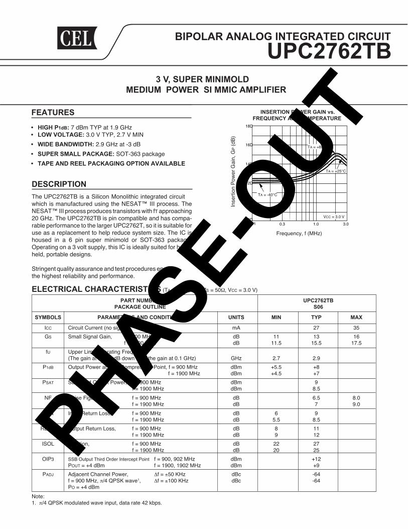
3 V, SUPER MINIMOLD BIPOLAR ANALOG INTEGRATED CIRCUIT MEDIUM POWER SI MMIC AMPLIFIER UPC2762TB INSERTION POWER GAIN vs. FREQUENCY AND TEMPERATURE Frequency, f (MHz) G , n i a G r e w o P n o i t r e s n I P ) B d ( Note: 1. π/4 QPSK modulated wave input, data rate 42 kbps. 0.1 0.3 1.0 3.0 VCC = 3.0 V TA = -40°C TA = +25°C TA = +85°C B T 2 6 7 2 C P U R E B M U N T R A P 6 0 S E N I L T U O E G A K C A P SYMBOLS PARAMETERS AND CONDITIONS UNITS MIN TYP MAX ICC 5 3 7 2 A m ) l a n g i s o n ( t n e r r u C t i u c r i C GS 6 1 3 1 1 1 B d z H M 0 0 9 = f , n i a G l a n g i S l l a m S 5 . 7 1 5 . 5 1 5 . 1 1 B d z H M 0 0 9 1 = f fU Upper Limit Operating Frequency (The gain at fu is 3 dB down from the gain at 0.1 GHz) GHz 2.7 2.9 P1dB Output Power at 1 dB Compression Point, f = 900 MHz dBm +5.5 +8 f = 1900 MHz dBm +4.5 +7 PSAT 9 m B d z H M 0 0 9 = f , r e w o P t u p t u O d e t a r u t a S 5 . 8 m B d z H M 0 0 9 1 = f 0 . 8 5 . 6 B d z H M 0 0 9 = f , e r u g i F e s i o N F N 0 . 9 7 B d z H M 0 0 9 1 = f RLIN 9 6 B d z H M 0 0 9 = f , s s o L n r u t e R t u p n I 5 . 8 5 . 5 B d z H M 0 0 9 1 = f RLOUT 1 1 8 B d z H M 0 0 9 = f , s s o L n r u t e R t u p t u O 2 1 9 B d z H M 0 0 9 1 = f 7 2 2 2 B d z H M 0 0 9 = f , n o i t a l o s I L O S I 5 2 0 2 B d z H M 0 0 9 1 = f OIP3 SSB Output Third Order Intercept Point 2 1 + m B d z H M 2 0 9 , 0 0 9 = f POUT 9 + m B d z H M 2 0 9 1 , 0 0 9 1 = f m B d 4 + = PADJ Adjacent Channel Power, Δf = ± 4 6 - c B d z H K 0 5 f = 900 MHz, π/4 QPSK wave 1 , Δf = ± 4 6 - c B d z H K 0 0 1 PO = +4 dBm ELECTRICAL CHARACTERISTICS (TA = 25°C, ZL = ZS = 50Ω, VCC = 3.0 V) The UPC2762TB is a Silicon Monolithic integrated circuit which is manufactured using the NESAT™ III process. The NESAT™ III process produces transistors with fT approaching 20 GHz. The UPC2762TB is pin compatible and has compa- rable performance to the larger UPC2762T, so it is suitable for use as a replacement to help reduce system size. The IC is housed in a 6 pin super minimold or SOT-363 package. Operating on a 3 volt supply, this IC is ideally suited for hand- held, portable designs. Stringent quality assurance and test procedures ensure the highest reliability and performance. • HIGH P1dB: 7 dBm TYP at 1.9 GHz • LOW VOLTAGE: 3.0 V TYP, 2.7 V MIN • WIDE BANDWIDTH: 2.9 GHz at -3 dB • SUPER SMALL PACKAGE: SOT-363 package • TAPE AND REEL PACKAGING OPTION AVAILABLE FEATURES DESCRIPTION PHASE-OUT
Transcript of BIPOLAR ANALOG INTEGRATED CIRCUIT UPC2762TB · 2016-09-02 · 3 V, SUPER MINIMOLD BIPOLAR ANALOG...
3 V, SUPER MINIMOLD
BIPOLAR ANALOG INTEGRATED CIRCUIT
MEDIUM POWER SI MMIC AMPLIFIER
UPC2762TB
INSERTION POWER GAIN vs.FREQUENCY AND TEMPERATURE
Frequency, f (MHz)G ,nia
G rewoP noitresnI
P)Bd(
Note:1. π/4 QPSK modulated wave input, data rate 42 kbps.
0.1 0.3 1.0 3.0
VCC = 3.0 V
TA = -40°C
TA = +25°C
TA = +85°C
BT2672CPUREBMUN TRAP60SENILTUO EGAKCAP
SYMBOLS PARAMETERS AND CONDITIONS UNITS MIN TYP MAX
ICC 5372Am)langis on( tnerruC tiucriCGS 613111BdzHM 009 = f,niaG langiS llamS
5.715.515.11BdzHM 0091 = ffU Upper Limit Operating Frequency
(The gain at fu is 3 dB down from the gain at 0.1 GHz) GHz 2.7 2.9P1dB Output Power at 1 dB Compression Point, f = 900 MHz dBm +5.5 +8
f = 1900 MHz dBm +4.5 +7PSAT 9mBdzHM 009 = f,rewoP tuptuO detarutaS
5.8mBdzHM 0091 = f0.85.6BdzHM 009 = f,erugiF esioNFN0.97BdzHM 0091 = f
RLIN 96BdzHM 009 = f,ssoL nruteR tupnI5.85.5BdzHM 0091 = f
RLOUT 118BdzHM 009 = f,ssoL nruteR tuptuO219BdzHM 0091 = f7222BdzHM 009 = f,noitalosILOSI5202BdzHM 0091 = f
OIP3 SSB Output Third Order Intercept Point 21+mBdzHM 209 ,009 = fPOUT 9+mBdzHM 2091 ,0091 = fmBd 4+ =
PADJ Adjacent Channel Power, Δf = ± 46-cBdzHK 05f = 900 MHz, π/4 QPSK wave1, Δf = ± 46-cBdzHK 001PO = +4 dBm
ELECTRICAL CHARACTERISTICS (TA = 25°C, ZL = ZS = 50Ω, VCC = 3.0 V)
The UPC2762TB is a Silicon Monolithic integrated circuitwhich is manufactured using the NESAT™ III process. TheNESAT™ III process produces transistors with fT approaching20 GHz. The UPC2762TB is pin compatible and has compa-rable performance to the larger UPC2762T, so it is suitable foruse as a replacement to help reduce system size. The IC ishoused in a 6 pin super minimold or SOT-363 package.Operating on a 3 volt supply, this IC is ideally suited for hand-held, portable designs.
Stringent quality assurance and test procedures ensurethe highest reliability and performance.
• HIGH P1dB: 7 dBm TYP at 1.9 GHz• LOW VOLTAGE: 3.0 V TYP, 2.7 V MIN• WIDE BANDWIDTH: 2.9 GHz at -3 dB• SUPER SMALL PACKAGE: SOT-363 package• TAPE AND REEL PACKAGING OPTION AVAILABLE
FEATURES
DESCRIPTION
PHASE-OUT
UPC2762TB
ABSOLUTE MAXIMUM RATINGS1 (TA = 25°C)
TEST CIRCUIT
Noi
se F
igur
e, N
F (
dB)
Frequency, f (GHz)
Supply Voltage, VCC (V)
Circ
uit C
urre
nt, I
CC (
mA
)
NOISE FIGURE ANDINSERTION POWER GAIN vs.FREQUENCY AND VOLTAGE
Circ
uit C
urre
nt, I
CC (
mA
)SYMBOLS PARAMETERS UNITS RATINGS
VCC Supply Voltage V 3.6
ICC Total Supply Current mA 70
PIN Input Power dBm +10
PT Total Power Dissipation2 mW 270TOP Operating Temperature °C -40 to +85
TSTG Storage Temperature °C -55 to +150
SYMBOLS PARAMETERS UNITS MIN TYP MAXVCC Supply Voltage V 2.7 3 3.3
TOP Operating Temperature °C -40 25 85
RECOMMENDED OPERATING CONDITIONS
Notes:1. Operation in excess of any one of these parameters may result
in permanent damage.2. Mounted on a 50 x 50 x 1.6 mm epoxy glass PWB (TA = 85°C).
INPUT AND OUTPUTRETURN LOSS vs.
FREQUENCY
Ret
urn
Loss
(dB
)
Gai
n, G
S (d
B)
Frequency, f (GHz)
Operating Temperature, TOP (°C)
CIRCUIT CURRENT vs.SUPPLY VOLTAGE
TYPICAL PERFORMANCE CURVES (TA = 25°C)
CIRCUIT CURRENT vs.OPERATING TEMPERATURE
VCC
50 ΩOUT
1000 pF
IN50 Ω
1000 pF
1000 pF
6
1 4
2, 3, 5
L = 300 nH
50
40
30
20
10
0
0 1 2 3 4
20
18
16
14
12
10
8
6
4
20.1 0.3 1.0 3.0
VCC = 3.3 VVCC = 3.0 V
VCC = 2.7 V
VCC = 2.7 VVCC = 3.0 V
VCC = 3.3 V
GS
NF
10
8
6
2
4
50
40
30
10
0
20
-60 -40 -20 0 20 40 60 80 100
No signalVCC = 3.0 V
0.1 0.3 1.0 3.0
0
-10
-20
-30
-40
VCC = 3.0V
RLin
RLoutPHASE-OUT
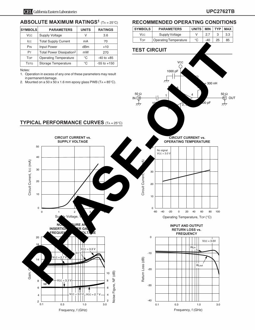
TYPICAL PERFORMANCE CURVES (TA = 25°C)
OUTPUT POWER vs.INPUT POWER AND VOLTAGE
Input Power, PIN (dBm)Frequency, f (GHz)
Isol
atio
n, IS
OL
(dB
)
OUTPUT POWER vs.INPUT POWER AND VOLTAGE
Out
put P
ower
, PO
UT (
dBm
)
OUTPUT POWER vs.INPUT POWER AND TEMPERATURE
ISOLATION vs. FREQUENCY
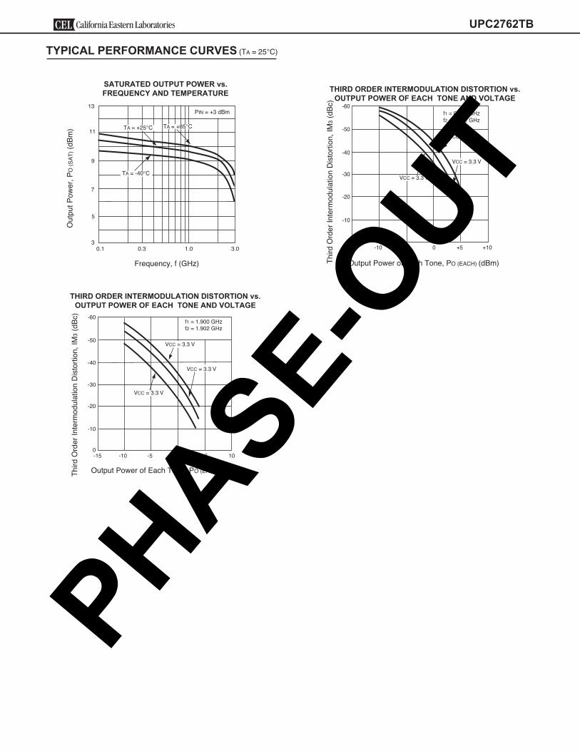
SATURATED OUTPUT POWER vs.FREQUENCY
Input Power, PIN (dBm)Input Power, PIN (dBm)
Out
put P
ower
, PO
UT (
dBm
)
Frequency, f (GHz)
Sat
urat
ed O
utpu
t Pow
er, P
O(S
AT
) (dB
m)
Out
put P
ower
, PO
UT (
dBm
)
0.1 0.3 1.0 3.0
10
0
-10
-20
-30
-40
VCC = 3.0V15
10
5
0
-5
-10-20 -15 -10 -5
f = 0.9 GHZ
VCC = 3.3V
VCC = 3.0V
VCC = 2.7V
0 +5
f = 0.9 GHzVCC = 3.0 V
10
15
5
0
-5
-10-20 -15 -10 -5 0 +5
VCC = 3.3 VVCC = 3.0 V
VCC = 2.7 V
f = 1.9 GHzVCC = 3.0 V
VCC = 3.3 V
VCC = 2.7 V
+15
+10
+5
0
-5
-10-20 -15 -10 -5 0 +5
f = 1.9 GHzVCC = 3.0 V
TA = +25°C
TA = -40°C
+15
+10
+5
0
-5
-10-20 -15 -10 -5 0 +5
TA = +85°C
Input Power, PIN (dBm)
Out
put P
ower
, PO
UT (
dBm
)
VCC = 2.7 V
VCC = 3.0 V
VCC = 3.3 V PIN = +3 dBm+13
+11
+9
+7
+5
+30.1 0.3 1.0 3.0
OUTPUT POWER vs.INPUT POWER AND TEMPERATURE
UPC2762TB
PHASE-OUT
Output Power of Each Tone, PO (EACH) (dBm)Frequency, f (GHz) Thi
rd O
rder
Inte
rmod
ulat
ion
Dis
tort
ion,
IM3
(dB
c)
Out
put P
ower
, PO
(S
AT
) (dB
m)
SATURATED OUTPUT POWER vs.FREQUENCY AND TEMPERATURE
THIRD ORDER INTERMODULATION DISTORTION vs.OUTPUT POWER OF EACH TONE AND VOLTAGE
TYPICAL PERFORMANCE CURVES (TA = 25°C)
f1 = 0.900 GHzf2 = 0.902 GHz
VCC = 3.3 V
VCC = 3.3 V
VCC = 3.3 V
-60
-50
-40
-30
-20
-10
0-15 -10 -5 0 +5 +10
PIN = +3 dBm
TA = +25°C TA = +85°C
TA = -40°C
13
11
9
7
5
30.1 0.3 1.0 3.0
f1 = 1.900 GHzf2 = 1.902 GHz
VCC = 3.3 V
VCC = 3.3 V
VCC = 3.3 V
-60
-50
-40
-30
-20
-10
0-15 -10 -5 0 +5 10
THIRD ORDER INTERMODULATION DISTORTION vs.OUTPUT POWER OF EACH TONE AND VOLTAGE
Output Power of Each Tone, PO (EACH) (dBm)Thi
rd O
rder
Inte
rmod
ulat
ion
Dis
tort
ion,
IM3
(dB
c)
UPC2762TB
PHASE-OUT
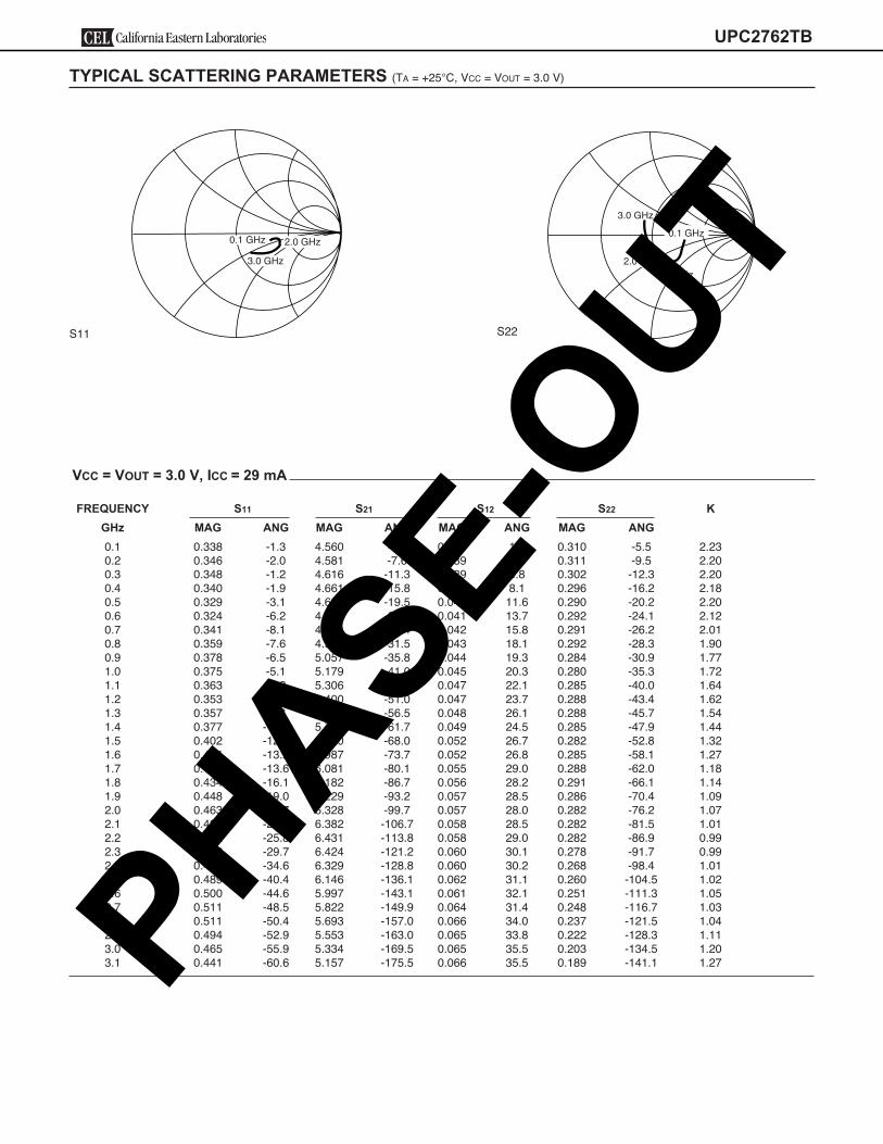
VCC = VOUT = 3.0 V, ICC = 29 mA
FREQUENCY S11 S21 S12 S22 KGHz MAG ANG MAG ANG MAG ANG MAG ANG0.1 0.338 -1.3 4.560 -3.4 0.039 1.0 0.310 -5.5 2.230.2 0.346 -2.0 4.581 -7.6 0.039 2.7 0.311 -9.5 2.200.3 0.348 -1.2 4.616 -11.3 0.039 6.8 0.302 -12.3 2.200.4 0.340 -1.9 4.661 -15.8 0.040 8.1 0.296 -16.2 2.180.5 0.329 -3.1 4.689 -19.5 0.040 11.6 0.290 -20.2 2.200.6 0.324 -6.2 4.726 -23.6 0.041 13.7 0.292 -24.1 2.120.7 0.341 -8.1 4.844 -27.4 0.042 15.8 0.291 -26.2 2.010.8 0.359 -7.6 4.927 -31.5 0.043 18.1 0.292 -28.3 1.900.9 0.378 -6.5 5.057 -35.8 0.044 19.3 0.284 -30.9 1.771.0 0.375 -5.1 5.179 -41.0 0.045 20.3 0.280 -35.3 1.721.1 0.363 -5.2 5.306 -45.9 0.047 22.1 0.285 -40.0 1.641.2 0.353 -6.7 5.400 -51.0 0.047 23.7 0.288 -43.4 1.621.3 0.357 -8.8 5.567 -56.5 0.048 26.1 0.288 -45.7 1.541.4 0.377 -11.7 5.706 -61.7 0.049 24.5 0.285 -47.9 1.441.5 0.402 -12.7 5.820 -68.0 0.052 26.7 0.282 -52.8 1.321.6 0.414 -13.2 5.987 -73.7 0.052 26.8 0.285 -58.1 1.271.7 0.426 -13.6 6.081 -80.1 0.055 29.0 0.288 -62.0 1.181.8 0.434 -16.1 6.182 -86.7 0.056 28.2 0.291 -66.1 1.141.9 0.448 -19.0 6.229 -93.2 0.057 28.5 0.286 -70.4 1.092.0 0.463 -21.7 6.328 -99.7 0.057 28.0 0.282 -76.2 1.072.1 0.483 -23.9 6.382 -106.7 0.058 28.5 0.282 -81.5 1.012.2 0.492 -25.8 6.431 -113.8 0.058 29.0 0.282 -86.9 0.992.3 0.492 -29.7 6.424 -121.2 0.060 30.1 0.278 -91.7 0.992.4 0.486 -34.6 6.329 -128.8 0.060 30.2 0.268 -98.4 1.012.5 0.489 -40.4 6.146 -136.1 0.062 31.1 0.260 -104.5 1.022.6 0.500 -44.6 5.997 -143.1 0.061 32.1 0.251 -111.3 1.052.7 0.511 -48.5 5.822 -149.9 0.064 31.4 0.248 -116.7 1.032.8 0.511 -50.4 5.693 -157.0 0.066 34.0 0.237 -121.5 1.042.9 0.494 -52.9 5.553 -163.0 0.065 33.8 0.222 -128.3 1.113.0 0.465 -55.9 5.334 -169.5 0.065 35.5 0.203 -134.5 1.203.1 0.441 -60.6 5.157 -175.5 0.066 35.5 0.189 -141.1 1.27
0.1 GHz
3.0 GHz
1.0 GHz2.0 GHz
0.1 GHz0.1 GHz
3.0 GHz
2.0 GHz
TYPICAL SCATTERING PARAMETERS (TA = +25°C, VCC = VOUT = 3.0 V)
S11 S22
UPC2762TB
PHASE-OUT
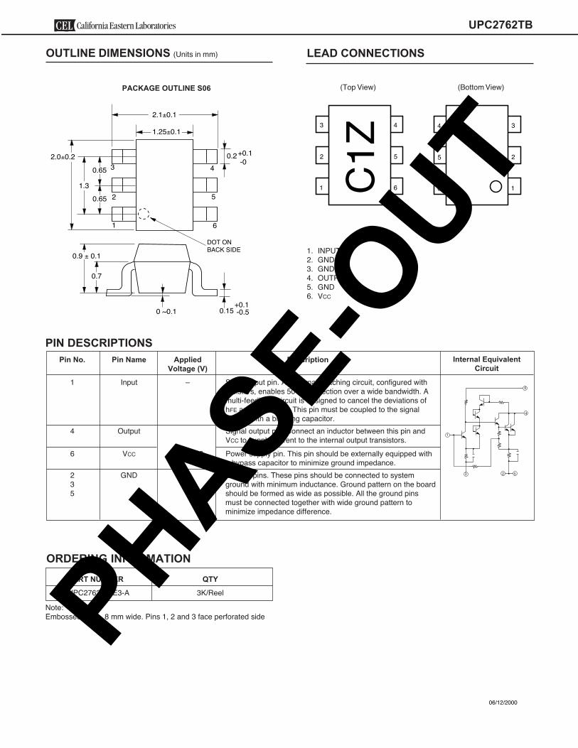
OUTLINE DIMENSIONS (Units in mm)
PACKAGE OUTLINE S06
LEAD CONNECTIONS
(Bottom View)(Top View)
1. INPUT2. GND3. GND4. OUTPUT5. GND6. VCC
ORDERING INFORMATIONYTQREBMUN TRAP
UPC2762TB-E3-A 3K/Reel
Note:Embossed Tape, 8 mm wide. Pins 1, 2 and 3 face perforated side
noitpircseDdeilppAemaN niP.oN niPVoltage (V)
1 Input – Signal input pin. An internal matching circuit, configured withresistors, enables 50 Ω connection over a wide bandwidth. Amulti-feedback circuit is designed to cancel the deviations ofhFE and resistance. This pin must be coupled to the signalsource with a blocking capacitor.
dna nip siht neewteb rotcudni na tcennoC .nip tuptuo langiStuptuO4VCC to supply current to the internal output transistors.
6 VCC 2.7 to 3.3 Power supply pin. This pin should be externally equipped witha bypass capacitor to minimize ground impedance.
2 GND 0 Ground pins. These pins should be connected to systemdraob eht no nrettap dnuorG .ecnatcudni muminim htiw dnuorg3
snip dnuorg eht llA .elbissop sa ediw sa demrof eb dluohs5must be connected together with wide ground pattern tominimize impedance difference.
PIN DESCRIPTIONSInternal Equivalent
Circuit
3
2
1
4
5
6
Z1C
3
2
1
4
5
6
+0.1-0
DOT ONBACK SIDE
+0.1 -0.50 ~0.1
0.2
0.15
3
2
1 6
5
40.65
1.3
2.0±0.2
0.65
2.1±0.1
1.25±0.1
0.9 ± 0.1
0.7
1
3 52
4
6
0002/21/60
UPC2762TB
PHASE-OUT

NOTICE
1. Descriptions of circuits, software and other related information in this document are provided only to illustrate the operation of semiconductor products andapplication examples. You are fully responsible for the incorporation of these circuits, software, and information in the design of your equipment. CaliforniaEastern Laboratories and Renesas Electronics assumes no responsibility for any losses incurred by you or third parties arising from the use of these circuits, software, or information.
2. California Eastern Laboratories has used reasonable care in preparing the information included in this document, but California Eastern Laboratories doesnot warrant that such information is error free. California Eastern Laboratories and Renesas Electronics assumes no liability whatsoever for any damagesincurred by you resulting from errors in or omissions from the information included herein.
3. California Eastern Laboratories and Renesas Electronics do not assume any liability for infringement of patents, copyrights, or other intellectual propertyrights of third parties by or arising from the use of Renesas Electronics products or technical information described in this document. No license, express,implied or otherwise, is granted hereby under any patents, copyrights or other intellectual property rights of California Eastern Laboratories or RenesasElectronics or others.
4. You should not alter, modify, copy, or otherwise misappropriate any Renesas Electronics product, whether in whole or in part. California EasternLaboratories and Renesas Electronics assume no responsibility for any losses incurred by you or third parties arising from such alteration, modification, copyor otherwise misappropriation of Renesas Electronics product.
5. Renesas Electronics products are classified according to the following two quality grades: “Standard” and “High Quality”. The recommended applicationsfor each Renesas Electronics product depends on the product’s quality grade, as indicated below. “Standard”: Computers; office equipment; communicationsequipment; test and measurement equipment; audio and visual equipment; home electronic appliances; machine tools; personal electronic equipment; and industrial robots etc. “High Quality”: Transportation equipment (automobiles, trains, ships, etc.); traffic control systems; anti-disaster systems; anti-crime systems; and safety equipment etc. Renesas Electronics products are neither intended nor authorized for use in products or systems that may pose a direct threat to human life or bodily injury (artificial life support devices or systems, surgical implantations etc.), or may cause serious property damages (nuclearreactor control systems, military equipment etc.). You must check the quality grade of each Renesas Electronics product before using it in a particularapplication. You may not use any Renesas Electronics product for any application for which it is not intended. California Eastern Laboratories and RenesasElectronics shall not be in any way liable for any damages or losses incurred by you or third parties arising from the use of any Renesas Electronics productfor which the product is not intended by California Eastern Laboratories or Renesas Electronics.
6. You should use the Renesas Electronics products described in this document within the range specified by California Eastern Laboratories, especially with respect to the maximum rating, operating supply voltage range, movement power voltage range, heat radiation characteristics, installation and other productcharacteristics. California Eastern Laboratories shall have no liability for malfunctions or damages arising out of the use of Renesas Electronics productsbeyond such specified ranges.
7. Although Renesas Electronics endeavors to improve the quality and reliability of its products, semiconductor products have specific characteristics such as the occurrence of failure at a certain rate and malfunctions under certain use conditions. Further, Renesas Electronics products are not subject to radiationresistance design. Please be sure to implement safety measures to guard them against the possibility of physical injury, and injury or damage caused by fire in the event of the failure of a Renesas Electronics product, such as safety design for hardware and software including but not limited to redundancy, fire control and malfunction prevention, appropriate treatment for aging degradation or any other appropriate measures. Because the evaluation ofmicrocomputer software alone is very difficult, please evaluate the safety of the final products or systems manufactured by you.
8. Please contact a California Eastern Laboratories sales office for details as to environmental matters such as the environmental compatibility of each Renesas Electronics product. Please use Renesas Electronics products in compliance with all applicable laws and regulations that regulate the inclusion or use of controlled substances, including without limitation, the EU RoHS Directive. California Eastern Laboratories and Renesas Electronics assume no liability for damages or losses occurring as a result of your noncompliance with applicable laws and regulations.
9. Renesas Electronics products and technology may not be used for or incorporated into any products or systems whose manufacture, use, or sale is prohibited under any applicable domestic or foreign laws or regulations. You should not use Renesas Electronics products or technology described in this document for any purpose relating to military applications or use by the military, including but not limited to the development of weapons of mass destruction. Whenexporting the Renesas Electronics products or technology described in this document, you should comply with the applicable export control laws and regulations and follow the procedures required by such laws and regulations.
10. It is the responsibility of the buyer or distributor of California Eastern Laboratories, who distributes, disposes of, or otherwise places the Renesas Electronicsproduct with a third party, to notify such third party in advance of the contents and conditions set forth in this document, California Eastern Laboratories andRenesas Electronics assume no responsibility for any losses incurred by you or third parties as a result of unauthorized use of Renesas Electronics products.
11. This document may not be reproduced or duplicated in any form, in whole or in part, without prior written consent of California Eastern Laboratories.12. Please contact a California Eastern Laboratories sales office if you have any questions regarding the information contained in this document or Renesas
Electronics products, or if you have any other inquiries.
NOTE 1: “Renesas Electronics” as used in this document means Renesas Electronics Corporation and also includes its majority-owned subsidiaries.NOTE 2: “Renesas Electronics product(s)” means any product developed or manufactured by or for Renesas Electronics.NOTE 3: Products and product information are subject to change without notice.
CEL Headquarters • 4590 Patrick Henry Drive, Santa Clara, CA 95054 • Phone (408) 919-2500 • www.cel.com
For a complete list of sales offices, representatives and distributors,Please visit our website: www.cel.com/contactusPHASE-O
UT