Bioelectric Signal Analog Front-End Module Electrocardiograph · precordial unipolar lead....
14
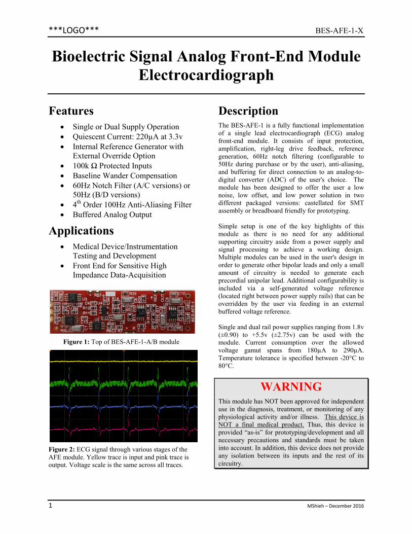
1 MShieh – December 2016 ***LOGO*** BES-AFE-1-X Bioelectric Signal Analog Front-End Module Electrocardiograph Features Single or Dual Supply Operation Quiescent Current: 220µA at 3.3v Internal Reference Generator with External Override Option 100k Ω Protected Inputs Baseline Wander Compensation 60Hz Notch Filter (A/C versions) or 50Hz (B/D versions) 4 th Order 100Hz Anti-Aliasing Filter Buffered Analog Output Applications Medical Device/Instrumentation Testing and Development Front End for Sensitive High Impedance Data-Acquisition Figure 1: Top of BES-AFE-1-A/B module Figure 2: ECG signal through various stages of the AFE module. Yellow trace is input and pink trace is output. Voltage scale is the same across all traces. Description The BES-AFE-1 is a fully functional implementation of a single lead electrocardiograph (ECG) analog front-end module. It consists of input protection, amplification, right-leg drive feedback, reference generation, 60Hz notch filtering (configurable to 50Hz during purchase or by the user), anti-aliasing, and buffering for direct connection to an analog-to- digital converter (ADC) of the user's choice. The module has been designed to offer the user a low noise, low offset, and low power solution in two different packaged versions: castellated for SMT assembly or breadboard friendly for prototyping. Simple setup is one of the key highlights of this module as there is no need for any additional supporting circuitry aside from a power supply and signal processing to achieve a working design. Multiple modules can be used in the user's design in order to generate other bipolar leads and only a small amount of circuitry is needed to generate each precordial unipolar lead. Additional configurability is included via a self-generated voltage reference (located right between power supply rails) that can be overridden by the user via feeding in an external buffered voltage reference. Single and dual rail power supplies ranging from 1.8v (±0.90) to +5.5v (±2.75v) can be used with the module. Current consumption over the allowed voltage gamut spans from 180µA to 290µA. Temperature tolerance is specified between -20°C to 80°C. WARNING This module has NOT been approved for independent use in the diagnosis, treatment, or monitoring of any physiological activity and/or illness. This device is NOT a final medical product. Thus, this device is provided “as-is” for prototyping/development and all necessary precautions and standards must be taken into account. In addition, this device does not provide any isolation between its inputs and the rest of its circuitry.
-
Upload
trinhthien -
Category
Documents
-
view
236 -
download
1
Transcript of Bioelectric Signal Analog Front-End Module Electrocardiograph · precordial unipolar lead....
1 MShieh – December 2016
***LOGO*** BES-AFE-1-X
Bioelectric Signal Analog Front-End Module Electrocardiograph
Features Single or Dual Supply Operation Quiescent Current: 220µA at 3.3v Internal Reference Generator with
External Override Option 100k Ω Protected Inputs Baseline Wander Compensation 60Hz Notch Filter (A/C versions) or
50Hz (B/D versions) 4th Order 100Hz Anti-Aliasing Filter Buffered Analog Output
Applications Medical Device/Instrumentation
Testing and Development Front End for Sensitive High
Impedance Data-Acquisition
Figure 1: Top of BES-AFE-1-A/B module
Figure 2: ECG signal through various stages of the AFE module. Yellow trace is input and pink trace is output. Voltage scale is the same across all traces.
Description
The BES-AFE-1 is a fully functional implementation of a single lead electrocardiograph (ECG) analog front-end module. It consists of input protection, amplification, right-leg drive feedback, reference generation, 60Hz notch filtering (configurable to 50Hz during purchase or by the user), anti-aliasing, and buffering for direct connection to an analog-to-digital converter (ADC) of the user's choice. The module has been designed to offer the user a low noise, low offset, and low power solution in two different packaged versions: castellated for SMT assembly or breadboard friendly for prototyping. Simple setup is one of the key highlights of this module as there is no need for any additional supporting circuitry aside from a power supply and signal processing to achieve a working design. Multiple modules can be used in the user's design in order to generate other bipolar leads and only a small amount of circuitry is needed to generate each precordial unipolar lead. Additional configurability is included via a self-generated voltage reference (located right between power supply rails) that can be overridden by the user via feeding in an external buffered voltage reference. Single and dual rail power supplies ranging from 1.8v (±0.90) to +5.5v (±2.75v) can be used with the module. Current consumption over the allowed voltage gamut spans from 180µA to 290µA. Temperature tolerance is specified between -20°C to 80°C.
WARNING This module has NOT been approved for independent use in the diagnosis, treatment, or monitoring of any physiological activity and/or illness. This device is NOT a final medical product. Thus, this device is provided “as-is” for prototyping/development and all necessary precautions and standards must be taken into account. In addition, this device does not provide any isolation between its inputs and the rest of its circuitry.
***Company Name***
2
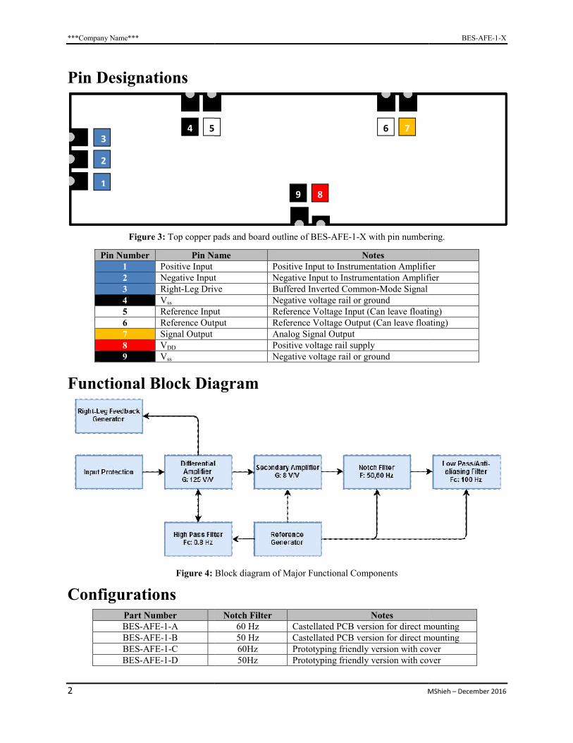
Pin Designations
Figure 3: Top copper pads
Pin Number Pin Name1 Positive Input 2 Negative Input3 Right-Leg Drive4 Vss 5 Reference Input6 Reference Output7 Signal Output 8 VDD 9 Vss
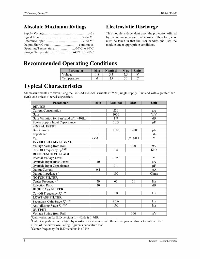
Functional Block Diagram
Figure 4:
Configurations Part Number BES-AFE-1-A BES-AFE-1-B BES-AFE-1-C BES-AFE-1-D
1
2
3 4 5
MS
pads and board outline of BES-AFE-1-X with pin numbering
Pin Name Notes Positive Input to Instrumentation Amplifier
Negative Input Negative Input to Instrumentation AmplifierLeg Drive Buffered Inverted Common-Mode Signal
Negative voltage rail or ground Input Reference Voltage Input (Can leave floating
Reference Output Reference Voltage Output (Can leave floating) Analog Signal Output
Positive voltage rail supply Negative voltage rail or ground
Functional Block Diagram
Block diagram of Major Functional Components
Notch Filter Notes 60 Hz Castellated PCB version for direct mounting50 Hz Castellated PCB version for direct mounting60Hz Prototyping friendly version with cover50Hz Prototyping friendly version with cover
6 7
8 9
BES-AFE-1-X
MShieh – December 2016
with pin numbering.
Positive Input to Instrumentation Amplifier Negative Input to Instrumentation Amplifier
floating) (Can leave floating)
version for direct mounting version for direct mounting
with cover with cover
***Company Name*** BES-AFE-1-X
3 MShieh – December 2016
Absolute Maximum Ratings Supply Voltage…………………………………...+7v Signal Input………………………………....V- to V+ Reference Input……………………………..V- to V+ Output Short Circuit…………………….. continuous Operating Temperature…………… ….-20°C to 80°C Storage Temperature………………...-40°C to 120°C
Electrostatic Discharge This module is dependent upon the protection offered by the semiconductors that it uses. Therefore, care must be taken in that the user handles and uses the module under appropriate conditions.
Recommended Operating Conditions Parameter Min Nominal Max Units
Voltage 1.8 3.3 5.5 V Temperature 0 25 50 C
Typical Characteristics All measurements are taken using the BES-AFE-1-A/C variants at 25°C, single supply 3.3v, and with a greater than 1MΩ load unless otherwise specified.
Parameter Min Nominal Max Unit DEVICE Current Consumption 220 µA Gain 1000 V/V Gain Variation for Passband of 1 - 40Hz 1 1.8 dB Power Supply Input Capacitance 10.5 µF SIGNAL INPUT Bias Current ±100 ±200 pA Impedance 1 GΩ VCM (V-)+0.1 (V+)-0.1 V INVERTED CMV SIGNAL Voltage Swing from Rail 100 mV
Cut-Off Frequency 4.8 KHz
REFERENCE VOLTAGE Internal Voltage Level 1.65 V Override Input Bias Current 10 µA Override Input Capacitance 0.1 µF Output Current 0.1 mA Output Impedance 2 100 Ohms NOTCH FILTER Center Frequency 3 59 60 61 Hz Rejection Ratio 20 dB HIGH PASS FILTER
Cut-Off Frequency 0.8 Hz
LOWPASS FILTER
Secondary Gain Stage 96.6 Hz
Anti-aliasing Stage 100 Hz
OUTPUT Voltage Swing from Rail 100 mV
1Gain variation for B/D versions 1 – 40Hz is 1.9dB. 2Output impedance is dictated by resistor R25 in series with the virtual ground driver to mitigate the effect of the driver oscillating if given a capacitive load. 3Center frequency for B/D versions is 50 Hz
***Company Name*** BES-AFE-1-X
4 MShieh – December 2016
Performance Graphs
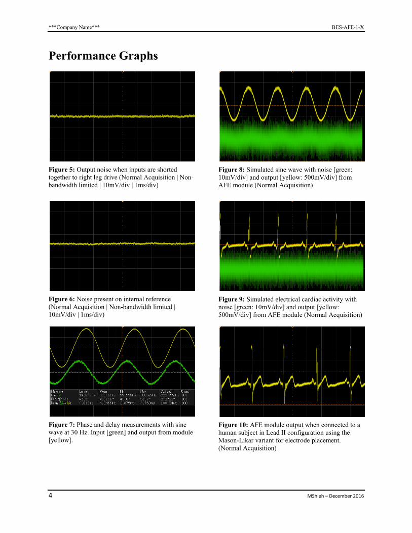
Figure 5: Output noise when inputs are shorted together to right leg drive (Normal Acquisition | Non-bandwidth limited | 10mV/div | 1ms/div)
Figure 6: Noise present on internal reference (Normal Acquisition | Non-bandwidth limited | 10mV/div | 1ms/div)
Figure 7: Phase and delay measurements with sine wave at 30 Hz. Input [green] and output from module [yellow].
Figure 8: Simulated sine wave with noise [green: 10mV/div] and output [yellow: 500mV/div] from AFE module (Normal Acquisition)
Figure 9: Simulated electrical cardiac activity with noise [green: 10mV/div] and output [yellow: 500mV/div] from AFE module (Normal Acquisition)
Figure 10: AFE module output when connected to a human subject in Lead II configuration using the Mason-Likar variant for electrode placement. (Normal Acquisition)
***Company Name*** BES-AFE-1-X
5 MShieh – December 2016
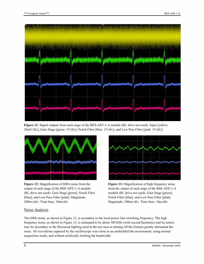
Figure 11: Signal outputs from each stage of the BES-AFE-1-A module (RL drive not used). Input [yellow:
20mV/div], Gain Stage [green: 1V/div], Notch Filter [blue: 1V/div], and Low Pass Filter [pink: 1V/div]
Figure 12: Magnification of 60Hz noise from the
output of each stage of the BSE-AFE-1-A module
(RL drive not used). Gain Stage [green], Notch Filter
[blue], and Low Pass Filter [pink]. Magnitude:
200mv/div. Time base: 10ms/div
Figure 13: Magnification of high frequency noise
from the output of each stage of the BSE-AFE-1-A
module (RL drive not used). Gain Stage [green],
Notch Filter [blue], and Low Pass Filter [pink].
Magnitude: 200mv/div. Time base: 10µs/div
Noise Analysis
The 60Hz noise, as shown in Figure 12, is secondary to the local power line switching frequency. The high
frequency noise, as shown in Figure 13, is estimated to be about 100 KHz (with second harmonic) and its source
may be secondary to the florescent lighting used in the test area as turning off the fixtures greatly attenuated the
noise. All waveforms captured by the oscilloscope were done in an unshielded lab environment, using normal
acquisition mode, and without artificially limiting the bandwidth.
***Company Name*** BES-AFE-1-X
6 MShieh – December 2016
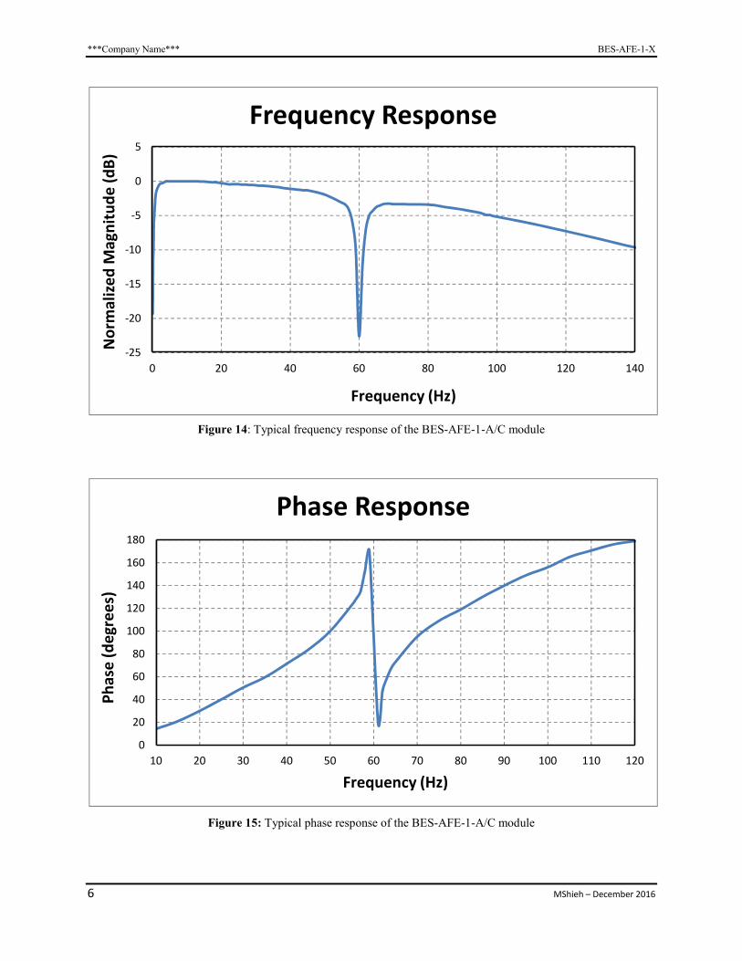
Figure 14: Typical frequency response of the BES-AFE-1-A/C module
Figure 15: Typical phase response of the BES-AFE-1-A/C module
-25
-20
-15
-10
-5
0
5
0 20 40 60 80 100 120 140
No
rmal
ize
d M
agn
itu
de
(dB
)
Frequency (Hz)
Frequency Response
0
20
40
60
80
100
120
140
160
180
10 20 30 40 50 60 70 80 90 100 110 120
Ph
ase
(d
egr
ee
s)
Frequency (Hz)
Phase Response

***Company Name*** BES-AFE-1-X
7 MShieh – December 2016
Figure 16: Typical frequency response of the BES-AFE-1-B/D module
Figure 17: Typical phase response of the BES-AFE-1-B/D module
-30
-25
-20
-15
-10
-5
0
5
0 25 50 75 100 125 150
No
rmal
ize
d M
agn
itu
de
(dB
)
Frequency (Hz)
Frequency Response
0
20
40
60
80
100
120
140
160
180
10 20 30 40 50 60 70 80 90 100 110 120
Ph
ase
(d
egr
ee
s)
Frequency (Hz)
Phase Response

***Company Name*** BES-AFE-1-X
8 MShieh – December 2016
Figure 18: Current Consumption of a AFE Module with inputs shorted to right leg drive and 1MΩ load on output
***TO-DO***
Figure 19: ***TO-DO***
150
170
190
210
230
250
270
290
310
1.50 2.00 2.50 3.00 3.50 4.00 4.50 5.00 5.50
Cu
rre
nt
(uA
)
Supply Voltage (V)
Current Consumption of BES-AFE-1 Module

***Company Name*** BES-AFE-1-X
9 MShieh – December 2016
Application Examples
Quick Setup for Frontal “Bipolar” Leads with Internal Reference
As shown in the figure below, very few components are needed to quickly set up and run the BES-AFE-1-X module. The inputs are shown on the left via an adapter board which allows the module to accept DIN42802 (1.5mm pin diameter) shrouded medical connectors. The external reference input is left open as the module generates its own internal reference centered between the voltage rails, and the power supply inputs can be without decoupling capacitors as onboard decoupling is provided. The output is directly connected to an analog-to-digital converter.
Figure 20: BES-AFE-1-C/D Module Hookup for Frontal Lead Configuration. See appendix for more information.
Quick Setup for Precordial “Unipolar” Leads with Internal Reference
The precordial leads ( − ), generated by the electrocardiograph, represent the horizontal plane of the heart – the plane orthogonal to the view provided by the six frontal leads. To generate such a lead, the precordial electrode is regarded as the positive pole and the Wilson Central Terminal is the negative pole. The Wilson Central Terminal is the arithmetic average of the limb electrodes LA, RA, and LL. Please see appendix at the end for more information.
Figure 21: Schematic for Precordial Lead Configuration
***Company Name*** BES-AFE-1-X
10 MShieh – December 2016
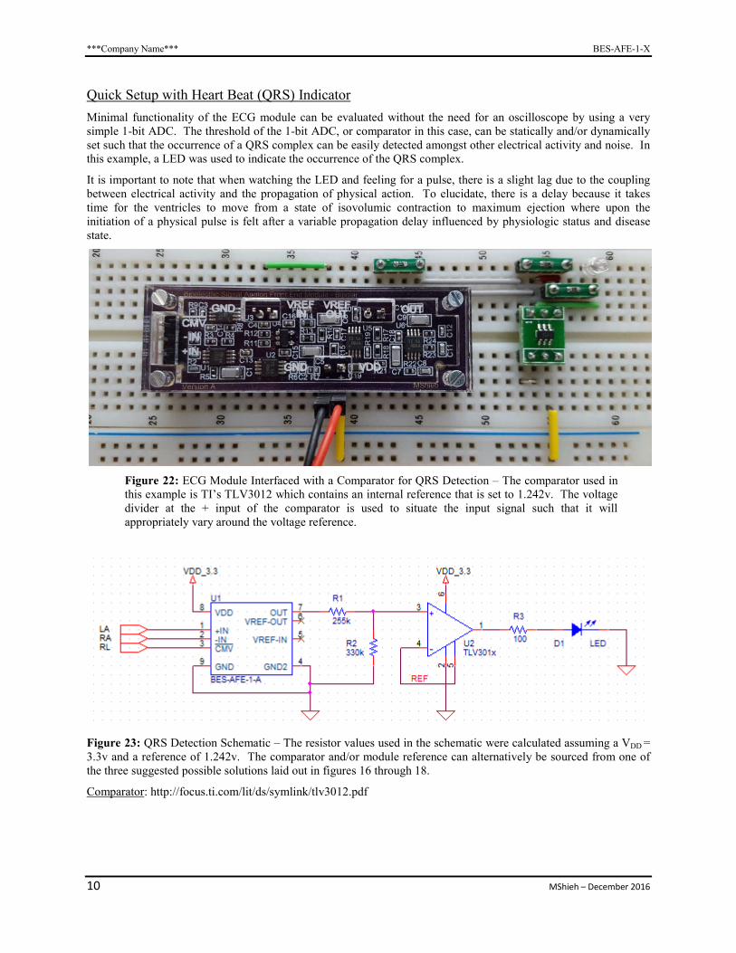
Quick Setup with Heart Beat (QRS) Indicator
Minimal functionality of the ECG module can be evaluated without the need for an oscilloscope by using a very simple 1-bit ADC. The threshold of the 1-bit ADC, or comparator in this case, can be statically and/or dynamically set such that the occurrence of a QRS complex can be easily detected amongst other electrical activity and noise. In this example, a LED was used to indicate the occurrence of the QRS complex.
It is important to note that when watching the LED and feeling for a pulse, there is a slight lag due to the coupling between electrical activity and the propagation of physical action. To elucidate, there is a delay because it takes time for the ventricles to move from a state of isovolumic contraction to maximum ejection where upon the initiation of a physical pulse is felt after a variable propagation delay influenced by physiologic status and disease state.
Figure 22: ECG Module Interfaced with a Comparator for QRS Detection – The comparator used in this example is TI’s TLV3012 which contains an internal reference that is set to 1.242v. The voltage divider at the + input of the comparator is used to situate the input signal such that it will appropriately vary around the voltage reference.
Figure 23: QRS Detection Schematic – The resistor values used in the schematic were calculated assuming a VDD = 3.3v and a reference of 1.242v. The comparator and/or module reference can alternatively be sourced from one of the three suggested possible solutions laid out in figures 16 through 18.
Comparator: http://focus.ti.com/lit/ds/symlink/tlv3012.pdf
***Company Name*** BES-AFE-1-X
11 MShieh – December 2016
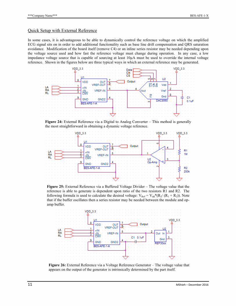
Quick Setup with External Reference
In some cases, it is advantageous to be able to dynamically control the reference voltage on which the amplified ECG signal sits on in order to add additional functionality such as base line drift compensation and QRS saturation avoidance. Modification of the board itself (remove C4) or an inline series resistor may be needed depending upon the voltage source used and how fast the reference voltage must change during operation. In any case, a low impedance voltage source that is capable of sourcing at least 10µA must be used to override the internal voltage reference. Shown in the figures below are three typical ways in which an external reference may be generated.
Figure 24: External Reference via a Digital to Analog Converter – This method is generally the most straightforward in obtaining a dynamic voltage reference.
Figure 25: External Reference via a Buffered Voltage Divider – The voltage value that the reference is able to generate is dependent upon ratio of the two resistors R1 and R2. The following formula is used to calculate the desired voltage: VRef = Vdd*(R2/ (R1 + R2)). Note that if the buffer oscillates then a series resistor may be needed between the module and op-amp buffer.
Figure 26: External Reference via a Voltage Reference Generator – The voltage value that appears on the output of the generator is intrinsically determined by the part itself.

***Company Name*** BES-AFE-1-X
12 MShieh – December 2016
Parameter Setting All resistors are 0402 sized thick-film with exception of R15 – R20 which are thin films. All capacitors are either C0G or X5R/X7R (EIA Class-1 or Class-2) dielectric material for signal path or decoupling respectively. Resistor values are in ohms, and capacitor values are in farads unless otherwise specified.
Virtual Ground
Although the module is fully capable of intrinsically setting its virtual ground to approximately ½(VDD-VSS), there may be instances in which the user or controlling system needs to dynamically vary it. Dynamic variation is made possible by providing a low impedance voltage source to the “REF IN” pin of the module as illustrated in the “Quick Setup with External Reference” example. Note that the removal of C4, a decoupling capacitor, may need to be done to avoid instability of the voltage source (op-amp) and/or severe bandwidth limiting. In the case where an external reference is not needed, C4 can be left alone to reduce noise that is normally present on the internal reference due to variations in the power supply and Johnson noise generated by the high value resistors. In addition, one can attach additional capacitance to the “REF IN” pin for further noise reduction and increase the PSRR.
Gain
The overall gain of the module is set at default to about 1000V/V. The bulk of this gain is contributed by the instrumentation amplifier U1 in order to maximize CMRR. The gain of this primary stage is 125V/V. The secondary gain stage, U2B, contributes additional gain to increase the overall gain. The ratio of two nearby resistors, R6 and R7, dictate the amount of gain that this op-amp provides to the module. A change in gain provided by U4B requires either a change in value for R6 or R7. Alternatively, resistors R3 and R4, which dictates the gain of the instrumentation amplifier, may be changed as well. Selection of which resistor to change is primarily dictated by whether one wishes to increase or decrease the gain of the overall system at the expense of some other parameter(s). One example would be if one were to increase the gain by decreasing the value of R7. An advantage of making such a change would be that Johnson noise contributed by R7 itself would be less. A disadvantage, however, would be that the current required by the module would slightly increase. Note that changing the value of R6 will also change the antialiasing filter’s cutoff frequency since the secondary stage is bandwidth limited.
= = 1 +
= = 1 + 100
+
= ∗
Antialiasing/Low Pass Filter Cut-Off Frequency
The antialiasing/low-pass filter is a 4th order system that is composed of two separate 2nd order Sallen-Key Filters. Adjusting the cut-off frequency can either be done by changing the resistors or capacitors of each section. Note that the overall cut-off frequency of the system will not be the cut-off frequency of each individual 2nd order stage as their attenuations will add. To compensate, each stage’s Q-factor must be adjusted so that the pass band is flat while achieving the correct cut-off frequency. The calculations required can be done by hand but calculators/simulators, which can be found on the internet for free, are available to make this task fast and straight-forward such as Analog Devices’ Analog Filter Wizard.
***Company Name*** BES-AFE-1-X
13 MShieh – December 2016
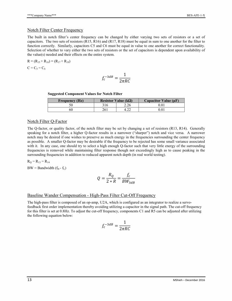
Notch Filter Center Frequency
The built in notch filter’s center frequency can be changed by either varying two sets of resistors or a set of capacitors. The two sets of resistors (R15, R16) and (R17, R18) must be equal in sum to one another for the filter to function correctly. Similarly, capacitors C5 and C6 must be equal in value to one another for correct functionality. Selection of whether to vary either the two sets of resistors or the set of capacitors is dependent upon availability of the value(s) needed and their effects on the entire system.
R = (R15 + R16) = (R17 + R18)
C = C5 = C6
=
1
2
Suggested Component Values for Notch Filter
Frequency (Hz) Resistor Value (kΩ) Capacitor Value (µF) 50 316 2.26 0.01 60 261 4.22 0.01
Notch Filter Q-Factor
The Q-factor, or quality factor, of the notch filter may be set by changing a set of resistors (R13, R14). Generally speaking for a notch filter, a higher Q-factor results in a narrower (“sharper”) notch and vice versa. A narrower notch may be desired if one wishes to preserve as much energy in the frequencies surrounding the center frequency as possible. A smaller Q-factor may be desirable if the frequency to be rejected has some small variance associated with it. In any case, one should try to select a high enough Q-factor such that very little energy of the surrounding frequencies is removed while maintaining filter response though not exceedingly high as to cause peaking in the surrounding frequencies in addition to reduced apparent notch depth (in real world testing).
RQ = R13 = R14
BW = Bandwidth (fH - fL)
=
2 ∗ =
Baseline Wander Compensation - High-Pass Filter Cut-Off Frequency
The high-pass filter is composed of an op-amp, U2A, which is configured as an integrator to realize a servo-feedback first order implementation thereby avoiding utilizing a capacitor in the signal path. The cut-off frequency for this filter is set at 0.8Hz. To adjust the cut-off frequency, components C1 and R5 can be adjusted after utilizing the following equation below:
=
1
2
***Company Name*** BES-AFE-1-X
14 MShieh – December 2016
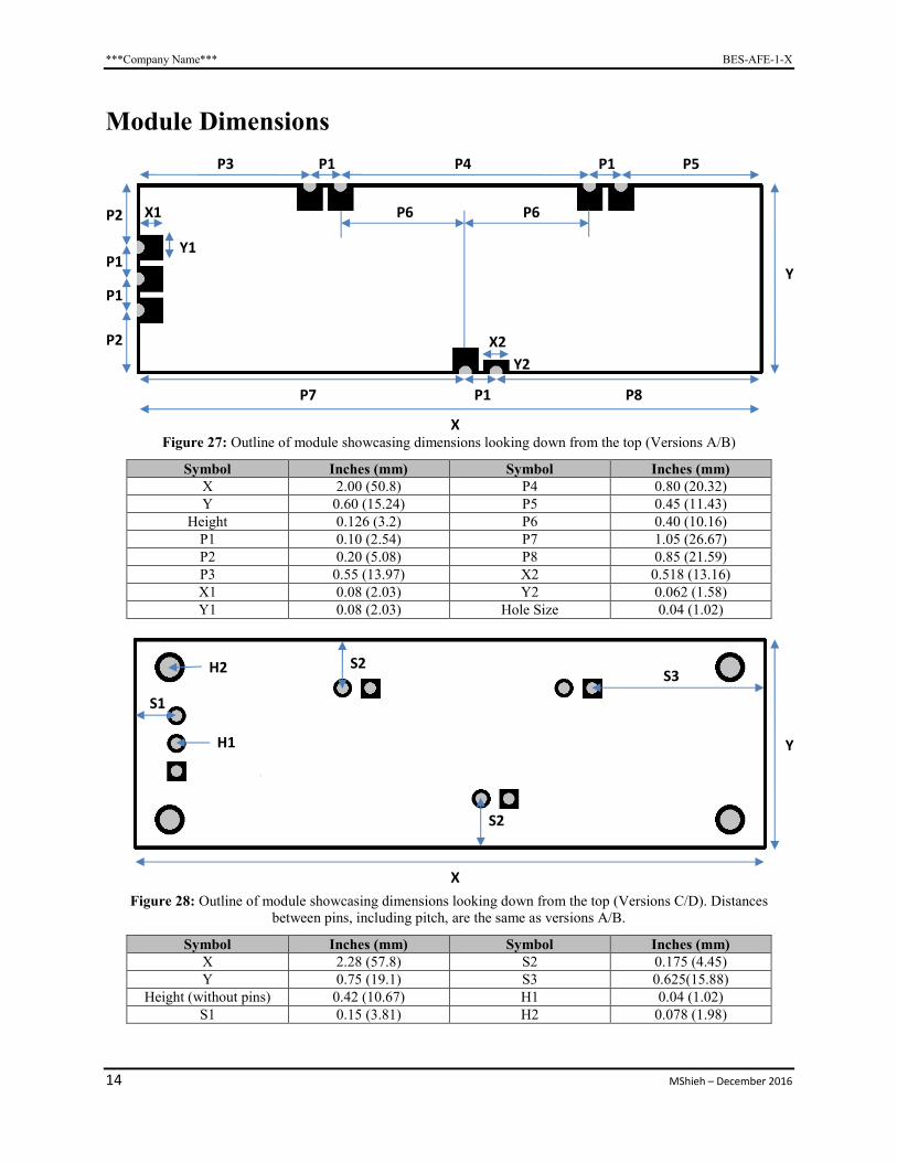
Module Dimensions
Figure 27: Outline of module showcasing dimensions looking down from the top (Versions A/B)
Symbol Inches (mm) Symbol Inches (mm) X 2.00 (50.8) P4 0.80 (20.32) Y 0.60 (15.24) P5 0.45 (11.43)
Height 0.126 (3.2) P6 0.40 (10.16) P1 0.10 (2.54) P7 1.05 (26.67) P2 0.20 (5.08) P8 0.85 (21.59) P3 0.55 (13.97) X2 0.518 (13.16) X1 0.08 (2.03) Y2 0.062 (1.58) Y1 0.08 (2.03) Hole Size 0.04 (1.02)
Figure 28: Outline of module showcasing dimensions looking down from the top (Versions C/D). Distances between pins, including pitch, are the same as versions A/B.
Symbol Inches (mm) Symbol Inches (mm) X 2.28 (57.8) S2 0.175 (4.45) Y 0.75 (19.1) S3 0.625(15.88)
Height (without pins) 0.42 (10.67) H1 0.04 (1.02) S1 0.15 (3.81) H2 0.078 (1.98)
S2
S1
S2
X2
Y2
Y1
X1
P1
P1
P1
P2
P1
P1
X
Y
P2
P3 P4 P5
P6
P7 P8
P6
X
Y
S3 H2
H1