Architecture of 8085 MPU presentation1 -...
25
1 TK2633 TK2633 8085 Microprocessor Architecture 8085 Microprocessor Architecture DR MASRI AYOB
Transcript of Architecture of 8085 MPU presentation1 -...
1
TK2633 TK2633
8085 Microprocessor Architecture
8085 Microprocessor Architecture
DR MASRI AYOB
2
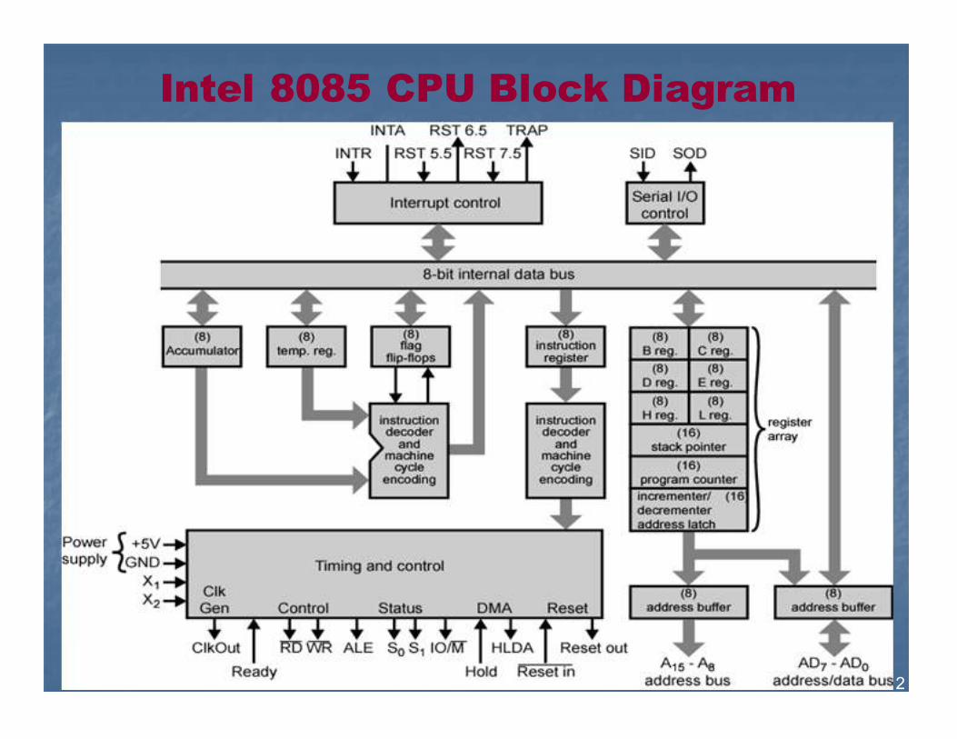
Intel 8085 CPU Block Diagram
3
� Registers – hold temporary data.
� Instruction register (IR)– holds the currently executing instruction.
� Instruction Decoder (ID)- decodes the instruction. Once decoded, the instruction controls the remainder of the MPU, memory and IO through the timing and control block.
The 8085 Block Diagram
4
� Temporary register- holds information from the memory or register array. An input of the ALU.
� Increment/Decrement address latch – It adds or subtracts one from any of other registers in register array.
The 8085 Block Diagram
Why are the PC and SP registers are 16-bit ?
5
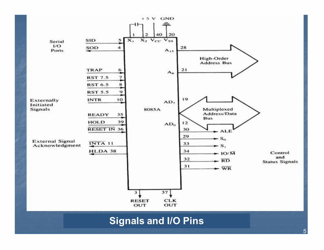
Signals and I/O Pins
6
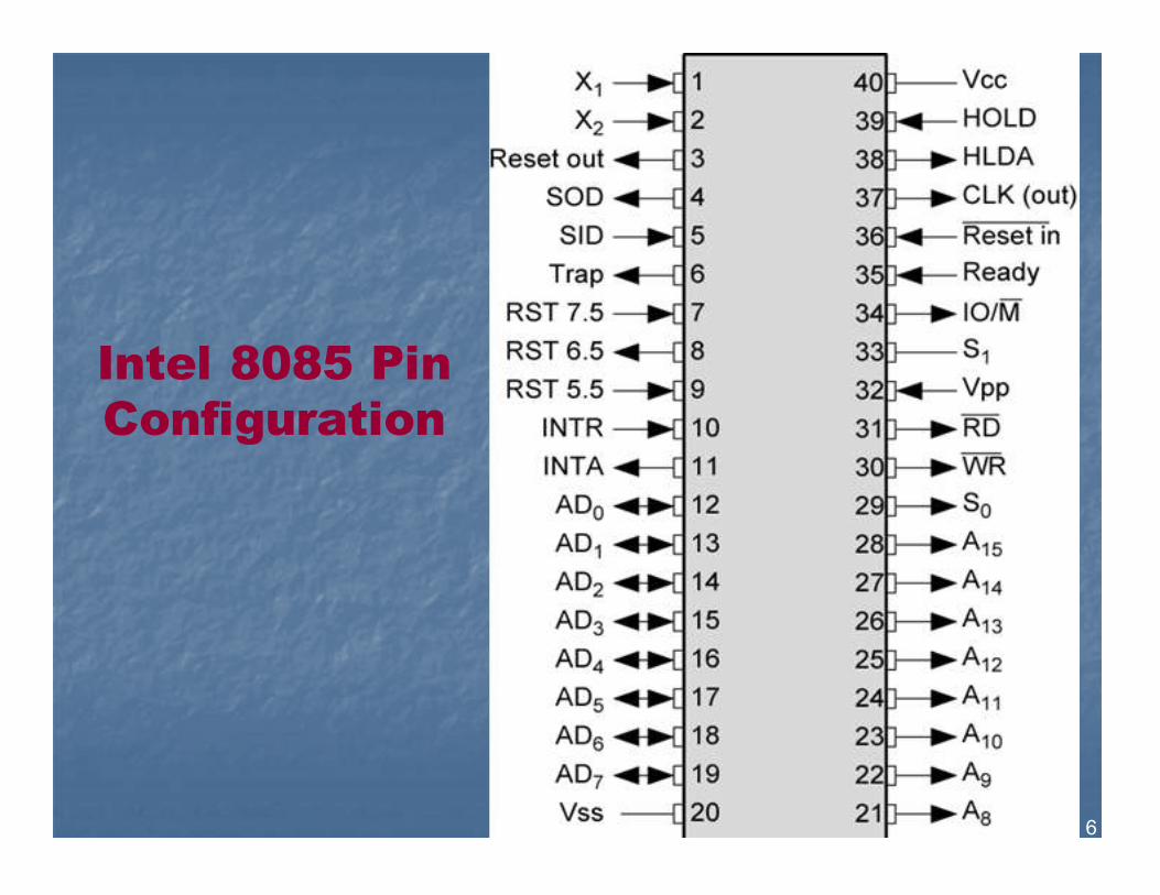
Intel 8085 Pin
Configuration
7
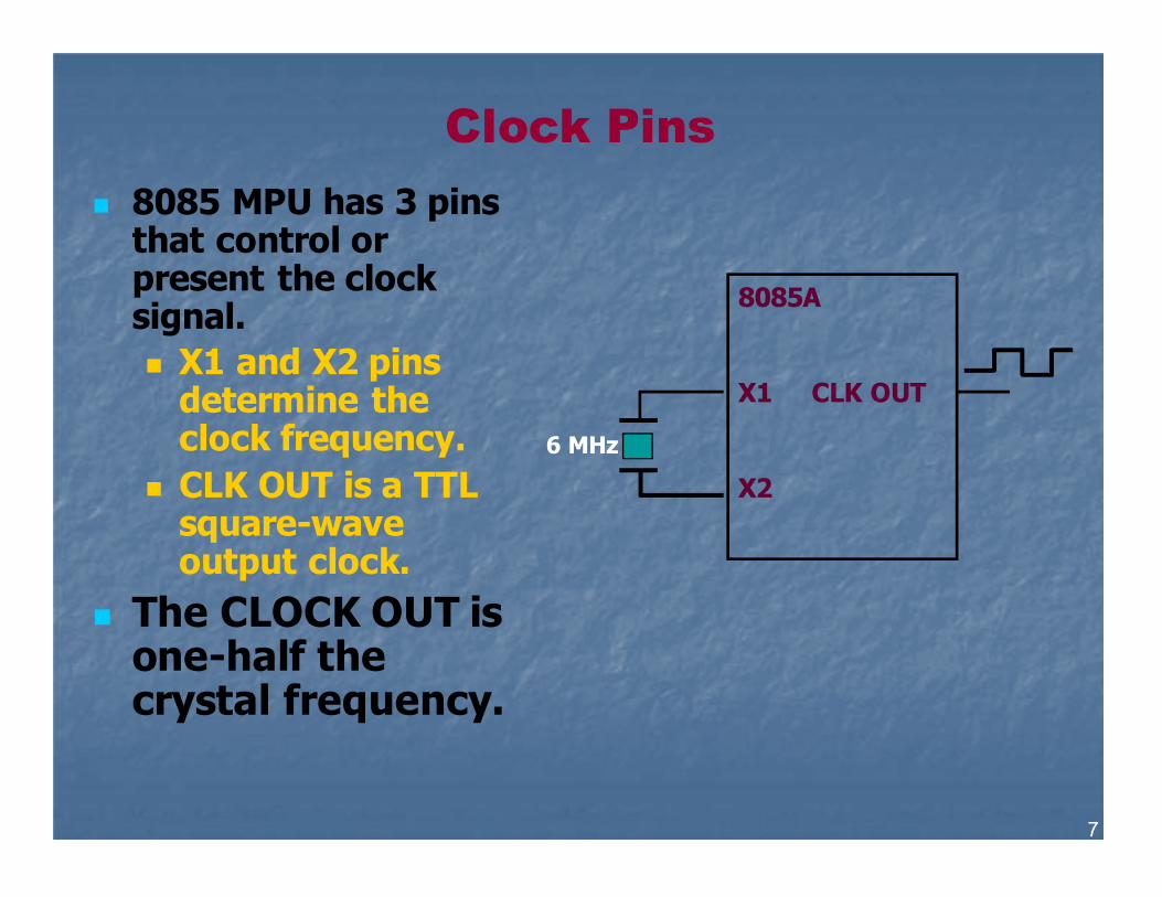
� 8085 MPU has 3 pins that control or present the clock signal.
� X1 and X2 pins determine the clock frequency.
� CLK OUT is a TTL square-wave output clock.
� The CLOCK OUT is one-half the crystal frequency.
Clock Pins
8085A
X1 CLK OUT
X2
6 MHz
8
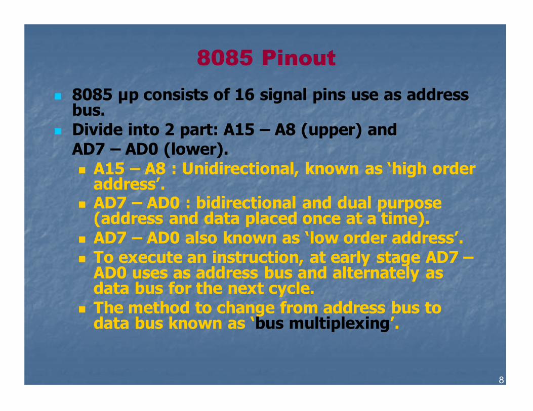
� 8085 μp consists of 16 signal pins use as address bus.
� Divide into 2 part: A15 – A8 (upper) and AD7 – AD0 (lower).
� A15 – A8 : Unidirectional, known as ‘high order address’.
� AD7 – AD0 : bidirectional and dual purpose (address and data placed once at a time).
� AD7 – AD0 also known as ‘low order address’. � To execute an instruction, at early stage AD7 –
AD0 uses as address bus and alternately as data bus for the next cycle.
� The method to change from address bus to data bus known as ‘bus multiplexing’.
8085 Pinout
9
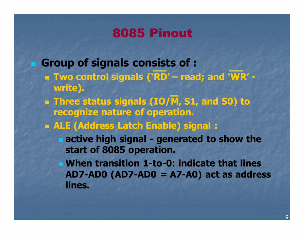
� Group of signals consists of :
� Two control signals (‘RD’ – read; and ‘WR’ - write).
� Three status signals (IO/M, S1, and S0) to recognize nature of operation.
� ALE (Address Latch Enable) signal :
� active high signal - generated to show the start of 8085 operation.
� When transition 1-to-0: indicate that lines AD7-AD0 (AD7-AD0 = A7-A0) act as address lines.
8085 Pinout
10
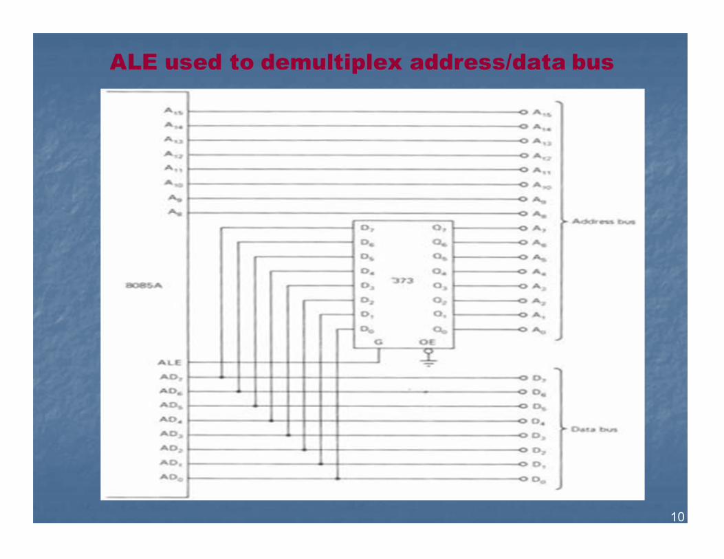
ALE used to demultiplex address/data bus
11
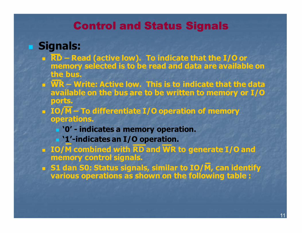
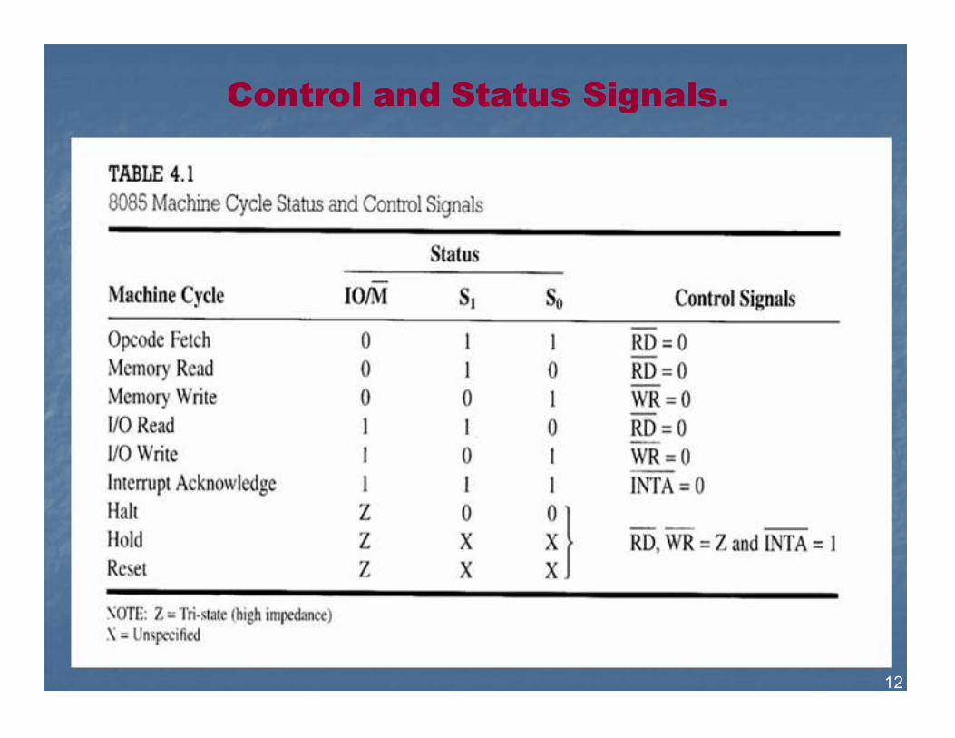
Control and Status Signals Control and Status Signals
� Signals: � RD – Read (active low). To indicate that the I/O or
memory selected is to be read and data are available on the bus.
� WR – Write: Active low. This is to indicate that the data available on the bus are to be written to memory or I/O ports.
� IO/M – To differentiate I/O operation of memory operations.
� ‘0’ - indicates a memory operation.
� ‘1’-indicates an I/O operation.
� IO/M combined with RD and WR to generate I/O and memory control signals.
� S1 dan S0: Status signals, similar to IO/M, can identify various operations as shown on the following table :
12
Control and Status Signals. Control and Status Signals.
13
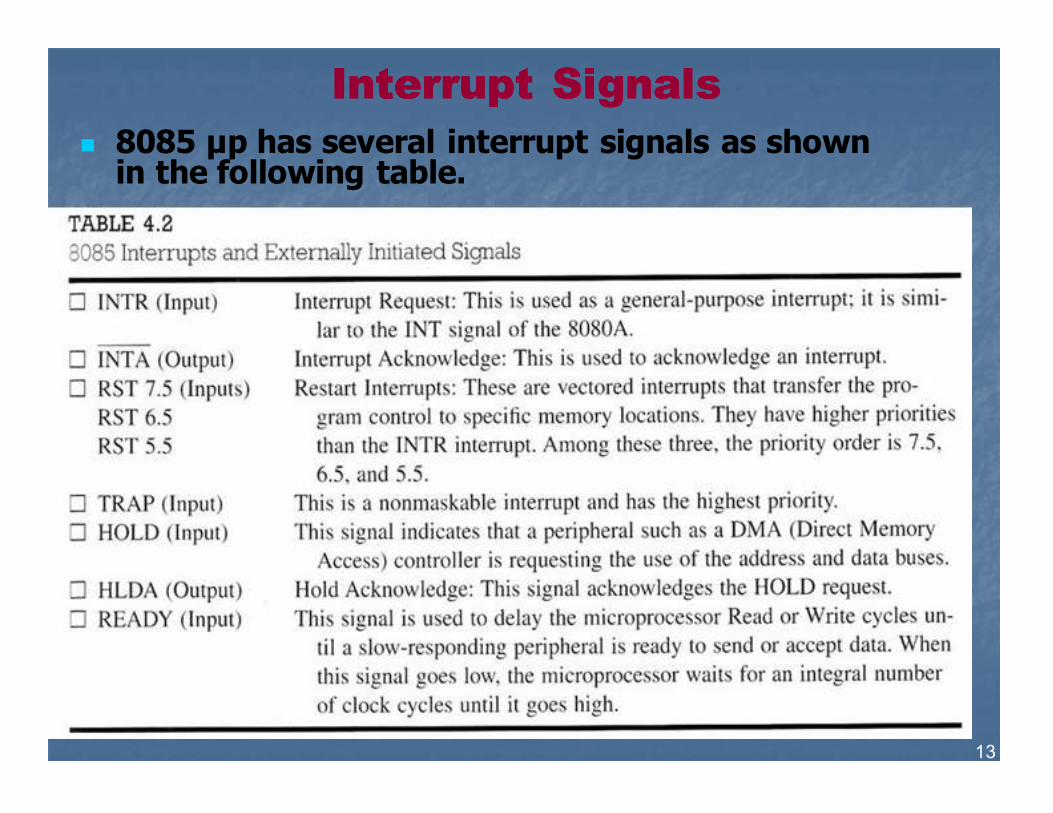
Interrupt Signals Interrupt Signals
� 8085 μp has several interrupt signals as shown in the following table.
14
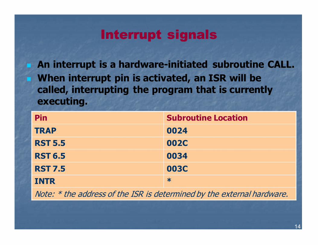
Interrupt signals Interrupt signals
� An interrupt is a hardware-initiated subroutine CALL.
� When interrupt pin is activated, an ISR will be called, interrupting the program that is currently executing.
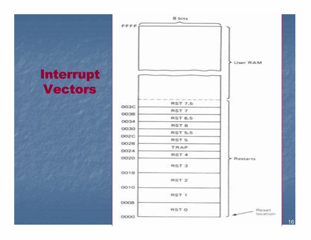
Pin Subroutine Location
TRAP 0024
RST 5.5 002C
RST 6.5 0034
RST 7.5 003C
INTR *
Note: * the address of the ISR is determined by the external hardware.
15
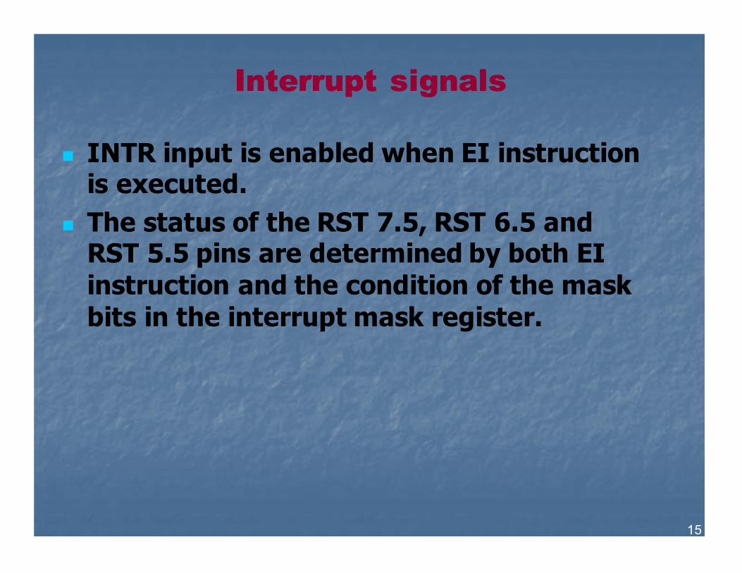
Interrupt signals Interrupt signals
� INTR input is enabled when EI instruction is executed.
� The status of the RST 7.5, RST 6.5 and RST 5.5 pins are determined by both EI
instruction and the condition of the mask
bits in the interrupt mask register.
16
Interrupt
Vectors
Interrupt
Vectors
17
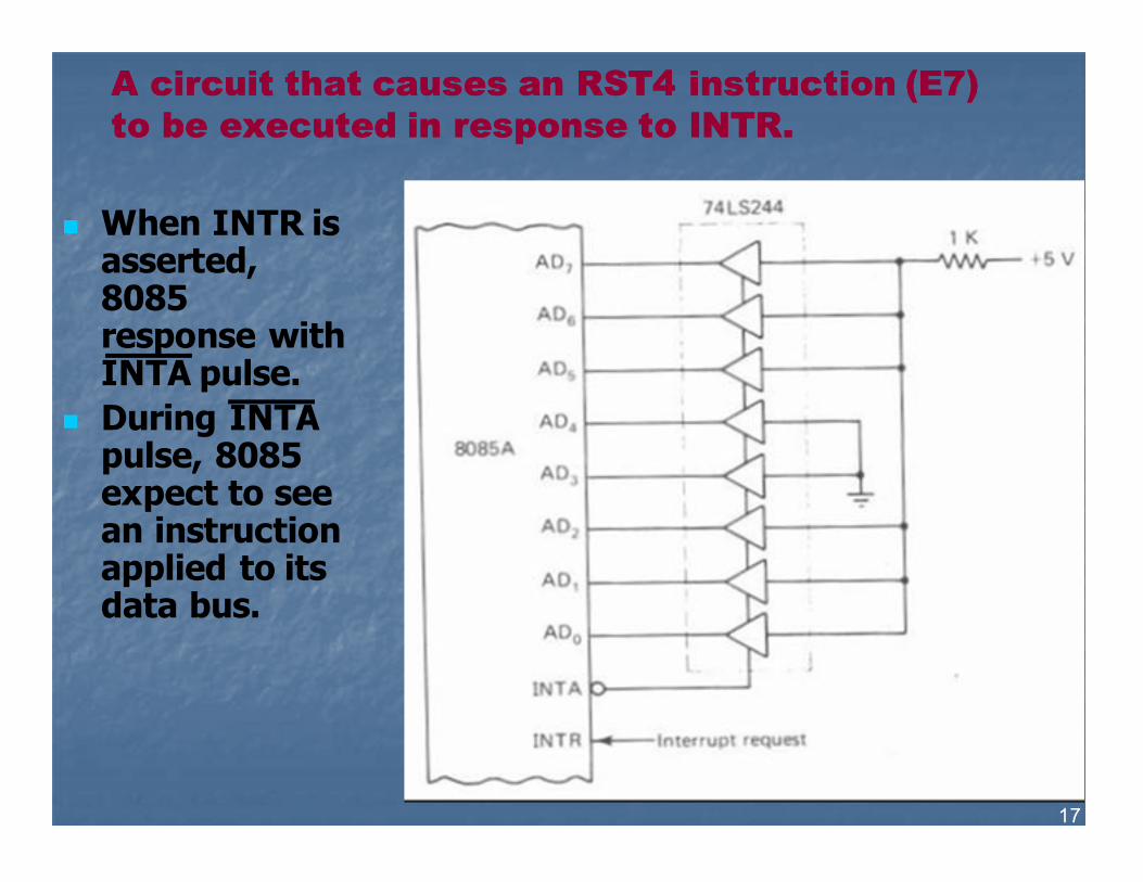
A circuit that causes an RST4 instruction (E7)
to be executed in response to INTR.
A circuit that causes an RST4 instruction (E7)
to be executed in response to INTR.
� When INTR is asserted, 8085 response with INTA pulse.
� During INTA pulse, 8085 expect to see an instruction applied to its data bus.
18
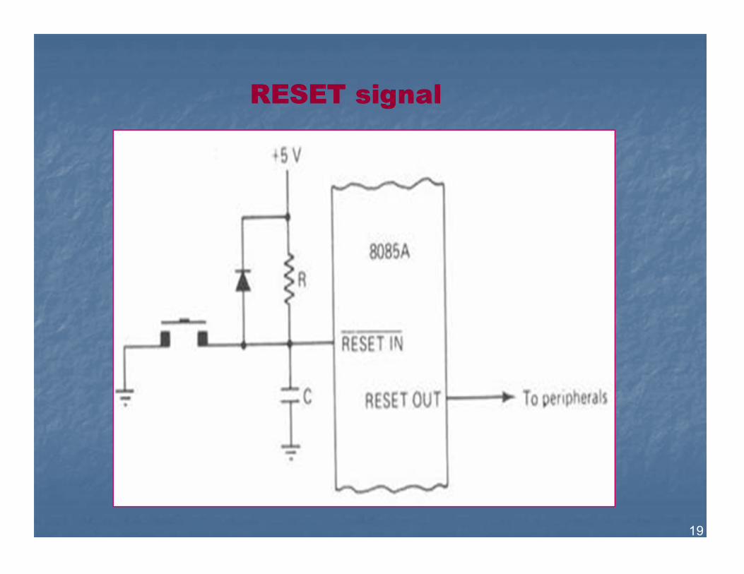
RESET signal RESET signal
� Following are the two kind of RESET signals:
� RESET IN: an active low input signal, Program Counter (PC) will be set to 0 and thus MPU will reset.
� RESET OUT: an output reset signal to indicate that the μp was reset (i.e. RESET IN=0). It also used to reset external devices.
19
RESET signal RESET signal
20
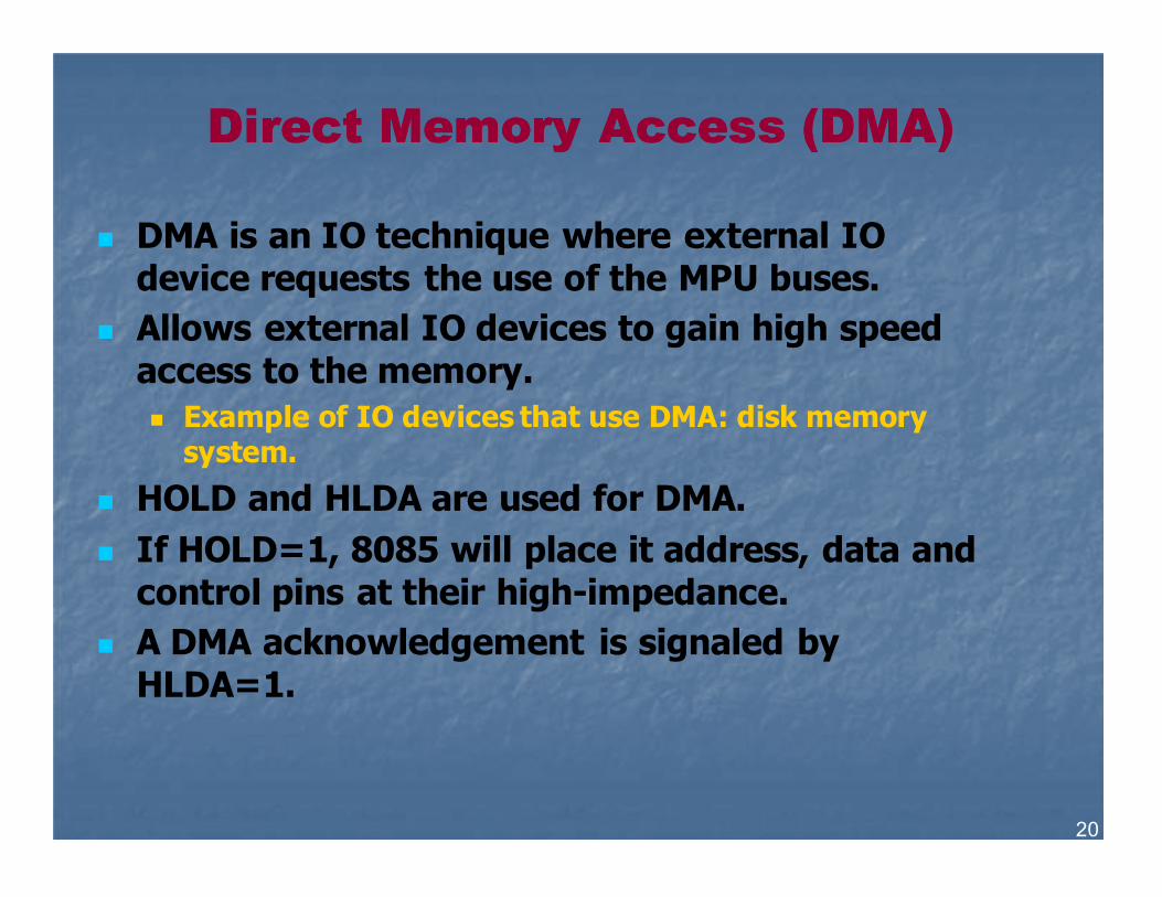
Direct Memory Access (DMA) Direct Memory Access (DMA)
� DMA is an IO technique where external IO device requests the use of the MPU buses.
� Allows external IO devices to gain high speed access to the memory.
� Example of IO devices that use DMA: disk memory system.
� HOLD and HLDA are used for DMA.
� If HOLD=1, 8085 will place it address, data and control pins at their high-impedance.
� A DMA acknowledgement is signaled by HLDA=1.
21
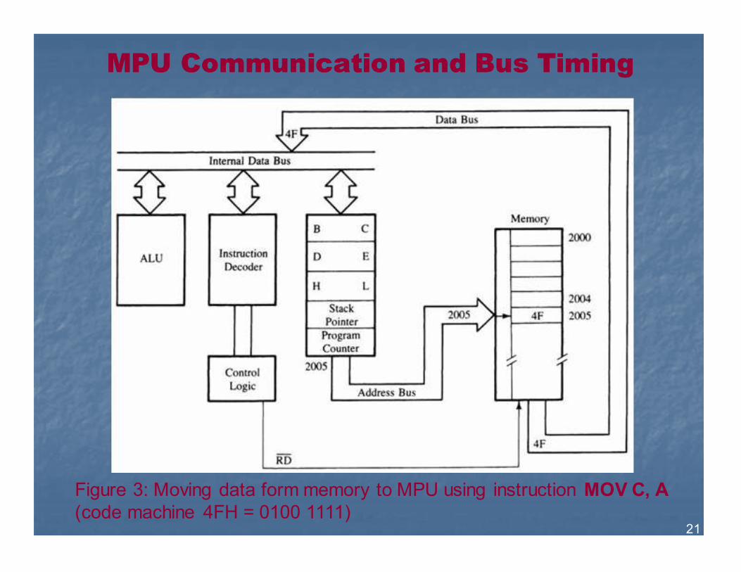
MPU Communication and Bus Timing MPU Communication and Bus Timing
Figure 3: Moving data form memory to MPU using instruction MOV C, A
(code machine 4FH = 0100 1111)
22
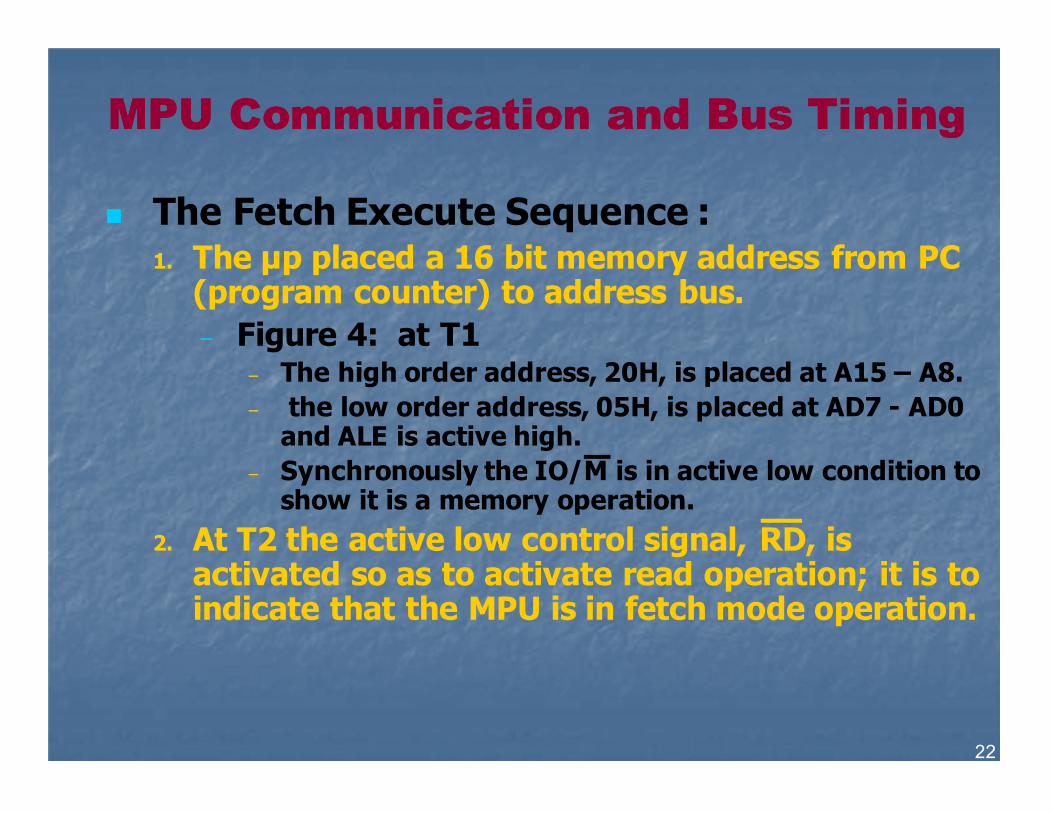
� The Fetch Execute Sequence : 1. The μp placed a 16 bit memory address from PC
(program counter) to address bus.
– Figure 4: at T1 – The high order address, 20H, is placed at A15 – A8.
– the low order address, 05H, is placed at AD7 - AD0 and ALE is active high.
– Synchronously the IO/M is in active low condition to show it is a memory operation.
2. At T2 the active low control signal, RD, is activated so as to activate read operation; it is to indicate that the MPU is in fetch mode operation.
MPU Communication and Bus Timing MPU Communication and Bus Timing
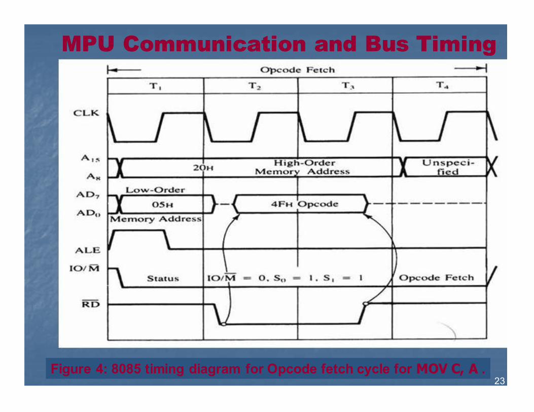
23 Figure 4: 8085 timing diagram for Opcode fetch cycle for MOV C, A .
MPU Communication and Bus Timing MPU Communication and Bus Timing
24
3. T3: The active low RD signal enabled the byte instruction, 4FH, to be placed on AD7 – AD0 and transferred to the MPU. While RD high, the data bus will be in high impedance mode.
4. T4: The machine code, 4FH, will then be decoded in instruction decoder. The content of accumulator (A) will then copied into C register at time state, T4.
MPU Communication and Bus Timing MPU Communication and Bus Timing

25
Thank you
Q&A