
Applications STD2NK100Z, STP2NK100Z, STU2NK100Z
23
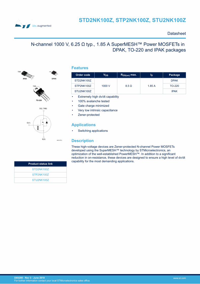
1 2 3 TAB TO-220 IPAK TAB 1 2 3 TAB 1 3 2 DPAK D(2, TAB) G(1) S(3) AM01475V1 Features Order code V DS R DS(on) max. I D Package STD2NK100Z 1000 V 8.5 Ω 1.85 A DPAK STP2NK100Z TO-220 STU2NK100Z IPAK • Extremely high dv/dt capability • 100% avalanche tested • Gate charge minimized • Very low intrinsic capacitance • Zener-protected Applications • Switching applications Description These high-voltage devices are Zener-protected N-channel Power MOSFETs developed using the SuperMESH™ technology by STMicroelectronics, an optimization of the well-established PowerMESH™. In addition to a significant reduction in on-resistance, these devices are designed to ensure a high level of dv/dt capability for the most demanding applications. Product status link STD2NK100Z STP2NK100Z STU2NK100Z N-channel 1000 V, 6.25 Ω typ., 1.85 A SuperMESH™ Power MOSFETs in DPAK, TO-220 and IPAK packages STD2NK100Z, STP2NK100Z, STU2NK100Z Datasheet DS5280 - Rev 3 - June 2018 For further information contact your local STMicroelectronics sales office. www.st.com
Transcript of Applications STD2NK100Z, STP2NK100Z, STU2NK100Z
12
3
TAB
TO-220
IPAK
TAB
12
3
TAB
132
DPAK
D(2, TAB)
G(1)
S(3)AM01475V1
FeaturesOrder code VDS RDS(on) max. ID Package
STD2NK100Z
1000 V 8.5 Ω 1.85 A
DPAK
STP2NK100Z TO-220
STU2NK100Z IPAK
• Extremely high dv/dt capability• 100% avalanche tested• Gate charge minimized• Very low intrinsic capacitance• Zener-protected
Applications• Switching applications
DescriptionThese high-voltage devices are Zener-protected N-channel Power MOSFETsdeveloped using the SuperMESH™ technology by STMicroelectronics, anoptimization of the well-established PowerMESH™. In addition to a significantreduction in on-resistance, these devices are designed to ensure a high level of dv/dtcapability for the most demanding applications.
Product status link
STD2NK100Z
STP2NK100Z
STU2NK100Z
N-channel 1000 V, 6.25 Ω typ., 1.85 A SuperMESH™ Power MOSFETs in DPAK, TO-220 and IPAK packages
STD2NK100Z, STP2NK100Z, STU2NK100Z
Datasheet
DS5280 - Rev 3 - June 2018For further information contact your local STMicroelectronics sales office.
www.st.com
1 Electrical ratings
Table 1. Absolute maximum ratings
Symbol Parameter Value Unit
VDS Drain-source voltage 1000 V
VGS Gate-source voltage ±30 V
ID Drain current (continuous) at TC = 25 °C 1.85 A
ID Drain current (continuous) at TC = 100 °C 1.16 A
IDM (1) Drain current (pulsed) 7.4 A
PTOT Total dissipation at TC = 25 °C 70 W
ESD Gate-source human body model (C = 100 pF, R =1.5 kΩ) 3 kV
dv/dt (2) Peak diode recovery voltage slope 2.5 V/ns
Tj Operating junction temperature range-55 to 150 °C
Tstg Storage temperature range
1. Pulse width limited by safe operating area.2. ISD ≤ 1.85 A, di/dt ≤ 200 A/µs, VDD = 80% V(BR)DSS.
Table 2. Thermal data
Symbol ParameterValue
UnitDPAK TO-220 IPAK
Rthj-case Thermal resistance junction-case 1.79
°C/WRthj-pcb (1) Thermal resistance junction-pcb 50 - -
Rthj-amb Thermal resistance junction-ambient 62.5 100
1. When mounted on FR-4 board of 1 inch², 2 oz Cu.
Table 3. Avalanche characteristics
Symbol Parameter Value Unit
IAR (1) Avalanche current, repetitive or not-repetitive 1.85 A
EAS (2). Single pulse avalanche energy 170 mJ
1. Pulse width limited by Tjmax.
2. Starting Tj = 25°C, ID = IAR, VDD = 50 V
STD2NK100Z, STP2NK100Z, STU2NK100ZElectrical ratings
DS5280 - Rev 3 page 2/23
2 Electrical characteristics
(TCASE = 25 °C unless otherwise specified)
Table 4. On/off states
Symbol Parameter Test conditions Min. Typ. Max. Unit
V(BR)DSSDrain-source breakdownvoltage VGS = 0 V, ID = 1 mA 1000 V
IDSSZero gate voltage draincurrent
VGS = 0 V, VDS = 1000 V 1 µA
VGS = 0 V, VDS = 1000 V,TC = 125 °C (1) 50 µA
IGSSGate-body leakagecurrent VDS = 0 V, VGS = ±30 V ±10 µA
VGS(th) Gate threshold voltage VDS = VGS, ID = 50 µA 3 3.75 4.5 V
RDS(on)Static drain-source onresistance VGS = 10 V, ID = 0.9 A 6.25 8.5 Ω
1. Defined by design, not subject to production test.
Table 5. Dynamic
Symbol Parameter Test conditions Min. Typ. Max. Unit
Ciss Input capacitanceVDS = 25 V, f = 1 MHz,
VGS = 0 V-
499
- pFCoss Output capacitance 53
CrssReverse transfercapacitance 9
Coss eq. (1) Equivalent outputcapacitance VGS = 0 V, VDS = 0 V to 800 V - 28 - pF
RG Gate input resistance f = 1 MHz, open drain - 6.6 - Ω
Qg Total gate charge VDD = 800 V, ID = 1.85 A,
VGS = 0 to 10 V
(see Figure 16. Test circuit for gate chargebehavior)
-
16
- nCQgs Gate-source charge 3
Qgd Gate-drain charge 9
1. Coss eq. is defined as a constant equivalent capacitance giving the same charging time as Coss when VDSincreases from 0 to80% VDSS.
Table 6. Switching times
Symbol Parameter Test conditions Min. Typ. Max. Unit
td(on) Turn-on delay time VDD = 500 V, ID = 0.9 A, RG = 4.7 Ω,VGS = 10 V
(see Figure 15. Test circuit for resistive loadswitching times and Figure 20. Switchingtime waveform)
-
7.2
- nstr Rise time 6.5
td(off) Turn-off delay time 41.5
tr Fall time 32.5
STD2NK100Z, STP2NK100Z, STU2NK100ZElectrical characteristics
DS5280 - Rev 3 page 3/23
Table 7. Source-drain diode
Symbol Parameter Test conditions Min. Typ. Max. Unit
ISD Source-drain current - 1.85A
ISDM (1) Source-drain current(pulsed) - 7.4
VSD (2) Forward on voltage ISD = 1.85 A, VGS = 0 V - 1.6 V
trr Reverse recovery time ISD = 1.85 A, di/dt = 100 A/µs
VDD = 60 V
(see Figure 17. Test circuit for inductiveload switching and diode recovery times)
- 476 ns
Qrr Reverse recovery charge - 1.6 μC
IRRM Reverse recovery current - 6.9 A
trr Reverse recovery time ISD = 1.85 A, di/dt = 100 A/µs
VDD = 60 V, Tj = 150 °C
(see Figure 17. Test circuit for inductiveload switching and diode recovery times)
- 532 ns
Qrr Reverse recovery charge - 1.9 μC
IRRM Reverse recovery current - 88 A
1. Pulse width is limited by safe operating area.2. Pulsed: pulse duration = 300 μs, duty cycle 1.5%.
Table 8. Gate-source Zener diode
Symbol Parameter Test conditions Min. Typ. Max. Unit
V(BR)GSOGate-source breakdownvoltage IGS = ±1 mA, ID = 0 A 30 - - V
The built-in back-to-back Zener diodes are specifically designed to enhance the ESD performance of the device.The Zener voltage facilitates efficient and cost-effective device integrity protection, thus eliminating the need foradditional external componentry.
STD2NK100Z, STP2NK100Z, STU2NK100ZElectrical characteristics
DS5280 - Rev 3 page 4/23
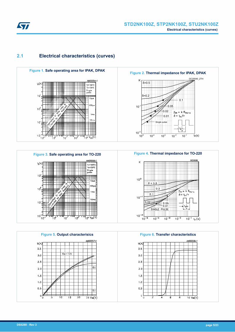
2.1 Electrical characteristics (curves)
Figure 1. Safe operating area for IPAK, DPAK Figure 2. Thermal impedance for IPAK, DPAK
δ=0.5K
10 tp(s)-5 10-4 10-3 10-110-2
δ=0.2
10-1
10-2
Single pulse
0.05
0.02
0.01
0.1
GC20540_ZTH
Figure 3. Safe operating area for TO-220 Figure 4. Thermal impedance for TO-220
Figure 5. Output characterisics Figure 6. Transfer characteristics
STD2NK100Z, STP2NK100Z, STU2NK100ZElectrical characteristics (curves)
DS5280 - Rev 3 page 5/23
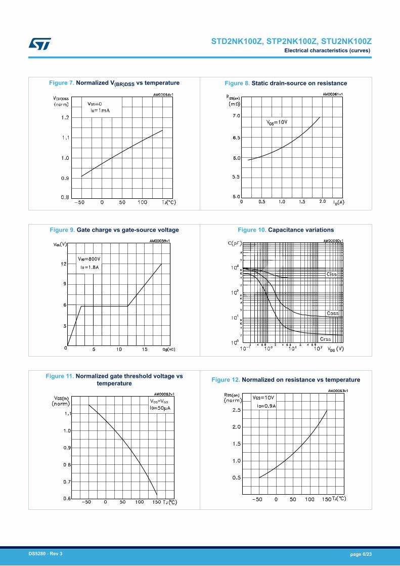
Figure 7. Normalized V(BR)DSS vs temperature Figure 8. Static drain-source on resistance
Figure 9. Gate charge vs gate-source voltage Figure 10. Capacitance variations
Figure 11. Normalized gate threshold voltage vstemperature
VDS=VGS
Figure 12. Normalized on resistance vs temperature
STD2NK100Z, STP2NK100Z, STU2NK100ZElectrical characteristics (curves)
DS5280 - Rev 3 page 6/23
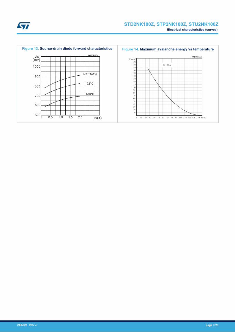
Figure 13. Source-drain diode forward characteristics Figure 14. Maximum avalanche energy vs temperature
TJ(°C)1401301201101009080706050403020100
EAS(mJ) 190 180 170 160 150 140 130 120 110 100 9080 70 60 50 4030 20 10
AM00056v1
ID=1.85A
STD2NK100Z, STP2NK100Z, STU2NK100ZElectrical characteristics (curves)
DS5280 - Rev 3 page 7/23
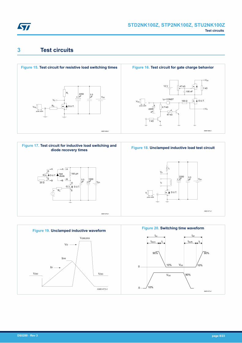
3 Test circuits
Figure 15. Test circuit for resistive load switching times
AM01468v1
VD
RG
RL
D.U.T.
2200μF VDD
3.3μF+
pulse width
VGS
Figure 16. Test circuit for gate charge behavior
AM01469v1
47 kΩ1 kΩ
47 kΩ
2.7 kΩ
1 kΩ
12 V
IG= CONST100 Ω
100 nF
D.U.T.
+pulse width
VGS
2200μF
VG
VDD
Figure 17. Test circuit for inductive load switching anddiode recovery times
AM01470v1
AD
D.U.T.S
B
G
25 Ω
A A
B B
RG
GD
S
100 µH
µF3.3 1000
µF VDD
D.U.T.
+
_
+
fastdiode
Figure 18. Unclamped inductive load test circuit
AM01471v1
VD
ID
D.U.T.
L
VDD+
pulse width
Vi
3.3µF
2200µF
Figure 19. Unclamped inductive waveform
AM01472v1
V(BR)DSS
VDDVDD
VD
IDM
ID
Figure 20. Switching time waveform
AM01473v1
0
VGS 90%
VDS
90%
10%
90%
10%
10%
ton
td(on) tr
0
toff
td(off) tf
STD2NK100Z, STP2NK100Z, STU2NK100ZTest circuits
DS5280 - Rev 3 page 8/23
4 Package information
In order to meet environmental requirements, ST offers these devices in different grades of ECOPACK®
packages, depending on their level of environmental compliance. ECOPACK® specifications, grade definitionsand product status are available at: www.st.com. ECOPACK® is an ST trademark.
STD2NK100Z, STP2NK100Z, STU2NK100ZPackage information
DS5280 - Rev 3 page 9/23
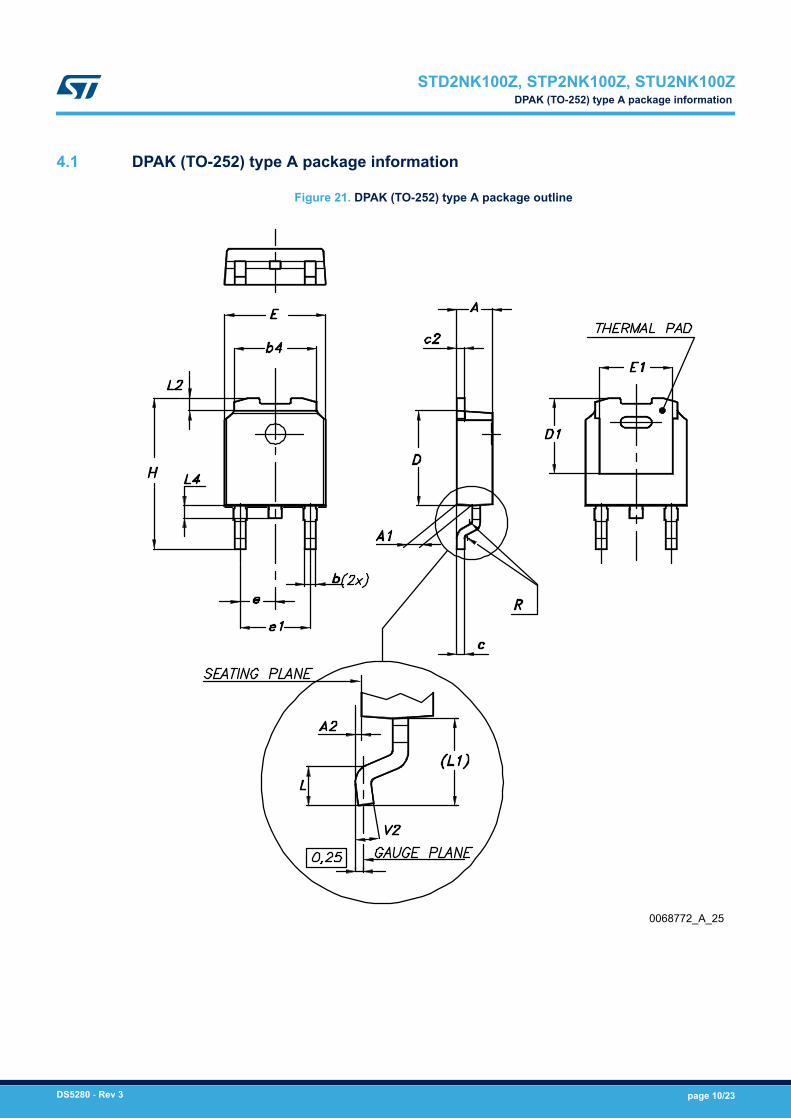
4.1 DPAK (TO-252) type A package information
Figure 21. DPAK (TO-252) type A package outline
0068772_A_25
STD2NK100Z, STP2NK100Z, STU2NK100ZDPAK (TO-252) type A package information
DS5280 - Rev 3 page 10/23
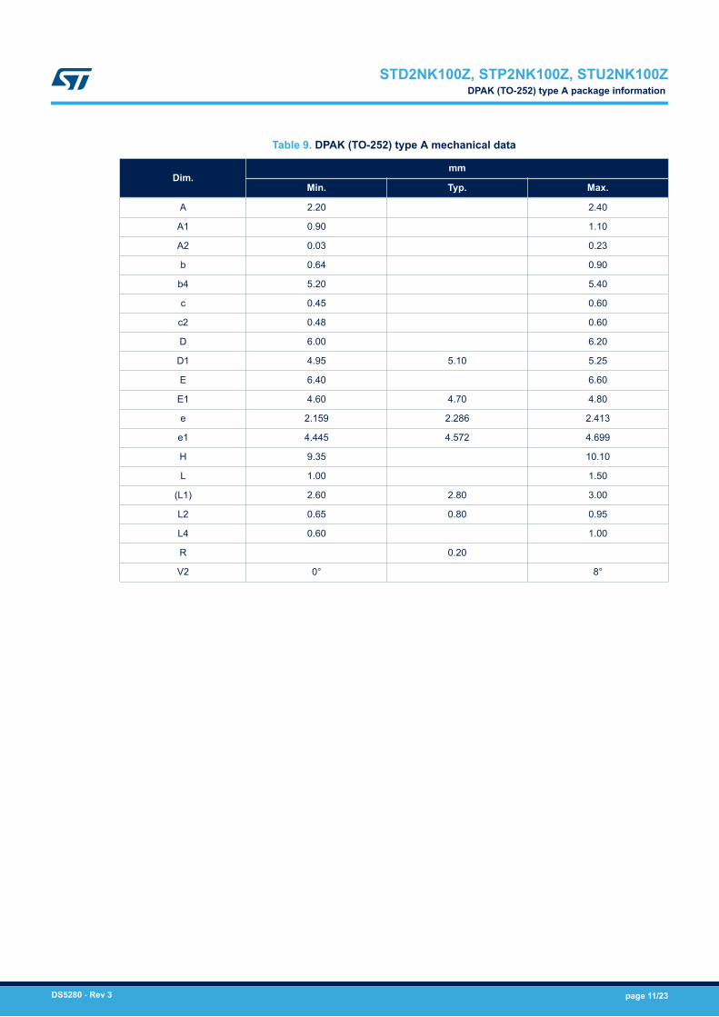
Table 9. DPAK (TO-252) type A mechanical data
Dim.mm
Min. Typ. Max.
A 2.20 2.40
A1 0.90 1.10
A2 0.03 0.23
b 0.64 0.90
b4 5.20 5.40
c 0.45 0.60
c2 0.48 0.60
D 6.00 6.20
D1 4.95 5.10 5.25
E 6.40 6.60
E1 4.60 4.70 4.80
e 2.159 2.286 2.413
e1 4.445 4.572 4.699
H 9.35 10.10
L 1.00 1.50
(L1) 2.60 2.80 3.00
L2 0.65 0.80 0.95
L4 0.60 1.00
R 0.20
V2 0° 8°
STD2NK100Z, STP2NK100Z, STU2NK100ZDPAK (TO-252) type A package information
DS5280 - Rev 3 page 11/23
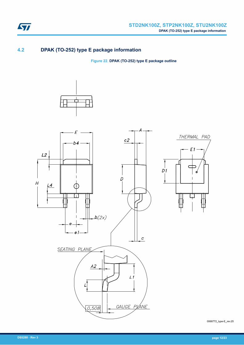
4.2 DPAK (TO-252) type E package information
Figure 22. DPAK (TO-252) type E package outline
0068772_type-E_rev.25
STD2NK100Z, STP2NK100Z, STU2NK100ZDPAK (TO-252) type E package information
DS5280 - Rev 3 page 12/23
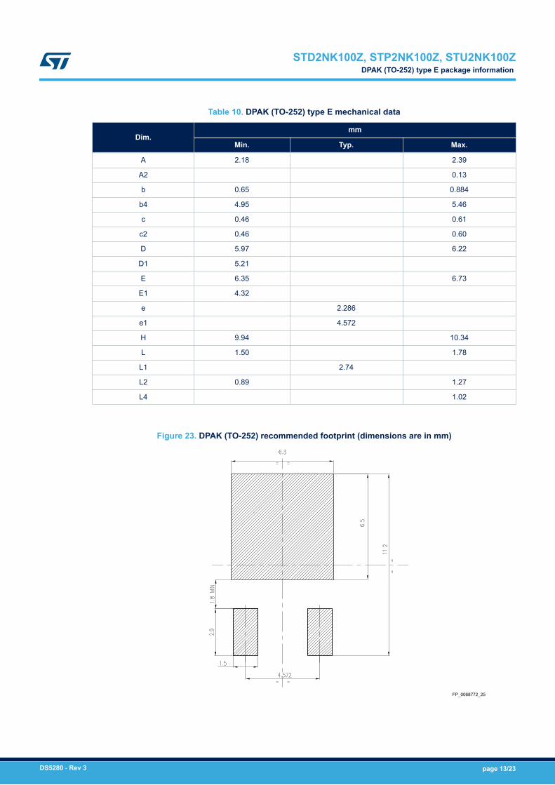
Table 10. DPAK (TO-252) type E mechanical data
Dim.mm
Min. Typ. Max.
A 2.18 2.39
A2 0.13
b 0.65 0.884
b4 4.95 5.46
c 0.46 0.61
c2 0.46 0.60
D 5.97 6.22
D1 5.21
E 6.35 6.73
E1 4.32
e 2.286
e1 4.572
H 9.94 10.34
L 1.50 1.78
L1 2.74
L2 0.89 1.27
L4 1.02
Figure 23. DPAK (TO-252) recommended footprint (dimensions are in mm)
FP_0068772_25
STD2NK100Z, STP2NK100Z, STU2NK100ZDPAK (TO-252) type E package information
DS5280 - Rev 3 page 13/23
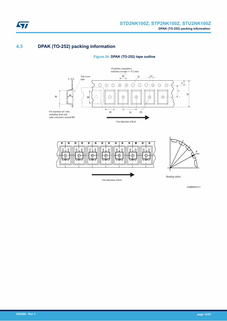
4.3 DPAK (TO-252) packing information
Figure 24. DPAK (TO-252) tape outline
P1A0 D1
P0
FW
E
D
B0K0
T
User direction of feed
P2
10 pitches cumulativetolerance on tape +/- 0.2 mm
User direction of feed
R
Bending radius
B1
For machine ref. onlyincluding draft andradii concentric around B0
AM08852v1
Top covertape
STD2NK100Z, STP2NK100Z, STU2NK100ZDPAK (TO-252) packing information
DS5280 - Rev 3 page 14/23
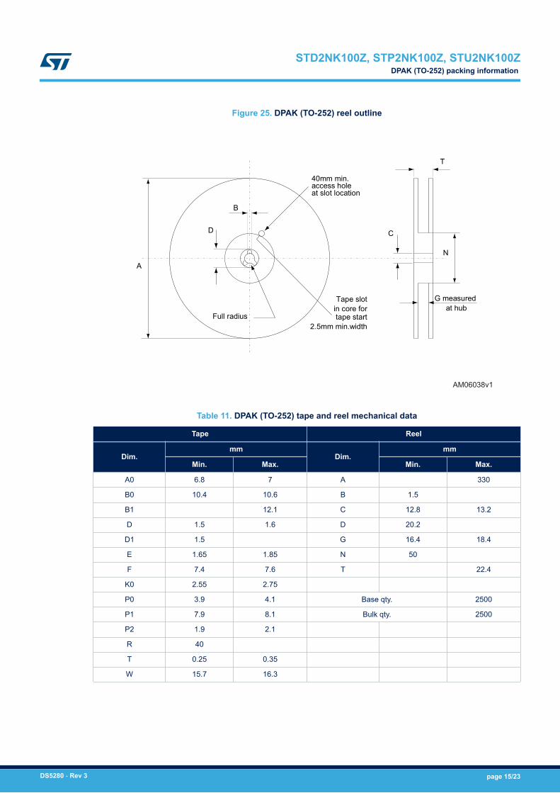
Figure 25. DPAK (TO-252) reel outline
A
D
B
Full radius
Tape slot in core for tape start
2.5mm min.width
G measured at hub
C
N
40mm min. access hole at slot location
T
AM06038v1
Table 11. DPAK (TO-252) tape and reel mechanical data
Tape Reel
Dim.mm
Dim.mm
Min. Max. Min. Max.
A0 6.8 7 A 330
B0 10.4 10.6 B 1.5
B1 12.1 C 12.8 13.2
D 1.5 1.6 D 20.2
D1 1.5 G 16.4 18.4
E 1.65 1.85 N 50
F 7.4 7.6 T 22.4
K0 2.55 2.75
P0 3.9 4.1 Base qty. 2500
P1 7.9 8.1 Bulk qty. 2500
P2 1.9 2.1
R 40
T 0.25 0.35
W 15.7 16.3
STD2NK100Z, STP2NK100Z, STU2NK100ZDPAK (TO-252) packing information
DS5280 - Rev 3 page 15/23
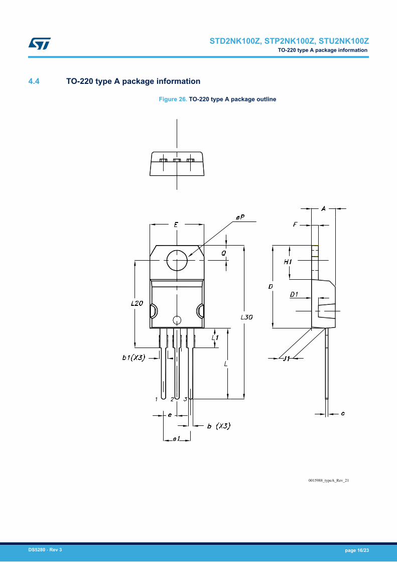
4.4 TO-220 type A package information
Figure 26. TO-220 type A package outline
0015988_typeA_Rev_21
STD2NK100Z, STP2NK100Z, STU2NK100ZTO-220 type A package information
DS5280 - Rev 3 page 16/23

Table 12. TO-220 type A package mechanical data
Dim.mm
Min. Typ. Max.
A 4.40 4.60
b 0.61 0.88
b1 1.14 1.55
c 0.48 0.70
D 15.25 15.75
D1 1.27
E 10.00 10.40
e 2.40 2.70
e1 4.95 5.15
F 1.23 1.32
H1 6.20 6.60
J1 2.40 2.72
L 13.00 14.00
L1 3.50 3.93
L20 16.40
L30 28.90
øP 3.75 3.85
Q 2.65 2.95
STD2NK100Z, STP2NK100Z, STU2NK100ZTO-220 type A package information
DS5280 - Rev 3 page 17/23
4.5 IPAK (TO-251) type A package information
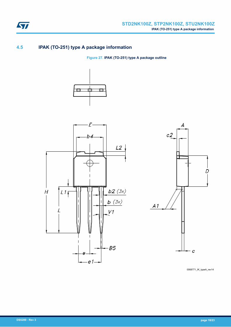
Figure 27. IPAK (TO-251) type A package outline
0068771_IK_typeA_rev14
STD2NK100Z, STP2NK100Z, STU2NK100ZIPAK (TO-251) type A package information
DS5280 - Rev 3 page 18/23
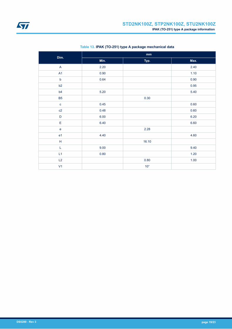
Table 13. IPAK (TO-251) type A package mechanical data
Dim.mm
Min. Typ. Max.
A 2.20 2.40
A1 0.90 1.10
b 0.64 0.90
b2 0.95
b4 5.20 5.40
B5 0.30
c 0.45 0.60
c2 0.48 0.60
D 6.00 6.20
E 6.40 6.60
e 2.28
e1 4.40 4.60
H 16.10
L 9.00 9.40
L1 0.80 1.20
L2 0.80 1.00
V1 10°
STD2NK100Z, STP2NK100Z, STU2NK100ZIPAK (TO-251) type A package information
DS5280 - Rev 3 page 19/23
5 Ordering information
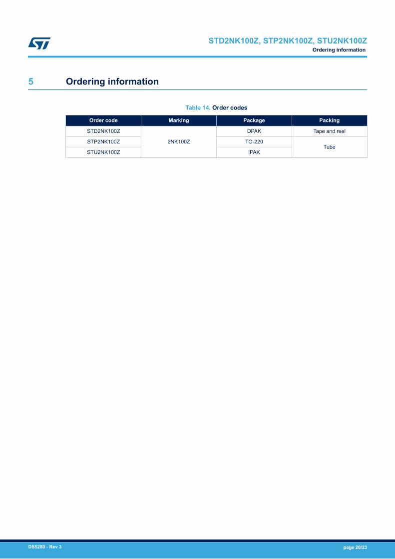
Table 14. Order codes
Order code Marking Package Packing
STD2NK100Z
2NK100Z
DPAK Tape and reel
STP2NK100Z TO-220Tube
STU2NK100Z IPAK
STD2NK100Z, STP2NK100Z, STU2NK100ZOrdering information
DS5280 - Rev 3 page 20/23
Revision history
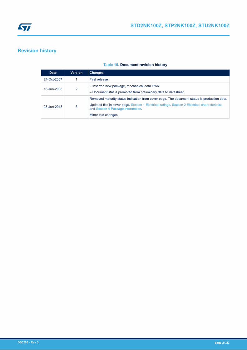
Table 15. Document revision history
Date Version Changes
24-Oct-2007 1 First release
18-Jun-2008 2– Inserted new package, mechanical data IPAK
– Document status promoted from preliminary data to datasheet.
28-Jun-2018 3
Removed maturity status indication from cover page. The document status is production data.
Updated title in cover page, Section 1 Electrical ratings, Section 2 Electrical characteristicsand Section 4 Package information.
Minor text changes.
STD2NK100Z, STP2NK100Z, STU2NK100Z
DS5280 - Rev 3 page 21/23
Contents
1 Electrical ratings . . . . . . . . . . . . . . . . . . . . . . . . . . . . . . . . . . . . . . . . . . . . . . . . . . . . . . . . . . . . . . . . . .2
2 Electrical characteristics. . . . . . . . . . . . . . . . . . . . . . . . . . . . . . . . . . . . . . . . . . . . . . . . . . . . . . . . . . .3
2.1 Electrical characteristics (curves) . . . . . . . . . . . . . . . . . . . . . . . . . . . . . . . . . . . . . . . . . . . . . . . . . 5
3 Test circuits . . . . . . . . . . . . . . . . . . . . . . . . . . . . . . . . . . . . . . . . . . . . . . . . . . . . . . . . . . . . . . . . . . . . . . .8
4 Package information. . . . . . . . . . . . . . . . . . . . . . . . . . . . . . . . . . . . . . . . . . . . . . . . . . . . . . . . . . . . . . .9
4.1 DPAK (TO-252) type A package information . . . . . . . . . . . . . . . . . . . . . . . . . . . . . . . . . . . . . . . . 9
4.2 DPAK (TO-252) type E package information . . . . . . . . . . . . . . . . . . . . . . . . . . . . . . . . . . . . . . . 11
4.3 DPAK (TO-252) packing information. . . . . . . . . . . . . . . . . . . . . . . . . . . . . . . . . . . . . . . . . . . . . . 13
4.4 TO-220 type A package information . . . . . . . . . . . . . . . . . . . . . . . . . . . . . . . . . . . . . . . . . . . . . . 15
4.5 IPAK (TO-251) type A package information . . . . . . . . . . . . . . . . . . . . . . . . . . . . . . . . . . . . . . . . 17
5 Ordering information . . . . . . . . . . . . . . . . . . . . . . . . . . . . . . . . . . . . . . . . . . . . . . . . . . . . . . . . . . . . .20
Revision history . . . . . . . . . . . . . . . . . . . . . . . . . . . . . . . . . . . . . . . . . . . . . . . . . . . . . . . . . . . . . . . . . . . . . . .21
STD2NK100Z, STP2NK100Z, STU2NK100ZContents
DS5280 - Rev 3 page 22/23
IMPORTANT NOTICE – PLEASE READ CAREFULLY
STMicroelectronics NV and its subsidiaries (“ST”) reserve the right to make changes, corrections, enhancements, modifications, and improvements to STproducts and/or to this document at any time without notice. Purchasers should obtain the latest relevant information on ST products before placing orders. STproducts are sold pursuant to ST’s terms and conditions of sale in place at the time of order acknowledgement.
Purchasers are solely responsible for the choice, selection, and use of ST products and ST assumes no liability for application assistance or the design ofPurchasers’ products.
No license, express or implied, to any intellectual property right is granted by ST herein.
Resale of ST products with provisions different from the information set forth herein shall void any warranty granted by ST for such product.
ST and the ST logo are trademarks of ST. All other product or service names are the property of their respective owners.
Information in this document supersedes and replaces information previously supplied in any prior versions of this document.
© 2018 STMicroelectronics – All rights reserved
STD2NK100Z, STP2NK100Z, STU2NK100Z
DS5280 - Rev 3 page 23/23