AN-2010LM3423 Buck-Boost2 Layer Evaluation Board · 4 C6(a-d) 10 µF X7R 10% 50V ... 1 R9 0.2Ω1%...
17
V IN (V) EFFICIENCY (%) 100 95 90 85 80 75 70 0 16 32 48 64 80 Q1 is IPD200N15N3 Q1 is FDD3682 User's Guide SNVA415C – June 2010 – Revised May 2013 AN-2010 LM3423 Buck-Boost 2 Layer Evaluation Board 1 Introduction This wide range evaluation board showcases the LM3423 NFET controller used with a buck-boost current regulator. It is designed to drive 4 to 8 LEDs at a maximum average LED current of 700mA from a DC input voltage of 10 to 70V. The evaluation board showcases most features of the LM3423 including PWM dimming, fault and LED status flags, output overvoltage protection and input under-voltage lockout. Note that there are two revisions of this PCB. The documentation for the latest revision (551600305-002 RevA) is shown first. The schematic, layout and bill of materials for the first revision (551600305-001 Rev1) can be found at the end of this document. The buck-boost circuit can be easily redesigned for different specifications by changing only a few components (see the Alternate Designs section found at the end of this application note). Note that design modifications can change the system efficiency. See the LM3421/21Q1/21Q0 LM3423/23Q1/23Q0 N-Ch Controllers for Constant Current LED Drivers (SNVS574) data sheet for a comprehensive explanation of the device and application information. Figure 1. Efficiency with 6 Series LEDS at 700mA All trademarks are the property of their respective owners. 1 SNVA415C – June 2010 – Revised May 2013 AN-2010 LM3423 Buck-Boost 2 Layer Evaluation Board Submit Documentation Feedback Copyright © 2010–2013, Texas Instruments Incorporated
Transcript of AN-2010LM3423 Buck-Boost2 Layer Evaluation Board · 4 C6(a-d) 10 µF X7R 10% 50V ... 1 R9 0.2Ω1%...
VIN (V)
EF
FIC
IEN
CY
(%
)
100
95
90
85
80
75
700 16 32 48 64 80
Q1 is IPD200N15N3
Q1 is FDD3682
User's GuideSNVA415C–June 2010–Revised May 2013
AN-2010 LM3423 Buck-Boost 2 Layer Evaluation Board
1 Introduction
This wide range evaluation board showcases the LM3423 NFET controller used with a buck-boost currentregulator. It is designed to drive 4 to 8 LEDs at a maximum average LED current of 700mA from a DCinput voltage of 10 to 70V.
The evaluation board showcases most features of the LM3423 including PWM dimming, fault and LEDstatus flags, output overvoltage protection and input under-voltage lockout. Note that there are tworevisions of this PCB. The documentation for the latest revision (551600305-002 RevA) is shown first. Theschematic, layout and bill of materials for the first revision (551600305-001 Rev1) can be found at the endof this document.
The buck-boost circuit can be easily redesigned for different specifications by changing only a fewcomponents (see the Alternate Designs section found at the end of this application note). Note that designmodifications can change the system efficiency. See the LM3421/21Q1/21Q0 LM3423/23Q1/23Q0 N-ChControllers for Constant Current LED Drivers (SNVS574) data sheet for a comprehensive explanation ofthe device and application information.
Figure 1. Efficiency with 6 Series LEDS at 700mA
All trademarks are the property of their respective owners.
1SNVA415C–June 2010–Revised May 2013 AN-2010 LM3423 Buck-Boost 2 Layer Evaluation BoardSubmit Documentation Feedback
Copyright © 2010–2013, Texas Instruments Incorporated
C4,
C6(a-d)
Q1
R18
R11
R9
R20
C12
C11
Q5
VIN
Q7
Q6Q4
D2
DIM
R17
R19
DIM Q2
VIN
L1
C9
R6
C8
R1
R10
R13
R5
R8
R7
R4
C7
C2, C3
OVP
nDIM
LM3423
AGND
PGND
DDRV
DAP
GATE
EN
COMP
VIN
CSH
RCT
IS
HSP
RPD
VCC
HSN1
2
3
4
5
6
7
8
20
19
18
17
16
15
14
13
FLT DPOL9 12
TIMR LRDY10 11
R2
C10
R14
VIN
R15
VIN
VCC
VCC
LED-
D1TP1
Q3 PWM
R12
TP5
RPD
RPD
TP10
GND
J3C1
R3J1
J2J5
LED+J4
TP6GND
Schematic for 551600305-002 REVA www.ti.com
2 Schematic for 551600305-002 REVA
Figure 2. Board Schematic
2 AN-2010 LM3423 Buck-Boost 2 Layer Evaluation Board SNVA415C–June 2010–Revised May 2013Submit Documentation Feedback
Copyright © 2010–2013, Texas Instruments Incorporated
www.ti.com Pin Descriptions
3 Pin Descriptions
LM3423 LM3421 Name Description Function
Bypass with 100 nF capacitor to AGND as close to1 1 VIN Input Voltage the device as possible in the circuit board layout.
Connect to AGND for zero current shutdown or2 2 EN Enable apply > 2.4V to enable device.
Connect a capacitor to AGND to set the3 3 COMP Compensation compensation.
Connect a resistor to AGND to set the signal current.For analog dimming, connect a controlled current4 4 CSH Current Sense High source or a potentiometer to AGND as detailed inthe Analog Dimming section.
External RC network sets the predictive “off-time”5 5 RCT Resistor Capacitor Timing and thus the switching frequency.
Connect to PGND through the DAP copper pad to6 6 AGND Analog Ground provide ground return for CSH, COMP, RCT, and
TIMR.
Connect to a resistor divider from VO to programoutput over-voltage lockout (OVLO). Turn-off7 7 OVP Over-Voltage Protection threshold is 1.24V and hysteresis for turn-on isprovided by 23 µA current source.
Connect a PWM signal for dimming as detailed inthe PWM Dimming section and/or a resistor dividerDimming Input /8 8 nDIM from VIN to program input under-voltage lockoutUnder-Voltage Protection (UVLO). Turn-on threshold is 1.24V and hysteresisfor turn-off is provided by 23 µA current source.
Connect to pull-up resistor from VIN and N-channel9 - FLT Fault Flag MosFET open drain output is high when a fault
condition is latched by the timer.
Connect a capacitor to AGND to set the time delay10 - TIMR Fault Timer before a sensed fault condition is latched.
Connect to pull-up resistor from VIN and N-channel11 - LRDY LED Ready Flag MosFET open drain output pulls down when the
LED current is not in regulation.
Connect to AGND if dimming with a series P-12 - DPOL Dim Polarity channel MosFET or leave open when dimming with
series N-channel MosFET.
13 9 DDRV Dim Gate Drive Output Connect to the gate of the dimming MosFET.
Connect to AGND through the DAP copper pad to14 10 PGND Power Ground provide ground return for GATE and DDRV.
15 11 GATE Main Gate Drive Output Connect to the gate of the main switching MosFET.
Bypass with 2.2 µF–3.3 µF ceramic capacitor to16 12 VCC Internal Regulator Output PGND.
Connect to the drain of the main N-channel MosFET17 13 IS Main Switch Current Sense switch for RDS-ON sensing or to a sense resistor
installed in the source of the same device.
Connect the low side of all external resistor dividers18 14 RPD Resistor Pull Down (VIN UVLO, OVP) to implement “zero-current”
shutdown.
Connect through a series resistor to the positive side19 15 HSP LED Current Sense Positive of the LED current sense resistor.
Connect through a series resistor to the negative20 16 HSN LED Current Sense Negative side of the LED current sense resistor.
DAP (21) DAP (17) DAP Thermal PAD on bottom of IC Star ground, connecting AGND and PGND.
3SNVA415C–June 2010–Revised May 2013 AN-2010 LM3423 Buck-Boost 2 Layer Evaluation BoardSubmit Documentation Feedback
Copyright © 2010–2013, Texas Instruments Incorporated
Bill of Materials for 551600305-002 REVA www.ti.com
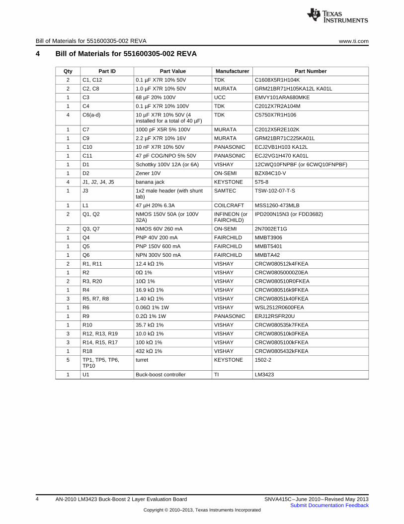
4 Bill of Materials for 551600305-002 REVA
Qty Part ID Part Value Manufacturer Part Number
2 C1, C12 0.1 µF X7R 10% 50V TDK C1608X5R1H104K
2 C2, C8 1.0 µF X7R 10% 50V MURATA GRM21BR71H105KA12L KA01L
1 C3 68 µF 20% 100V UCC EMVY101ARA680MKE
1 C4 0.1 µF X7R 10% 100V TDK C2012X7R2A104M
4 C6(a-d) 10 µF X7R 10% 50V (4 TDK C5750X7R1H106installed for a total of 40 µF)
1 C7 1000 pF X5R 5% 100V MURATA C2012X5R2E102K
1 C9 2.2 µF X7R 10% 16V MURATA GRM21BR71C225KA01L
1 C10 10 nF X7R 10% 50V PANASONIC ECJ2VB1H103 KA12L
1 C11 47 pF COG/NPO 5% 50V PANASONIC ECJ2VG1H470 KA01L
1 D1 Schottky 100V 12A (or 6A) VISHAY 12CWQ10FNPBF (or 6CWQ10FNPBF)
1 D2 Zener 10V ON-SEMI BZX84C10-V
4 J1, J2, J4, J5 banana jack KEYSTONE 575-8
1 J3 1x2 male header (with shunt SAMTEC TSW-102-07-T-Stab)
1 L1 47 µH 20% 6.3A COILCRAFT MSS1260-473MLB
2 Q1, Q2 NMOS 150V 50A (or 100V INFINEON (or IPD200N15N3 (or FDD3682)32A) FAIRCHILD)
2 Q3, Q7 NMOS 60V 260 mA ON-SEMI 2N7002ET1G
1 Q4 PNP 40V 200 mA FAIRCHILD MMBT3906
1 Q5 PNP 150V 600 mA FAIRCHILD MMBT5401
1 Q6 NPN 300V 500 mA FAIRCHILD MMBTA42
2 R1, R11 12.4 kΩ 1% VISHAY CRCW080512k4FKEA
1 R2 0Ω 1% VISHAY CRCW08050000Z0EA
2 R3, R20 10Ω 1% VISHAY CRCW080510R0FKEA
1 R4 16.9 kΩ 1% VISHAY CRCW080516k9FKEA
3 R5, R7, R8 1.40 kΩ 1% VISHAY CRCW08051k40FKEA
1 R6 0.06Ω 1% 1W VISHAY WSL2512R0600FEA
1 R9 0.2Ω 1% 1W PANASONIC ERJ12RSFR20U
1 R10 35.7 kΩ 1% VISHAY CRCW080535k7FKEA
3 R12, R13, R19 10.0 kΩ 1% VISHAY CRCW080510k0FKEA
3 R14, R15, R17 100 kΩ 1% VISHAY CRCW0805100kFKEA
1 R18 432 kΩ 1% VISHAY CRCW0805432kFKEA
5 TP1, TP5, TP6, turret KEYSTONE 1502-2TP10
1 U1 Buck-boost controller TI LM3423
4 AN-2010 LM3423 Buck-Boost 2 Layer Evaluation Board SNVA415C–June 2010–Revised May 2013Submit Documentation Feedback
Copyright © 2010–2013, Texas Instruments Incorporated
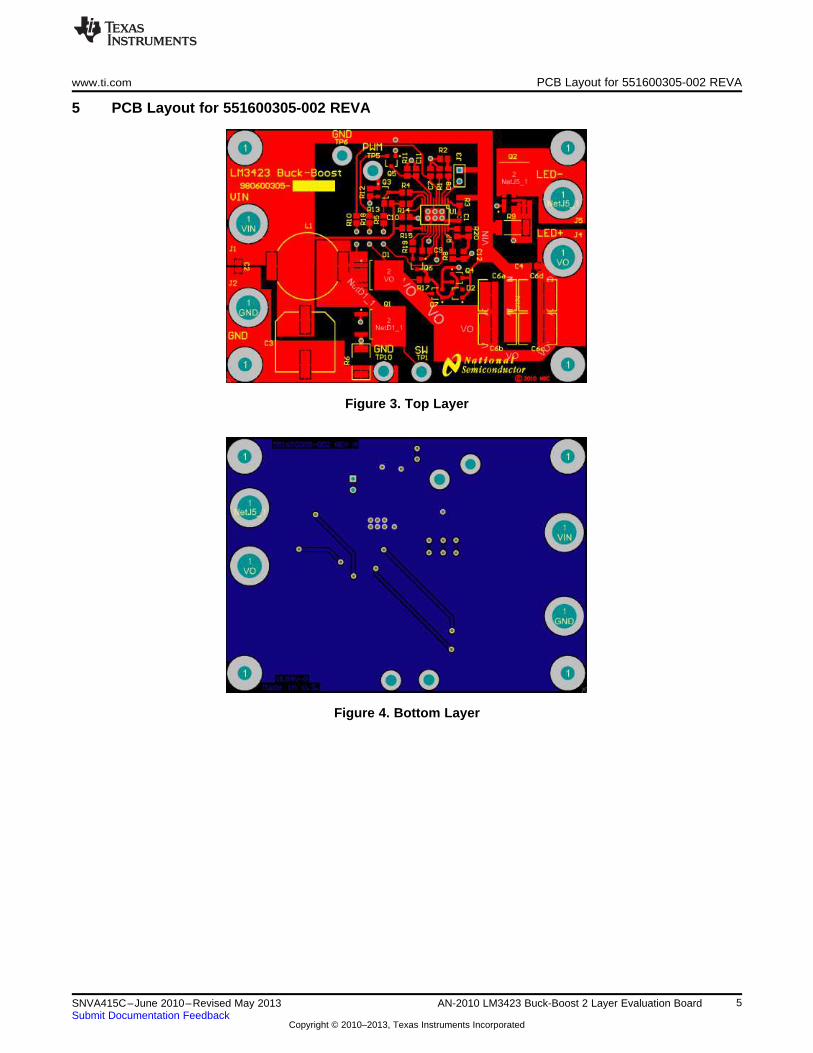
www.ti.com PCB Layout for 551600305-002 REVA
5 PCB Layout for 551600305-002 REVA
Figure 3. Top Layer
Figure 4. Bottom Layer
5SNVA415C–June 2010–Revised May 2013 AN-2010 LM3423 Buck-Boost 2 Layer Evaluation BoardSubmit Documentation Feedback
Copyright © 2010–2013, Texas Instruments Incorporated
2525=
35.7 k: x 1 nFfSW =
R10 x C7= 700 kHz
2525=
700 kHz x 1 nF= 35.7 k:R10 =
fSW x C7
21V=
21V + 10V= 0.677DMAX = VO + VIN-MIN
VO
21V=
21V + 70V= 0.231DMIN =
VO + VIN-MAX
VO
D' = 1 - D = 1 - 0.467 = 0.533
D = =21V
VO + VIN 21V + 24V= 0.467
VO
rD = N x rLED = 6 x 325 m: = 1.95:
VO = N x VLED = 6 x 3.5V = 21V
Design Procedure www.ti.com
6 Design Procedure
Refer to the LM3421/21Q1/21Q0 LM3423/23Q1/23Q0 N-Ch Controllers for Constant Current LED Drivers(SNVS574 data sheet for design considerations.
6.1 Specifications
N = 6
VLED = 3.5V
rLED = 325 mΩ
VIN = 24V
VIN-MIN = 10V; VIN-MAX = 70V
fSW = 700 kHz
VSNS = 150 mV
ILED = 700 mA
ΔiL-PP = 350 mA
ΔiLED-PP = 50 mA
ΔvIN-PP = 100 mV
ILIM = 4A
VTURN-ON = 10V; VHYS = 3.4V
VTURN-OFF =44V; VHYSO = 10V
6.2 Operating Point
Solve for VO and rD:
(1)
(2)
Solve for D, D', DMAX, and DMIN:
(3)
(4)
(5)
(6)
6.3 Switching Frequency
Assume C7 = 1 nF and solve for R10:
(7)
The closest standard resistor is actually 35.7 kΩ therefore the fSW is:
(8)
6 AN-2010 LM3423 Buck-Boost 2 Layer Evaluation Board SNVA415C–June 2010–Revised May 2013Submit Documentation Feedback
Copyright © 2010–2013, Texas Instruments Incorporated
700 mA x 0.4671.95: x 50 mA x 700 kHz
= 4.79 PFCO =
CO =rD x 'iLED-PP x fSW
ILED x D
L1 = 47 PH
340 mA x 0.533700 mA
IL-RMS =ILED
D'
IL-RMS =700 mA0.533
IL-RMS = 1.32A
ILED
'IL-PP x D'2
¸¸¹
·¨¨©
§
¸¸¹
·¨¨©
§
1 +121
x
1 +121
x
2
x
x
24V x 0.467=
47 PH x 700 kHz= 340 mA'iL-PP =
L1 x fSW
VIN x D
24V x 0.467=
350 mA x 700 kHz= 46 PHL1 =
'iL-PP x fSW
VIN x D
R8 = R7 = 1.4 k:
R1 = 12.4 k:
R9 = 0.2:
1.24V x 1.4 k:= = 700 mAILED =
1.24V x R8R9 x R1 0.2: x 12.4 k:
30107716
700 mA x 12.4 k: x 0.2:=
1.24V= 1.4 k:R8 =
ILED x R1 x R91.24V
30107715
150 mV=700 mA
= 0.214:R9 =VSNS
ILED
C7 = 1 nF R10 = 35.7 k:
www.ti.com Design Procedure
The chosen components from Section 6.3 are:
(9)
6.4 Average LED Current
Solve for R9:
(10)
Assume R1 = 12.4 kΩ and solve for R8:
(11)
The closest standard resistor for R9 is 0.2Ω and the closest for R8 (and R7) is actually 1.4 kΩ thereforeILED is:
(12)
The chosen components from Section 6.4 are:
(13)
6.5 Inductor Ripple Current
Solve for L1:
(14)
The closest standard inductor is 47 µH therefore the actual ΔiL-PP is:
(15)
Determine minimum allowable RMS current rating:
(16)
The chosen component from Section 6.5 is:
(17)
6.6 Output Capacitance
Solve for CO:
(18)
7SNVA415C–June 2010–Revised May 2013 AN-2010 LM3423 Buck-Boost 2 Layer Evaluation BoardSubmit Documentation Feedback
Copyright © 2010–2013, Texas Instruments Incorporated
radsecZP3 = 25k x 10 = 250k
ZP3 = max (ZP1, ZZ1) x 10 = ZZ1 x 10
radsec
= = 0.28 PFC8 =1
radsec
ZP2 x 5e6:
1
0.709 x 5e6:
ZP1=
5 x 5360= 0.709ZP2 =
5 x TU0
min(ZP1, ZZ1) radsec=
5 x 5360
19kradsec
0.533 x 620V=
1.467 x 700 mA x 0.06:= 5360TU0 =
(1 + D) x ILED x R6D' x 620V
1.95: x 0.5332
=0.467 x 47 PH
= 25kZZ1 =D x L1rD x D'2 rad
sec
1.467=
1.95: x 40 PF= 19kZP1 =
rD x CO
1 + D radsec
R6 = 0.06:
=0.06:
= 4.1AILIM =R6
245 mV 245 mV
=4A
= 0.061:R6 =ILIM
245 mV 245 mV
C6 = 4 x 10 PF
1- 0.677= 1.01A
1 - DMAX
DMAXICO-RMS = ILED x = 700 mA x 0.677
700 mA x 0.4671.95: x 40 PF x 700 kHz
= 6 mA'iLED-PP =
rD x CO x fSW
ILED x D'iLED-PP =
Design Procedure www.ti.com
A total value of 40 µF (using 4 10 µF X7R ceramic capacitors) is chosen therefore the actual ΔiLED-PP is:
(19)
Determine minimum allowable RMS current rating:
(20)
The chosen components from Section 6.6 are:
(21)
6.7 Peak Current lmit
Solve for R6:
(22)
The closest standard resistor is 0.06 Ω therefore ILIM is:
(23)
The chosen component from Section 6.7 is:
(24)
6.8 Loop Compensation
ωP1 is approximated:
(25)
ωZ1 is approximated:
(26)
TU0 is approximated:
(27)
To ensure stability, calculate ωP2:
(28)
Solve for C8:
(29)
To attenuate switching noise, calculate ωP3:
(30)
8 AN-2010 LM3423 Buck-Boost 2 Layer Evaluation Board SNVA415C–June 2010–Revised May 2013Submit Documentation Feedback
Copyright © 2010–2013, Texas Instruments Incorporated
PD = ID x VFD = 700 mA x 600 mV = 420 mW
ID-MAX = ILED = 700 mA
VRD-MAX = VIN-MAX + VO = 70V + 21V = 91V
Q1 o 40A, 100V, DPAK
PT = IT-RMS2 x RDSON = 897 mA2 x 50 m: = 40 mW
x x700 mAD =
0.533IT-RMS =
ILED
D'0.467 = 897 mA
0.6771 - 0.677
x 700 mA = 1.46AIT-MAX =
VT-MAX = VIN-MAX + VO = 70V + 21V = 91V
C3 = 68 PF
1- 0.677= 1.01A
1 - DMAX
DMAXICO-RMS = ILED x = 700 mA x
0.677
700 mA x 0.467=
100 mV x 700 kHz= 4.67 PFCIN =
'VIN-PP x fSW
ILED x D
C8 = 1.0 PFR20 = 10:C12 = 0.1 PF
= = 0.4 PFC12 =1
radsec
1
10: x 250k10: x ZP3
www.ti.com Design Procedure
Assume R20 = 10Ω and solve for C12:
(31)
Since PWM dimming can be evaluated with this board, a much larger compensation capacitor C8 = 1.0 µFis chosen and a smaller high frequency capacitor C12 = 0.1 µF is chosen.
The chosen components from Section 6.8 are:
(32)
6.9 Input Capacitance
Solve for the minimum CIN:
(33)
To minimize power supply interaction a much larger capacitance of 68 µF is used, therefore the actualΔvIN-PP is much lower.
Determine minimum allowable RMS current rating:
(34)
The chosen components from Section 6.9 are:
(35)
6.10 NFET
Determine minimum Q1 voltage rating and current rating:
(36)
(37)
A 100V NFET is chosen with a current rating of 40A due to the low RDS-ON = 50 mΩ. Determine IT-RMS andPT:
(38)
(39)
The chosen component from Section 6.10 is:
(40)
6.11 DIODE
Determine minimum D1 voltage rating and current rating:
(41)
(42)
A 100V diode is chosen with a current rating of 12A and VD = 600 mV. Determine PD:
(43)
9SNVA415C–June 2010–Revised May 2013 AN-2010 LM3423 Buck-Boost 2 Layer Evaluation BoardSubmit Documentation Feedback
Copyright © 2010–2013, Texas Instruments Incorporated
VTURN-OFF =R11
1.24V x (0.5 x 12.4 k: + 432 k:)12.4 k:
1.24V x (R11 + R18)
= 44VVTURN-OFF =
1.24V x R18VTURN-OFF ± 620 mV
= 12.3 k:R11 = =1.24V x 432 k:44V ± 620 mV
VHYSO = R18 x 23 PA = 432 k: x 23 PA = 9.9V
VHYSO
23 PA= 435 k:R18 =
10V=
23 PA
R4 = 16.9 k:
R13 = 10 k:
R5 = 1.4 k:
VHYS =R5
23 PA x 16.9 k: x (1.4 k: + 10 k:)1.4 k:
VHYS =
+ 23 PA x R1323 PA x R4 x (R5 + R13)
+ 23 PA x 10 k: = 3.4V
R4 =R5 x (VHYS - 23 PA x R13)
23 PA x (R5 + R13)
= 16.9 k:R4 =1.4 k: x (3.4V - 23 PA x 10 k:)
23 PA x (1.4 k: + 10 k:)
VTURN-ON =R5
1.24V x (1.4 k: + 10 k:)1.4 k:
1.24V x (R5 + R13)
= 10.1VVTURN-ON =
1.24V x R13VTURN-ON - 1.24V
= 1.42 k:R5 = =1.24V x 10 k:10V - 1.24V
D1 o 12A, 100V, DPAK
Design Procedure www.ti.com
The chosen component from Section 6.11 is:
(44)
6.12 Input UVLO
Since PWM dimming will be evaluated, a three resistor network will be used. Assume R13 = 10 kΩ andsolve for R5:
(45)
The closest standard resistor is 1.4 kΩ therefore VTURN-ON is:
(46)
Solve for R4:
(47)
The closest standard resistor is 16.9 kΩ making VHYS:
(48)
The chosen components from Section 6.12 are:
(49)
6.13 Output OVLO
Solve for R18:
(50)
The closest standard resistor is 432 kΩ therefore VHYSO is:
(51)
Solve for R11:
(52)
The closest standard resistor is 12.4 kΩ making VTURN-OFF:
(53)
10 AN-2010 LM3423 Buck-Boost 2 Layer Evaluation Board SNVA415C–June 2010–Revised May 2013Submit Documentation Feedback
Copyright © 2010–2013, Texas Instruments Incorporated
R11 = 12.4 k:R18 = 432 k:
www.ti.com Design Procedure
The chosen components from Section 6.13 are:
(54)
6.14 PWM Dimming
The LM3423 Buck-boost Evaluation board is configured to demonstrate PWM dimming of the LEDs. Forbest operation, use a PWM signal that has greater than 3V amplitude at a frequency between 120Hz and5kHz. Apply the PWM signal to the BNC connector (J6) and the inverted signal (seen by the nDIM pin)can be monitored at TP5.
The output PWM drive signal (DDRV) is level shifted to the floating LED stack using several components(R19, R17, Q4, Q6, Q7, and D2) and ultimately controls the series dimming FET (Q2). This level shiftadds a several microsecond delay from input to output as seen in the Typical Waveforms section. Thisdelay, along with the time it takes to slew the LED current from zero to its nominal value, limits thecontrast ratio for a given dimming frequency.
Using the evaluation board (24V input, 21V output), at 5kHz dimming frequency the best case contrastratio is approximately 40:1, but at 200Hz the same system is more like 1000:1 ratio. In general, contrastratios much above 2000:1 are not possible for any operating point using the LM3423 buck-boostevaluation board.
6.15 Fault and LED Current Monitoring
The LM3423 has a fault detection flag in the form of an open-drain NFET at the FLT pin. Using theexternal pull-up resistor (R14) to VIN, the fault status can be monitored at the FLT pin (high = fault). Thefault timer interval is set with the capacitor (C10) from TIMR to GND (10nF yields roughly 1ms). If a fault isdetected that exceeds the programmed timer interval, such as an output over-voltage condition, the FLTpin transitions from high to low and internally GATE and DDRV are latched off. To reset the device oncethe fault is removed, either the input power must be cycled or the EN pin must be toggled.
This can be tested directly with the evaluation board by opening the LED load. An OVP fault will occurwhich disables GATE and DDRV. Then if the LEDs are reconnected, the EN pin jumper (J3) can beremoved and reinserted to restart normal operation of the LM3423.
The LED status flag (LRDY) can be seen by monitoring TP4. LRDY is also an open-drain NFETconnection which has an external pull-up resistor (R15) to VIN. If the LED current is in regulation thevoltage at TP4 will be high, but when it falls out of regulation the NFET turns on and pulls TP4 low. TheLM3423 datasheet lists all of the conditions that affect LRDY, FLT, and TIMR.
11SNVA415C–June 2010–Revised May 2013 AN-2010 LM3423 Buck-Boost 2 Layer Evaluation BoardSubmit Documentation Feedback
Copyright © 2010–2013, Texas Instruments Incorporated
I LE
D (
A)
VD
IM (V
)
400 és/DIV
VDIM4
2
0
0.0
0.5
1.0ILED
I LE
D (
A)
VD
IM (V
)
2 és/DIV
VDIM4
2
0
0.0
0.5
1.0
ILED
Typical Waveforms www.ti.com
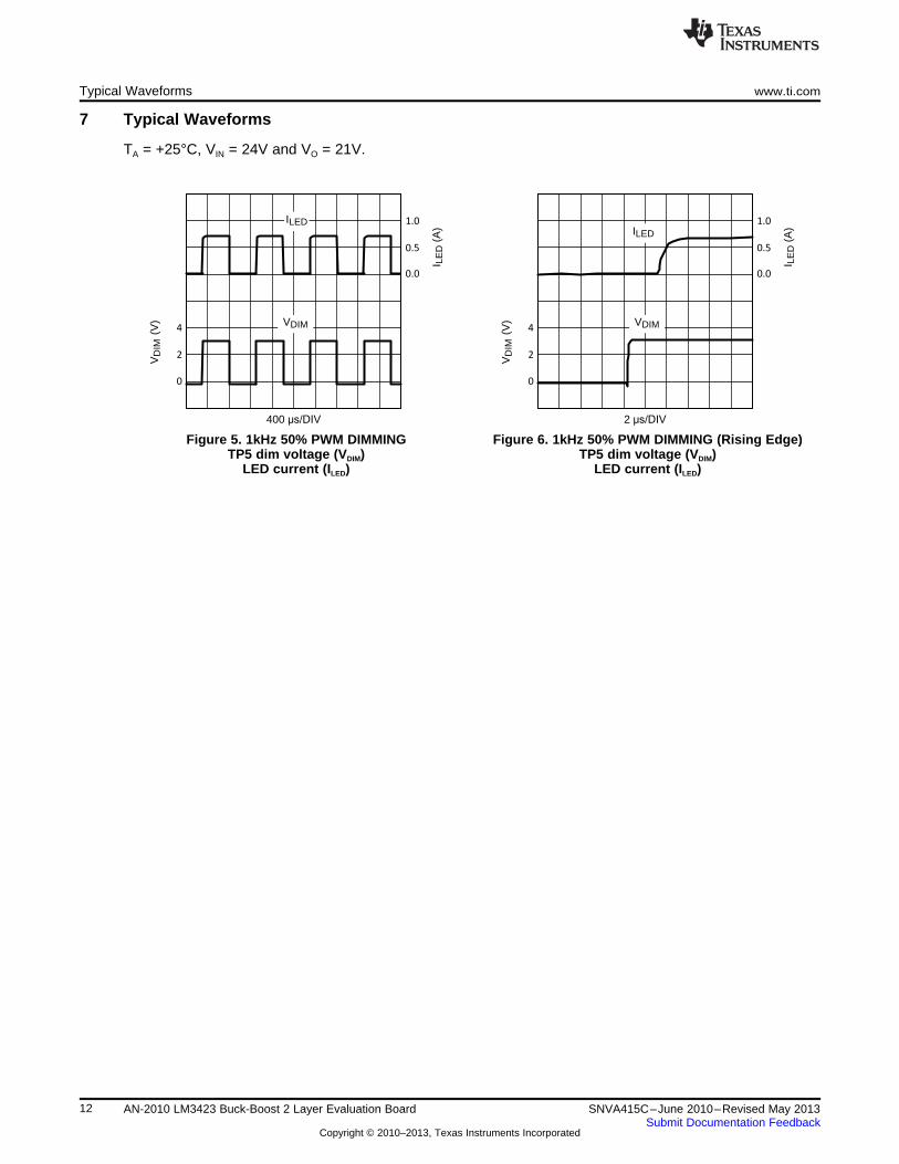
7 Typical Waveforms
TA = +25°C, VIN = 24V and VO = 21V.
Figure 5. 1kHz 50% PWM DIMMING Figure 6. 1kHz 50% PWM DIMMING (Rising Edge)TP5 dim voltage (VDIM) TP5 dim voltage (VDIM)
LED current (ILED) LED current (ILED)
12 AN-2010 LM3423 Buck-Boost 2 Layer Evaluation Board SNVA415C–June 2010–Revised May 2013Submit Documentation Feedback
Copyright © 2010–2013, Texas Instruments Incorporated
C4, C6
Q1
R18
R11
R9
R20
C12
C11
Q5
VIN
Q7
Q6Q4
D2
DIM
R17
R19
DIM Q2
VIN
L1
C9
R6
C8
R1
R10
R13
R5
R8
R7
R4
C7
C2, C3
OVP
nDIM
LM3423
AGND
PGND
DDRV
DAP
GATE
EN
COMP
VIN
CSH
RCT
IS
HSP
RPD
VCC
HSN1
2
3
4
5
6
7
8
20
19
18
17
16
15
14
13
FLT DPOL9 12
TIMR LRDY10 11
R2
C10
R14
VIN
R15
VIN
VCC
VCC
LED-
8
9
10
12
13
14
7
6
5
3
2
1
J7
11 4
D1
LED+
TP1
Q3 PWM
R12
BNC
TP5
TP7RPD
RPDTP4
TP10
GND
J3
R16
C5
C1
R3
J1
J2
J4
J5
J6
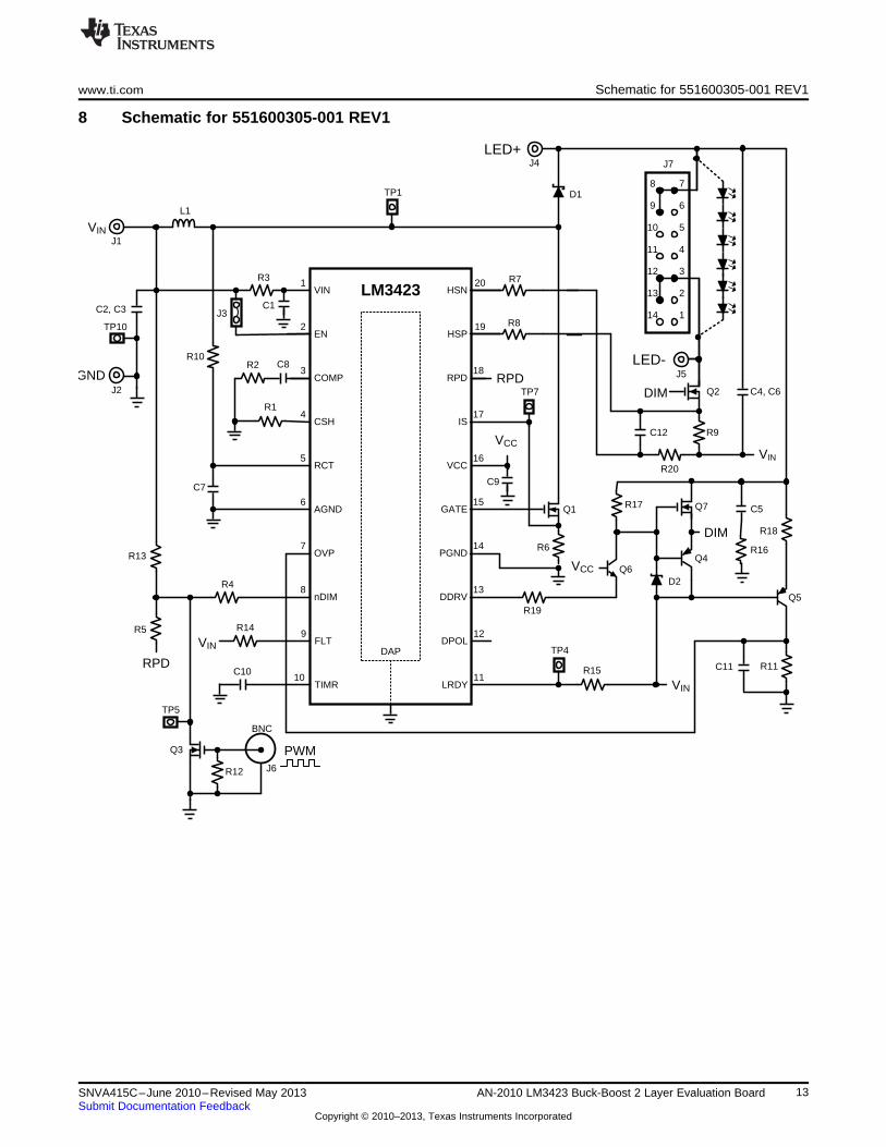
www.ti.com Schematic for 551600305-001 REV1
8 Schematic for 551600305-001 REV1
13SNVA415C–June 2010–Revised May 2013 AN-2010 LM3423 Buck-Boost 2 Layer Evaluation BoardSubmit Documentation Feedback
Copyright © 2010–2013, Texas Instruments Incorporated
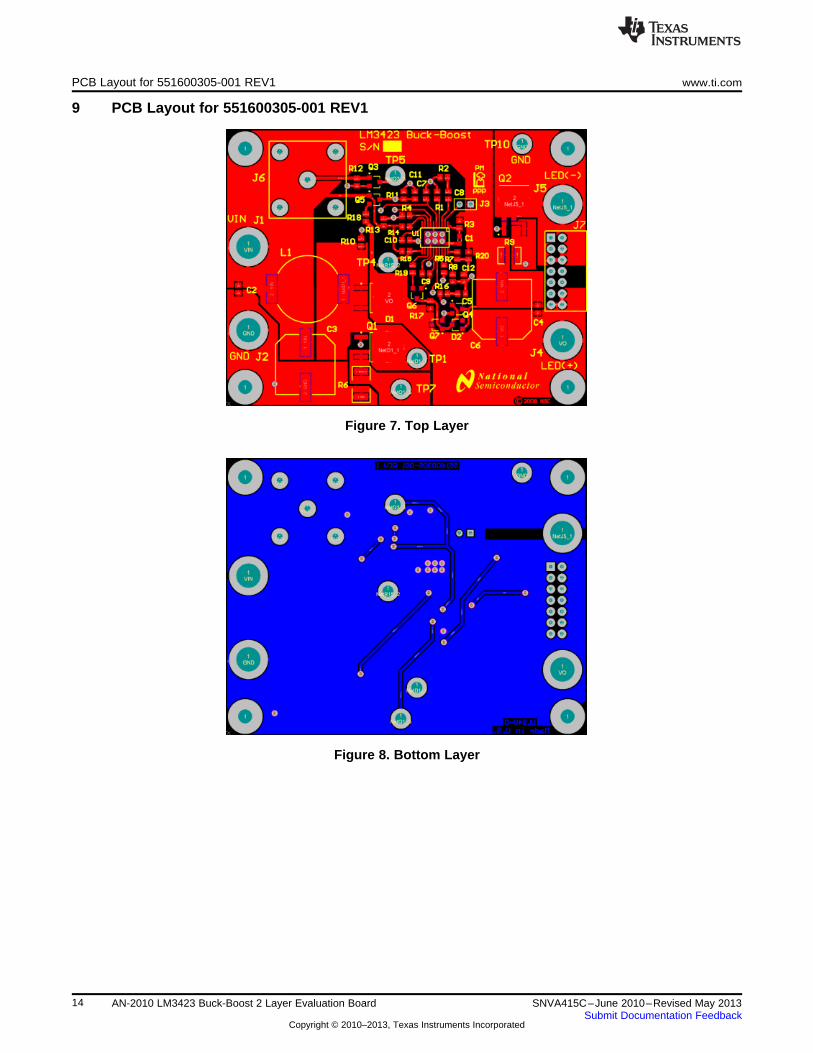
PCB Layout for 551600305-001 REV1 www.ti.com
9 PCB Layout for 551600305-001 REV1
Figure 7. Top Layer
Figure 8. Bottom Layer
14 AN-2010 LM3423 Buck-Boost 2 Layer Evaluation Board SNVA415C–June 2010–Revised May 2013Submit Documentation Feedback
Copyright © 2010–2013, Texas Instruments Incorporated
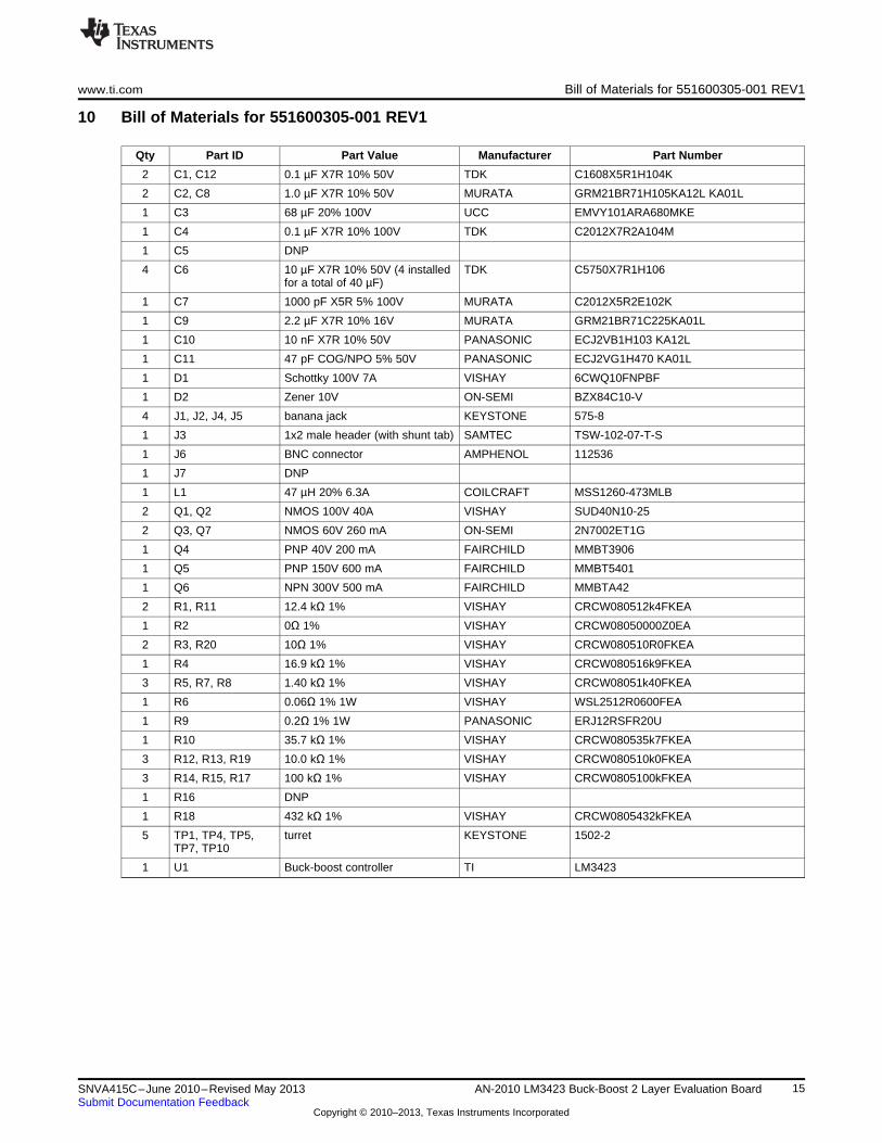
www.ti.com Bill of Materials for 551600305-001 REV1
10 Bill of Materials for 551600305-001 REV1
Qty Part ID Part Value Manufacturer Part Number
2 C1, C12 0.1 µF X7R 10% 50V TDK C1608X5R1H104K
2 C2, C8 1.0 µF X7R 10% 50V MURATA GRM21BR71H105KA12L KA01L
1 C3 68 µF 20% 100V UCC EMVY101ARA680MKE
1 C4 0.1 µF X7R 10% 100V TDK C2012X7R2A104M
1 C5 DNP
4 C6 10 µF X7R 10% 50V (4 installed TDK C5750X7R1H106for a total of 40 µF)
1 C7 1000 pF X5R 5% 100V MURATA C2012X5R2E102K
1 C9 2.2 µF X7R 10% 16V MURATA GRM21BR71C225KA01L
1 C10 10 nF X7R 10% 50V PANASONIC ECJ2VB1H103 KA12L
1 C11 47 pF COG/NPO 5% 50V PANASONIC ECJ2VG1H470 KA01L
1 D1 Schottky 100V 7A VISHAY 6CWQ10FNPBF
1 D2 Zener 10V ON-SEMI BZX84C10-V
4 J1, J2, J4, J5 banana jack KEYSTONE 575-8
1 J3 1x2 male header (with shunt tab) SAMTEC TSW-102-07-T-S
1 J6 BNC connector AMPHENOL 112536
1 J7 DNP
1 L1 47 µH 20% 6.3A COILCRAFT MSS1260-473MLB
2 Q1, Q2 NMOS 100V 40A VISHAY SUD40N10-25
2 Q3, Q7 NMOS 60V 260 mA ON-SEMI 2N7002ET1G
1 Q4 PNP 40V 200 mA FAIRCHILD MMBT3906
1 Q5 PNP 150V 600 mA FAIRCHILD MMBT5401
1 Q6 NPN 300V 500 mA FAIRCHILD MMBTA42
2 R1, R11 12.4 kΩ 1% VISHAY CRCW080512k4FKEA
1 R2 0Ω 1% VISHAY CRCW08050000Z0EA
2 R3, R20 10Ω 1% VISHAY CRCW080510R0FKEA
1 R4 16.9 kΩ 1% VISHAY CRCW080516k9FKEA
3 R5, R7, R8 1.40 kΩ 1% VISHAY CRCW08051k40FKEA
1 R6 0.06Ω 1% 1W VISHAY WSL2512R0600FEA
1 R9 0.2Ω 1% 1W PANASONIC ERJ12RSFR20U
1 R10 35.7 kΩ 1% VISHAY CRCW080535k7FKEA
3 R12, R13, R19 10.0 kΩ 1% VISHAY CRCW080510k0FKEA
3 R14, R15, R17 100 kΩ 1% VISHAY CRCW0805100kFKEA
1 R16 DNP
1 R18 432 kΩ 1% VISHAY CRCW0805432kFKEA
5 TP1, TP4, TP5, turret KEYSTONE 1502-2TP7, TP10
1 U1 Buck-boost controller TI LM3423
15SNVA415C–June 2010–Revised May 2013 AN-2010 LM3423 Buck-Boost 2 Layer Evaluation BoardSubmit Documentation Feedback
Copyright © 2010–2013, Texas Instruments Incorporated
Alternate Designs www.ti.com
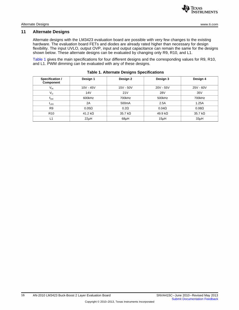
11 Alternate Designs
Alternate designs with the LM3423 evaluation board are possible with very few changes to the existinghardware. The evaluation board FETs and diodes are already rated higher than necessary for designflexibility. The input UVLO, output OVP, input and output capacitance can remain the same for the designsshown below. These alternate designs can be evaluated by changing only R9, R10, and L1.
Table 1 gives the main specifications for four different designs and the corresponding values for R9, R10,and L1. PWM dimming can be evaluated with any of these designs.
Table 1. Alternate Designs Specifications
Specification / Design 1 Design 2 Design 3 Design 4Component
VIN 10V - 45V 15V - 50V 20V - 55V 25V - 60V
VO 14V 21V 28V 35V
fSW 600kHz 700kHz 500kHz 700kHz
ILED 2A 500mA 2.5A 1.25A
R9 0.05Ω 0.2Ω 0.04Ω 0.08ΩR10 41.2 kΩ 35.7 kΩ 49.9 kΩ 35.7 kΩL1 22µH 68µH 15µH 33µH
16 AN-2010 LM3423 Buck-Boost 2 Layer Evaluation Board SNVA415C–June 2010–Revised May 2013Submit Documentation Feedback
Copyright © 2010–2013, Texas Instruments Incorporated

IMPORTANT NOTICE
Texas Instruments Incorporated and its subsidiaries (TI) reserve the right to make corrections, enhancements, improvements and otherchanges to its semiconductor products and services per JESD46, latest issue, and to discontinue any product or service per JESD48, latestissue. Buyers should obtain the latest relevant information before placing orders and should verify that such information is current andcomplete. All semiconductor products (also referred to herein as “components”) are sold subject to TI’s terms and conditions of salesupplied at the time of order acknowledgment.
TI warrants performance of its components to the specifications applicable at the time of sale, in accordance with the warranty in TI’s termsand conditions of sale of semiconductor products. Testing and other quality control techniques are used to the extent TI deems necessaryto support this warranty. Except where mandated by applicable law, testing of all parameters of each component is not necessarilyperformed.
TI assumes no liability for applications assistance or the design of Buyers’ products. Buyers are responsible for their products andapplications using TI components. To minimize the risks associated with Buyers’ products and applications, Buyers should provideadequate design and operating safeguards.
TI does not warrant or represent that any license, either express or implied, is granted under any patent right, copyright, mask work right, orother intellectual property right relating to any combination, machine, or process in which TI components or services are used. Informationpublished by TI regarding third-party products or services does not constitute a license to use such products or services or a warranty orendorsement thereof. Use of such information may require a license from a third party under the patents or other intellectual property of thethird party, or a license from TI under the patents or other intellectual property of TI.
Reproduction of significant portions of TI information in TI data books or data sheets is permissible only if reproduction is without alterationand is accompanied by all associated warranties, conditions, limitations, and notices. TI is not responsible or liable for such altereddocumentation. Information of third parties may be subject to additional restrictions.
Resale of TI components or services with statements different from or beyond the parameters stated by TI for that component or servicevoids all express and any implied warranties for the associated TI component or service and is an unfair and deceptive business practice.TI is not responsible or liable for any such statements.
Buyer acknowledges and agrees that it is solely responsible for compliance with all legal, regulatory and safety-related requirementsconcerning its products, and any use of TI components in its applications, notwithstanding any applications-related information or supportthat may be provided by TI. Buyer represents and agrees that it has all the necessary expertise to create and implement safeguards whichanticipate dangerous consequences of failures, monitor failures and their consequences, lessen the likelihood of failures that might causeharm and take appropriate remedial actions. Buyer will fully indemnify TI and its representatives against any damages arising out of the useof any TI components in safety-critical applications.
In some cases, TI components may be promoted specifically to facilitate safety-related applications. With such components, TI’s goal is tohelp enable customers to design and create their own end-product solutions that meet applicable functional safety standards andrequirements. Nonetheless, such components are subject to these terms.
No TI components are authorized for use in FDA Class III (or similar life-critical medical equipment) unless authorized officers of the partieshave executed a special agreement specifically governing such use.
Only those TI components which TI has specifically designated as military grade or “enhanced plastic” are designed and intended for use inmilitary/aerospace applications or environments. Buyer acknowledges and agrees that any military or aerospace use of TI componentswhich have not been so designated is solely at the Buyer's risk, and that Buyer is solely responsible for compliance with all legal andregulatory requirements in connection with such use.
TI has specifically designated certain components as meeting ISO/TS16949 requirements, mainly for automotive use. In any case of use ofnon-designated products, TI will not be responsible for any failure to meet ISO/TS16949.
Products Applications
Audio www.ti.com/audio Automotive and Transportation www.ti.com/automotive
Amplifiers amplifier.ti.com Communications and Telecom www.ti.com/communications
Data Converters dataconverter.ti.com Computers and Peripherals www.ti.com/computers
DLP® Products www.dlp.com Consumer Electronics www.ti.com/consumer-apps
DSP dsp.ti.com Energy and Lighting www.ti.com/energy
Clocks and Timers www.ti.com/clocks Industrial www.ti.com/industrial
Interface interface.ti.com Medical www.ti.com/medical
Logic logic.ti.com Security www.ti.com/security
Power Mgmt power.ti.com Space, Avionics and Defense www.ti.com/space-avionics-defense
Microcontrollers microcontroller.ti.com Video and Imaging www.ti.com/video
RFID www.ti-rfid.com
OMAP Applications Processors www.ti.com/omap TI E2E Community e2e.ti.com
Wireless Connectivity www.ti.com/wirelessconnectivity
Mailing Address: Texas Instruments, Post Office Box 655303, Dallas, Texas 75265Copyright © 2013, Texas Instruments Incorporated

![A3 P2 A3 P2 A2 5’ A2 5’ A1 P3 A1 P3 2-5A · WTP + 2-5A 0.75 ± 0.06 Y310A + 2-5A 0.54 ± 0.05 crystal + 2-5A 0.36 ± 0.03 [RNase L] μM m, arbitrar y unit s K d Supplementary](https://static.fdocument.org/doc/165x107/606535deb174dc5355677451/a3-p2-a3-p2-a2-5a-a2-5a-a1-p3-a1-p3-2-5a-wtp-2-5a-075-006-y310a-2-5a.jpg)

![arXiv:1207.2303v1 [math.AP] 10 Jul 2012 · dell’Ateneo Lucano 10, I-85100 Potenza, Italy, e-mail: antonio.azzollini@unibas.it z Dipartimento di Matematica, Politecnico di Bari,](https://static.fdocument.org/doc/165x107/60911ee5dabc19250f7c12ac/arxiv12072303v1-mathap-10-jul-2012-dellaateneo-lucano-10-i-85100-potenza.jpg)