Features - Digi-Key Sheets/RFMD PDFs/RF3802.pdfc50 10 μf + c40 10 μf + p1 1 banana jack p1-1 vref...
14
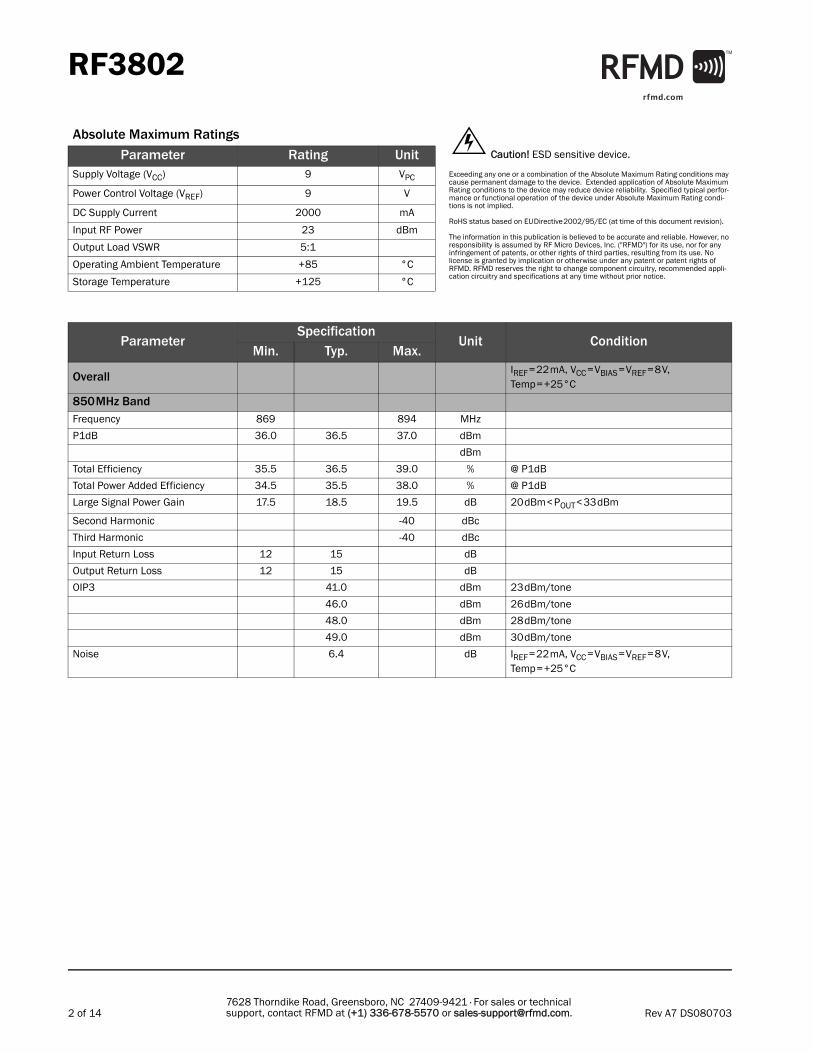
1 of 14 Optimum Technology Matching® Applied GaAs HBT InGaP HBT GaAs MESFET SiGe BiCMOS Si BiCMOS SiGe HBT GaAs pHEMT Si CMOS Si BJT GaN HEMT Functional Block Diagram RF MICRO DEVICES®, RFMD®, Optimum Technology Matching®, Enabling Wireless Connectivity™, PowerStar®, POLARIS™ TOTAL RADIO™ and UltimateBlue™ are trademarks of RFMD, LLC. BLUETOOTH is a trade- mark owned by Bluetooth SIG, Inc., U.S.A. and licensed for use by RFMD. All other trade names, trademarks and registered trademarks are the property of their respective owners. ©2006, RF Micro Devices, Inc. Product Description 7628 Thorndike Road, Greensboro, NC 27409-9421 · For sales or technical support, contact RFMD at (+1) 336-678-5570 or [email protected]. Ordering Information VBIAS VREF VCC1 RF IN RF OUT/VCC2 RF OUT/VCC2 RF OUT/VCC2 RF OUT/VCC2 1 2 3 4 8 7 6 5 PACKAGE BASE GND Bias Circuit RF3802 GaAs HBT PRE-DRIVER AMPLIFIER The RF3802 is specifically designed for wireless infrastructure applications. Using a highly reliable GaAs HBT fabrication process, this high-performance dual-stage amplifier achieves high output power over a broad frequency range. The RF3802 amplifier also provides excellent efficiency and thermal stability through the use of a thermally-enhanced surface-mount AlN package. Ease of integration is accom- plished through the incorporation of an optimized evaluation board design provided to achieve proper 50 Ω operation. Various evaluation board configurations are avail- able to address a broad range of wireless infrastructure applications: • AMPS/GSM850/EDGE850 • GSM900/EDGE900 • IS-95/CDMA2000/AMPS Features 5W Output Power High Linearity 35% Power-Added Efficiency Thermally Enhanced Al N Packag- ing Broadband Platform Design Approach Applications GaAs HBT Pre-Driver for Basesta- tion Amplifiers Power Amplifier Stage for Com- mercial Wireless Infrastructure Class AB Operation for GSM/EDGE/CDMA Transmitter Applications RF3802 GaAs HBT Pre-Driver Amplifier RF3802PCBA-410 Fully Assembled Evaluation Board - GSM850 RF3802PCBA-411 Fully Assembled Evaluation Board - GSM900 Rev A7 DS080703 RF3802GaAs HBT Pre-Driver Amplifier RoHS Compliant & Pb-Free Product Package Style: AlN
-
Upload
dangnguyet -
Category
Documents
-
view
219 -
download
3
Transcript of Features - Digi-Key Sheets/RFMD PDFs/RF3802.pdfc50 10 μf + c40 10 μf + p1 1 banana jack p1-1 vref...
1 of 14
Optimum Technology Matching® Applied
GaAs HBT
InGaP HBTGaAs MESFET
SiGe BiCMOSSi BiCMOSSiGe HBT
GaAs pHEMTSi CMOSSi BJT
GaN HEMT
Functional Block Diagram
RF MICRO DEVICES®, RFMD®, Optimum Technology Matching®, Enabling Wireless Connectivity™, PowerStar®, POLARIS™ TOTAL RADIO™ and UltimateBlue™ are trademarks of RFMD, LLC. BLUETOOTH is a trade-mark owned by Bluetooth SIG, Inc., U.S.A. and licensed for use by RFMD. All other trade names, trademarks and registered trademarks are the property of their respective owners. ©2006, RF Micro Devices, Inc.
Product Description
7628 Thorndike Road, Greensboro, NC 27409-9421 · For sales or technical support, contact RFMD at (+1) 336-678-5570 or [email protected].
Ordering Information
VBIAS
VREF
VCC1
RF IN RF OUT/VCC2
RF OUT/VCC2
RF OUT/VCC2
RF OUT/VCC21
2
3
4
8
7
6
5
PACKAGE BASE
GND
BiasCircuit
RF3802GaAs HBT PRE-DRIVER AMPLIFIER
The RF3802 is specifically designed for wireless infrastructure applications. Usinga highly reliable GaAs HBT fabrication process, this high-performance dual-stageamplifier achieves high output power over a broad frequency range. The RF3802amplifier also provides excellent efficiency and thermal stability through the use ofa thermally-enhanced surface-mount AlN package. Ease of integration is accom-plished through the incorporation of an optimized evaluation board design providedto achieve proper 50Ω operation. Various evaluation board configurations are avail-able to address a broad range of wireless infrastructure applications:
• AMPS/GSM850/EDGE850• GSM900/EDGE900• IS-95/CDMA2000/AMPS
Features5W Output Power
High Linearity
35% Power-Added Efficiency
Thermally Enhanced AlN Packag-ing
Broadband Platform Design Approach
ApplicationsGaAs HBT Pre-Driver for Basesta-tion Amplifiers
Power Amplifier Stage for Com-mercial Wireless Infrastructure
Class AB Operation for GSM/EDGE/CDMA Transmitter Applications
RF3802 GaAs HBT Pre-Driver AmplifierRF3802PCBA-410 Fully Assembled Evaluation Board - GSM850RF3802PCBA-411 Fully Assembled Evaluation Board - GSM900
Rev A7 DS080703
RF3802GaAs HBT Pre-Driver Amplifier
RoHS Compliant & Pb-Free ProductPackage Style: AlN
2 of 14
RF3802
Rev A7 DS0807037628 Thorndike Road, Greensboro, NC 27409-9421 · For sales or technical support, contact RFMD at (+1) 336-678-5570 or [email protected].
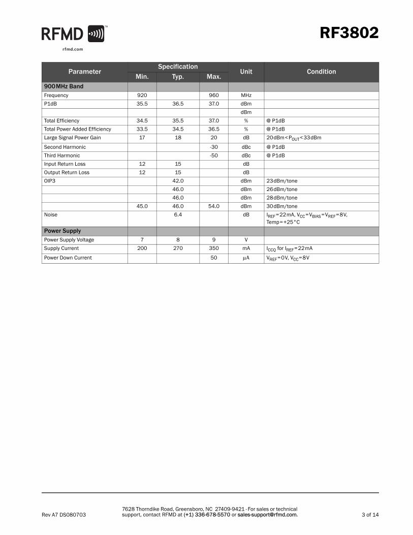
Absolute Maximum Ratings
Parameter Rating UnitSupply Voltage (VCC) 9 VPC
Power Control Voltage (VREF) 9 V
DC Supply Current 2000 mA
Input RF Power 23 dBm
Output Load VSWR 5:1
Operating Ambient Temperature +85 °C
Storage Temperature +125 °C
ParameterSpecification
Unit ConditionMin. Typ. Max.
OverallIREF=22mA, VCC=VBIAS=VREF=8V, Temp=+25°C
850MHz BandFrequency 869 894 MHz
P1dB 36.0 36.5 37.0 dBm
dBm
Total Efficiency 35.5 36.5 39.0 % @ P1dB
Total Power Added Efficiency 34.5 35.5 38.0 % @ P1dB
Large Signal Power Gain 17.5 18.5 19.5 dB 20dBm<POUT<33dBm
Second Harmonic -40 dBc
Third Harmonic -40 dBc
Input Return Loss 12 15 dB
Output Return Loss 12 15 dB
OIP3 41.0 dBm 23dBm/tone
46.0 dBm 26dBm/tone
48.0 dBm 28dBm/tone
49.0 dBm 30dBm/tone
Noise 6.4 dB IREF=22mA, VCC=VBIAS=VREF=8V, Temp=+25°C
Caution! ESD sensitive device.
Exceeding any one or a combination of the Absolute Maximum Rating conditions may cause permanent damage to the device. Extended application of Absolute Maximum Rating conditions to the device may reduce device reliability. Specified typical perfor-mance or functional operation of the device under Absolute Maximum Rating condi-tions is not implied.
RoHS status based on EUDirective2002/95/EC (at time of this document revision).
The information in this publication is believed to be accurate and reliable. However, no responsibility is assumed by RF Micro Devices, Inc. ("RFMD") for its use, nor for any infringement of patents, or other rights of third parties, resulting from its use. No license is granted by implication or otherwise under any patent or patent rights of RFMD. RFMD reserves the right to change component circuitry, recommended appli-cation circuitry and specifications at any time without prior notice.
3 of 14
RF3802
Rev A7 DS0807037628 Thorndike Road, Greensboro, NC 27409-9421 · For sales or technical support, contact RFMD at (+1) 336-678-5570 or [email protected].
ParameterSpecification
Unit ConditionMin. Typ. Max.
900MHz BandFrequency 920 960 MHz
P1dB 35.5 36.5 37.0 dBm
dBm
Total Efficiency 34.5 35.5 37.0 % @ P1dB
Total Power Added Efficiency 33.5 34.5 36.5 % @ P1dB
Large Signal Power Gain 17 18 20 dB 20dBm<POUT<33dBm
Second Harmonic -30 dBc @ P1dB
Third Harmonic -50 dBc @ P1dB
Input Return Loss 12 15 dB
Output Return Loss 12 15 dB
OIP3 42.0 dBm 23dBm/tone
46.0 dBm 26dBm/tone
46.0 dBm 28dBm/tone
45.0 46.0 54.0 dBm 30dBm/tone
Noise 6.4 dB IREF=22mA, VCC=VBIAS=VREF=8V, Temp=+25°C
Power SupplyPower Supply Voltage 7 8 9 V
Supply Current 200 270 350 mA ICCQ for IREF=22mA
Power Down Current 50 μA VREF=0V, VCC=8V
4 of 14
RF3802
Rev A7 DS0807037628 Thorndike Road, Greensboro, NC 27409-9421 · For sales or technical support, contact RFMD at (+1) 336-678-5570 or [email protected].
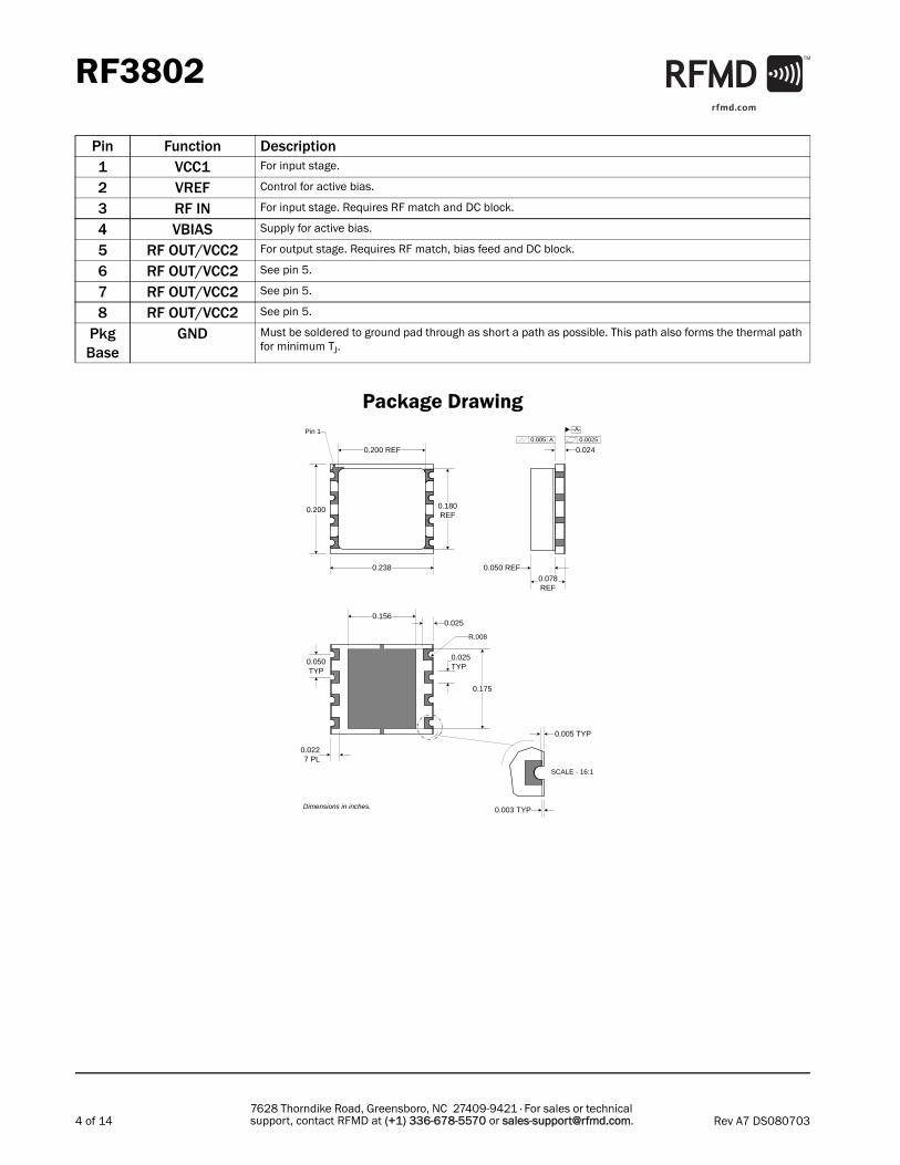
Package Drawing
Pin Function Description1 VCC1 For input stage.
2 VREF Control for active bias.
3 RF IN For input stage. Requires RF match and DC block.
4 VBIAS Supply for active bias.
5 RF OUT/VCC2 For output stage. Requires RF match, bias feed and DC block.
6 RF OUT/VCC2 See pin 5.
7 RF OUT/VCC2 See pin 5.
8 RF OUT/VCC2 See pin 5.
Pkg Base
GND Must be soldered to ground pad through as short a path as possible. This path also forms the thermal path for minimum TJ.
Dimensions in inches.
0.050TYP
0.0227 PL
0.025TYP
0.175
R.008
0.0250.156
SCALE - 16:1
0.003 TYP
0.005 TYP
Pin 1
0.238
0.200 REF
0.200 0.180REF
0.0025
0.0240.005 A
-A-
0.078REF
0.050 REF
5 of 14
RF3802
Rev A7 DS0807037628 Thorndike Road, Greensboro, NC 27409-9421 · For sales or technical support, contact RFMD at (+1) 336-678-5570 or [email protected].
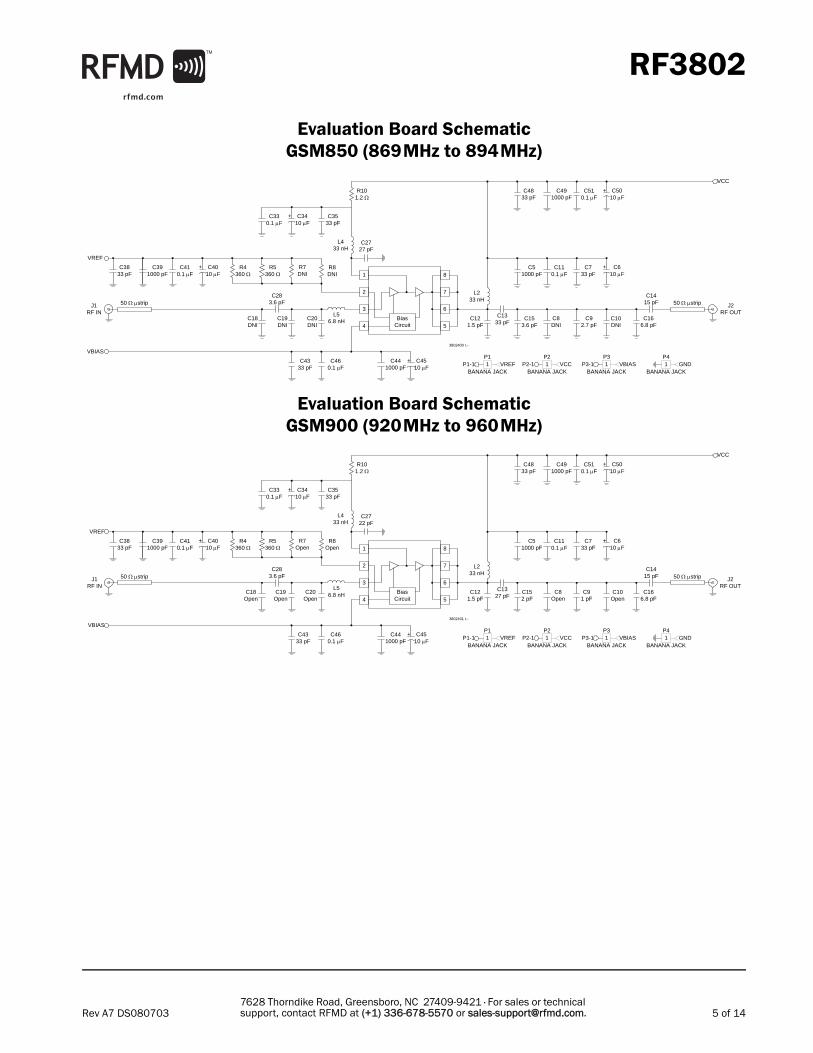
Evaluation Board SchematicGSM850 (869MHz to 894MHz)
Evaluation Board SchematicGSM900 (920MHz to 960MHz)
VCC
L56.8 nH
C460.1 μF
C4333 pF
C121.5 pF
C153.6 pF
L433 nH
R7DNI
R8DNI
VBIAS3802400 r.-
BiasCircuit
1
2
3
4
8
7
6
5
C3533 pF
C330.1 μF
R4360 Ω
R5360 Ω
C391000 pF
C3833 pF
C410.1 μF
VREF
C20DNI
C19DNI
50 Ω μstripJ1RF IN
C283.6 pF
C18DNI
C4510 μF
+C441000 pF
C8DNI
C92.7 pF
C1415 pF
C166.8 pF
L233 nH
C1333 pF
C10DNI
J2RF OUT
50 Ω μstrip
C51000 pF
C733 pF
C110.1 μF
C610 μF
+
C4833 pF
C491000 pF
C510.1 μF
C2727 pF
R101.2 Ω
C3410 μF
+
C5010 μF
+
C4010 μF
+
P11
BANANA JACKP1-1 VREF
P41
BANANA JACKGND
P21
BANANA JACKP2-1 VCC
P31
BANANA JACKP3-1 VBIAS
VCC
L56.8 nH
C460.1 μF
C4333 pF
C121.5 pF
C152 pF
L433 nH
R7Open
R8Open
VBIAS3802401 r.-
BiasCircuit
1
2
3
4
8
7
6
5
C3533 pF
C330.1 μF
R4360 Ω
R5360 Ω
C391000 pF
C3833 pF
C410.1 μF
VREF
C20Open
C19Open
50 Ω μstripJ1RF IN
C283.6 pF
C18Open
C4510 μF
+C441000 pF
C8Open
C91 pF
C1415 pF
C166.8 pF
L233 nH
C1327 pF
C10Open
J2RF OUT
50 Ω μstrip
C51000 pF
C733 pF
C110.1 μF
C610 μF
+
C4833 pF
C491000 pF
C510.1 μF
C2722 pF
R101.2 Ω
C3410 μF
+
C5010 μF
+
C4010 μF
+
P11
BANANA JACKP1-1 VREF
P41
BANANA JACKGND
P21
BANANA JACKP2-1 VCC
P31
BANANA JACKP3-1 VBIAS
6 of 14
RF3802
Rev A7 DS0807037628 Thorndike Road, Greensboro, NC 27409-9421 · For sales or technical support, contact RFMD at (+1) 336-678-5570 or [email protected].
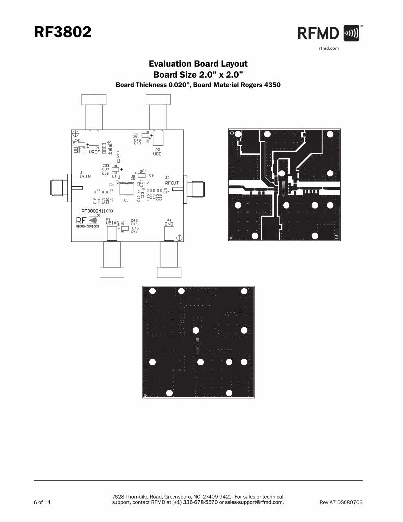
Evaluation Board LayoutBoard Size 2.0” x 2.0”
Board Thickness 0.020”, Board Material Rogers 4350
7 of 14
RF3802
Rev A7 DS0807037628 Thorndike Road, Greensboro, NC 27409-9421 · For sales or technical support, contact RFMD at (+1) 336-678-5570 or [email protected].
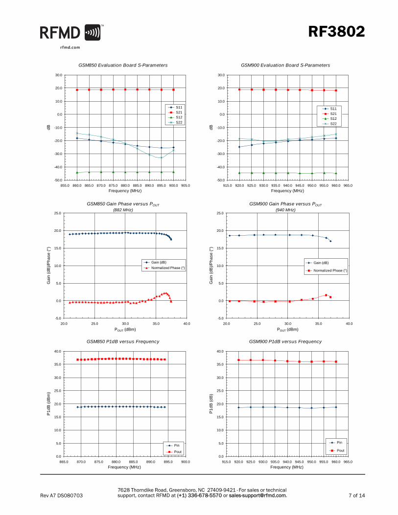
GSM850 Gain Phase versus POUT
(882 MHz)
-5.0
0.0
5.0
10.0
15.0
20.0
25.0
20.0 25.0 30.0 35.0 40.0
POUT (dBm)
Ga
in (d
B)/
Ph
ase
(°)
Gain (dB)
Normalized Phase (°)
GSM850 P1dB versus Frequency
0.0
5.0
10.0
15.0
20.0
25.0
30.0
35.0
40.0
865.0 870.0 875.0 880.0 885.0 890.0 895.0 900.0
Frequency (MHz)
P1d
B (
dBm
)
Pin
Pout
GSM900 Gain Phase versus POUT
(940 MHz)
-5.0
0.0
5.0
10.0
15.0
20.0
25.0
20.0 25.0 30.0 35.0 40.0
POUT (dBm)
Ga
in (d
B)/
Ph
ase
(°)
Gain (dB)
Normalized Phase (°)
GSM900 P1dB versus Frequency
0.0
5.0
10.0
15.0
20.0
25.0
30.0
35.0
40.0
915.0 920.0 925.0 930.0 935.0 940.0 945.0 950.0 955.0 960.0 965.0
Frequency (MHz)
P1
dB (d
B)
Pin
Pout
GSM900 Evaluation Board S-Parameters
-50.0
-40.0
-30.0
-20.0
-10.0
0.0
10.0
20.0
30.0
915.0 920.0 925.0 930.0 935.0 940.0 945.0 950.0 955.0 960.0 965.0
Frequency (MHz)
dB
S11 S21 S12 S22
GSM850 Evaluation Board S-Parameters
-50.0
-40.0
-30.0
-20.0
-10.0
0.0
10.0
20.0
30.0
855.0 860.0 865.0 870.0 875.0 880.0 885.0 890.0 895.0 900.0 905.0
Frequency (MHz)
dB
S11 S21 S12 S22
8 of 14
RF3802
Rev A7 DS0807037628 Thorndike Road, Greensboro, NC 27409-9421 · For sales or technical support, contact RFMD at (+1) 336-678-5570 or [email protected].
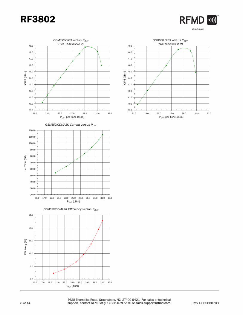
GSM850 OIP3 versus POUT
(Two-Tone 882 MHz)
39.0
40.0
41.0
42.0
43.0
44.0
45.0
46.0
47.0
48.0
49.0
21.0 23.0 25.0 27.0 29.0 31.0 33.0
POUT per Tone (dBm)
OIP
3 (d
Bm
)
GSM850/CDMA2K Efficiency versus POUT
0.0
5.0
10.0
15.0
20.0
25.0
15.0 17.0 19.0 21.0 23.0 25.0 27.0 29.0 31.0 33.0 35.0
POUT (dBm)
Effi
cien
cy (%
)
GSM900 OIP3 versus POUT
(Two-Tone 940 MHz)
39.0
40.0
41.0
42.0
43.0
44.0
45.0
46.0
47.0
48.0
49.0
21.0 23.0 25.0 27.0 29.0 31.0 33.0
POUT per Tone (dBm)
OIP
3 (d
Bm
)GSM850/CDMA2K Current versus POUT
200.0
300.0
400.0
500.0
600.0
700.0
800.0
900.0
1000.0
1100.0
1200.0
15.0 17.0 19.0 21.0 23.0 25.0 27.0 29.0 31.0 33.0 35.0
POUT (dBm)
I CC T
otal
(mA
)
9 of 14
RF3802
Rev A7 DS0807037628 Thorndike Road, Greensboro, NC 27409-9421 · For sales or technical support, contact RFMD at (+1) 336-678-5570 or [email protected].
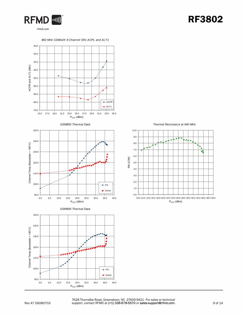
GSM850 Thermal Data
90.0
100.0
110.0
120.0
130.0
140.0
150.0
0.0 5.0 10.0 15.0 20.0 25.0 30.0 35.0 40.0
POUT (dBm)
Cha
nnel
Tem
p (B
asep
late
= +
85°C
)
PA
Driver
GSM900 Thermal Data
90.0
100.0
110.0
120.0
130.0
140.0
150.0
0.0 5.0 10.0 15.0 20.0 25.0 30.0 35.0 40.0
POUT (dBm)
Cha
nnel
Tem
p (B
asep
late
= +
85°C
)
PA
Driver
882 MHz CDMA2K 9-Channel SR1 ACPL and ALT1
-70.0
-65.0
-60.0
-55.0
-50.0
-45.0
-40.0
-35.0
-30.0
15.0 17.0 19.0 21.0 23.0 25.0 27.0 29.0 31.0 33.0 35.0
POUT (dBm)
AC
PR
and
ALT
1 (d
Bc)
ACPR
ALT1
Thermal Resistance at 940 MHz
0.0
1.0
2.0
3.0
4.0
5.0
6.0
7.0
8.0
9.0
10.0
10.0 12.0 14.0 16.0 18.0 20.0 22.0 24.0 26.0 28.0 30.0 32.0 34.0 36.0 38.0 40.0
POUT (dBm)
Rth
(C/W
)
10 of 14
RF3802
Rev A7 DS0807037628 Thorndike Road, Greensboro, NC 27409-9421 · For sales or technical support, contact RFMD at (+1) 336-678-5570 or [email protected].
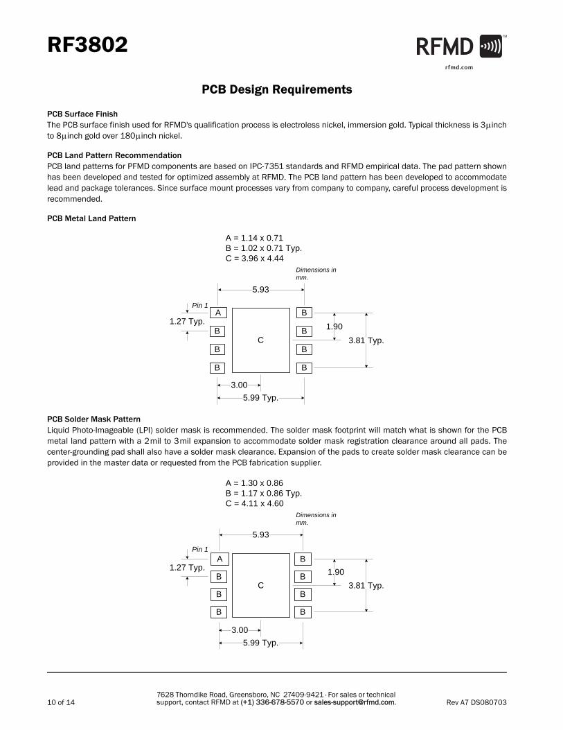
PCB Design Requirements
PCB Surface FinishThe PCB surface finish used for RFMD's qualification process is electroless nickel, immersion gold. Typical thickness is 3μinchto 8μinch gold over 180μinch nickel.
PCB Land Pattern RecommendationPCB land patterns for PFMD components are based on IPC-7351 standards and RFMD empirical data. The pad pattern shownhas been developed and tested for optimized assembly at RFMD. The PCB land pattern has been developed to accommodatelead and package tolerances. Since surface mount processes vary from company to company, careful process development isrecommended.
PCB Metal Land Pattern
PCB Solder Mask PatternLiquid Photo-Imageable (LPI) solder mask is recommended. The solder mask footprint will match what is shown for the PCBmetal land pattern with a 2mil to 3mil expansion to accommodate solder mask registration clearance around all pads. Thecenter-grounding pad shall also have a solder mask clearance. Expansion of the pads to create solder mask clearance can beprovided in the master data or requested from the PCB fabrication supplier.
A = 1.14 x 0.71B = 1.02 x 0.71 Typ.C = 3.96 x 4.44
Dimensions in mm.
C
A
B
B
B
B
B
B
B
Pin 1
5.93
1.27 Typ.
5.99 Typ.
3.00
3.81 Typ.
1.90
A = 1.30 x 0.86B = 1.17 x 0.86 Typ.C = 4.11 x 4.60
Dimensions in mm.
5.93
Pin 1A
CB
B
B
B
B
B
B
1.27 Typ.
5.99 Typ.
3.00
3.81 Typ.
1.90
11 of 14
RF3802
Rev A7 DS0807037628 Thorndike Road, Greensboro, NC 27409-9421 · For sales or technical support, contact RFMD at (+1) 336-678-5570 or [email protected].
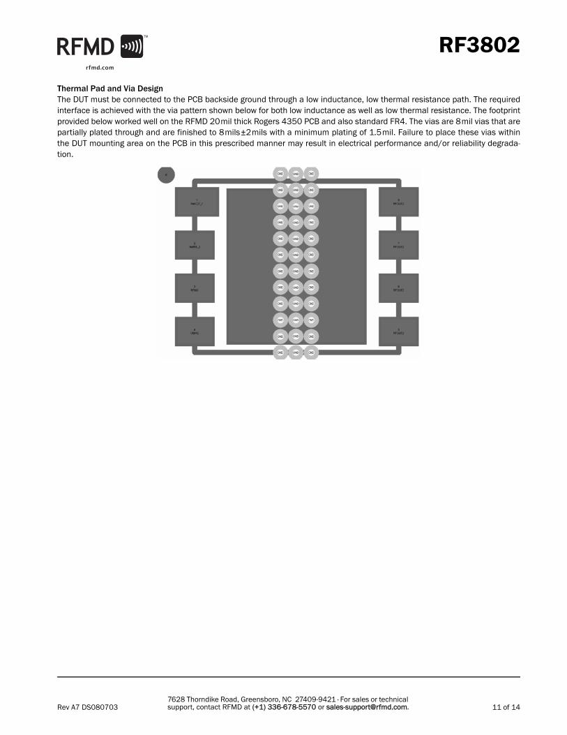
Thermal Pad and Via DesignThe DUT must be connected to the PCB backside ground through a low inductance, low thermal resistance path. The requiredinterface is achieved with the via pattern shown below for both low inductance as well as low thermal resistance. The footprintprovided below worked well on the RFMD 20mil thick Rogers 4350 PCB and also standard FR4. The vias are 8mil vias that arepartially plated through and are finished to 8mils±2mils with a minimum plating of 1.5mil. Failure to place these vias withinthe DUT mounting area on the PCB in this prescribed manner may result in electrical performance and/or reliability degrada-tion.
12 of 14
RF3802
Rev A7 DS0807037628 Thorndike Road, Greensboro, NC 27409-9421 · For sales or technical support, contact RFMD at (+1) 336-678-5570 or [email protected].
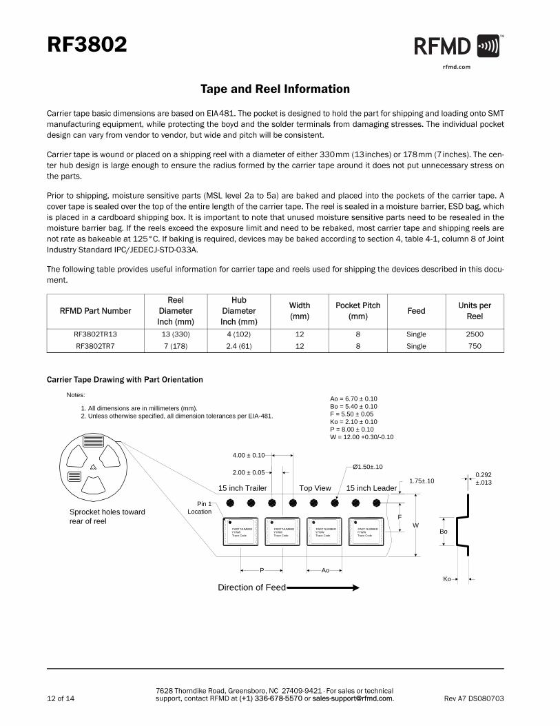
Tape and Reel Information
Carrier tape basic dimensions are based on EIA481. The pocket is designed to hold the part for shipping and loading onto SMTmanufacturing equipment, while protecting the boyd and the solder terminals from damaging stresses. The individual pocketdesign can vary from vendor to vendor, but wide and pitch will be consistent.
Carrier tape is wound or placed on a shipping reel with a diameter of either 330mm (13inches) or 178mm (7inches). The cen-ter hub design is large enough to ensure the radius formed by the carrier tape around it does not put unnecessary stress onthe parts.
Prior to shipping, moisture sensitive parts (MSL level 2a to 5a) are baked and placed into the pockets of the carrier tape. Acover tape is sealed over the top of the entire length of the carrier tape. The reel is sealed in a moisture barrier, ESD bag, whichis placed in a cardboard shipping box. It is important to note that unused moisture sensitive parts need to be resealed in themoisture barrier bag. If the reels exceed the exposure limit and need to be rebaked, most carrier tape and shipping reels arenot rate as bakeable at 125°C. If baking is required, devices may be baked according to section 4, table 4-1, column 8 of JointIndustry Standard IPC/JEDECJ-STD-033A.
The following table provides useful information for carrier tape and reels used for shipping the devices described in this docu-ment.
Carrier Tape Drawing with Part Orientation
RFMD Part NumberReel
Diameter Inch (mm)
Hub Diameter Inch (mm)
Width (mm)
Pocket Pitch(mm)
FeedUnits per
Reel
RF3802TR13 13 (330) 4 (102) 12 8 Single 2500
RF3802TR7 7 (178) 2.4 (61) 12 8 Single 750
4.00 ± 0.10
1.75±.100.292±.013
Sprocket holes towardrear of reel
15 inch Trailer Top View 15 inch Leader
Pin 1Location
Ø1.50±.10
PART NUMBERYYWWTrace Code
PART NUMBERYYWWTrace Code
PART NUMBERYYWWTrace Code
PART NUMBERYYWWTrace Code
WF
Bo
KoAoP
2.00 ± 0.05
Notes:
1. All dimensions are in millimeters (mm).2. Unless otherwise specified, all dimension tolerances per EIA-481.
Direction of Feed
Ao = 6.70 ± 0.10Bo = 5.40 ± 0.10F = 5.50 ± 0.05Ko = 2.10 ± 0.10P = 8.00 ± 0.10W = 12.00 +0.30/-0.10
13 of 14
RF3802
Rev A7 DS0807037628 Thorndike Road, Greensboro, NC 27409-9421 · For sales or technical support, contact RFMD at (+1) 336-678-5570 or [email protected].
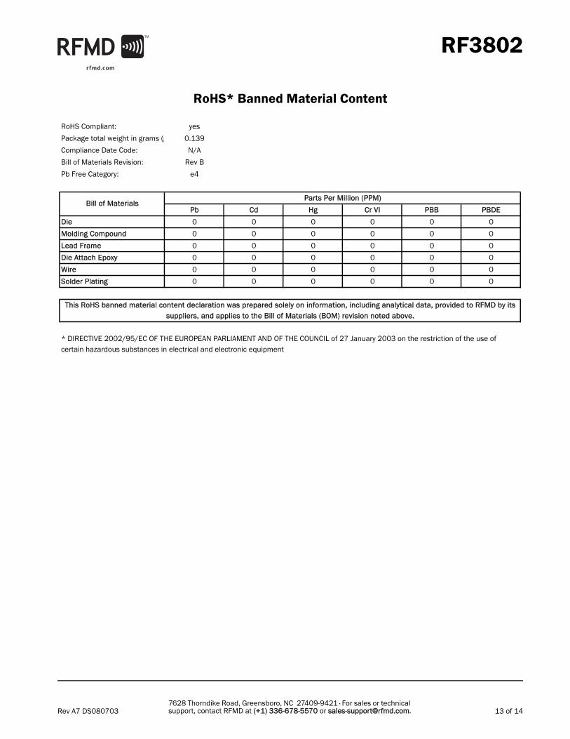
RoHS Compliant: yes
Package total weight in grams (g 0.139
Compliance Date Code: N/A
Bill of Materials Revision: Rev B
Pb Free Category: e4
Pb Cd Hg Cr VI PBB PBDE
Die 0 0 0 0 0 0
Molding Compound 0 0 0 0 0 0
Lead Frame 0 0 0 0 0 0
Die Attach Epoxy 0 0 0 0 0 0
Wire 0 0 0 0 0 0
Solder Plating 0 0 0 0 0 0
* DIRECTIVE 2002/95/EC OF THE EUROPEAN PARLIAMENT AND OF THE COUNCIL of 27 January 2003 on the restriction of the use of certain hazardous substances in electrical and electronic equipment
RoHS* Banned Material Content
Bill of MaterialsParts Per Million (PPM)
This RoHS banned material content declaration was prepared solely on information, including analytical data, provided to RFMD by its suppliers, and applies to the Bill of Materials (BOM) revision noted above.
14 of 14
RF3802
Rev A7 DS0807037628 Thorndike Road, Greensboro, NC 27409-9421 · For sales or technical support, contact RFMD at (+1) 336-678-5570 or [email protected].