Advanced SiC/GaN 3-ΦPWM Inverter Systems for VSD Applications · Bearings / Shaft Grndg Brushes /...
60
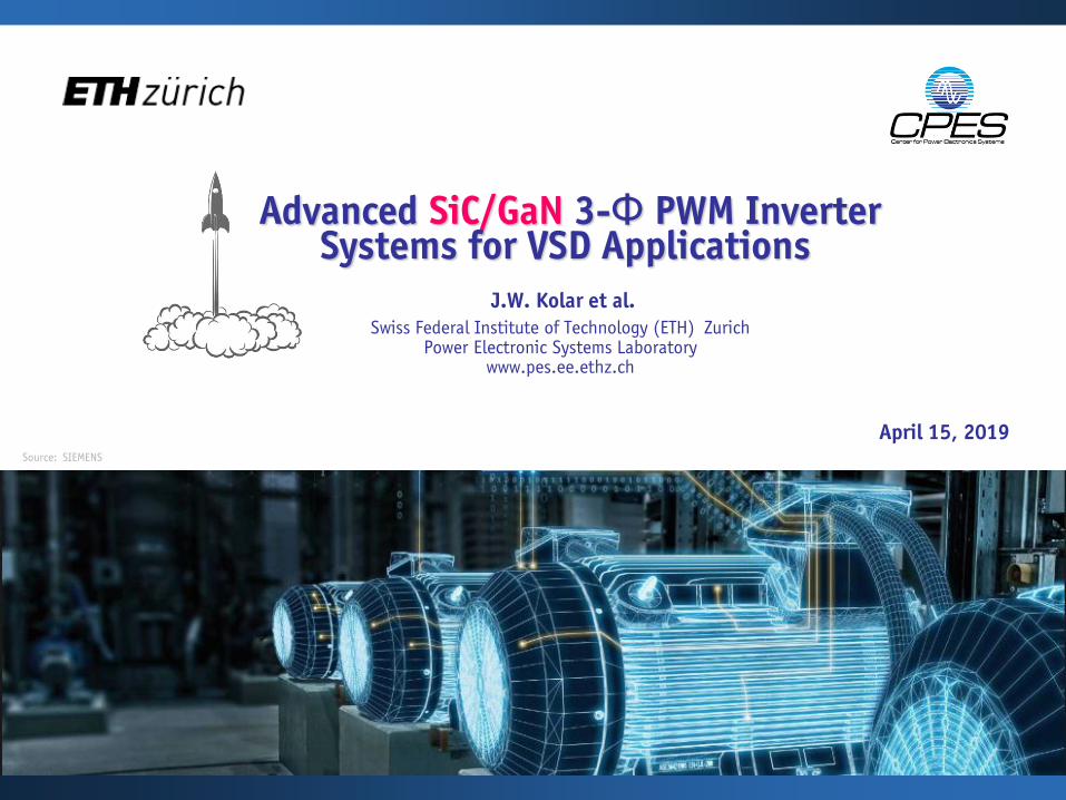
April 15, 2019 Source: SIEMENS J.W. Kolar et al. Swiss Federal Institute of Technology (ETH) Zurich Power Electronic Systems Laboratory www.pes.ee.ethz.ch Advanced SiC / GaN 3 - Φ PWM Inverter Systems for VSD Applications
Transcript of Advanced SiC/GaN 3-ΦPWM Inverter Systems for VSD Applications · Bearings / Shaft Grndg Brushes /...
April 15, 2019Source: SIEMENS
J.W. Kolar et al.Swiss Federal Institute of Technology (ETH) Zurich
Power Electronic Systems Laboratorywww.pes.ee.ethz.ch
Advanced SiC/GaN 3-Φ PWM Inverter Systems for VSD Applications

J.W. Kolar, M. Guacci, M. Antivachis, D. BortisSwiss Federal Institute of Technology (ETH) Zurich
Power Electronic Systems Laboratorywww.pes.ee.ethz.ch
April 15, 2019Source: SIEMENS
Advanced SiC/GaN 3-Φ PWM Inverter Systems for VSD Applications
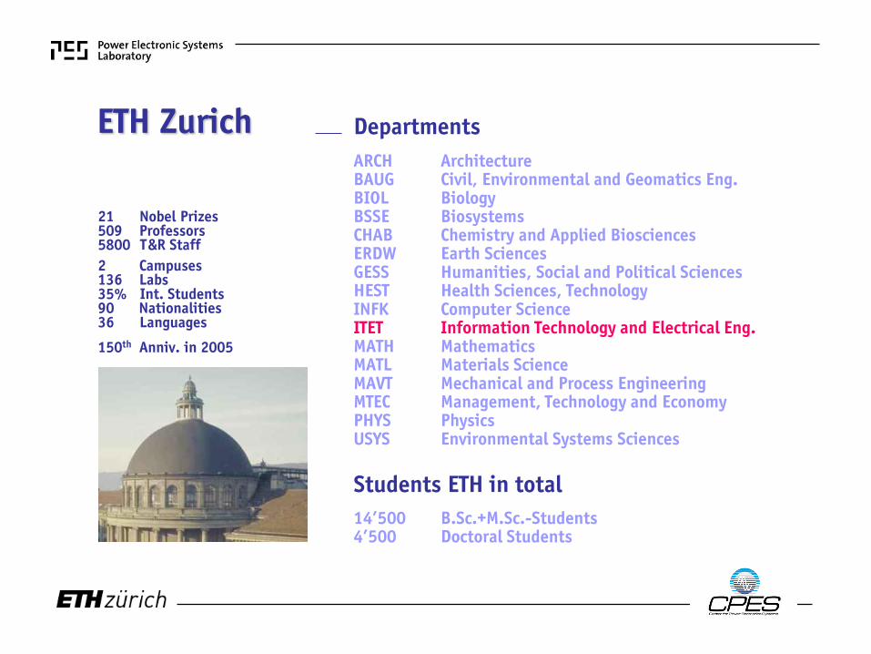
Departments ARCH Architecture BAUG Civil, Environmental and Geomatics Eng.BIOL BiologyBSSE BiosystemsCHAB Chemistry and Applied BiosciencesERDW Earth SciencesGESS Humanities, Social and Political Sciences HEST Health Sciences, TechnologyINFK Computer Science ITET Information Technology and Electrical Eng.MATH MathematicsMATL Materials Science MAVT Mechanical and Process Engineering MTEC Management, Technology and EconomyPHYS Physics USYS Environmental Systems Sciences
Students ETH in total14’500 B.Sc.+M.Sc.-Students4’500 Doctoral Students
21 Nobel Prizes509 Professors5800 T&R Staff2 Campuses136 Labs35% Int. Students90 Nationalities36 Languages
150th Anniv. in 2005
ETH Zurich
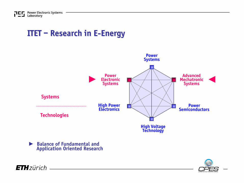
High Power Electronics
► Balance of Fundamental andApplication Oriented Research
Power Semiconductors
Power Systems
AdvancedMechatronic
Systems
High Voltage Technology
Power Electronic Systems►
►
ITET – Research in E-Energy
Systems
Technologies
DC-ACConverter
Johann W. Kolar
AC-DC Converter
M. HellerD. Menzi
D. Neumayr
DC-DC Converter
P. BezerraT. Guillod
G. KnabbenJ. Schäfer
Industry RelationsR. Coccia / B. Seiler
AC-ACConverter
J. AzurzaP. Czyz
M. Haider
Multi-DomainModeling
AdvancedMechatronics
E. Hubmann
SecretariatM. Kohn / Y. Schnyder
AdministrationP. Maurantonio
Computer SystemsM. Eisenstat
Electronics LaboratoryP. Seitz
P. Niklaus
19 Ph.D. Students2 Sen. Researchers
Leading Univ.in Europe
F. Krismer
Magnetic Levitation
MeasurementTechnology
D. Bortis
Th. HolensteinP. Püntener
S. Miric
M. AntivachisJ. BöhlerM. Guacci
P. Papamanolis
Adv. Mechatronic SystemsD. Bortis
D. BortisD. Bortis F. Krismer
Power Electronic Systems Laboratory
Outline► Introduction ► SiC/GaN Application Challenge► Inverters with Output Filter► Adv. Inverter Topologies► Conclusions
1/44
J. AzurzaT. GuillodF. Krismer
D. MenziJ. Miniböck
Acknowledgement: P. Niklaus
State-of-the-ArtFuture Requirements
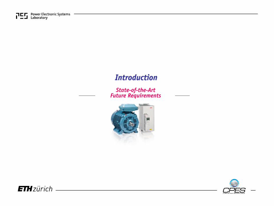
Introduction
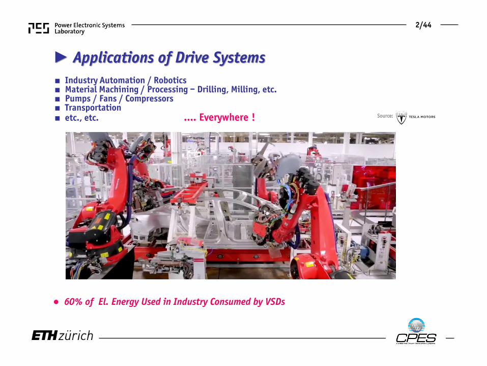
► Applications of Drive Systems ■ Industry Automation / Robotics■ Material Machining / Processing – Drilling, Milling, etc. ■ Pumps / Fans / Compressors■ Transportation■ etc., etc. …. Everywhere ! Source:
● 60% of El. Energy Used in Industry Consumed by VSDs
2/44
► State-of-the-Art
● High Performance @ High Level of Complexity / High Costs (!)
3/44
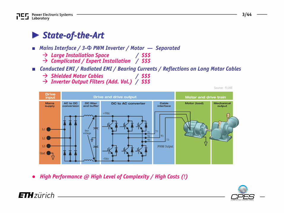
■ Mains Interface / 3-Φ PWM Inverter / Motor — Separated Large Installation Space / $$$ Complicated / Expert Installation / $$$
Source: ABB
Source: FLUKE
■ Conducted EMI / Radiated EMI / Bearing Currents / Reflections on Long Motor Cables Shielded Motor Cables / $$$ Inverter Output Filters (Add. Vol.) / $$$
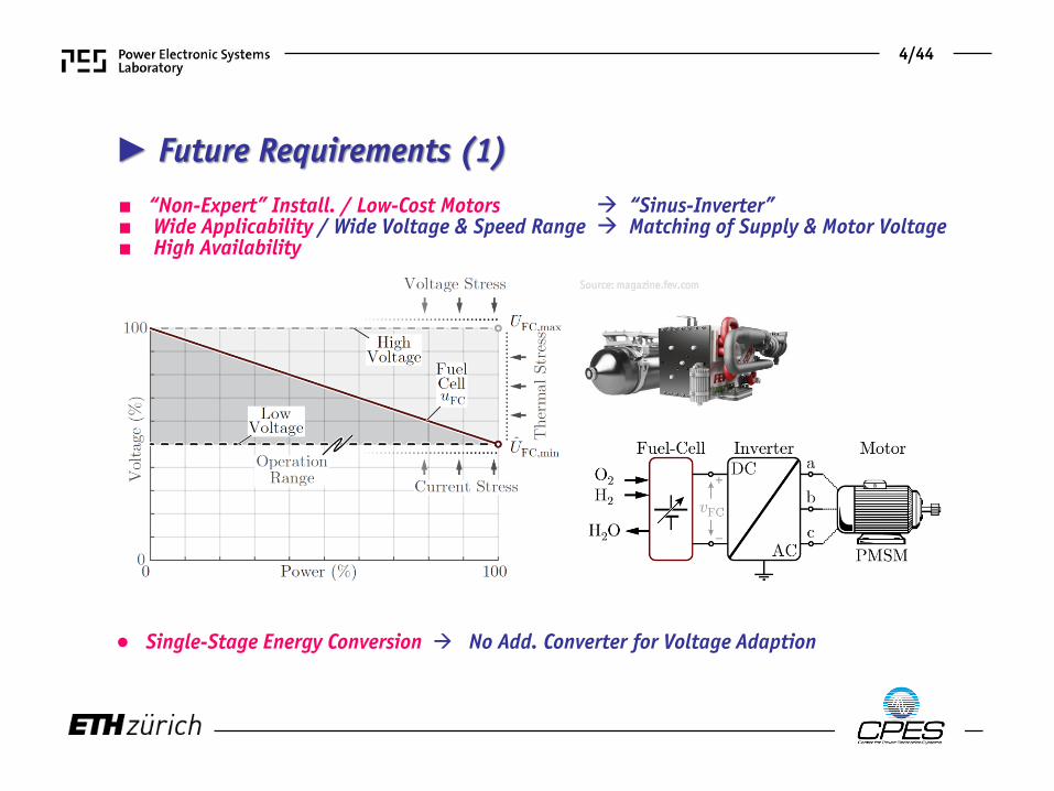
■ “Non-Expert” Install. / Low-Cost Motors “Sinus-Inverter”■ Wide Applicability / Wide Voltage & Speed Range Matching of Supply & Motor Voltage■ High Availability
● Single-Stage Energy Conversion No Add. Converter for Voltage Adaption
4/44
Source: magazine.fev.com
► Future Requirements (1)
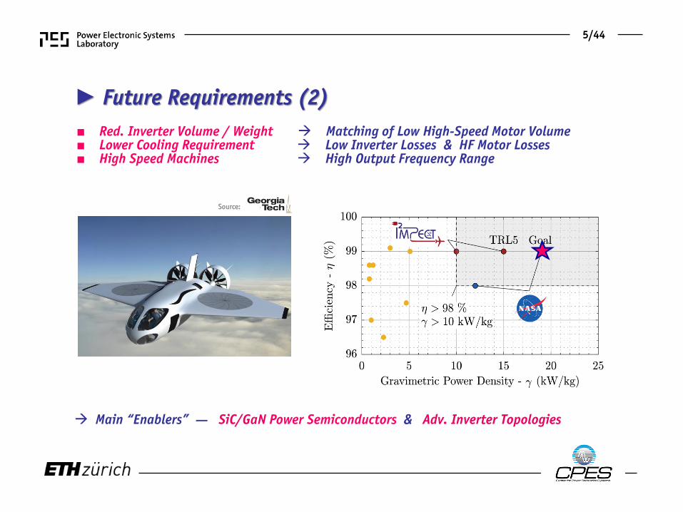
► Future Requirements (2) ■ Red. Inverter Volume / Weight Matching of Low High-Speed Motor Volume ■ Lower Cooling Requirement Low Inverter Losses & HF Motor Losses■ High Speed Machines High Output Frequency Range
Main “Enablers” — SiC/GaN Power Semiconductors & Adv. Inverter Topologies
5/44
Source:
WBG SemiconductorsAdvanced Inverter Topologies
Enabling Technologies & Challenges
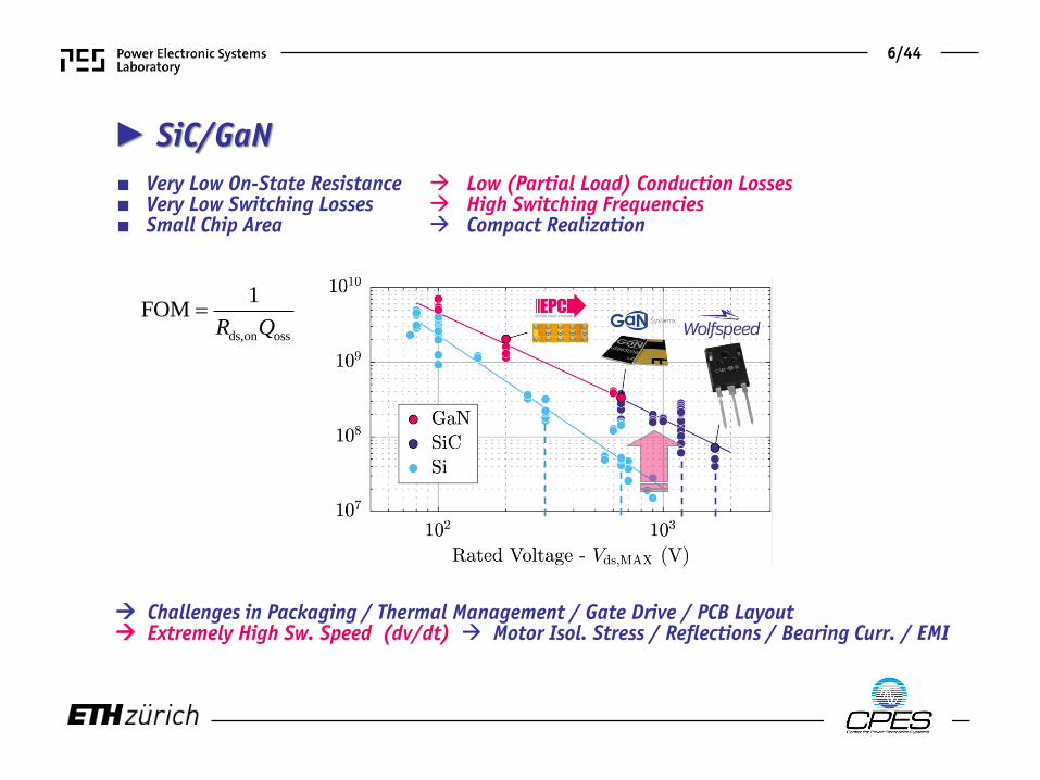
► SiC/GaN
Challenges in Packaging / Thermal Management / Gate Drive / PCB Layout Extremely High Sw. Speed (dv/dt) Motor Isol. Stress / Reflections / Bearing Curr. / EMI
■ Very Low On-State Resistance Low (Partial Load) Conduction Losses ■ Very Low Switching Losses High Switching Frequencies■ Small Chip Area Compact Realization
6/44
ds,on oss
1FOM
R Q
7/44
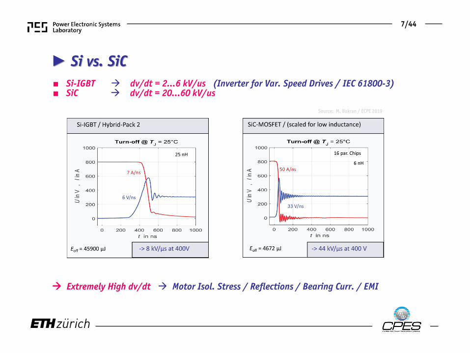
Source: M. Bakran / ECPE 2019
► Si vs. SiC
Extremely High dv/dt Motor Isol. Stress / Reflections / Bearing Curr. / EMI
■ Si-IGBT dv/dt = 2…6 kV/us (Inverter for Var. Speed Drives / IEC 61800-3) ■ SiC dv/dt = 20…60 kV/us
dv/dt - Challenges
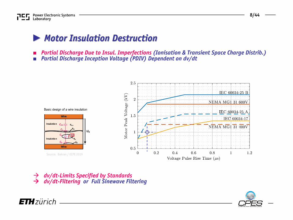
► Motor Insulation Destruction
dv/dt-Limits Specified by Standards dv/dt-Filtering or Full Sinewave Filtering
■ Partial Discharge Due to Insul. Imperfections (Ionisation & Transient Space Charge Distrib.) ■ Partial Discharge Inception Voltage (PDIV) Dependent on dv/dt
8/44
Source: Bakran / ECPE 2019
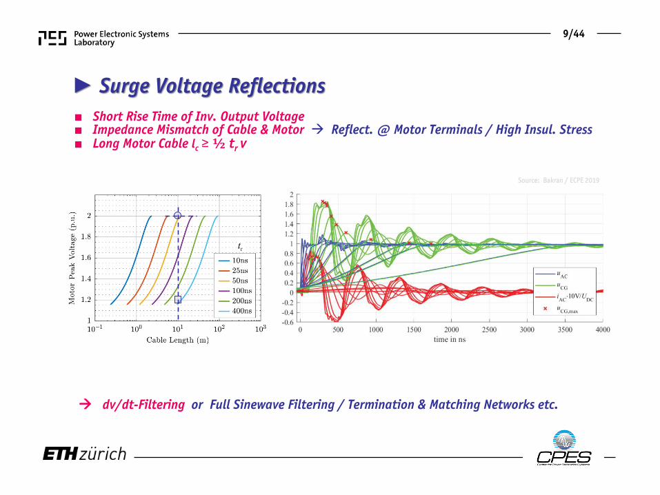
► Surge Voltage Reflections■ Short Rise Time of Inv. Output Voltage ■ Impedance Mismatch of Cable & Motor Reflect. @ Motor Terminals / High Insul. Stress■ Long Motor Cable lc ≥ ½ tr v
9/44
Source: Bakran / ECPE 2019
dv/dt-Filtering or Full Sinewave Filtering / Termination & Matching Networks etc.
10/44
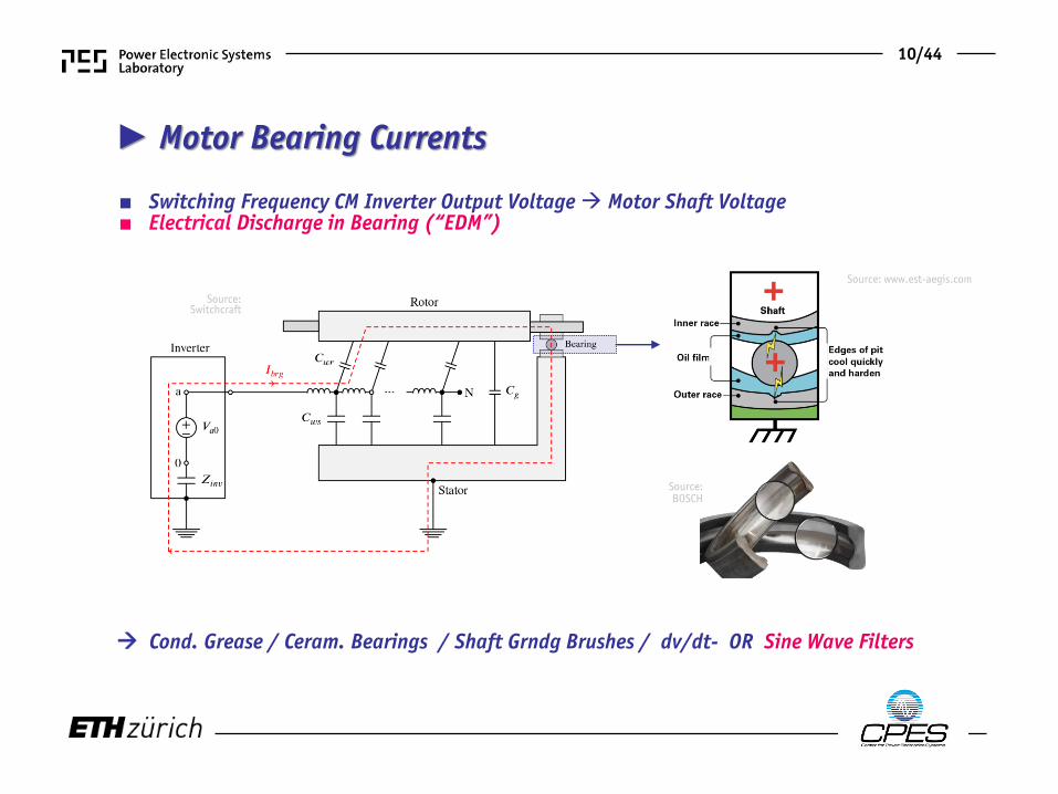
■ Switching Frequency CM Inverter Output Voltage Motor Shaft Voltage■ Electrical Discharge in Bearing (“EDM”)
Cond. Grease / Ceram. Bearings / Shaft Grndg Brushes / dv/dt- OR Sine Wave Filters
Source: Switchcraft
Source: BOSCH
► Motor Bearing Currents
Source: www.est-aegis.com
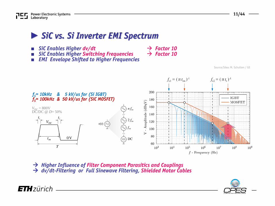
► SiC vs. Si Inverter EMI Spectrum ■ SiC Enables Higher dv/dt Factor 10■ SiC Enables Higher Switching Frequencies Factor 10 ■ EMI Envelope Shifted to Higher Frequencies
Higher Influence of Filter Component Parasitics and Couplings dv/dt-Filtering or Full Sinewave Filtering, Shielded Motor Cables
11/44
fS= 10kHz & 5 kV/us for (Si IGBT)fS= 100kHz & 50 kV/us for (SiC MOSFET)
VDC = 800VDC/DC @ D= 50%
Source/Idea: M. Schutten / GE
● EMI Standards (Cond. & Rad.) Shielded Motor Cables OR Full Sinewave Filtering
12/44
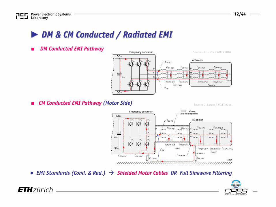
► DM & CM Conducted / Radiated EMI ■ DM Conducted EMI Pathway
Source: J. Luszcz / WILEY 2018
■ CM Conducted EMI Pathway (Motor Side) Source: J. Luszcz / WILEY 2018
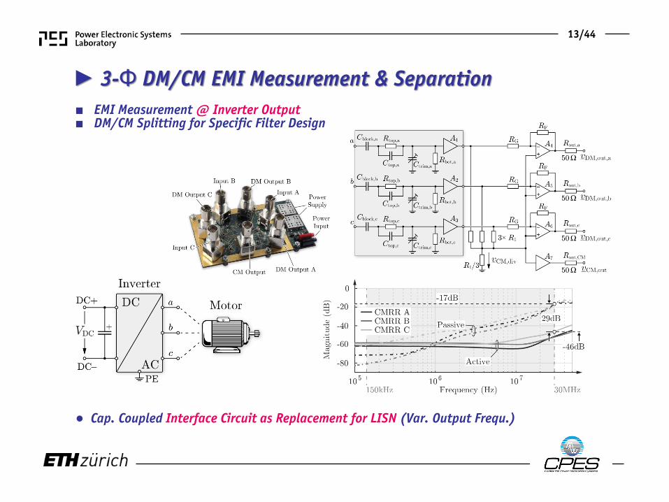
► 3-Φ DM/CM EMI Measurement & Separation■ EMI Measurement @ Inverter Output ■ DM/CM Splitting for Specific Filter Design
● Cap. Coupled Interface Circuit as Replacement for LISN (Var. Output Frequ.)
13/44
dv/dt-FiltersMotor Cable Termination
Staggered SwitchingActive CM Filtering
Inverter Output Filters
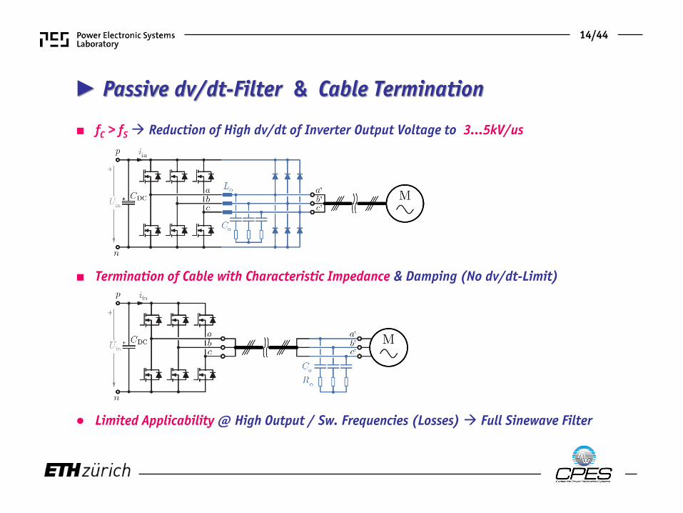
► Passive dv/dt-Filter & Cable Termination
● Limited Applicability @ High Output / Sw. Frequencies (Losses) Full Sinewave Filter
■ fC > fS Reduction of High dv/dt of Inverter Output Voltage to 3…5kV/us
14/44
■ Termination of Cable with Characteristic Impedance & Damping (No dv/dt-Limit)
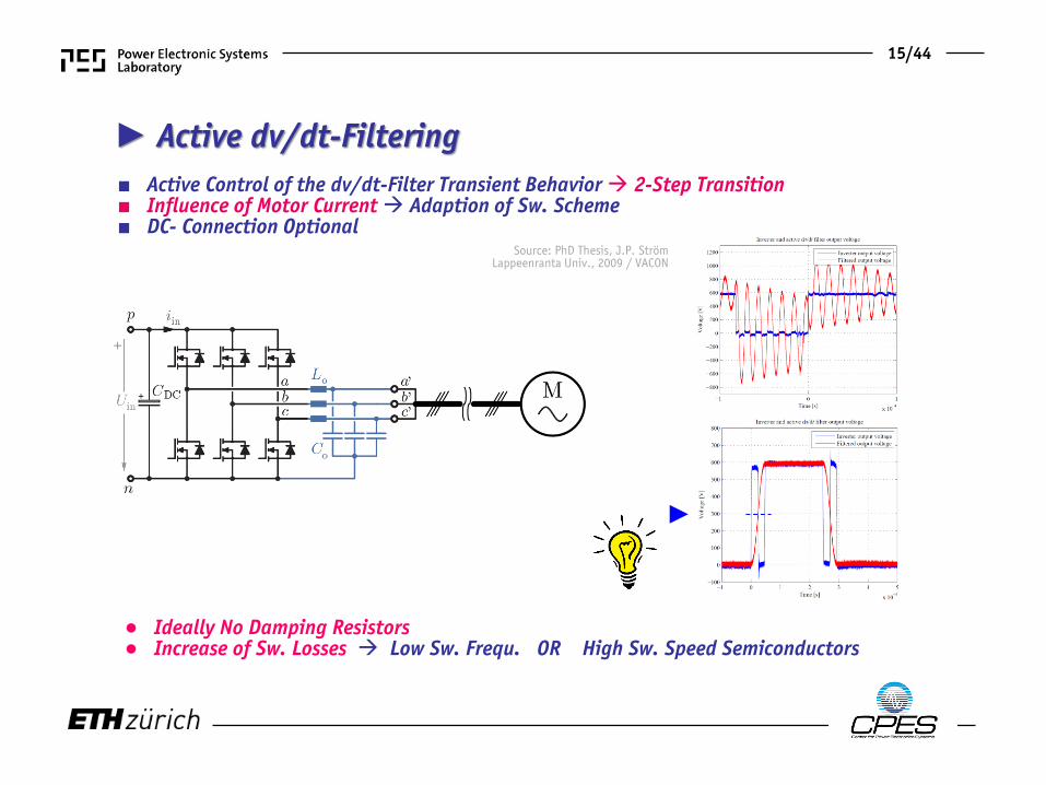
► Active dv/dt-Filtering
● Ideally No Damping Resistors ● Increase of Sw. Losses Low Sw. Frequ. OR High Sw. Speed Semiconductors
■ Active Control of the dv/dt-Filter Transient Behavior 2-Step Transition■ Influence of Motor Current Adaption of Sw. Scheme■ DC- Connection Optional
15/44
►
Source: PhD Thesis, J.P. StrömLappeenranta Univ., 2009 / VACON
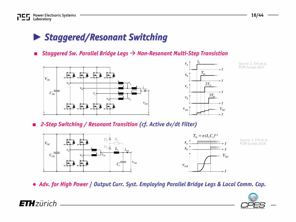
► Staggered/Resonant Switching
● Adv. for High Power / Output Curr. Syst. Employing Parallel Bridge Legs & Local Comm. Cap.
16/44
■ 2-Step Switching / Resonant Transition (cf. Active dv/dt Filter)
■ Staggered Sw. Parallel Bridge Legs Non-Resonant Multi-Step Transistion
Source: J. Ertl et al.PCIM Europe 2017
Source: J. Ertl et al.PCIM Europe 2018
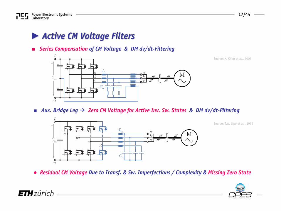
► Active CM Voltage Filters
● Residual CM Voltage Due to Transf. & Sw. Imperfections / Complexity & Missing Zero State
■ Series Compensation of CM Voltage & DM dv/dt-Filtering
17/44
■ Aux. Bridge Leg Zero CM Voltage for Active Inv. Sw. States & DM dv/dt-Filtering
Source: X. Chen et al., 2007
Source: T.A. Lipo et al., 1999
Sinewave Filters
Inverter Output Filters
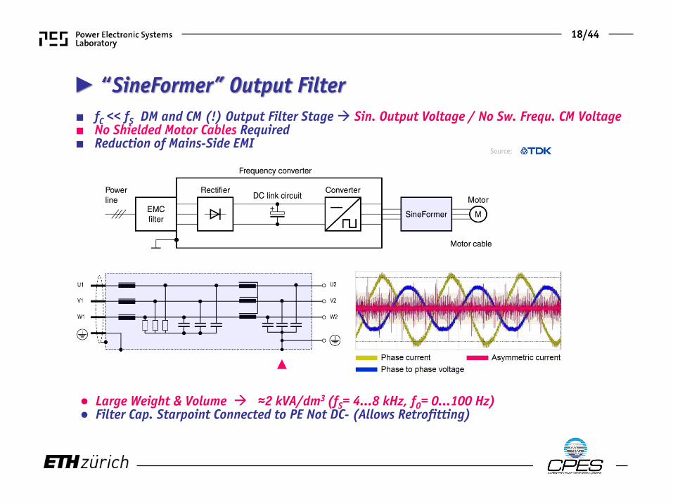
► “SineFormer” Output Filter
● Large Weight & Volume ≈2 kVA/dm3 (fS= 4…8 kHz, fO= 0…100 Hz)● Filter Cap. Starpoint Connected to PE Not DC- (Allows Retrofitting)
■ fC << fS DM and CM (!) Output Filter Stage Sin. Output Voltage / No Sw. Frequ. CM Voltage■ No Shielded Motor Cables Required■ Reduction of Mains-Side EMI
18/44
Source:
▲
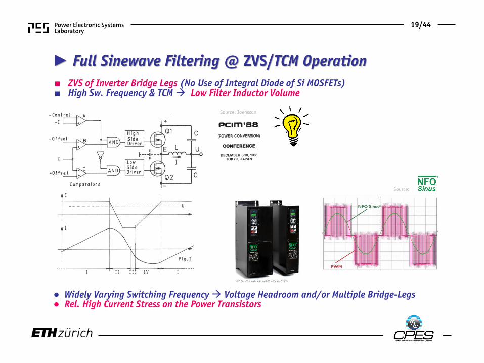
► Full Sinewave Filtering @ ZVS/TCM Operation
● Widely Varying Switching Frequency Voltage Headroom and/or Multiple Bridge-Legs● Rel. High Current Stress on the Power Transistors
■ ZVS of Inverter Bridge Legs (No Use of Integral Diode of Si MOSFETs)■ High Sw. Frequency & TCM Low Filter Inductor Volume
19/44
Source: Joensson
Source:
● GTHM — Results in Add. Cap. Reactive Power Limited for Higher Frequencies
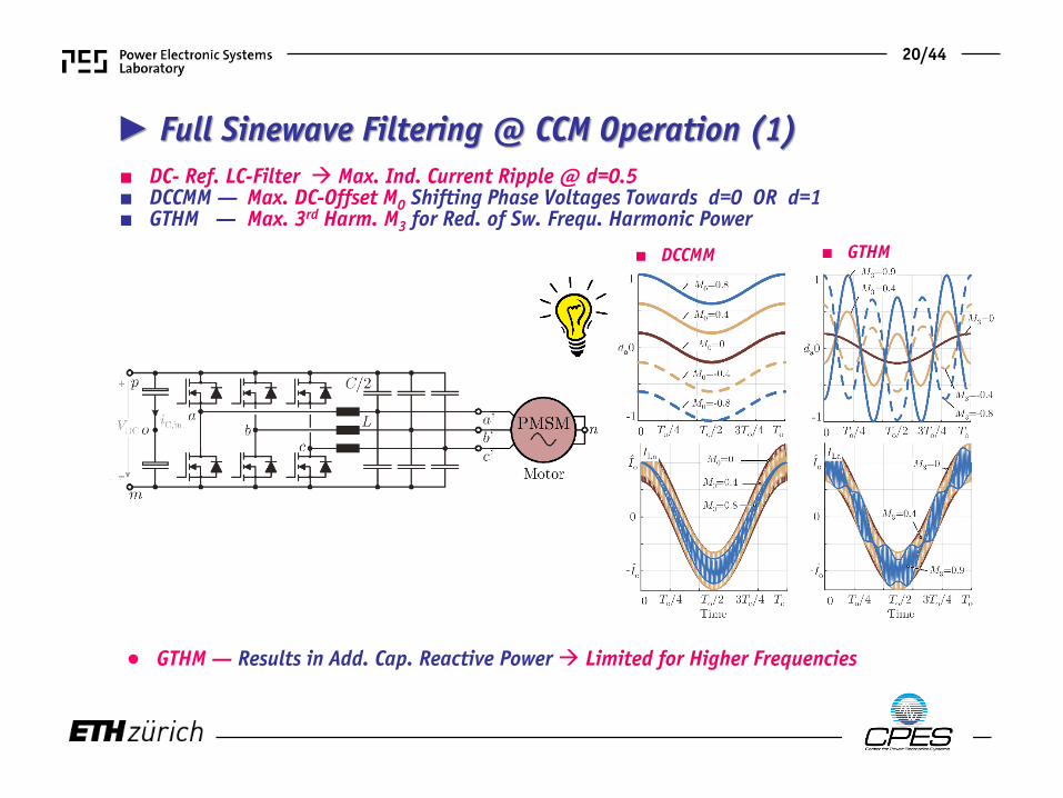
■ DC- Ref. LC-Filter Max. Ind. Current Ripple @ d=0.5■ DCCMM — Max. DC-Offset M0 Shifting Phase Voltages Towards d=0 OR d=1■ GTHM — Max. 3rd Harm. M3 for Red. of Sw. Frequ. Harmonic Power
► Full Sinewave Filtering @ CCM Operation (1)
20/44
■ DCCMM ■ GTHM
21/44
● GTHM — Results in Add. Cap. Reactive Power Limited for Higher Frequencies
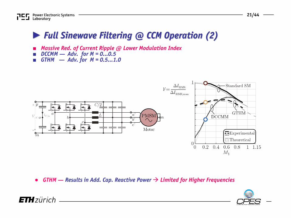
■ Massive Red. of Current Ripple @ Lower Modulation Index■ DCCMM — Adv. for M = 0…0.5 ■ GTHM — Adv. for M = 0.5…1.0
► Full Sinewave Filtering @ CCM Operation (2)
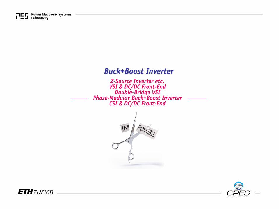
Z-Source Inverter etc.VSI & DC/DC Front-End
Double-Bridge VSIPhase-Modular Buck+Boost Inverter
CSI & DC/DC Front-End
Buck+Boost Inverter
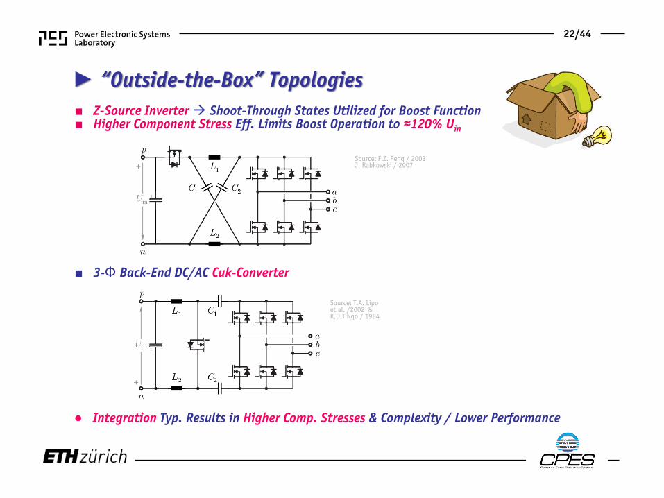
● Integration Typ. Results in Higher Comp. Stresses & Complexity / Lower Performance
■ Z-Source Inverter Shoot-Through States Utilized for Boost Function■ Higher Component Stress Eff. Limits Boost Operation to ≈120% Uin
► “Outside-the-Box” Topologies
22/44
■ 3-Φ Back-End DC/AC Cuk-Converter
Source: F.Z. Peng / 2003J. Rabkowski / 2007
Source: T.A. Lipo et al. /2002 &K.D.T Ngo / 1984
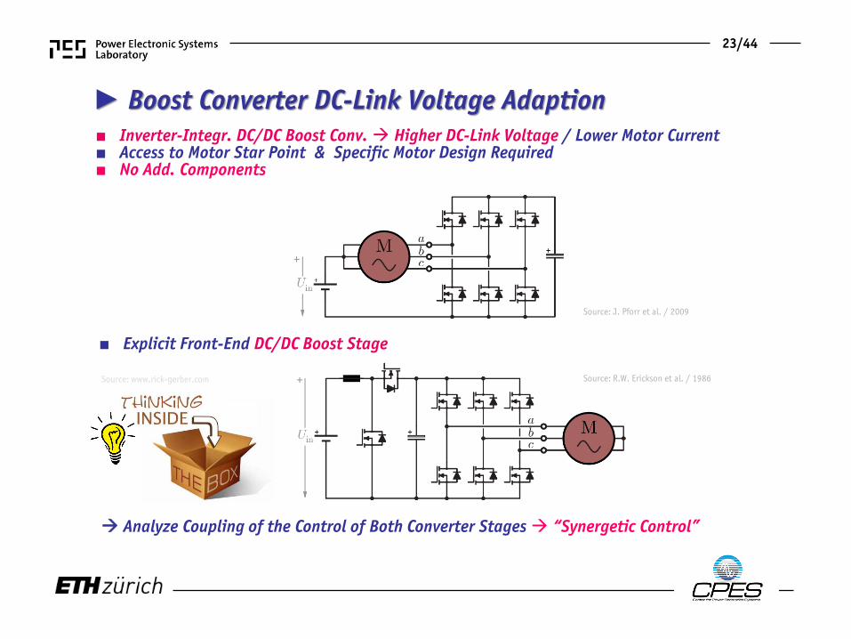
Analyze Coupling of the Control of Both Converter Stages “Synergetic Control”
► Boost Converter DC-Link Voltage Adaption
23/44
Source: www.rick-gerber.com
■ Inverter-Integr. DC/DC Boost Conv. Higher DC-Link Voltage / Lower Motor Current■ Access to Motor Star Point & Specific Motor Design Required■ No Add. Components
■ Explicit Front-End DC/DC Boost Stage
Source: J. Pforr et al. / 2009
Source: R.W. Erickson et al. / 1986
● Preferable for Low Dynamics Drive Systems
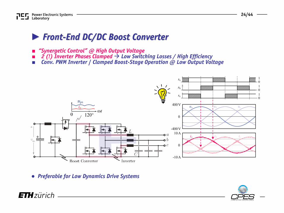
■ “Synergetic Control” @ High Output Voltage ■ 2 (!) Inverter Phases Clamped Low Switching Losses / High Efficiency■ Conv. PWM Inverter / Clamped Boost-Stage Operation @ Low Output Voltage
► Front-End DC/DC Boost Converter
24/44
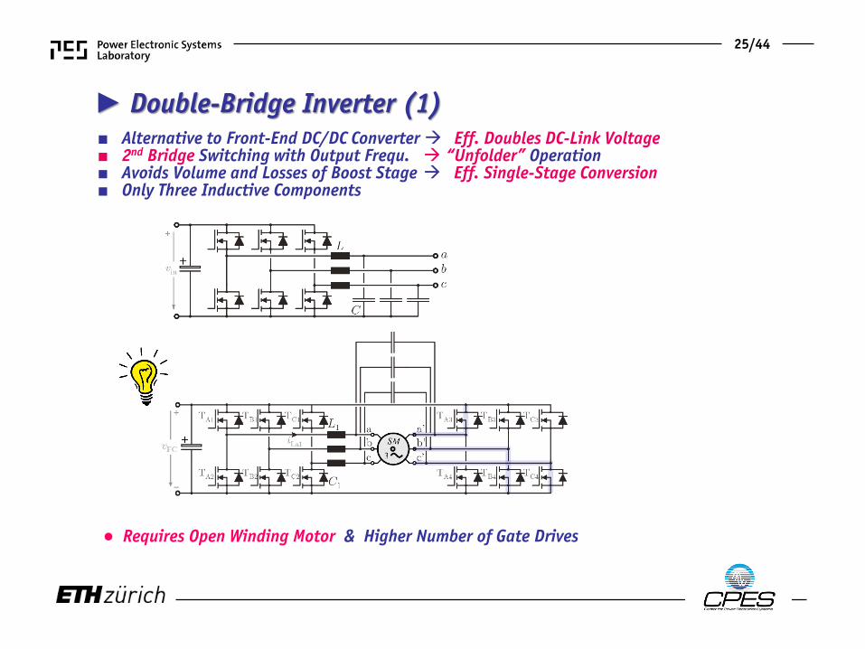
● Requires Open Winding Motor & Higher Number of Gate Drives
■ Alternative to Front-End DC/DC Converter Eff. Doubles DC-Link Voltage■ 2nd Bridge Switching with Output Frequ. “Unfolder” Operation■ Avoids Volume and Losses of Boost Stage Eff. Single-Stage Conversion■ Only Three Inductive Components
► Double-Bridge Inverter (1)
25/44
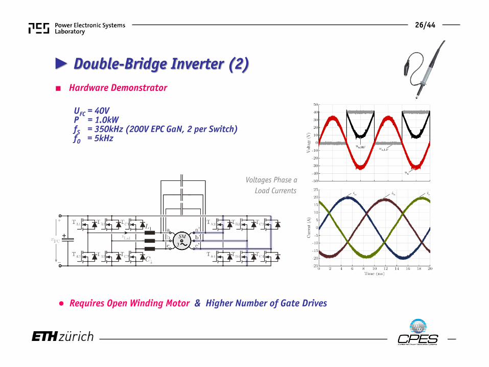
■ Hardware Demonstrator
Voltages Phase aLoad Currents
26/44
► Double-Bridge Inverter (2)
UFC = 40VP = 1.0kWfS = 350kHz (200V EPC GaN, 2 per Switch)fO = 5kHz
● Requires Open Winding Motor & Higher Number of Gate Drives
27/44
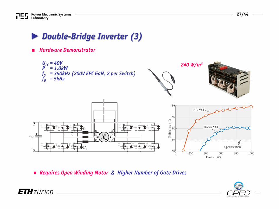
240 W/in3
■ Hardware Demonstrator
► Double-Bridge Inverter (3)
UFC = 40VP = 1.0kWfS = 350kHz (200V EPC GaN, 2 per Switch)fO = 5kHz
● Requires Open Winding Motor & Higher Number of Gate Drives
Specification
Boost+Buck ModulesBuck+Boost Modules
Phase-Modular Topologies
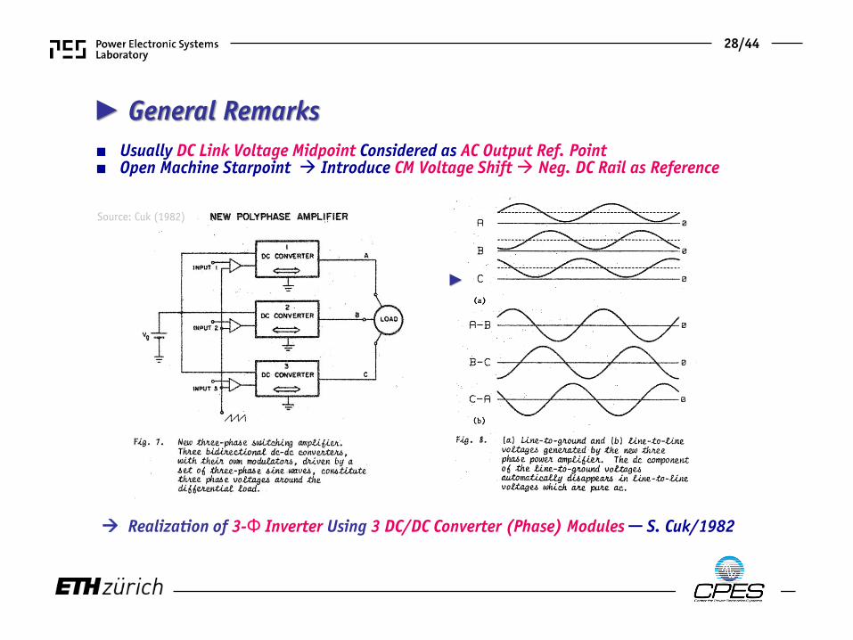
Realization of 3-Φ Inverter Using 3 DC/DC Converter (Phase) Modules ─ S. Cuk/1982
■ Usually DC Link Voltage Midpoint Considered as AC Output Ref. Point ■ Open Machine Starpoint Introduce CM Voltage Shift Neg. DC Rail as Reference
► General Remarks
28/44
Source: Cuk (1982)
►
29/44
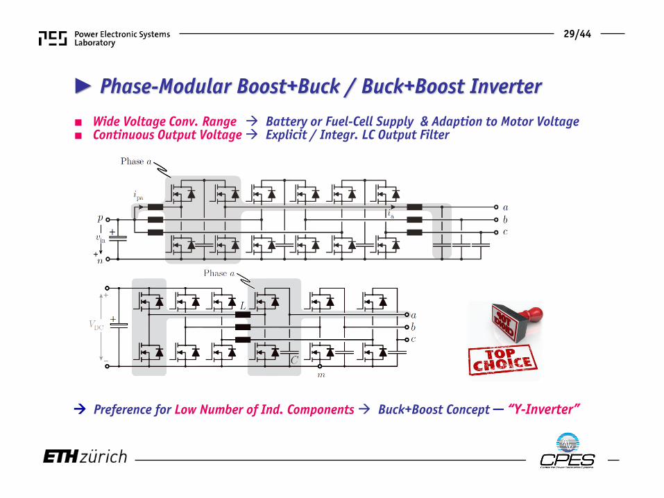
■ Wide Voltage Conv. Range Battery or Fuel-Cell Supply & Adaption to Motor Voltage■ Continuous Output Voltage Explicit / Integr. LC Output Filter
Preference for Low Number of Ind. Components Buck+Boost Concept ─ “Y-Inverter”
► Phase-Modular Boost+Buck / Buck+Boost Inverter
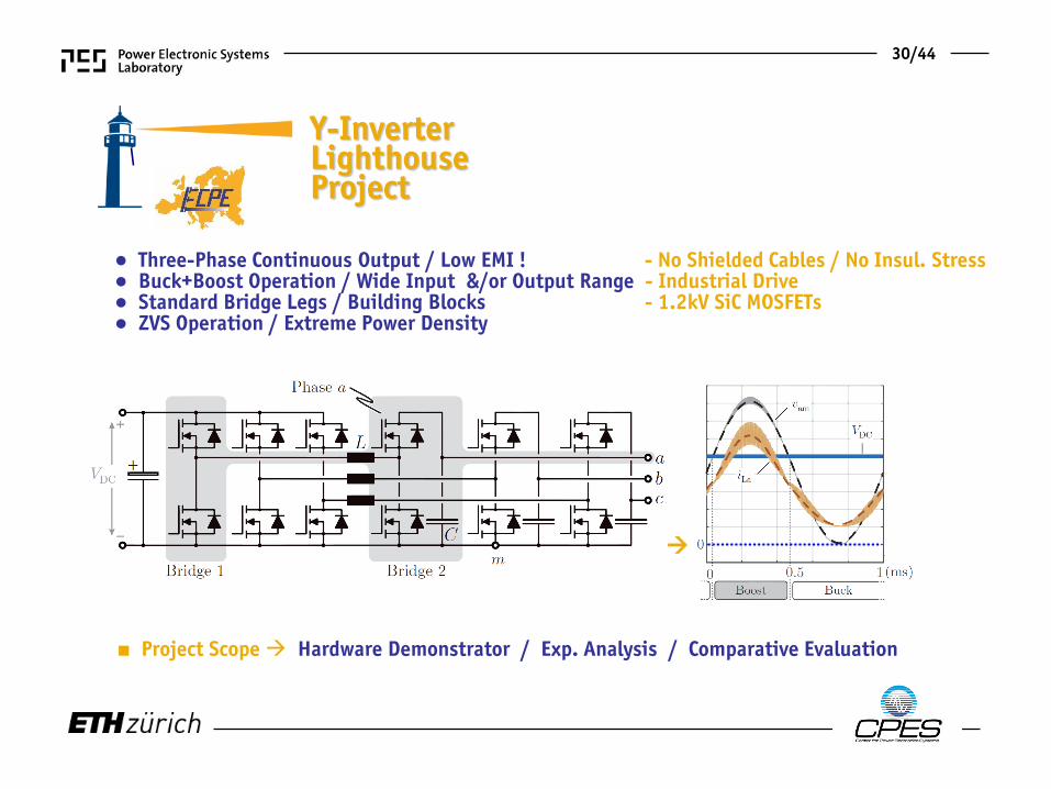
■ Project Scope Hardware Demonstrator / Exp. Analysis / Comparative Evaluation
● Three-Phase Continuous Output / Low EMI ! - No Shielded Cables / No Insul. Stress● Buck+Boost Operation / Wide Input &/or Output Range - Industrial Drive● Standard Bridge Legs / Building Blocks - 1.2kV SiC MOSFETs● ZVS Operation / Extreme Power Density
30/44
Y-InverterLighthouseProject
31/44
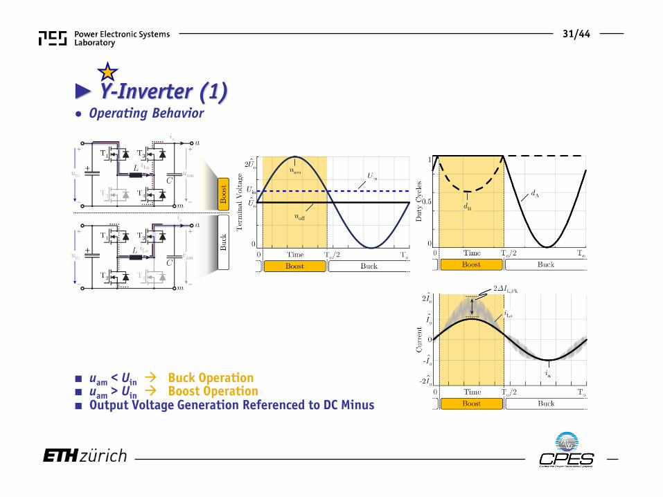
● Operating Behavior► Y-Inverter (1)
■ uam < Uin Buck Operation■ uam > Uin Boost Operation ■ Output Voltage Generation Referenced to DC Minus
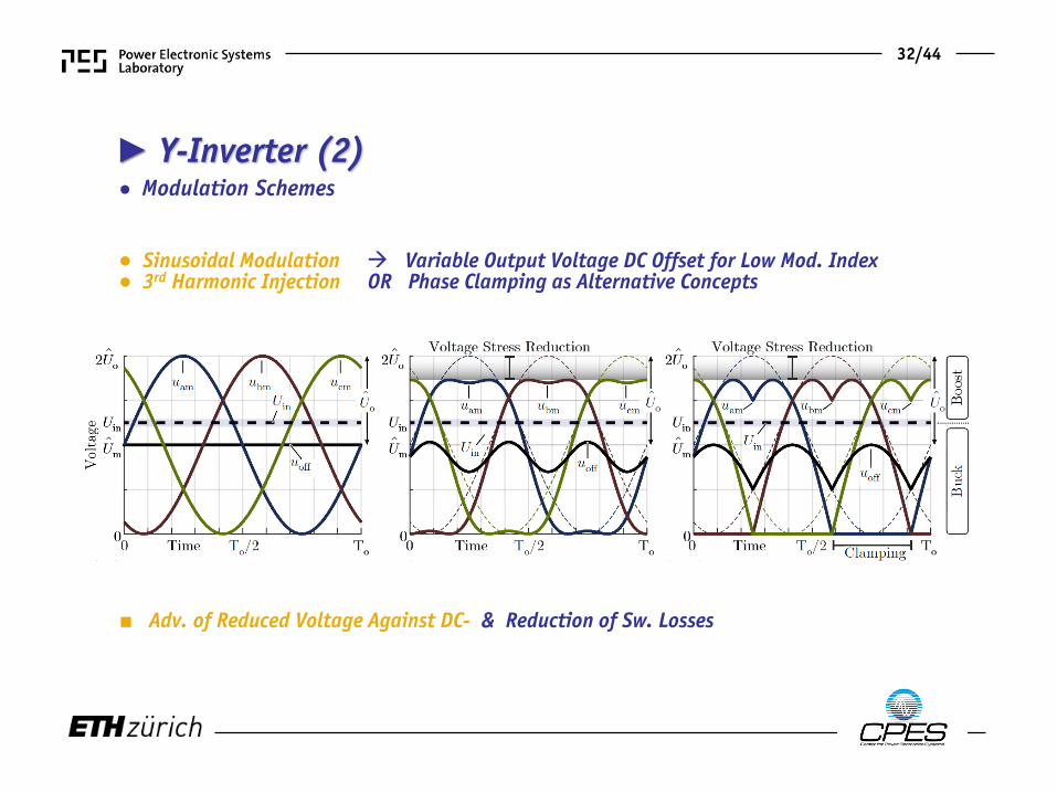
■ Adv. of Reduced Voltage Against DC- & Reduction of Sw. Losses
● Modulation Schemes
32/44
● Sinusoidal Modulation Variable Output Voltage DC Offset for Low Mod. Index● 3rd Harmonic Injection OR Phase Clamping as Alternative Concepts
► Y-Inverter (2)
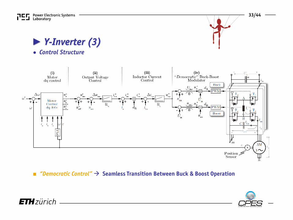
■ “Democratic Control” Seamless Transition Between Buck & Boost Operation
33/44
● Control Structure► Y-Inverter (3)
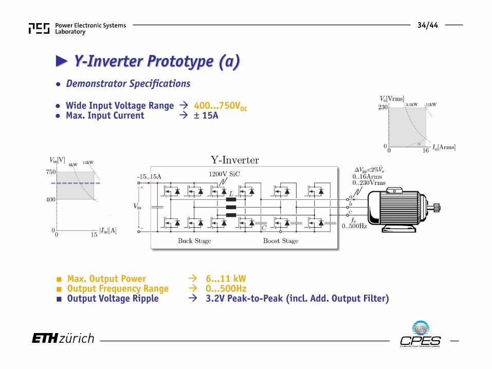
■ Max. Output Power 6…11 kW■ Output Frequency Range 0…500Hz■ Output Voltage Ripple 3.2V Peak-to-Peak (incl. Add. Output Filter)
● Wide Input Voltage Range 400…750VDC● Max. Input Current ± 15A
34/44
● Demonstrator Specifications
► Y-Inverter Prototype (a)
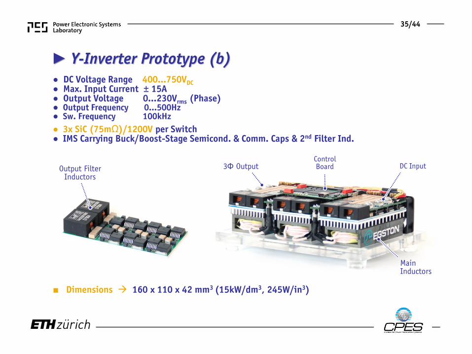
■ Dimensions 160 x 110 x 42 mm3 (15kW/dm3, 245W/in3)
Control Board
35/44
► Y-Inverter Prototype (b)
Main Inductors
3Φ Output
● DC Voltage Range 400…750VDC● Max. Input Current ± 15A● Output Voltage 0…230Vrms (Phase)● Output Frequency 0…500Hz● Sw. Frequency 100kHz● 3x SiC (75mΩ)/1200V per Switch ● IMS Carrying Buck/Boost-Stage Semicond. & Comm. Caps & 2nd Filter Ind.
Output FilterInductors
DC Input
36/44
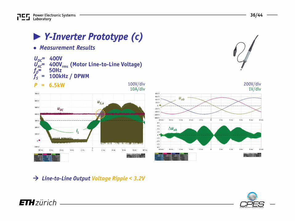
Line-to-Line Output Voltage Ripple < 3.2V
► Y-Inverter Prototype (c)
100V/div10A/div
● Measurement Results
uDC
iL
uS,a
200V/div1V/div
uab
∆uab
UDC= 400VUAC= 400Vrms (Motor Line-to-Line Voltage) fO= 50HzfS = 100kHz / DPWMP = 6.5kW
Multi-Level Bridge Leg Structure for Ind. Comp. Volume Reduction
37/44
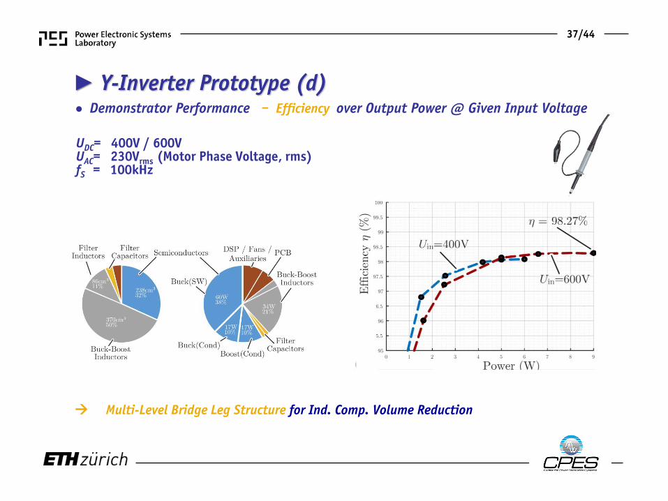
► Y-Inverter Prototype (d)● Demonstrator Performance – Efficiency over Output Power @ Given Input Voltage
UDC= 400V / 600VUAC= 230Vrms (Motor Phase Voltage, rms)fS = 100kHz
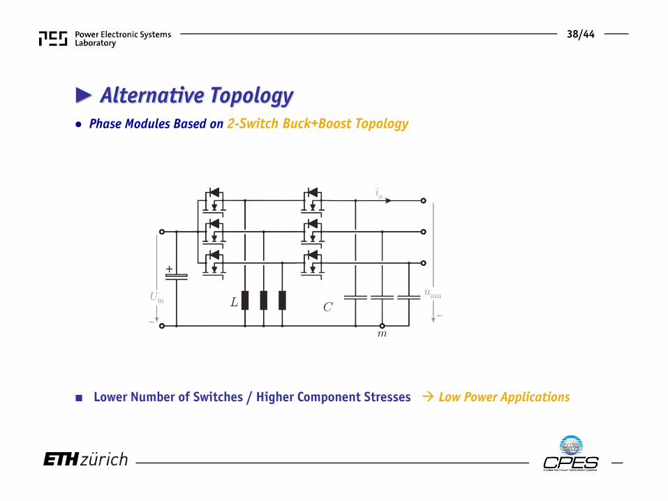
■ Lower Number of Switches / Higher Component Stresses Low Power Applications
38/44
● Phase Modules Based on 2-Switch Buck+Boost Topology
► Alternative Topology
Monolithic Bidir. GaN SwitchesSynergetic Control
DC/DC Buck Stage &Current Source Inverter
39/44
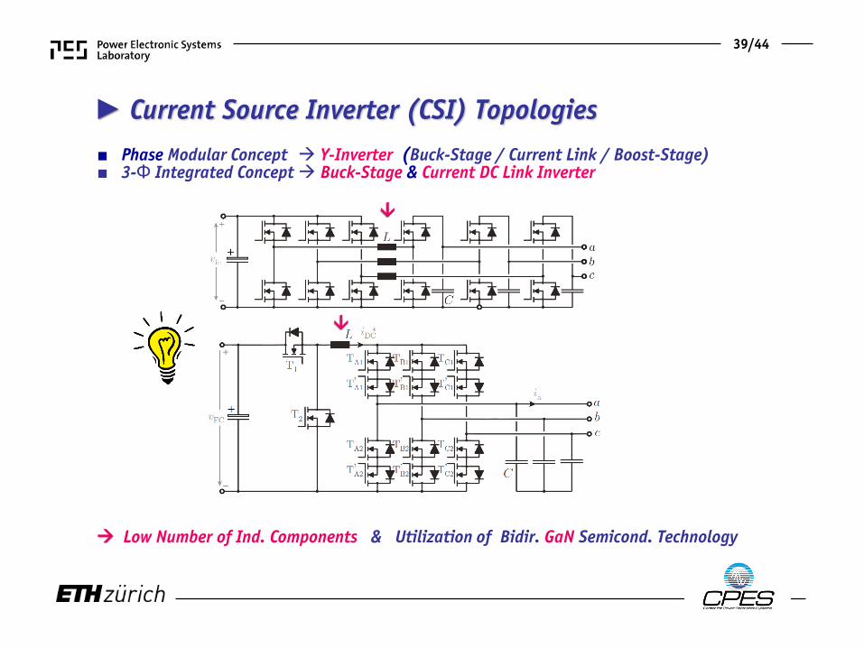
► Current Source Inverter (CSI) Topologies■ Phase Modular Concept Y-Inverter (Buck-Stage / Current Link / Boost-Stage) ■ 3-Φ Integrated Concept Buck-Stage & Current DC Link Inverter
Low Number of Ind. Components & Utilization of Bidir. GaN Semicond. Technology
40/44
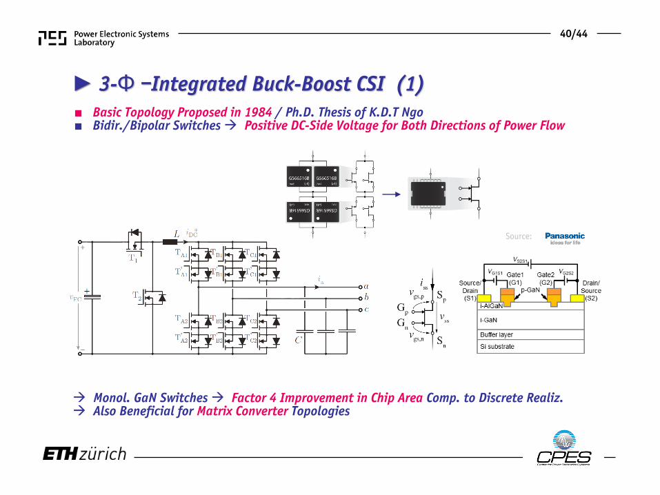
■ Basic Topology Proposed in 1984 / Ph.D. Thesis of K.D.T Ngo ■ Bidir./Bipolar Switches Positive DC-Side Voltage for Both Directions of Power Flow
Monol. GaN Switches Factor 4 Improvement in Chip Area Comp. to Discrete Realiz. Also Beneficial for Matrix Converter Topologies
► 3-Φ –Integrated Buck-Boost CSI (1)
Source:
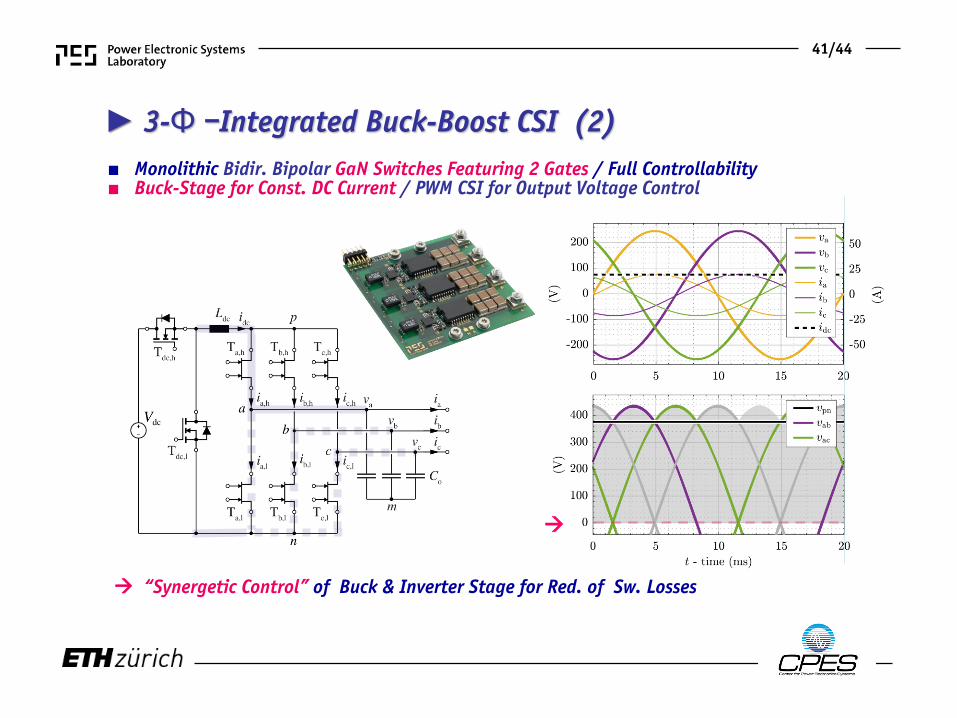
“Synergetic Control” of Buck & Inverter Stage for Red. of Sw. Losses
■ Monolithic Bidir. Bipolar GaN Switches Featuring 2 Gates / Full Controllability ■ Buck-Stage for Const. DC Current / PWM CSI for Output Voltage Control
41/44
► 3-Φ –Integrated Buck-Boost CSI (2)
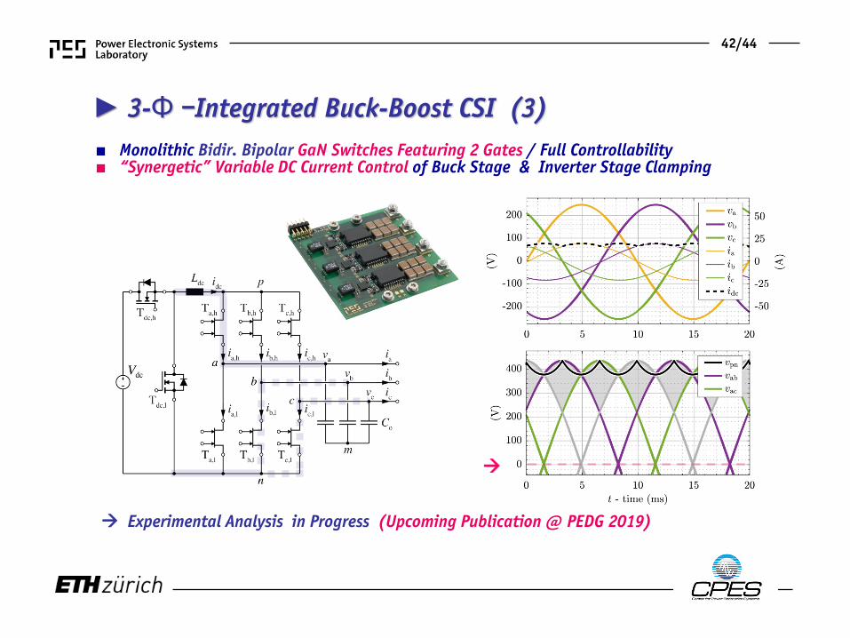
Experimental Analysis in Progress (Upcoming Publication @ PEDG 2019)
42/44
■ Monolithic Bidir. Bipolar GaN Switches Featuring 2 Gates / Full Controllability ■ “Synergetic” Variable DC Current Control of Buck Stage & Inverter Stage Clamping
► 3-Φ –Integrated Buck-Boost CSI (3)
Integrated Modular Motor Drive
Further Concepts
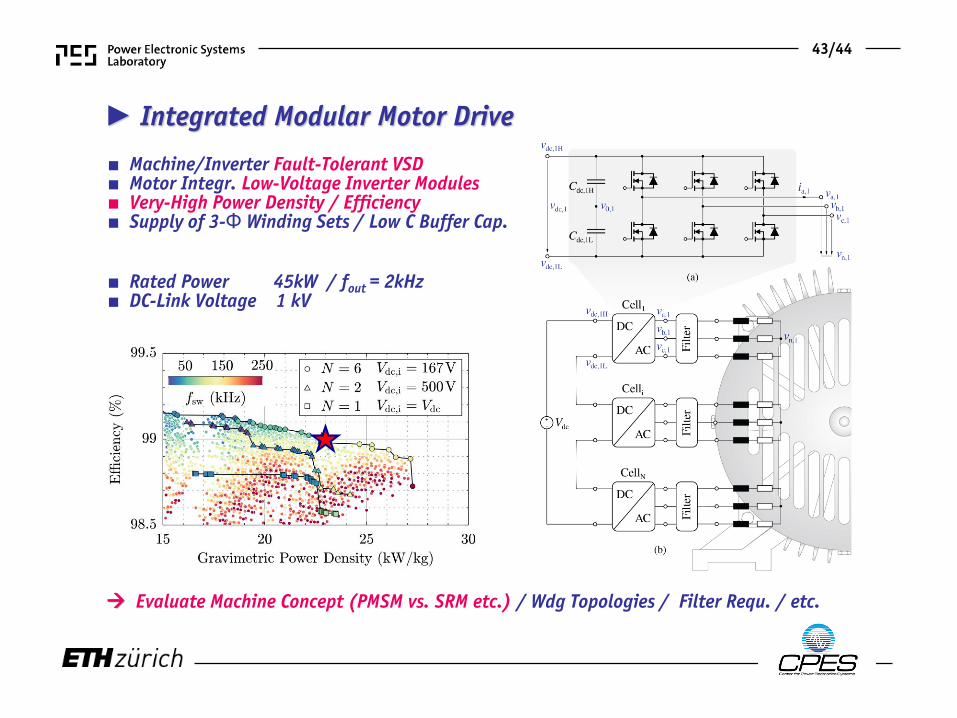
► Integrated Modular Motor Drive
■ Machine/Inverter Fault-Tolerant VSD■ Motor Integr. Low-Voltage Inverter Modules■ Very-High Power Density / Efficiency■ Supply of 3-Φ Winding Sets / Low C Buffer Cap.
43/44
■ Rated Power 45kW / fout = 2kHz■ DC-Link Voltage 1 kV
Evaluate Machine Concept (PMSM vs. SRM etc.) / Wdg Topologies / Filter Requ. / etc.
Conclusions
■ System Level Integr. of Storage, Distrib. DC Bus, Hybrid Hydr./Pneum./El. Drives etc.
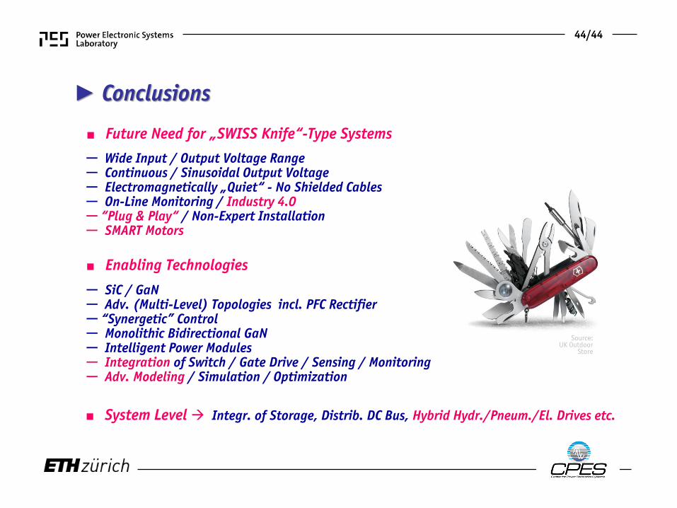
► Conclusions
44/44
■ Enabling Technologies
─ SiC / GaN─ Adv. (Multi-Level) Topologies incl. PFC Rectifier─ “Synergetic” Control─ Monolithic Bidirectional GaN─ Intelligent Power Modules─ Integration of Switch / Gate Drive / Sensing / Monitoring ─ Adv. Modeling / Simulation / Optimization
■ Future Need for „SWISS Knife“-Type Systems
─ Wide Input / Output Voltage Range─ Continuous / Sinusoidal Output Voltage─ Electromagnetically „Quiet“ - No Shielded Cables─ On-Line Monitoring / Industry 4.0─ “Plug & Play“ / Non-Expert Installation─ SMART Motors
Source: UK Outdoor
Store
Thank You !