A 20μW 95dB DR Single-Bit Delta-Sigma Modulator for Portable
6
A 20μW 95dB DR Single-Bit Delta-Sigma Modulator for Portable Measurement Applications Jian Xu, Hanqing Wang, Xiaobo Wu † Abstract–A low power high performance Delta-Sigma mod- ulator for portable measurement applications is presented in this paper. To reduce the power consumption and ensure high performance, a comprehensive system-level design adopting a new method to determine the DC gain value of Operational Transconductance Amplifier (OTA) and considering the effect of 1/f noise is introduced. Besides, a novel power efficient cur- rent mirror Class-AB OTA with a fast-settling less-error switched-capacitor common-mode feedback (SC CMFB) cir- cuit is proposed in this design. And the bottom terminal para- sitic-effect of Poly-Insulator-Poly (PIP) capacitors is also con- sidered. Therefore, about extra 20% of the capacitance is add- ed to the total capacitance load. In addition, an area-efficient power-efficient resonator is adopted to realize a coefficient of 1/90 for 50% power and 75% area cost reduction over the conventional design. The chip is implemented in a low cost standard 0.35μm CMOS. Its total power is only 20μW at a 1.5V supply, and the measured Dynamic Range (DR) is 95dB over the 1 kHz bandwidth. The designed modulator shows very high Figure-of-Merit (FOM) among the recent low power high per- formance modulators. Keywords–low power, high performance, Delta-Sigma mod- ulator, switched capacitor circuits I. INTRODUCTION Recently, portable electronic devices, such as portable measurement, implantable medical devices and digital cam- eras, were greatly demanded in the consumer market [1]. Low power is of great importance for these battery-powered devices to increase the battery lifetime. Hence, more power efficient circuits have been demanded than ever [2]. As an important building block, Delta-Sigma modulators are widely used in these portable devices. Therefore, the design of low power high performance modulators is essential to these devices. The improvement of low power high performance mod- ulators has been continuing to develop [1]-[8]. Utilization of an advanced CMOS process with a low threshold voltage is a common method, but its cost is high [1], [2]. Some works were implemented with a switched-opamp (SO) technique, which can reduce both the power and supply voltage [4], [5]. However, the power efficiency of the SOs used in these works is not high. Considering the OTA itself, a body-driven technique was also used to reduce both the supply voltage and power consumption [6]. The drawback is that the body- driven transistors have some limitations caused by bad noise performance [7]. To remove the need of OTAs, comparator- based and inverter-based SC circuits have been proposed in [3], [8]. Both two techniques have the ability to operate with low supply voltage and power consumption. However, it is difficult for these two techniques to realize a resolution up to 14-bit or more due to the residual offset and stringent conditions for the required operation region. Jian Xu, Hanqing Wang and Xiaobo Wu † are with the Institute of VLSI Design, Zhejiang University, Hangzhou, China (corresponding author to provide phone: 86-0571-8795-2666; email: [email protected]) To reduce the cost of chip fabrication, this paper focuses on the design in a low cost 0.35μm CMOS. Through the comprehensive system-level design and the use of novel power efficient OTA and resonator, the proposed modulator in this paper can also achieve low power and high perfor- mance without needing an advanced or special process. Section II discusses the details of system-level design for low power high performance applications. A new method to determine the DC gain values of OTAs and the effect of 1/f noise are introduced. Then, section III shows the main cir- cuit building blocks design. A novel power efficient OTA and an area-efficient power-efficient small-coefficient reso- nator are adopted in this design. The measurement and con- clusion are given in Section IV and Section V, respectively. II. SYSTEM LEVEL DESIGN A. Modulator Topology Fig.1. Single-loop 4th-order modulator topology. The proposed 4th-order modulator topology with OSR= 64 is shown in Fig.1. Single-loop topology is preferable for low voltage low power applications because it is more in- sensitive to analog circuit non-idealities, such as OTA DC gain, switch on-resistance and so on [1]. Also, a fully feed- forward architecture widely used in recent years is adopted [1], [9]. This feedforward architecture has extra signal paths from the outputs of the integrators to the quantizer, so most signal energy can be prevented from leaking into the loop. The design requirements of the OTAs can be relaxed, and the power consumption can be also reduced greatly. Al- though single-loop multi-bit modulator topology can allow lower power with a lower OSR, it is hard to realize a feed- back Digital-to-Analog Converter (DAC) with a linearity much better than 10~12 bits without trimming [10]. Usually, a Dynamic Element Matching (DEM) circuit consuming extra power and area is required to remove the nonlinearity and in-band tones caused by the capacitor-element mis- match of the feedback DAC [10]. Besides, a super low power multi-bit quantizer is difficult to be implemented due to the reference resistor string consuming much extra power and area. Finally, single-loop single-bit modulator architec- ture with inherent linearity was proposed in this paper. The coefficients of the proposed modulator are summa-
Transcript of A 20μW 95dB DR Single-Bit Delta-Sigma Modulator for Portable
A 20μW 95dB DR Single-Bit Delta-Sigma Modulator for Portable Measurement Applications
Jian Xu, Hanqing Wang, Xiaobo Wu† Abstract–A low power high performance Delta-Sigma mod-
ulator for portable measurement applications is presented in this paper. To reduce the power consumption and ensure high performance, a comprehensive system-level design adopting a new method to determine the DC gain value of Operational Transconductance Amplifier (OTA) and considering the effect of 1/f noise is introduced. Besides, a novel power efficient cur-rent mirror Class-AB OTA with a fast-settling less-error switched-capacitor common-mode feedback (SC CMFB) cir-cuit is proposed in this design. And the bottom terminal para-sitic-effect of Poly-Insulator-Poly (PIP) capacitors is also con-sidered. Therefore, about extra 20% of the capacitance is add-ed to the total capacitance load. In addition, an area-efficient power-efficient resonator is adopted to realize a coefficient of 1/90 for 50% power and 75% area cost reduction over the conventional design. The chip is implemented in a low cost standard 0.35μm CMOS. Its total power is only 20μW at a 1.5V supply, and the measured Dynamic Range (DR) is 95dB over the 1 kHz bandwidth. The designed modulator shows very high Figure-of-Merit (FOM) among the recent low power high per-formance modulators.
Keywords–low power, high performance, Delta-Sigma mod-ulator, switched capacitor circuits
I. INTRODUCTION
Recently, portable electronic devices, such as portable measurement, implantable medical devices and digital cam-eras, were greatly demanded in the consumer market [1]. Low power is of great importance for these battery-powered devices to increase the battery lifetime. Hence, more power efficient circuits have been demanded than ever [2]. As an important building block, Delta-Sigma modulators are widely used in these portable devices. Therefore, the design of low power high performance modulators is essential to these devices.
The improvement of low power high performance mod-ulators has been continuing to develop [1]-[8]. Utilization of an advanced CMOS process with a low threshold voltage is a common method, but its cost is high [1], [2]. Some works were implemented with a switched-opamp (SO) technique, which can reduce both the power and supply voltage [4], [5]. However, the power efficiency of the SOs used in these works is not high. Considering the OTA itself, a body-driven technique was also used to reduce both the supply voltage and power consumption [6]. The drawback is that the body- driven transistors have some limitations caused by bad noise performance [7]. To remove the need of OTAs, comparator- based and inverter-based SC circuits have been proposed in [3], [8]. Both two techniques have the ability to operate with low supply voltage and power consumption. However, it is difficult for these two techniques to realize a resolution up to 14-bit or more due to the residual offset and stringent conditions for the required operation region. Jian Xu, Hanqing Wang and Xiaobo Wu† are with the Institute of VLSI Design, Zhejiang University, Hangzhou, China (corresponding author to provide phone: 86-0571-8795-2666; email: [email protected])
To reduce the cost of chip fabrication, this paper focuses on the design in a low cost 0.35μm CMOS. Through the comprehensive system-level design and the use of novel power efficient OTA and resonator, the proposed modulator in this paper can also achieve low power and high perfor-mance without needing an advanced or special process.
Section II discusses the details of system-level design for low power high performance applications. A new method to determine the DC gain values of OTAs and the effect of 1/f noise are introduced. Then, section III shows the main cir-cuit building blocks design. A novel power efficient OTA and an area-efficient power-efficient small-coefficient reso-nator are adopted in this design. The measurement and con-clusion are given in Section IV and Section V, respectively.
II. SYSTEM LEVEL DESIGN
A. Modulator Topology
Fig.1. Single-loop 4th-order modulator topology.
The proposed 4th-order modulator topology with OSR= 64 is shown in Fig.1. Single-loop topology is preferable for low voltage low power applications because it is more in-sensitive to analog circuit non-idealities, such as OTA DC gain, switch on-resistance and so on [1]. Also, a fully feed-forward architecture widely used in recent years is adopted [1], [9]. This feedforward architecture has extra signal paths from the outputs of the integrators to the quantizer, so most signal energy can be prevented from leaking into the loop. The design requirements of the OTAs can be relaxed, and the power consumption can be also reduced greatly. Al-though single-loop multi-bit modulator topology can allow lower power with a lower OSR, it is hard to realize a feed-back Digital-to-Analog Converter (DAC) with a linearity much better than 10~12 bits without trimming [10]. Usually, a Dynamic Element Matching (DEM) circuit consuming extra power and area is required to remove the nonlinearity and in-band tones caused by the capacitor-element mis-match of the feedback DAC [10]. Besides, a super low power multi-bit quantizer is difficult to be implemented due to the reference resistor string consuming much extra power and area. Finally, single-loop single-bit modulator architec-ture with inherent linearity was proposed in this paper.
The coefficients of the proposed modulator are summa-
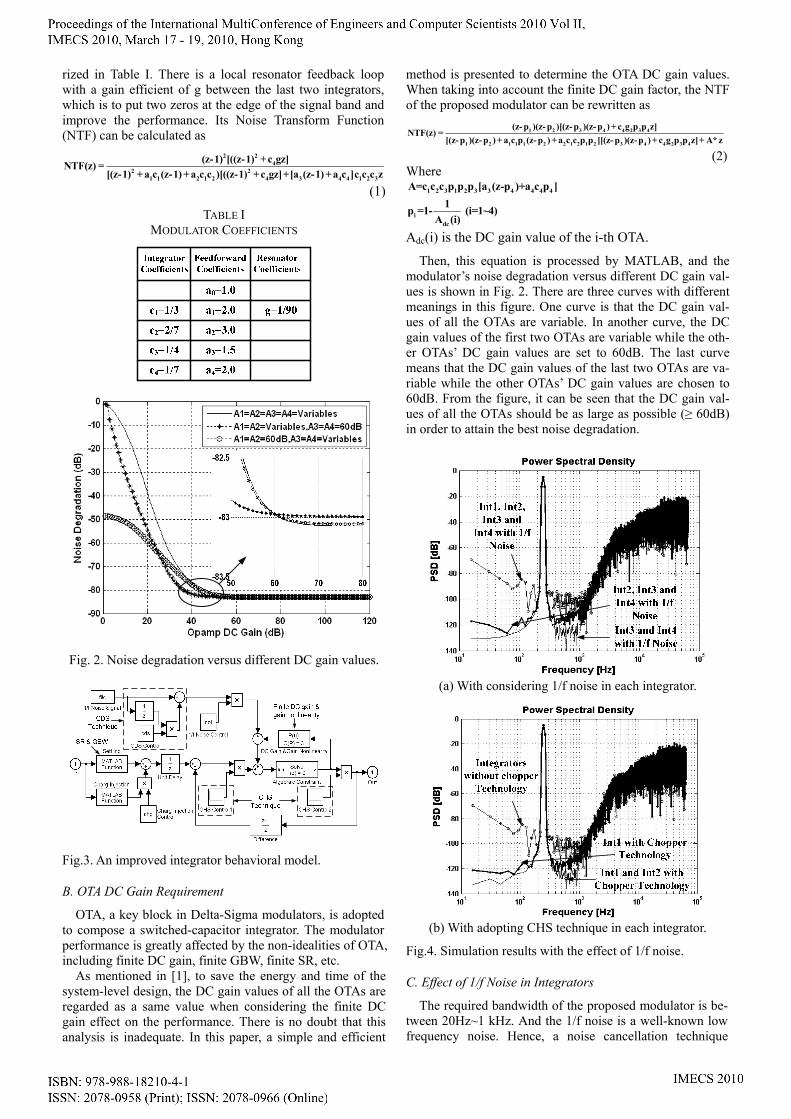
rized in Table I. There is a local resonator feedback loop with a gain efficient of g between the last two integrators, which is to put two zeros at the edge of the signal band and improve the performance. Its Noise Transform Function (NTF) can be calculated as
2 24
2 21 1 2 1 2 4 3 4 4 1 2 3
(z-1) [((z-1) + c gz]NTF(z) =
[(z-1) + a c (z-1) +a c c )[((z-1) + c gz]+[a (z-1) +a c ]c c c z
(1)
TABLE I MODULATOR COEFFICIENTS
Fig. 2. Noise degradation versus different DC gain values.
Fig.3. An improved integrator behavioral model.
B. OTA DC Gain Requirement
OTA, a key block in Delta-Sigma modulators, is adopted to compose a switched-capacitor integrator. The modulator performance is greatly affected by the non-idealities of OTA, including finite DC gain, finite GBW, finite SR, etc.
As mentioned in [1], to save the energy and time of the system-level design, the DC gain values of all the OTAs are regarded as a same value when considering the finite DC gain effect on the performance. There is no doubt that this analysis is inadequate. In this paper, a simple and efficient
method is presented to determine the OTA DC gain values. When taking into account the finite DC gain factor, the NTF of the proposed modulator can be rewritten as
1 2 3 4 4 2 3 4
1 2 1 1 1 2 2 1 2 1 2 3 4 4 2 3 4
(z- p )(z- p )[(z- p )(z- p ) + c g p p z]NTF(z) =
[(z- p )(z- p ) + a c p (z- p ) + a c c p p ][(z- p )(z-p ) + c g p p z]+ A* z
(2) Where
1 2 3 1 2 3 3 4 4 4 4A=c c c p p p [a (z-p )+a c p ]
idc
1p =1- (i=1~4)
A (i)
Adc(i) is the DC gain value of the i-th OTA.
Then, this equation is processed by MATLAB, and the modulator’s noise degradation versus different DC gain val-ues is shown in Fig. 2. There are three curves with different meanings in this figure. One curve is that the DC gain val-ues of all the OTAs are variable. In another curve, the DC gain values of the first two OTAs are variable while the oth-er OTAs’ DC gain values are set to 60dB. The last curve means that the DC gain values of the last two OTAs are va-riable while the other OTAs’ DC gain values are chosen to 60dB. From the figure, it can be seen that the DC gain val-ues of all the OTAs should be as large as possible (≥ 60dB) in order to attain the best noise degradation.
(a) With considering 1/f noise in each integrator.
(b) With adopting CHS technique in each integrator.
Fig.4. Simulation results with the effect of 1/f noise.
C. Effect of 1/f Noise in Integrators
The required bandwidth of the proposed modulator is be-tween 20Hz~1 kHz. And the 1/f noise is a well-known low frequency noise. Hence, a noise cancellation technique
should be adopted to ensure the noise degradation good over the required bandwidth. Correlated Double Sampling (CDS) and Chopper Stabilization (CHS) are two typical low frequency noise cancellation techniques, which are usually adopted to reduce the effects of the opamp imperfections including noise (mainly 1/f and thermal noise) and the in-put-referred DC offset voltage. However, the CDS tech-nique requires more capacitor area and induces more ther-mal noise [11]. So this design uses the CHS technique to cancel the 1/f noise since its implementation is simple and area-efficient.
Fig.3 shows an improved integrator behavioral model in SIMULINK. The implementation of the CHS technique model is similar with the circuit operation principle. 1/f noise signal is generated by a MATLAB procedure. The simulation results with considering 1/f noise and adopting the CHS technique in each integrator are shown in Fig.4. From these figures, it can be inferred that the 1/f noise in INT3 and INt4 does not have dominant impact on the per-formance while the noise in INT1 and INT2 does, espe-cially the 1/f noise in the first integrator. Therefore, the CHS technique should be adopted in the first two integrators to reduce the 1/f noise.
D. Sampling Capacitors
The sampling capacitor in the first integrator is chosen to satisfy the KT/C noise requirement shown as below
S 2
in,max
8KT*DRC =
V *OSR (3)
where K is the Boltzmann constant, T is the absolute tem-perature, DR is the dynamic range, OSR is the oversam-pling ratio and Vin,max is the maximum amplitude of a sinu-soidal input. Usually, Vin,max is regarded as the amplitude of a full-scale sinusoidal input [3]. However, actually, Vin, max is impossible to reach the full-scale range due to the stabili-ty requirement. So the maximum input amplitude is used in this paper. The OSR is 64 and the Vin,max is 0.6Vpp. The DR is set to 100dB for a design margin. For a 1.5V reference voltage, the required sampling capacitance in the first inte-grator is 6.4pF. The final sampling capacitance is selected as 7 pF for an extra noise margin. The values of other capacit-ances are shown in Table II.
To evaluate the effect of non-idealities completely, a de-veloped integrator behavioral model including the slew rate, gain bandwidth, finite DC gain and gain nonlinearity, lea-kage current, 1/f noise, CHS technique and CDS technique is shown in Fig. 3. Through the comprehensive system-level design, a low power high performance modulator structure is proposed in this design.
TABLE II CAPACITORS OF THE PROPOSED MODULATOR
Sampling Capacitors Cs1=7.0pF Cs2=1.0pF Cs3=0.5pF Cs4=0.2pF
Integrating Capacitors Ci1=21.0pF Ci2=3.5pF Ci3=2.0pF Ci4=0.7pF
III. BUILDING BLOCK CIRCUITS DESIGN
A. Low Voltage Low Power OTA
As the most critical part of a modulator, OTA usually
consumes most of the total power. Especially, the OTA in the first integrator sometimes consumes more than half of the total power and has dominant impact on the perfor-mance. Hence, it is necessary to design a robust OTA.
An OTA topology with a rail-to-rail output swing is usually required in low voltage low power designs [1]. Also, a high-gain and wide-bandwidth OTA is needed to ensure the performance good. Furthermore, single-stage OTA is more power efficient than two-stage type because the latter consumes much more power to drive the compensation ca-pacitor [1]. Therefore, a single-stage OTA topology with rail-to-rail output swing becomes a preferred one in the re-cent designs. Current mirror OTA topology is a typical one satisfying the requirements. However, the gain value of such an OTA is just about 40dB. A gain enhancement tech-nique without consuming much extra power was proposed in [1], which could provide a more than 60dB voltage gain. However, the OTA proposed in [1] cannot operate normally at a 1.5V supply in a 0.35μm CMOS.
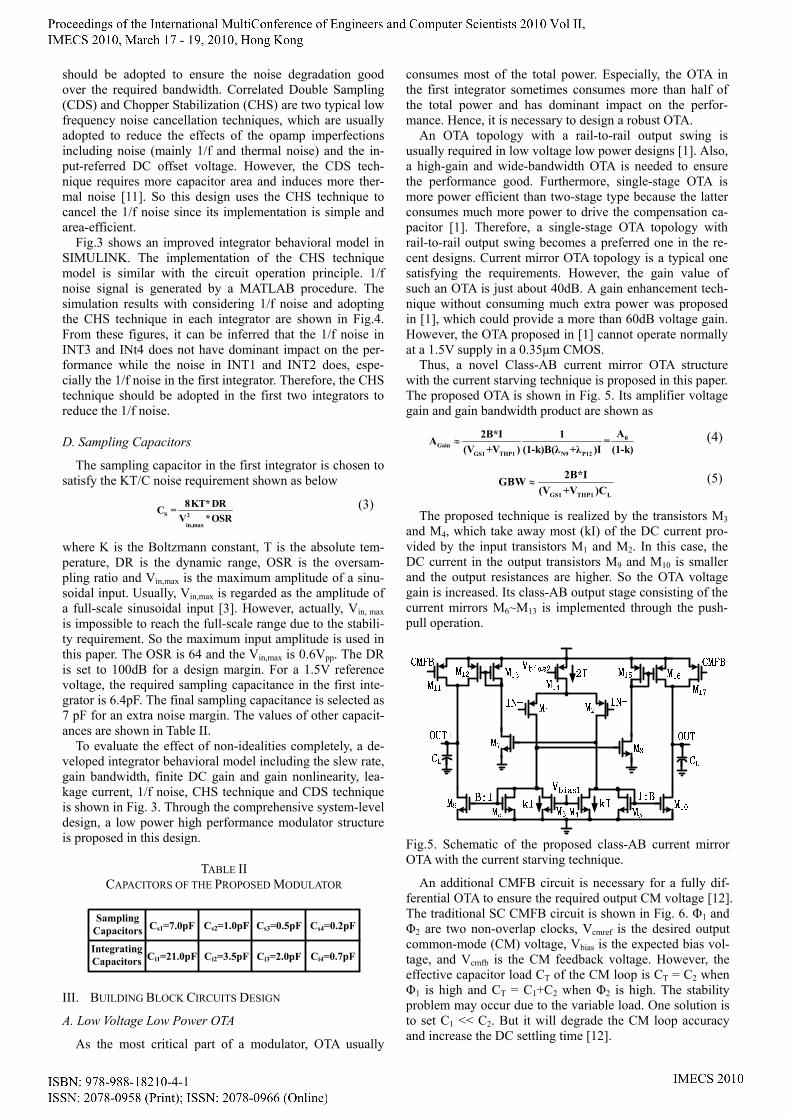
Thus, a novel Class-AB current mirror OTA structure with the current starving technique is proposed in this paper. The proposed OTA is shown in Fig. 5. Its amplifier voltage gain and gain bandwidth product are shown as
0Gain
GS1 THP1 N9 P12
A2B*I 1A =
(V +V ) (1-k)B(λ +λ )I (1-k) (4)
GS1 THP1 L
2B*IGBW
(V +V )C (5)
The proposed technique is realized by the transistors M3 and M4, which take away most (kI) of the DC current pro-vided by the input transistors M1 and M2. In this case, the DC current in the output transistors M9 and M10 is smaller and the output resistances are higher. So the OTA voltage gain is increased. Its class-AB output stage consisting of the current mirrors M6~M13 is implemented through the push- pull operation.
Fig.5. Schematic of the proposed class-AB current mirror OTA with the current starving technique.
An additional CMFB circuit is necessary for a fully dif-ferential OTA to ensure the required output CM voltage [12]. The traditional SC CMFB circuit is shown in Fig. 6. Φ1 and Φ2 are two non-overlap clocks, Vcmref is the desired output common-mode (CM) voltage, Vbias is the expected bias vol-tage, and Vcmfb is the CM feedback voltage. However, the effective capacitor load CT of the CM loop is CT = C2 when Φ1 is high and CT = C1+C2 when Φ2 is high. The stability problem may occur due to the variable load. One solution is to set C1 << C2. But it will degrade the CM loop accuracy and increase the DC settling time [12].
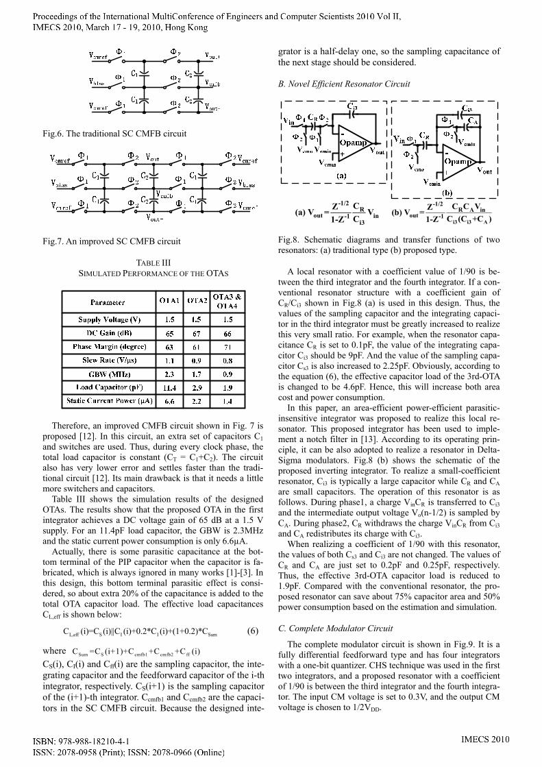
Fig.6. The traditional SC CMFB circuit
Fig.7. An improved SC CMFB circuit
TABLE III SIMULATED PERFORMANCE OF THE OTAS
Therefore, an improved CMFB circuit shown in Fig. 7 is proposed [12]. In this circuit, an extra set of capacitors C1 and switches are used. Thus, during every clock phase, the total load capacitor is constant (CT = C1+C2). The circuit also has very lower error and settles faster than the tradi-tional circuit [12]. Its main drawback is that it needs a little more switchers and capacitors.
Table III shows the simulation results of the designed OTAs. The results show that the proposed OTA in the first integrator achieves a DC voltage gain of 65 dB at a 1.5 V supply. For an 11.4pF load capacitor, the GBW is 2.3MHz and the static current power consumption is only 6.6µA.
Actually, there is some parasitic capacitance at the bot-tom terminal of the PIP capacitor when the capacitor is fa-bricated, which is always ignored in many works [1]-[3]. In this design, this bottom terminal parasitic effect is consi-dered, so about extra 20% of the capacitance is added to the total OTA capacitor load. The effective load capacitances CL,eff is shown below:
L,eff S I I SumC (i)=C (i)||C (i)+0.2*C (i)+(1+0.2)*C (6)
where Sum S cmfb1 cmfb2 ffC =C (i+1)+C +C +C (i)
CS(i), CI(i) and Cff(i) are the sampling capacitor, the inte-grating capacitor and the feedforward capacitor of the i-th integrator, respectively. CS(i+1) is the sampling capacitor of the (i+1)-th integrator. Ccmfb1 and Ccmfb2 are the capaci-tors in the SC CMFB circuit. Because the designed inte-
grator is a half-delay one, so the sampling capacitance of the next stage should be considered.
B. Novel Efficient Resonator Circuit
i3 i3 A
-1/2R A in
out -1
C C VZ(b) V =
C (C +C )1-Z
-1/2R
out in-1i3
CZ(a) V = V
C1-Z
Fig.8. Schematic diagrams and transfer functions of two resonators: (a) traditional type (b) proposed type.
A local resonator with a coefficient value of 1/90 is be-tween the third integrator and the fourth integrator. If a con-ventional resonator structure with a coefficient gain of CR/Ci3 shown in Fig.8 (a) is used in this design. Thus, the values of the sampling capacitor and the integrating capaci-tor in the third integrator must be greatly increased to realize this very small ratio. For example, when the resonator capa-citance CR is set to 0.1pF, the value of the integrating capa-citor Ci3 should be 9pF. And the value of the sampling capa-citor Cs3 is also increased to 2.25pF. Obviously, according to the equation (6), the effective capacitor load of the 3rd-OTA is changed to be 4.6pF. Hence, this will increase both area cost and power consumption.
In this paper, an area-efficient power-efficient parasitic- insensitive integrator was proposed to realize this local re-sonator. This proposed integrator has been used to imple-ment a notch filter in [13]. According to its operating prin-ciple, it can be also adopted to realize a resonator in Delta- Sigma modulators. Fig.8 (b) shows the schematic of the proposed inverting integrator. To realize a small-coefficient resonator, Ci3 is typically a large capacitor while CR and CA are small capacitors. The operation of this resonator is as follows. During phase1, a charge VinCR is transferred to Ci3 and the intermediate output voltage Vo(n-1/2) is sampled by CA. During phase2, CR withdraws the charge VinCR from Ci3 and CA redistributes its charge with Ci3.
When realizing a coefficient of 1/90 with this resonator, the values of both Cs3 and Ci3 are not changed. The values of CR and CA are just set to 0.2pF and 0.25pF, respectively. Thus, the effective 3rd-OTA capacitor load is reduced to 1.9pF. Compared with the conventional resonator, the pro-posed resonator can save about 75% capacitor area and 50% power consumption based on the estimation and simulation.
C. Complete Modulator Circuit
The complete modulator circuit is shown in Fig.9. It is a fully differential feedforward type and has four integrators with a one-bit quantizer. CHS technique was used in the first two integrators, and a proposed resonator with a coefficient of 1/90 is between the third integrator and the fourth integra-tor. The input CM voltage is set to 0.3V, and the output CM voltage is chosen to 1/2VDD.
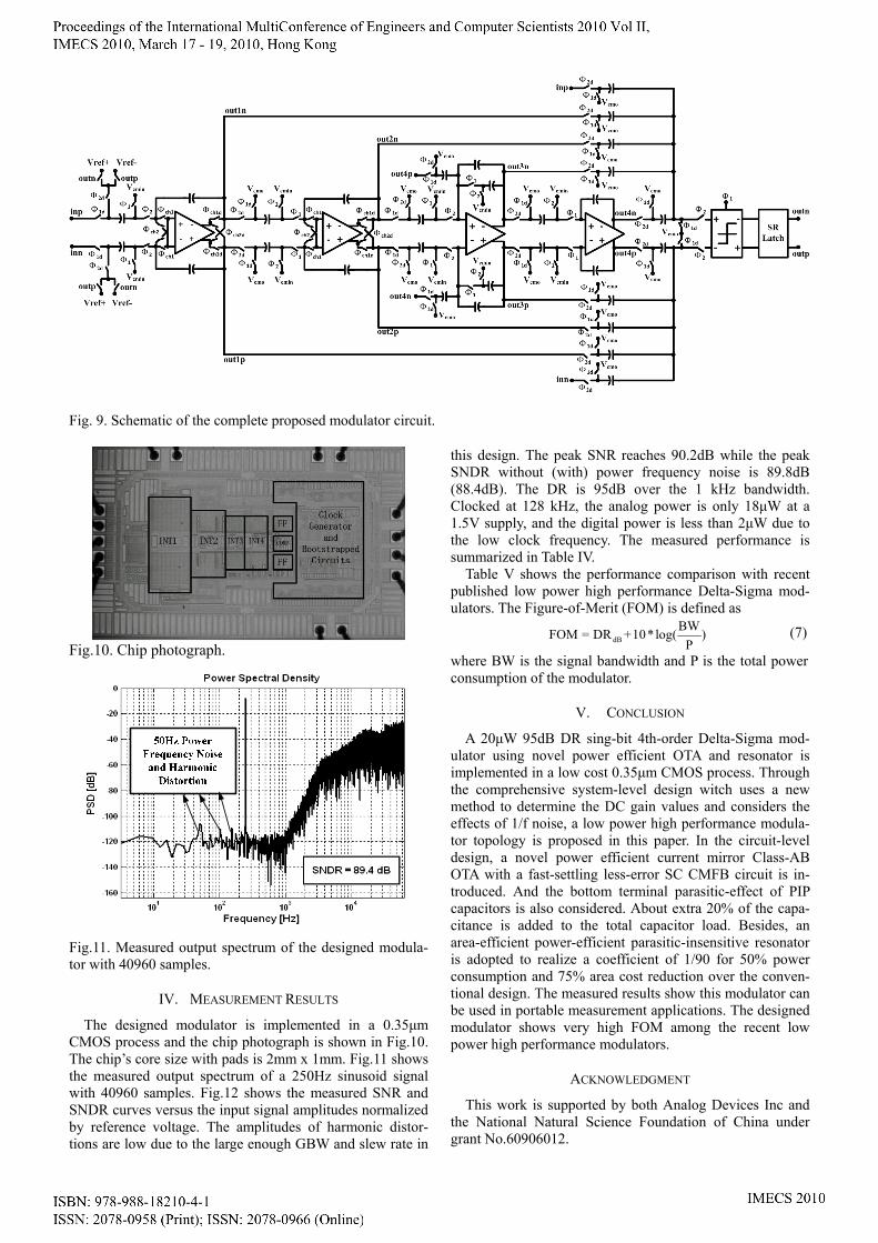
Fig. 9. Schematic of the complete proposed modulator circuit.
Fig.10. Chip photograph.
Fig.11. Measured output spectrum of the designed modula-tor with 40960 samples.
IV. MEASUREMENT RESULTS
The designed modulator is implemented in a 0.35μm CMOS process and the chip photograph is shown in Fig.10. The chip’s core size with pads is 2mm х 1mm. Fig.11 shows the measured output spectrum of a 250Hz sinusoid signal with 40960 samples. Fig.12 shows the measured SNR and SNDR curves versus the input signal amplitudes normalized by reference voltage. The amplitudes of harmonic distor-tions are low due to the large enough GBW and slew rate in
this design. The peak SNR reaches 90.2dB while the peak SNDR without (with) power frequency noise is 89.8dB (88.4dB). The DR is 95dB over the 1 kHz bandwidth. Clocked at 128 kHz, the analog power is only 18μW at a 1.5V supply, and the digital power is less than 2μW due to the low clock frequency. The measured performance is summarized in Table IV.
Table V shows the performance comparison with recent published low power high performance Delta-Sigma mod-ulators. The Figure-of-Merit (FOM) is defined as
dB
BWFOM = DR +10*log( )
P (7)
where BW is the signal bandwidth and P is the total power consumption of the modulator.
V. CONCLUSION
A 20μW 95dB DR sing-bit 4th-order Delta-Sigma mod-ulator using novel power efficient OTA and resonator is implemented in a low cost 0.35μm CMOS process. Through the comprehensive system-level design witch uses a new method to determine the DC gain values and considers the effects of 1/f noise, a low power high performance modula-tor topology is proposed in this paper. In the circuit-level design, a novel power efficient current mirror Class-AB OTA with a fast-settling less-error SC CMFB circuit is in-troduced. And the bottom terminal parasitic-effect of PIP capacitors is also considered. About extra 20% of the capa-citance is added to the total capacitor load. Besides, an area-efficient power-efficient parasitic-insensitive resonator is adopted to realize a coefficient of 1/90 for 50% power consumption and 75% area cost reduction over the conven-tional design. The measured results show this modulator can be used in portable measurement applications. The designed modulator shows very high FOM among the recent low power high performance modulators.
ACKNOWLEDGMENT
This work is supported by both Analog Devices Inc and the National Natural Science Foundation of China under grant No.60906012.
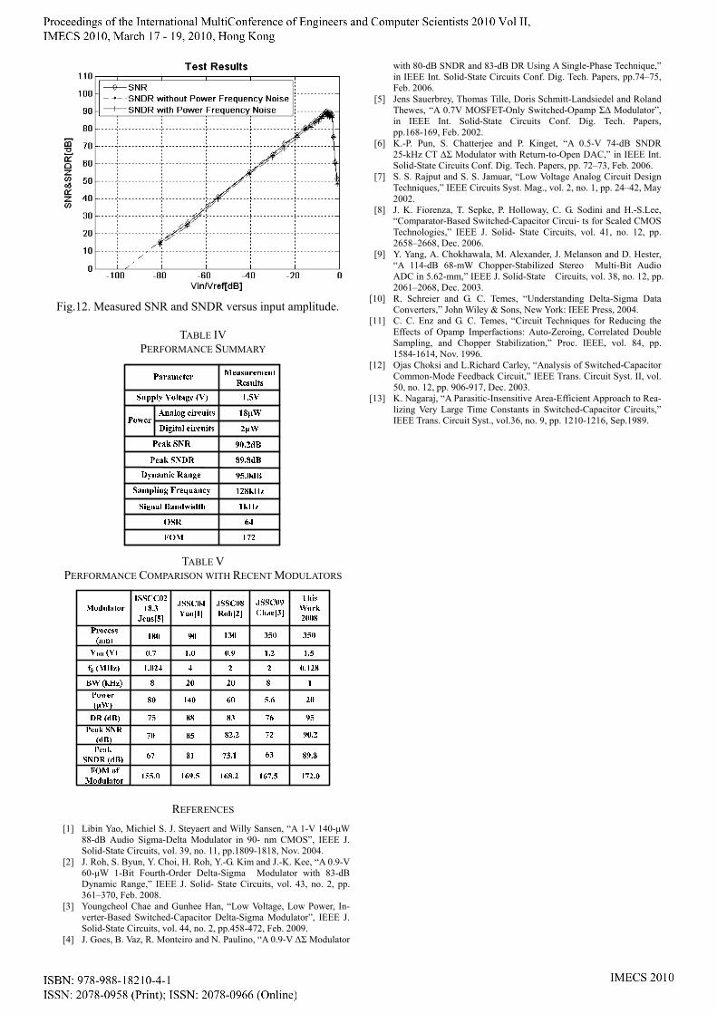
Fig.12. Measured SNR and SNDR versus input amplitude.
TABLE IV PERFORMANCE SUMMARY
TABLE V PERFORMANCE COMPARISON WITH RECENT MODULATORS
REFERENCES
[1] Libin Yao, Michiel S. J. Steyaert and Willy Sansen, “A 1-V 140-μW 88-dB Audio Sigma-Delta Modulator in 90- nm CMOS”, IEEE J. Solid-State Circuits, vol. 39, no. 11, pp.1809-1818, Nov. 2004.
[2] J. Roh, S. Byun, Y. Choi, H. Roh, Y.-G. Kim and J.-K. Kee, “A 0.9-V 60-μW 1-Bit Fourth-Order Delta-Sigma Modulator with 83-dB Dynamic Range,” IEEE J. Solid- State Circuits, vol. 43, no. 2, pp. 361–370, Feb. 2008.
[3] Youngcheol Chae and Gunhee Han, “Low Voltage, Low Power, In-verter-Based Switched-Capacitor Delta-Sigma Modulator”, IEEE J. Solid-State Circuits, vol. 44, no. 2, pp.458-472, Feb. 2009.
[4] J. Goes, B. Vaz, R. Monteiro and N. Paulino, “A 0.9-V ΔΣ Modulator
with 80-dB SNDR and 83-dB DR Using A Single-Phase Technique,” in IEEE Int. Solid-State Circuits Conf. Dig. Tech. Papers, pp.74–75, Feb. 2006.
[5] Jens Sauerbrey, Thomas Tille, Doris Schmitt-Landsiedel and Roland Thewes, “A 0.7V MOSFET-Only Switched-Opamp ΣΔ Modulator”, in IEEE Int. Solid-State Circuits Conf. Dig. Tech. Papers, pp.168-169, Feb. 2002.
[6] K.-P. Pun, S. Chatterjee and P. Kinget, “A 0.5-V 74-dB SNDR 25-kHz CT ΔΣ Modulator with Return-to-Open DAC,” in IEEE Int. Solid-State Circuits Conf. Dig. Tech. Papers, pp. 72–73, Feb. 2006.
[7] S. S. Rajput and S. S. Jamuar, “Low Voltage Analog Circuit Design Techniques,” IEEE Circuits Syst. Mag., vol. 2, no. 1, pp. 24–42, May 2002.
[8] J. K. Fiorenza, T. Sepke, P. Holloway, C. G. Sodini and H.-S.Lee, “Comparator-Based Switched-Capacitor Circui- ts for Scaled CMOS Technologies,” IEEE J. Solid- State Circuits, vol. 41, no. 12, pp. 2658–2668, Dec. 2006.
[9] Y. Yang, A. Chokhawala, M. Alexander, J. Melanson and D. Hester, “A 114-dB 68-mW Chopper-Stabilized Stereo Multi-Bit Audio ADC in 5.62-mm,” IEEE J. Solid-State Circuits, vol. 38, no. 12, pp. 2061–2068, Dec. 2003.
[10] R. Schreier and G. C. Temes, “Understanding Delta-Sigma Data Converters,” John Wiley & Sons, New York: IEEE Press, 2004.
[11] C. C. Enz and G. C. Temes, “Circuit Techniques for Reducing the Effects of Opamp Imperfactions: Auto-Zeroing, Correlated Double Sampling, and Chopper Stabilization,” Proc. IEEE, vol. 84, pp. 1584-1614, Nov. 1996.
[12] Ojas Choksi and L.Richard Carley, “Analysis of Switched-Capacitor Common-Mode Feedback Circuit,” IEEE Trans. Circuit Syst. II, vol. 50, no. 12, pp. 906-917, Dec. 2003.
[13] K. Nagaraj, “A Parasitic-Insensitive Area-Efficient Approach to Rea-lizing Very Large Time Constants in Switched-Capacitor Circuits,” IEEE Trans. Circuit Syst., vol.36, no. 9, pp. 1210-1216, Sep.1989.