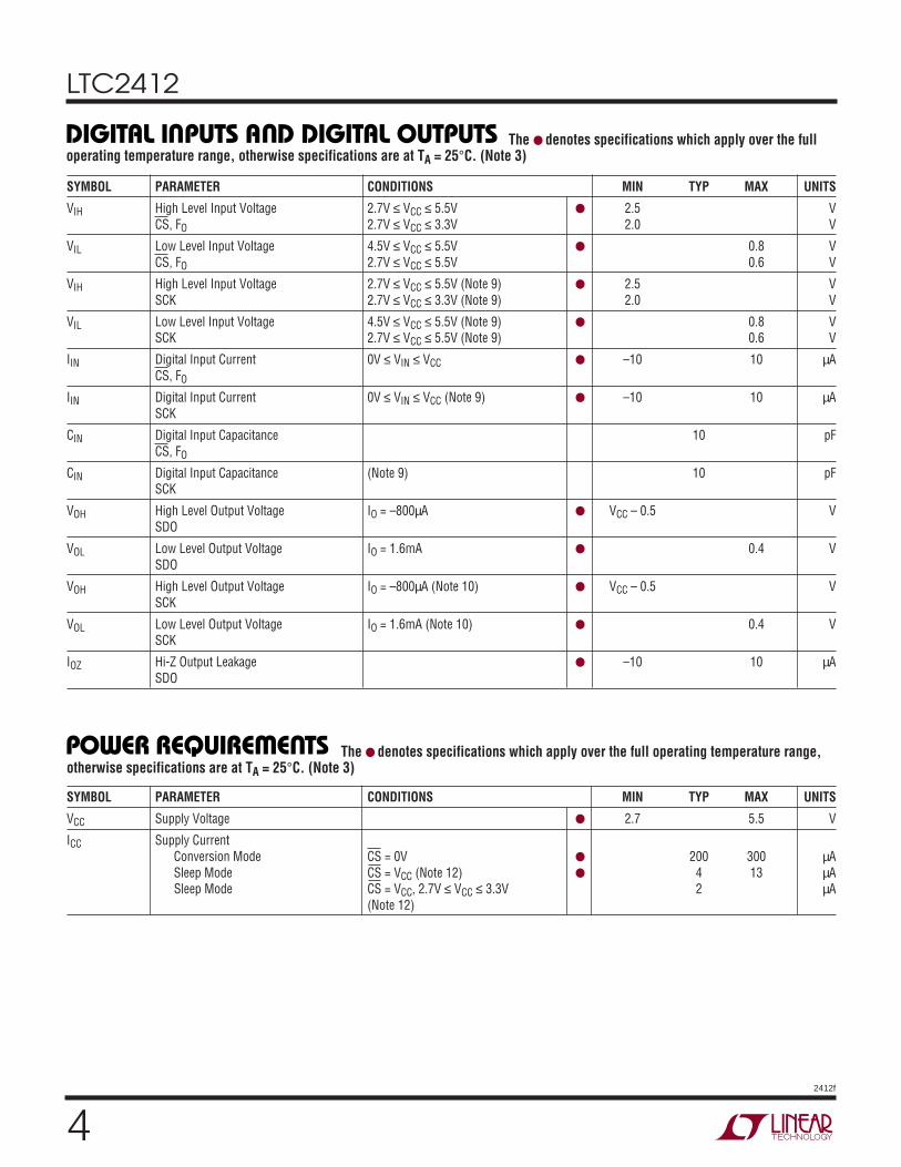
2412f - RS Components · 2019-10-12 · LTC2412 4 2412f SYMBOL PARAMETER CONDITIONS MIN TYP MAX...
36
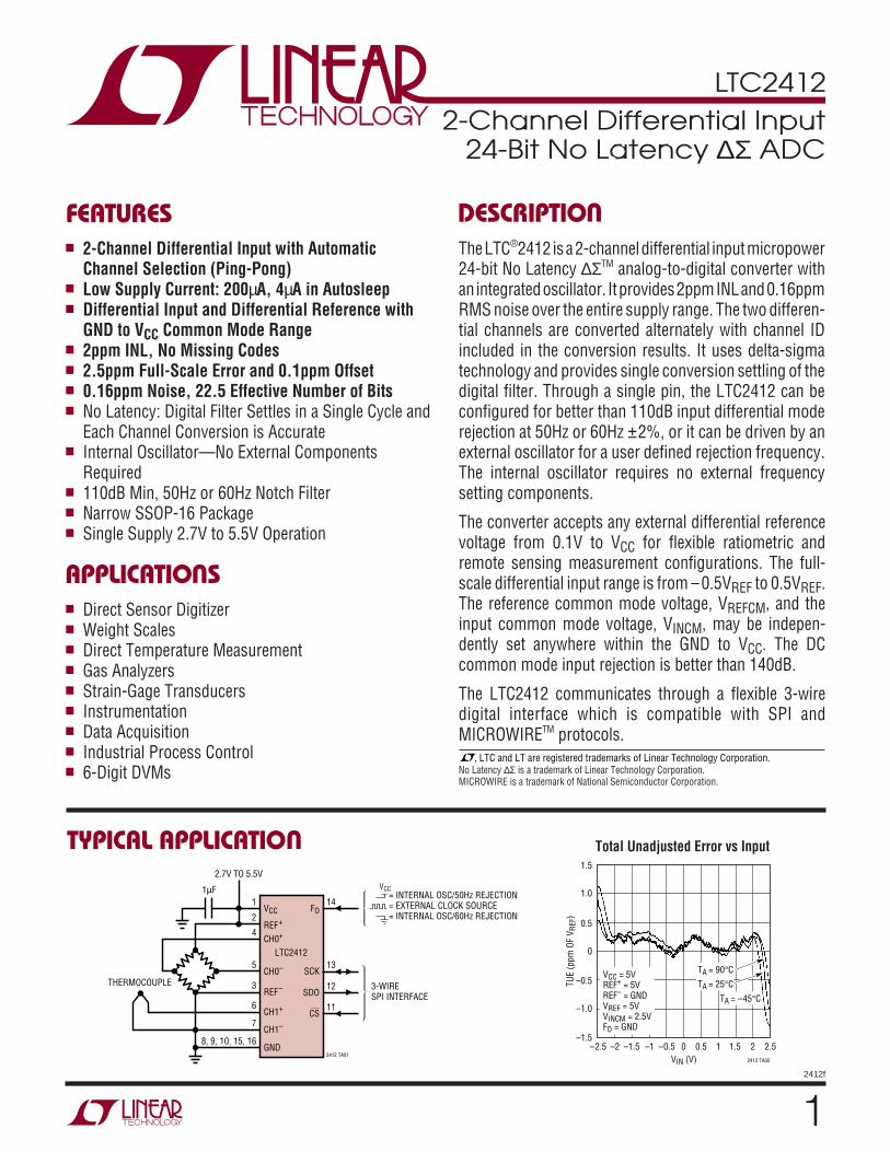
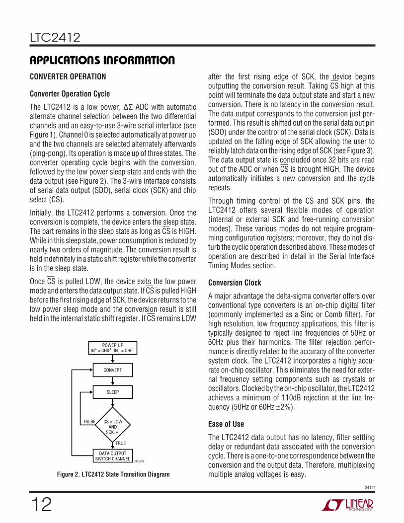
LTC2412 1 2412f The LTC ® 2412 is a 2-channel differential input micropower 24-bit No Latency ∆Σ TM analog-to-digital converter with an integrated oscillator. It provides 2ppm INL and 0.16ppm RMS noise over the entire supply range. The two differen- tial channels are converted alternately with channel ID included in the conversion results. It uses delta-sigma technology and provides single conversion settling of the digital filter. Through a single pin, the LTC2412 can be configured for better than 110dB input differential mode rejection at 50Hz or 60Hz ± 2%, or it can be driven by an external oscillator for a user defined rejection frequency. The internal oscillator requires no external frequency setting components. The converter accepts any external differential reference voltage from 0.1V to V CC for flexible ratiometric and remote sensing measurement configurations. The full- scale differential input range is from – 0.5V REF to 0.5V REF . The reference common mode voltage, V REFCM , and the input common mode voltage, V INCM , may be indepen- dently set anywhere within the GND to V CC . The DC common mode input rejection is better than 140dB. The LTC2412 communicates through a flexible 3-wire digital interface which is compatible with SPI and MICROWIRE TM protocols. ■ Direct Sensor Digitizer ■ Weight Scales ■ Direct Temperature Measurement ■ Gas Analyzers ■ Strain-Gage Transducers ■ Instrumentation ■ Data Acquisition ■ Industrial Process Control ■ 6-Digit DVMs , LTC and LT are registered trademarks of Linear Technology Corporation. ■ 2-Channel Differential Input with Automatic Channel Selection (Ping-Pong) ■ Low Supply Current: 200μ A, 4μ A in Autosleep ■ Differential Input and Differential Reference with GND to V CC Common Mode Range ■ 2ppm INL, No Missing Codes ■ 2.5ppm Full-Scale Error and 0.1ppm Offset ■ 0.16ppm Noise, 22.5 Effective Number of Bits ■ No Latency: Digital Filter Settles in a Single Cycle and Each Channel Conversion is Accurate ■ Internal Oscillator—No External Components Required ■ 110dB Min, 50Hz or 60Hz Notch Filter ■ Narrow SSOP-16 Package ■ Single Supply 2.7V to 5.5V Operation 2-Channel Differential Input 24-Bit No Latency ∆Σ ADC No Latency ∆Σ is a trademark of Linear Technology Corporation. MICROWIRE is a trademark of National Semiconductor Corporation. V CC REF + F O CH0 + CH0 – SCK REF – CH1 + SDO GND CS 1 14 4 13 3 5 THERMOCOUPLE 6 CH1 – 7 12 8, 9, 10, 15, 16 11 2412 TA01 2 = INTERNAL OSC/50Hz REJECTION = EXTERNAL CLOCK SOURCE = INTERNAL OSC/60Hz REJECTION 3-WIRE SPI INTERFACE 1μF 2.7V TO 5.5V LTC2412 V CC V IN (V) –1.5 TUE (ppm OF V REF ) –0.5 0.5 1.5 –1.0 0 1.0 –1.5 –0.5 0.5 1.5 2412 TA02 2.5 –2 –2.5 –1 0 1 2 T A = 90°C T A = –45°C T A = 25°C V CC = 5V REF + = 5V REF – = GND V REF = 5V V INCM = 2.5V F O = GND Total Unadjusted Error vs Input APPLICATIO S U FEATURES TYPICAL APPLICATIO U DESCRIPTIO U
Transcript of 2412f - RS Components · 2019-10-12 · LTC2412 4 2412f SYMBOL PARAMETER CONDITIONS MIN TYP MAX...
LTC2412
12412f
The LTC®2412 is a 2-channel differential input micropower24-bit No Latency ∆ΣTM analog-to-digital converter withan integrated oscillator. It provides 2ppm INL and 0.16ppmRMS noise over the entire supply range. The two differen-tial channels are converted alternately with channel IDincluded in the conversion results. It uses delta-sigmatechnology and provides single conversion settling of thedigital filter. Through a single pin, the LTC2412 can beconfigured for better than 110dB input differential moderejection at 50Hz or 60Hz ±2%, or it can be driven by anexternal oscillator for a user defined rejection frequency.The internal oscillator requires no external frequencysetting components.
The converter accepts any external differential referencevoltage from 0.1V to VCC for flexible ratiometric andremote sensing measurement configurations. The full-scale differential input range is from –0.5VREF to 0.5VREF.The reference common mode voltage, VREFCM, and theinput common mode voltage, VINCM, may be indepen-dently set anywhere within the GND to VCC. The DCcommon mode input rejection is better than 140dB.
The LTC2412 communicates through a flexible 3-wiredigital interface which is compatible with SPI andMICROWIRETM protocols.
Direct Sensor Digitizer Weight Scales Direct Temperature Measurement Gas Analyzers Strain-Gage Transducers Instrumentation Data Acquisition Industrial Process Control 6-Digit DVMs
, LTC and LT are registered trademarks of Linear Technology Corporation.
2-Channel Differential Input with AutomaticChannel Selection (Ping-Pong)
Low Supply Current: 200µA, 4µA in Autosleep Differential Input and Differential Reference with
GND to VCC Common Mode Range 2ppm INL, No Missing Codes 2.5ppm Full-Scale Error and 0.1ppm Offset 0.16ppm Noise, 22.5 Effective Number of Bits No Latency: Digital Filter Settles in a Single Cycle and
Each Channel Conversion is Accurate Internal Oscillator—No External Components
Required 110dB Min, 50Hz or 60Hz Notch Filter Narrow SSOP-16 Package Single Supply 2.7V to 5.5V Operation
2-Channel Differential Input24-Bit No Latency ∆Σ ADC
No Latency ∆Σ is a trademark of Linear Technology Corporation.MICROWIRE is a trademark of National Semiconductor Corporation.
VCC
REF+
FO
CH0+
CH0– SCK
REF–
CH1+
SDO
GND
CS
1 14
4
13
3
5
THERMOCOUPLE
6
CH1–7
12
8, 9, 10, 15, 16
11
2412 TA01
2
= INTERNAL OSC/50Hz REJECTION= EXTERNAL CLOCK SOURCE= INTERNAL OSC/60Hz REJECTION
3-WIRESPI INTERFACE
1µF
2.7V TO 5.5V
LTC2412
VCC
VIN (V)
–1.5
TUE
(ppm
OF
V REF
)
–0.5
0.5
1.5
–1.0
0
1.0
–1.5 –0.5 0.5 1.52412 TA02
2.5–2–2.5 –1 0 1 2
TA = 90°C
TA = –45°C
TA = 25°CVCC = 5VREF+ = 5VREF– = GNDVREF = 5VVINCM = 2.5VFO = GND
Total Unadjusted Error vs Input
APPLICATIO SU
FEATURES
TYPICAL APPLICATIO
U
DESCRIPTIO
U
LTC2412
22412f
ABSOLUTE AXI U RATI GS
W WW U
PACKAGE/ORDER I FOR ATIOU UW
ELECTRICAL CHARACTERISTICS
(Notes 1, 2)ORDER PART NUMBERSupply Voltage (VCC) to GND.......................–0.3V to 7V
Analog Input Voltage to GND .................................... –0.3V to (VCC + 0.3V)Reference Input Voltage to GND .................................... –0.3V to (VCC + 0.3V)Digital Input Voltage to GND ........ –0.3V to (VCC + 0.3V)Digital Output Voltage to GND ..... –0.3V to (VCC + 0.3V)Operating Temperature Range
LTC2412C ............................................... 0°C to 70°CLTC2412I ............................................ –40°C to 85°C
Storage Temperature Range ................. –65°C to 150°CLead Temperature (Soldering, 10 sec).................. 300°C
TJMAX = 125°C, θJA = 110°C/W
LTC2412CGNLTC2412IGN
PARAMETER CONDITIONS MIN TYP MAX UNITS
Resolution (No Missing Codes) 0.1V ≤ VREF ≤ VCC, –0.5 • VREF ≤ VIN ≤ 0.5 • VREF, (Note 5) 24 Bits
Integral Nonlinearity 5V ≤ VCC ≤ 5.5V, REF+ = 2.5V, REF– = GND, VINCM = 1.25V, (Note 6) 1 ppm of VREF5V ≤ VCC ≤ 5.5V, REF+ = 5V, REF– = GND, VINCM = 2.5V, (Note 6) 2 14 ppm of VREFREF+ = 2.5V, REF– = GND, VINCM = 1.25V, (Note 6) 5 ppm of VREF
Offset Error 2.5V ≤ REF+ ≤ VCC, REF– = GND, 0.5 2.5 µVGND ≤ IN+ = IN– ≤ VCC, (Note 14)
Offset Error Drift 2.5V ≤ REF+ ≤ VCC, REF– = GND, 10 nV/°CGND ≤ IN+ = IN– ≤ VCC
Positive Full-Scale Error 2.5V ≤ REF+ ≤ VCC, REF– = GND, 2.5 12 ppm of VREFIN+ = 0.75REF+, IN– = 0.25 • REF+
Positive Full-Scale Error Drift 2.5V ≤ REF+ ≤ VCC, REF– = GND, 0.03 ppm of VREF/°CIN+ = 0.75REF+, IN– = 0.25 • REF+
Negative Full-Scale Error 2.5V ≤ REF+ ≤ VCC, REF– = GND, 2.5 12 ppm of VREFIN+ = 0.25 • REF+, IN– = 0.75 • REF+
Negative Full-Scale Error Drift 2.5V ≤ REF+ ≤ VCC, REF– = GND, 0.03 ppm of VREF/°CIN+ = 0.25 • REF+, IN– = 0.75 • REF+
Total Unadjusted Error 5V ≤ VCC ≤ 5.5V, REF+ = 2.5V, REF– = GND, VINCM = 1.25V 3 ppm of VREF5V ≤ VCC ≤ 5.5V, REF+ = 5V, REF– = GND, VINCM = 2.5V 3 ppm of VREFREF+ = 2.5V, REF– = GND, VINCM = 1.25V, (Note 6) 4 ppm of VREF
Output Noise 5V ≤ VCC ≤ 5.5V, REF+ = 5V, REF – = GND, 0.8 µVRMSGND ≤ IN– = IN+ ≤ VCC, (Note 13)
The denotes specifications which apply over the full operatingtemperature range, otherwise specifications are at TA = 25°C. (Notes 3, 4)
GN PART MARKING
24122412I
TOP VIEW
GN PACKAGE16-LEAD PLASTIC SSOP
1
2
3
4
5
6
7
8
16
15
14
13
12
11
10
9
VCC
REF+
REF–
CH0+
CH0–
CH1+
CH1–
GND
GND
GND
FO
SCK
SDO
CS
GND
GND
Consult LTC Marketing for parts specified with wider operating temperature ranges.
LTC2412
32412f
SYMBOL PARAMETER CONDITIONS MIN TYP MAX UNITS
IN+ Absolute/Common Mode IN+ Voltage GND – 0.3 VCC + 0.3 V
IN– Absolute/Common Mode IN– Voltage GND – 0.3 VCC + 0.3 V
VIN Input Differential Voltage Range –VREF/2 VREF/2 V(IN+ – IN–)
REF+ Absolute/Common Mode REF+ Voltage 0.1 VCC V
REF– Absolute/Common Mode REF– Voltage GND VCC – 0.1 V
VREF Reference Differential Voltage Range 0.1 VCC V(REF+ – REF–)
CS (IN+) IN+ Sampling Capacitance 18 pF
CS (IN–) IN– Sampling Capacitance 18 pF
CS (REF+) REF+ Sampling Capacitance 18 pF
CS (REF–) REF– Sampling Capacitance 18 pF
IDC_LEAK (IN+) IN+ DC Leakage Current CS = VCC = 5.5V, IN+ = GND –10 1 10 nA
IDC_LEAK (IN–) IN– DC Leakage Current CS = VCC = 5.5V, IN– = 5.5V –10 1 10 nA
IDC_LEAK (REF+) REF+ DC Leakage Current CS = VCC = 5.5V, REF+ = 5.5V –10 1 10 nA
IDC_LEAK (REF–) REF– DC Leakage Current CS = VCC = 5.5V, REF– = GND –10 1 10 nA
The denotes specifications which apply over the full operatingtemperature range, otherwise specifications are at TA = 25°C. (Note 3)
The denotes specifications which apply over the full operatingtemperature range, otherwise specifications are at TA = 25°C. (Notes 3, 4)
PARAMETER CONDITIONS MIN TYP MAX UNITS
Input Common Mode Rejection DC 2.5V ≤ REF+ ≤ VCC, REF– = GND, 130 140 dBGND ≤ IN– = IN+ ≤ VCC (Note 5)
Input Common Mode Rejection 2.5V ≤ REF+ ≤ VCC, REF– = GND, 140 dB60Hz ±2% GND ≤ IN– = IN+ ≤ VCC, (Notes 5, 7)
Input Common Mode Rejection 2.5V ≤ REF+ ≤ VCC, REF– = GND, 140 dB50Hz ±2% GND ≤ IN– = IN+ ≤ VCC, (Notes 5, 8)
Input Normal Mode Rejection (Notes 5, 7) 110 140 dB60Hz ±2%
Input Normal Mode Rejection (Note 5, 8) 110 140 dB50Hz ±2%
Reference Common Mode 2.5V ≤ REF+ ≤ VCC, GND ≤ REF– ≤ 2.5V, 130 140 dBRejection DC VREF = 2.5V, IN– = IN+ = GND (Note 5)
Power Supply Rejection, DC REF+ = 2.5V, REF– = GND, IN– = IN+ = GND 120 dB
Power Supply Rejection, 60Hz ±2% REF+ = 2.5V, REF– = GND, IN– = IN+ = GND, (Note 7) 120 dB
Power Supply Rejection, 50Hz ±2% REF+ = 2.5V, REF– = GND, IN– = IN+ = GND, (Note 8) 120 dB
CO VERTER CHARACTERISTICS
U
A ALOG I PUT AU
D REFERE CEU UU
LTC2412
42412f
SYMBOL PARAMETER CONDITIONS MIN TYP MAX UNITS
VCC Supply Voltage 2.7 5.5 V
ICC Supply CurrentConversion Mode CS = 0V 200 300 µASleep Mode CS = VCC (Note 12) 4 13 µA
Sleep Mode CS = VCC, 2.7V ≤ VCC ≤ 3.3V 2 µA(Note 12)
The denotes specifications which apply over the full operating temperature range,otherwise specifications are at TA = 25°C. (Note 3)
The denotes specifications which apply over the fulloperating temperature range, otherwise specifications are at TA = 25°C. (Note 3)
SYMBOL PARAMETER CONDITIONS MIN TYP MAX UNITS
VIH High Level Input Voltage 2.7V ≤ VCC ≤ 5.5V 2.5 VCS, FO 2.7V ≤ VCC ≤ 3.3V 2.0 V
VIL Low Level Input Voltage 4.5V ≤ VCC ≤ 5.5V 0.8 VCS, FO 2.7V ≤ VCC ≤ 5.5V 0.6 V
VIH High Level Input Voltage 2.7V ≤ VCC ≤ 5.5V (Note 9) 2.5 VSCK 2.7V ≤ VCC ≤ 3.3V (Note 9) 2.0 V
VIL Low Level Input Voltage 4.5V ≤ VCC ≤ 5.5V (Note 9) 0.8 VSCK 2.7V ≤ VCC ≤ 5.5V (Note 9) 0.6 V
IIN Digital Input Current 0V ≤ VIN ≤ VCC –10 10 µACS, FO
IIN Digital Input Current 0V ≤ VIN ≤ VCC (Note 9) –10 10 µASCK
CIN Digital Input Capacitance 10 pFCS, FO
CIN Digital Input Capacitance (Note 9) 10 pFSCK
VOH High Level Output Voltage IO = –800µA VCC – 0.5 VSDO
VOL Low Level Output Voltage IO = 1.6mA 0.4 VSDO
VOH High Level Output Voltage IO = –800µA (Note 10) VCC – 0.5 VSCK
VOL Low Level Output Voltage IO = 1.6mA (Note 10) 0.4 VSCK
IOZ Hi-Z Output Leakage –10 10 µASDO
DIGITAL I PUTS A D DIGITAL OUTPUTS
UU
POWER REQUIRE E TS
W U
LTC2412
52412f
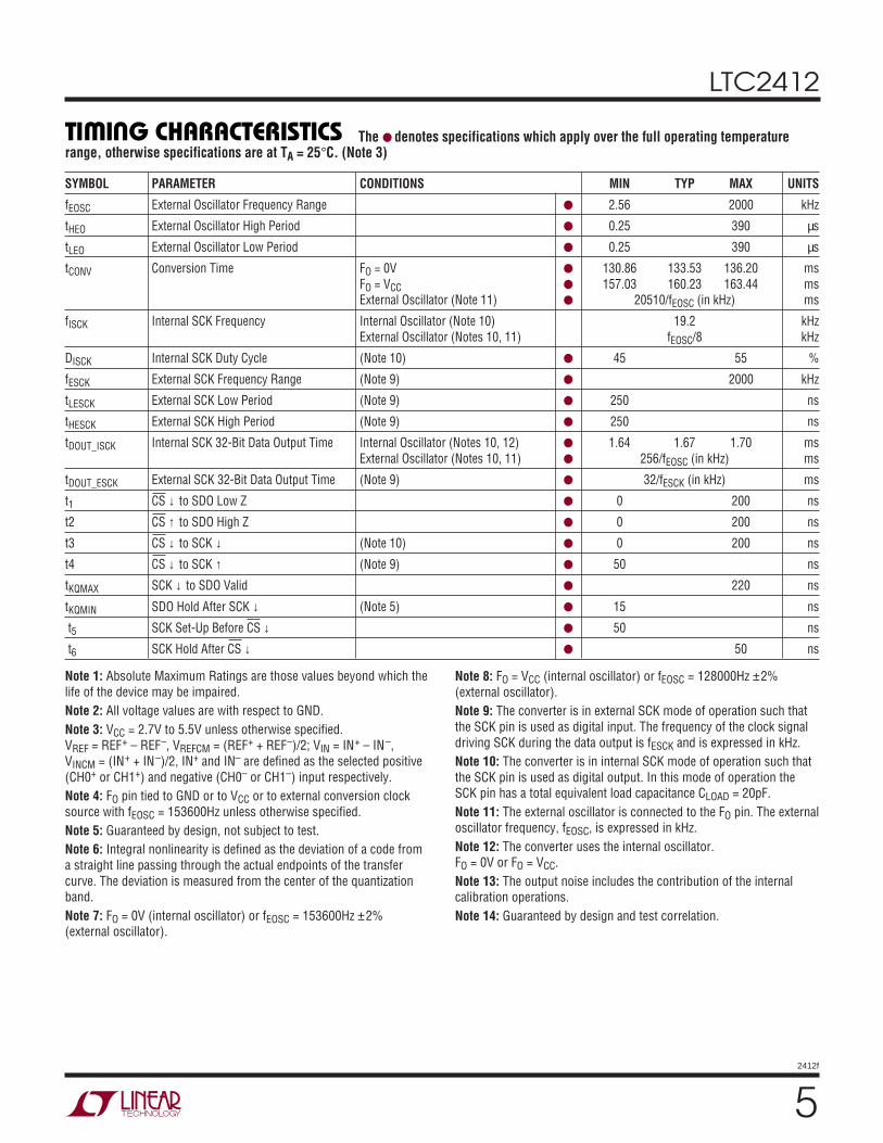
Note 1: Absolute Maximum Ratings are those values beyond which thelife of the device may be impaired.Note 2: All voltage values are with respect to GND.Note 3: VCC = 2.7V to 5.5V unless otherwise specified.VREF = REF+ – REF–, VREFCM = (REF+ + REF–)/2; VIN = IN+ – IN–,VINCM = (IN+ + IN–)/2, IN+ and IN– are defined as the selected positive(CH0+ or CH1+) and negative (CH0– or CH1–) input respectively.Note 4: FO pin tied to GND or to VCC or to external conversion clocksource with fEOSC = 153600Hz unless otherwise specified.Note 5: Guaranteed by design, not subject to test.Note 6: Integral nonlinearity is defined as the deviation of a code froma straight line passing through the actual endpoints of the transfercurve. The deviation is measured from the center of the quantizationband.Note 7: FO = 0V (internal oscillator) or fEOSC = 153600Hz ±2%(external oscillator).
Note 8: FO = VCC (internal oscillator) or fEOSC = 128000Hz ±2%(external oscillator).Note 9: The converter is in external SCK mode of operation such thatthe SCK pin is used as digital input. The frequency of the clock signaldriving SCK during the data output is fESCK and is expressed in kHz.Note 10: The converter is in internal SCK mode of operation such thatthe SCK pin is used as digital output. In this mode of operation theSCK pin has a total equivalent load capacitance CLOAD = 20pF.Note 11: The external oscillator is connected to the FO pin. The externaloscillator frequency, fEOSC, is expressed in kHz.Note 12: The converter uses the internal oscillator.FO = 0V or FO = VCC.Note 13: The output noise includes the contribution of the internalcalibration operations.Note 14: Guaranteed by design and test correlation.
SYMBOL PARAMETER CONDITIONS MIN TYP MAX UNITS
fEOSC External Oscillator Frequency Range 2.56 2000 kHz
tHEO External Oscillator High Period 0.25 390 µs
tLEO External Oscillator Low Period 0.25 390 µs
tCONV Conversion Time FO = 0V 130.86 133.53 136.20 msFO = VCC 157.03 160.23 163.44 msExternal Oscillator (Note 11) 20510/fEOSC (in kHz) ms
fISCK Internal SCK Frequency Internal Oscillator (Note 10) 19.2 kHzExternal Oscillator (Notes 10, 11) fEOSC/8 kHz
DISCK Internal SCK Duty Cycle (Note 10) 45 55 %
fESCK External SCK Frequency Range (Note 9) 2000 kHz
tLESCK External SCK Low Period (Note 9) 250 ns
tHESCK External SCK High Period (Note 9) 250 ns
tDOUT_ISCK Internal SCK 32-Bit Data Output Time Internal Oscillator (Notes 10, 12) 1.64 1.67 1.70 msExternal Oscillator (Notes 10, 11) 256/fEOSC (in kHz) ms
tDOUT_ESCK External SCK 32-Bit Data Output Time (Note 9) 32/fESCK (in kHz) ms
t1 CS ↓ to SDO Low Z 0 200 ns
t2 CS ↑ to SDO High Z 0 200 ns
t3 CS ↓ to SCK ↓ (Note 10) 0 200 ns
t4 CS ↓ to SCK ↑ (Note 9) 50 ns
tKQMAX SCK ↓ to SDO Valid 220 ns
tKQMIN SDO Hold After SCK ↓ (Note 5) 15 ns
t5 SCK Set-Up Before CS ↓ 50 ns
t6 SCK Hold After CS ↓ 50 ns
The denotes specifications which apply over the full operating temperaturerange, otherwise specifications are at TA = 25°C. (Note 3)TI I G CHARACTERISTICS
WU
LTC2412
62412f
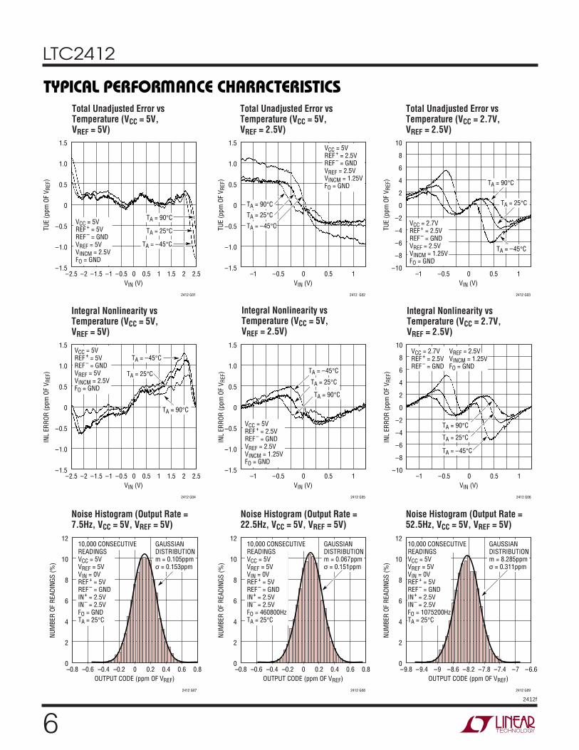
TYPICAL PERFOR A CE CHARACTERISTICS
UW
Total Unadjusted Error vsTemperature (VCC = 2.7V,VREF = 2.5V)
Total Unadjusted Error vsTemperature (VCC = 5V,VREF = 2.5V)
Total Unadjusted Error vsTemperature (VCC = 5V,VREF = 5V)
Integral Nonlinearity vsTemperature (VCC = 2.7V,VREF = 2.5V)
Integral Nonlinearity vsTemperature (VCC = 5V,VREF = 2.5V)
Integral Nonlinearity vsTemperature (VCC = 5V,VREF = 5V)
Noise Histogram (Output Rate =52.5Hz, VCC = 5V, VREF = 5V)
Noise Histogram (Output Rate =22.5Hz, VCC = 5V, VREF = 5V)
Noise Histogram (Output Rate =7.5Hz, VCC = 5V, VREF = 5V)
VIN (V)–2.5 –2 –1.5 –1 –0.5 0 0.5 1 1.5 2 2.5
TUE
(ppm
OF
V REF
)
2412 G01
1.5
1.0
0.5
0
–0.5
–1.0
–1.5
VCC = 5VREF + = 5VREF – = GNDVREF = 5VVINCM = 2.5VFO = GND
TA = 90°C
TA = 25°C
TA = –45°C
VIN (V)–1 –0.5 0 0.5 1
TUE
(ppm
OF
V REF
)
2412 G02
1.5
1.0
0.5
0
–0.5
–1.0
–1.5
VCC = 5VREF + = 2.5VREF – = GNDVREF = 2.5VVINCM = 1.25VFO = GND
TA = 90°C
TA = 25°C
TA = –45°C
VIN (V)–1 –0.5 0 0.5 1
TUE
(ppm
OF
V REF
)
2412 G03
10
8
6
4
2
0
–2
–4
–6
–8
–10
VCC = 2.7VREF + = 2.5VREF – = GNDVREF = 2.5VVINCM = 1.25VFO = GND
TA = 90°C
TA = 25°C
TA = –45°C
VIN (V)–2.5 –2 –1.5 –1 –0.5 0 0.5 1 1.5 2 2.5
INL
ERRO
R (p
pm O
F V R
EF)
2412 G04
1.5
1.0
0.5
0
–0.5
–1.0
–1.5
VCC = 5VREF + = 5VREF – = GNDVREF = 5VVINCM = 2.5VFO = GND
TA = –45°C
TA = 25°C
TA = 90°C
VIN (V)–1 –0.5 0 0.5 1
INL
ERRO
R (p
pm O
F V R
EF)
2412 G05
1.5
1.0
0.5
0
–0.5
–1.0
–1.5
VCC = 5VREF + = 2.5VREF – = GNDVREF = 2.5VVINCM = 1.25VFO = GND
TA = 25°C
TA = –45°C
TA = 90°C
VIN (V)–1 –0.5 0 0.5 1
INL
ERRO
R (p
pm O
F V R
EF)
2412 G06
10
8
6
4
2
0
–2
–4
–6
–8
–10
VREF = 2.5VVINCM = 1.25VFO = GND
VCC = 2.7VREF + = 2.5VREF – = GND
TA = 25°C
TA = –45°C
TA = 90°C
OUTPUT CODE (ppm OF VREF)–0.8 –0.6 –0.4 –0.2 0 0.2 0.4 0.6 0.8
NUM
BER
OF R
EADI
NGS
(%)
2412 G07
12
10
8
6
4
2
0
10,000 CONSECUTIVEREADINGSVCC = 5VVREF = 5VVIN = 0VREF + = 5VREF – = GNDIN+ = 2.5VIN– = 2.5VFO = GNDTA = 25°C
GAUSSIANDISTRIBUTIONm = 0.105ppmσ = 0.153ppm
OUTPUT CODE (ppm OF VREF)–0.8 –0.6 –0.4 –0.2 0 0.2 0.4 0.6 0.8
NUM
BER
OF R
EADI
NGS
(%)
2412 G08
12
10
8
6
4
2
0
10,000 CONSECUTIVEREADINGSVCC = 5VVREF = 5VVIN = 0VREF + = 5VREF – = GNDIN+ = 2.5VIN– = 2.5VFO = 460800HzTA = 25°C
GAUSSIANDISTRIBUTIONm = 0.067ppmσ = 0.151ppm
OUTPUT CODE (ppm OF VREF)–9.8 –9.4 –9 –8.6 –8.2 –7.8 –7.4 –7 –6.6
NUM
BER
OF R
EADI
NGS
(%)
2412 G09
12
10
8
6
4
2
0
10,000 CONSECUTIVEREADINGSVCC = 5VVREF = 5VVIN = 0VREF + = 5VREF – = GNDIN+ = 2.5VIN– = 2.5VFO = 1075200HzTA = 25°C
GAUSSIANDISTRIBUTIONm = 8.285ppmσ = 0.311ppm
LTC2412
72412f
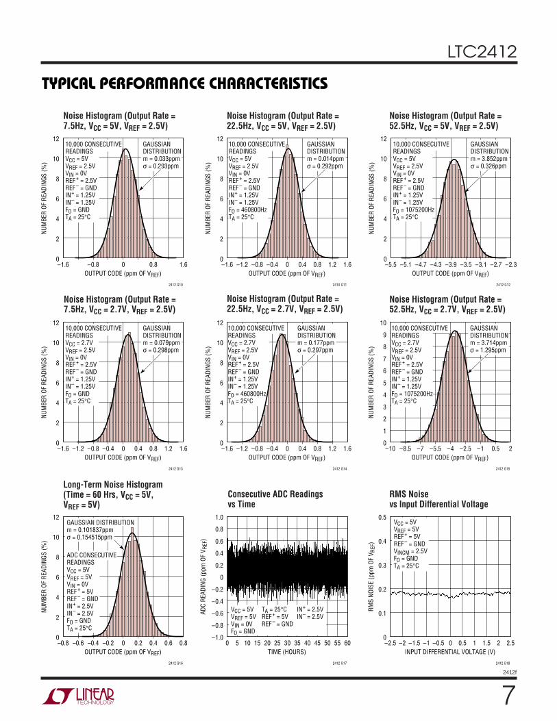
TYPICAL PERFOR A CE CHARACTERISTICS
UW
OUTPUT CODE (ppm OF VREF)–1.6 –0.8 0 0.8 1.6
NUM
BER
OF R
EADI
NGS
(%)
2412 G10
12
10
8
6
4
2
0
10,000 CONSECUTIVEREADINGSVCC = 5VVREF = 2.5VVIN = 0VREF + = 2.5VREF – = GNDIN+ = 1.25VIN– = 1.25VFO = GNDTA = 25°C
GAUSSIANDISTRIBUTIONm = 0.033ppmσ = 0.293ppm
OUTPUT CODE (ppm OF VREF)–1.6 –1.2 –0.8 –0.4 0 0.4 0.8 1.2 1.6
NUM
BER
OF R
EADI
NGS
(%)
2410 G11
12
10
8
6
4
2
0
10,000 CONSECUTIVEREADINGSVCC = 5VVREF = 2.5VVIN = 0VREF + = 2.5VREF – = GNDIN+ = 1.25VIN– = 1.25VFO = 460800HzTA = 25°C
GAUSSIANDISTRIBUTIONm = 0.014ppmσ = 0.292ppm
OUTPUT CODE (ppm OF VREF)–5.5 –5.1 –4.7 –4.3 –3.9 –3.5 –3.1 –2.7 –2.3
NUM
BER
OF R
EADI
NGS
(%)
2412 G12
12
10
8
6
4
2
0
10,000 CONSECUTIVEREADINGSVCC = 5VVREF = 2.5VVIN = 0VREF + = 2.5VREF – = GNDIN+ = 1.25VIN– = 1.25VFO = 1075200HzTA = 25°C
GAUSSIANDISTRIBUTIONm = 3.852ppmσ = 0.326ppm
OUTPUT CODE (ppm OF VREF)–1.6 –1.2 –0.8 –0.4 0 0.4 0.8 1.2 1.6
NUM
BER
OF R
EADI
NGS
(%)
2412 G13
12
10
8
6
4
2
0
10,000 CONSECUTIVEREADINGSVCC = 2.7VVREF = 2.5VVIN = 0VREF + = 2.5VREF – = GNDIN+ = 1.25VIN– = 1.25VFO = GNDTA = 25°C
GAUSSIANDISTRIBUTIONm = 0.079ppmσ = 0.298ppm
OUTPUT CODE (ppm OF VREF)–1.6 –1.2 –0.8 –0.4 0 0.4 0.8 1.2 1.6
NUM
BER
OF R
EADI
NGS
(%)
2412 G14
12
10
8
6
4
2
0
10,000 CONSECUTIVEREADINGSVCC = 2.7VVREF = 2.5VVIN = 0VREF + = 2.5VREF – = GNDIN+ = 1.25VIN– = 1.25VFO = 460800HzTA = 25°C
GAUSSIANDISTRIBUTIONm = 0.177ppmσ = 0.297ppm
OUTPUT CODE (ppm OF VREF)–10 –8.5 –7 –5.5 –4 –2.5 –1 0.5 2
NUM
BER
OF R
EADI
NGS
(%)
2412 G15
10
9
8
7
6
5
4
3
2
1
0
10,000 CONSECUTIVEREADINGSVCC = 2.7VVREF = 2.5VVIN = 0VREF + = 2.5VREF – = GNDIN+ = 1.25VIN– = 1.25VFO = 1075200HzTA = 25°C
GAUSSIANDISTRIBUTIONm = 3.714ppmσ = 1.295ppm
OUTPUT CODE (ppm OF VREF)–0.8 –0.6 –0.4 –0.2 0 0.2 0.4 0.6 0.8
NUM
BER
OF R
EADI
NGS
(%)
2412 G16
12
10
8
6
4
2
0
ADC CONSECUTIVEREADINGSVCC = 5VVREF = 5VVIN = 0VREF + = 5VREF – = GNDIN+ = 2.5VIN– = 2.5VFO = GNDTA = 25°C
GAUSSIAN DISTRIBUTIONm = 0.101837ppmσ = 0.154515ppm
TIME (HOURS)0 5 10 15 20 25 30 35 40 45 50 55 60
ADC
READ
ING
(ppm
OF
V REF
)
2412 G17
1.0
0.8
0.6
0.4
0.2
0
–0.2
–0.4
–0.6
–0.8
–1.0
VCC = 5VVREF = 5VVIN = 0VFO = GND
TA = 25°CREF + = 5VREF – = GND
IN+ = 2.5VIN– = 2.5V
INPUT DIFFERENTIAL VOLTAGE (V)–2.5 –2 –1.5 –1 –0.5 0 0.5 1 1.5 2 2.5
RMS
NOIS
E (p
pm O
F V R
EF)
2412 G18
0.5
0.4
0.3
0.2
0.1
0
VCC = 5VVREF = 5VREF + = 5VREF – = GNDVINCM = 2.5VFO = GNDTA = 25°C
Noise Histogram (Output Rate =52.5Hz, VCC = 5V, VREF = 2.5V)
Noise Histogram (Output Rate =22.5Hz, VCC = 5V, VREF = 2.5V)
Noise Histogram (Output Rate =7.5Hz, VCC = 5V, VREF = 2.5V)
Noise Histogram (Output Rate =52.5Hz, VCC = 2.7V, VREF = 2.5V)
Noise Histogram (Output Rate =22.5Hz, VCC = 2.7V, VREF = 2.5V)
Noise Histogram (Output Rate =7.5Hz, VCC = 2.7V, VREF = 2.5V)
RMS Noisevs Input Differential Voltage
Consecutive ADC Readingsvs Time
Long-Term Noise Histogram(Time = 60 Hrs, VCC = 5V,VREF = 5V)
LTC2412
82412f
TYPICAL PERFOR A CE CHARACTERISTICS
UW
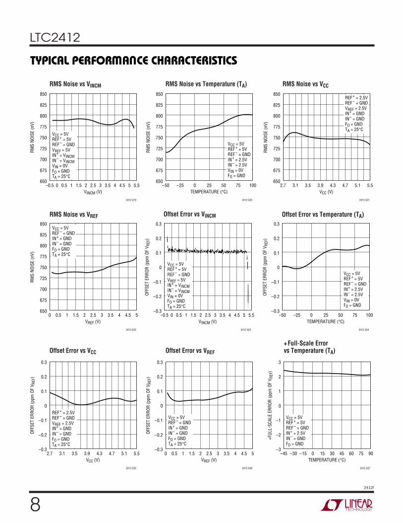
RMS Noise vs VCCRMS Noise vs Temperature (TA)RMS Noise vs VINCM
Offset Error vs Temperature (TA)Offset Error vs VINCMRMS Noise vs VREF
+Full-Scale Errorvs Temperature (TA)Offset Error vs VREFOffset Error vs VCC
VINCM (V)–0.5 0 10.5 1.5 2 2.5 3 3.5 4 4.5 5 5.5
RMS
NOIS
E (n
V)
2412 G19
850
825
800
775
750
725
700
675
650
VCC = 5VREF + = 5VREF – = GNDVREF = 5VIN+ = VINCMIN– = VINCMVIN = 0VFO = GNDTA = 25°C
TEMPERATURE (°C)
RMS
NOIS
E (n
V)
2412 G20
850
825
800
775
750
725
700
675
650–50 –25 0 25 50 75 100
VCC = 5VREF + = 5VREF – = GNDIN+ = 2.5VIN– = 2.5VVIN = 0VFO = GND
VCC (V)2.7 3.1 3.5 3.9 4.3 4.7 5.1 5.5
RMS
NOIS
E (n
V)
2412 G21
850
825
800
775
750
725
700
675
650
REF + = 2.5VREF – = GNDVREF = 2.5VIN+ = GNDIN– = GNDFO = GNDTA = 25°C
VREF (V)0 0.5 1 1.5 2 2.5 3 3.5 4 4.5 5
RMS
NOIS
E (n
V)
2412 G22
850
825
800
775
750
725
700
675
650
VCC = 5VREF – = GNDIN+ = GNDIN– = GNDFO = GNDTA = 25°C
VINCM (V)–0.5 0 10.5 1.5 2 2.5 3 3.5 4 4.5 5 5.5
OFFS
ET E
RROR
(ppm
OF
V REF
)
2412 G23
0.3
0.2
0.1
0
–0.1
–0.2
–0.3
VCC = 5VREF + = 5VREF – = GNDVREF = 5VIN+ = VINCMIN– = VINCMVIN = 0VFO = GNDTA = 25°C
TEMPERATURE (°C)–50 –25 0 25 50 75 100
OFFS
ET E
RROR
(ppm
OF
V REF
)
2412 G24
0.3
0.2
0.1
0
–0.1
–0.2
–0.3
VCC = 5VREF + = 5VREF – = GNDIN+ = 2.5VIN– = 2.5VVIN = 0VFO = GND
VCC (V)
OFFS
ET E
RROR
(ppm
OF
V REF
)
2412 G25
0.3
0.2
0.1
0
–0.1
–0.2
–0.3
REF + = 2.5VREF – = GNDVREF = 2.5VIN+ = GNDIN– = GNDFO = GNDTA = 25°C
2.7 3.1 3.5 3.9 4.3 4.7 5.1 5.5VREF (V)
OFFS
ET E
RROR
(ppm
OF
V REF
)
2412 G26
0.3
0.2
0.1
0
–0.1
–0.2
–0.3
VCC = 5VREF – = GNDIN+ = GNDIN– = GNDFO = GNDTA = 25°C
0 0.5 1 1.5 2 2.5 3 3.5 4 4.5 5TEMPERATURE (°C)
+FUL
L-SC
ALE
ERRO
R (p
pm O
F V R
EF)
2412 G27
3
2
1
0
–1
–2
–3–45 –30 –15 0 15 30 45 60 75 90
VCC = 5VREF + = 5VREF – = GNDIN+ = 2.5VIN– = GNDFO = GND
LTC2412
92412f
TYPICAL PERFOR A CE CHARACTERISTICS
UW
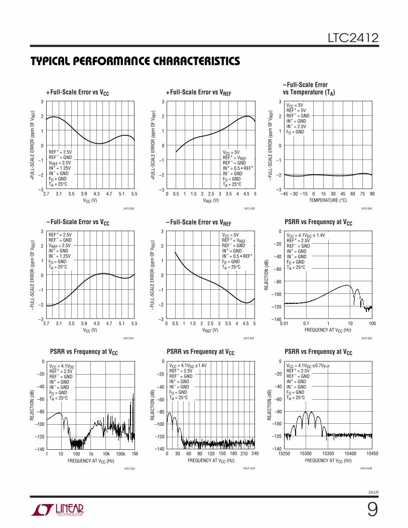
–Full-Scale Errorvs Temperature (TA)+Full-Scale Error vs VREF+Full-Scale Error vs VCC
PSRR vs Frequency at VCC–Full-Scale Error vs VREF–Full-Scale Error vs VCC
PSRR vs Frequency at VCCPSRR vs Frequency at VCCPSRR vs Frequency at VCC
VCC (V)
+FUL
L-SC
ALE
ERRO
R (p
pm O
F V R
EF)
2412 G28
3
2
1
0
–1
–2
–3
REF + = 2.5VREF – = GNDVREF = 2.5VIN+ = 1.25VIN– = GNDFO = GNDTA = 25°C
2.7 3.1 3.5 3.9 4.3 4.7 5.1 5.5VREF (V)
+FUL
L-SC
ALE
ERRO
R (p
pm O
F V R
EF)
2412 G29
3
2
1
0
–1
–2
–3
VCC = 5VREF + = VREFREF – = GNDIN+ = 0.5 • REF+
IN– = GNDFO = GNDTA = 25°C
0 0.5 1 1.5 2 2.5 3 3.5 4 4.5 5TEMPERATURE (°C)
–FUL
L-SC
ALE
ERRO
R (p
pm O
F V R
EF)
2412 G30
3
2
1
0
–1
–2
–3–45 –30 –15 0 15 30 45 60 75 90
VCC = 5VREF + = 5VREF – = GNDIN+ = GNDIN– = 2.5VFO = GND
VCC (V)
–FUL
L-SC
ALE
ERRO
R (p
pm O
F V R
EF)
2412 G31
3
2
1
0
–1
–2
–3
REF + = 2.5VREF – = GNDVREF = 2.5VIN+ = GNDIN– = 1.25VFO = GNDTA = 25°C
2.7 3.1 3.5 3.9 4.3 4.7 5.1 5.5VREF (V)
–FUL
L-SC
ALE
ERRO
R (p
pm O
F V R
EF)
2412 G32
3
2
1
0
–1
–2
–3
VCC = 5VREF + = VREFREF – = GNDIN+ = GNDIN– = 0.5 • REF+
FO = GNDTA = 25°C
0 0.5 1 1.5 2 2.5 3 3.5 4 4.5 5FREQUENCY AT VCC (Hz)
REJE
CTIO
N (d
B)
2412 G33
0
–20
–40
–60
–80
–100
–120
–1400.01 0.1 1 10 100
VCC = 4.1VDC ± 1.4VREF + = 2.5VREF – = GNDIN+ = GNDIN– = GNDFO = GNDTA = 25°C
FREQUENCY AT VCC (Hz)1
0
–20
–40
–60
–80
–100
–120
–1401k 100k
2412 G34
10 100 10k 1M
REJE
CTIO
N (d
B)
VCC = 4.1VDCREF + = 2.5VREF – = GNDIN+ = GNDIN– = GNDFO = GNDTA = 25°C
FREQUENCY AT VCC (Hz)0
REJE
CTIO
N (d
B)
–60
–40
–20
120 210
2412 G35
–80
–100
30 60 150 180
–120
–140
0
90 240
VCC = 4.1VDC ±1.4VREF + = 2.5VREF – = GNDIN+ = GNDIN– = GNDFO = GNDTA = 25°C
FREQUENCY AT VCC (Hz)15250
–60
–40
0
15400
2412 G36
–80
–100
15300 15350 15450
–120
–140
–20
REJE
CTIO
N (d
B)
VCC = 4.1VDC ±0.7VP-PREF + = 2.5VREF – = GNDIN+ = GNDIN– = GNDFO = GNDTA = 25°C
LTC2412
102412f
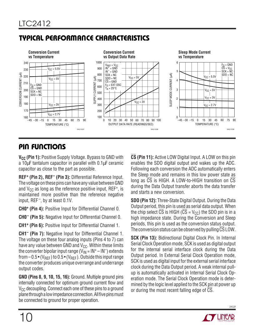
VCC (Pin 1): Positive Supply Voltage. Bypass to GND witha 10µF tantalum capacitor in parallel with 0.1µF ceramiccapacitor as close to the part as possible.
REF+ (Pin 2), REF– (Pin 3): Differential Reference Input.The voltage on these pins can have any value between GNDand VCC as long as the reference positive input, REF+, ismaintained more positive than the reference negativeinput, REF –, by at least 0.1V.
CH0+ (Pin 4): Positive Input for Differential Channel 0.
CH0– (Pin 5): Negative Input for Differential Channel 0.
CH1+ (Pin 6): Positive Input for Differential Channel 1.
CH1– (Pin 7): Negative Input for Differential Channel 1.The voltage on these four analog inputs (Pins 4 to 7) canhave any value between GND and VCC. Within these limitsthe converter bipolar input range (VIN = IN+ – IN–) extendsfrom –0.5 • (VREF) to 0.5 • (VREF). Outside this input rangethe converter produces unique overrange and underrangeoutput codes.
GND (Pins 8, 9, 10, 15, 16): Ground. Multiple ground pinsinternally connected for optimum ground current flow andVCC decoupling. Connect each one of these pins to a groundplane through a low impedance connection. All five pins mustbe connected to ground for proper operation.
CS (Pin 11): Active LOW Digital Input. A LOW on this pinenables the SDO digital output and wakes up the ADC.Following each conversion the ADC automatically entersthe Sleep mode and remains in this low power state aslong as CS is HIGH. A LOW-to-HIGH transition on CSduring the Data Output transfer aborts the data transferand starts a new conversion.
SDO (Pin 12): Three-State Digital Output. During the DataOutput period, this pin is used as serial data output. Whenthe chip select CS is HIGH (CS = VCC) the SDO pin is in ahigh impedance state. During the Conversion and Sleepperiods, this pin is used as the conversion status output.The conversion status can be observed by pulling CS LOW.
SCK (Pin 13): Bidirectional Digital Clock Pin. In InternalSerial Clock Operation mode, SCK is used as digital outputfor the internal serial interface clock during the DataOutput period. In External Serial Clock Operation mode,SCK is used as digital input for the external serial interfaceclock during the Data Output period. A weak internal pull-up is automatically activated in Internal Serial Clock Op-eration mode. The Serial Clock Operation mode is deter-mined by the logic level applied to the SCK pin at power upor during the most recent falling edge of CS.
PI FU CTIO S
UUU
TYPICAL PERFOR A CE CHARACTERISTICS
UW
TEMPERATURE (°C)–45
0
SLEE
P M
ODE
CURR
ENT
(µA)
1
3
4
5
–15 15 30 90
2412 G39
2
–30 0 45 60 75
6
VCC = 5.5V
VCC = 2.7V
VCC = 5V
VCC = 3V
FO = GNDCS = VCCSCK = NCSDO = NC
Sleep Mode Currentvs Temperature
OUTPUT DATA RATE (READINGS/SEC)0
100
SUPP
LY C
URRE
NT (µ
A)
200
400
500
600
60 70 80 90
1000
2412 G38
300
10 20 30 40 50 100
700
800
900VREF = VCCIN+ = GNDIN– = GNDSCK = NCSDO = NCCS = GNDFO = EXT OSCTA = 25°C
VCC = 5V
VCC = 3V
TEMPERATURE (°C)–45
CONV
ERSI
ON C
URRE
NT (µ
A)
200
210
220
75
2412 G37
190
180
160–15 15 45–30 900 30 60
170
240
230 VCC = 5.5V
VCC = 2.7V
VCC = 3V
VCC = 5V
FO = GNDCS = GNDSCK = NCSDO = NC
Conversion Currentvs Output Data Rate
Conversion Currentvs Temperature
LTC2412
112412f
TEST CIRCUITS
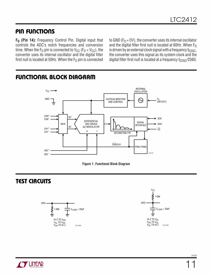
FU CTIO AL BLOCK DIAGRA
UU W
Figure 1. Functional Block Diagram
PI FU CTIO S
UUU
FO (Pin 14): Frequency Control Pin. Digital input thatcontrols the ADC’s notch frequencies and conversiontime. When the FO pin is connected to VCC (FO = VCC), theconverter uses its internal oscillator and the digital filterfirst null is located at 50Hz. When the FO pin is connected
to GND (FO = OV), the converter uses its internal oscillatorand the digital filter first null is located at 60Hz. When FOis driven by an external clock signal with a frequency fEOSC,the converter uses this signal as its system clock and thedigital filter first null is located at a frequency fEOSC/2560.
AUTOCALIBRATIONAND CONTROL
DECIMATING FIR
CH0/CH1
INTERNALOSCILLATOR
SERIALINTERFACE
PING-PONG
DIFFERENTIAL3RD ORDER
∆Σ MODULATOR
+ –
MUX
GND
REF+
CH0+IN+
IN–
CH0–
CH1+
CH1–
REF –
VCC
SCK
SDO
CS
FO(INT/EXT)
2412 FD
1.69k
SDO
2412 TA03
Hi-Z TO VOHVOL TO VOHVOH TO Hi-Z
CLOAD = 20pF
1.69k
SDO
2412 TA04
Hi-Z TO VOLVOH TO VOLVOL TO Hi-Z
CLOAD = 20pF
VCC
LTC2412
122412f
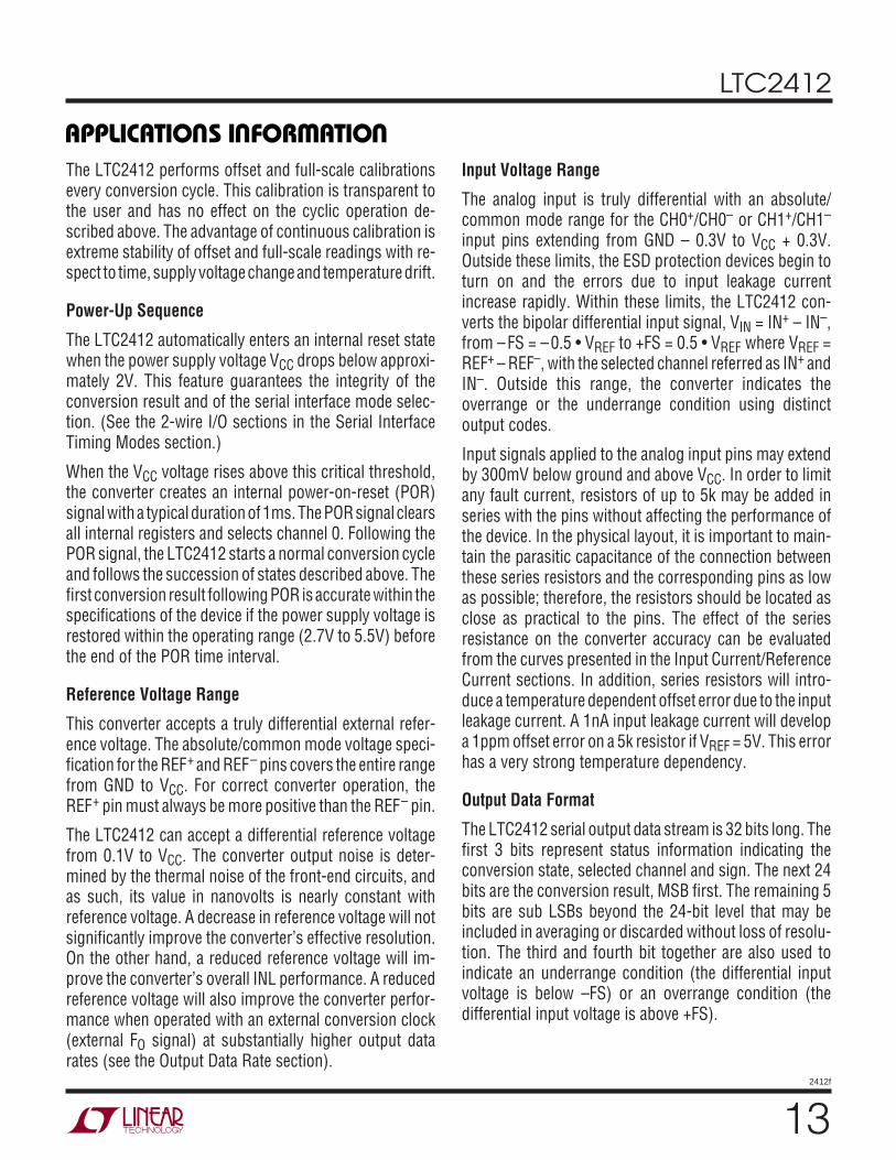
CONVERTER OPERATION
Converter Operation Cycle
The LTC2412 is a low power, ∆Σ ADC with automaticalternate channel selection between the two differentialchannels and an easy-to-use 3-wire serial interface (seeFigure 1). Channel 0 is selected automatically at power upand the two channels are selected alternately afterwards(ping-pong). Its operation is made up of three states. Theconverter operating cycle begins with the conversion,followed by the low power sleep state and ends with thedata output (see Figure 2). The 3-wire interface consistsof serial data output (SDO), serial clock (SCK) and chipselect (CS).
Initially, the LTC2412 performs a conversion. Once theconversion is complete, the device enters the sleep state.The part remains in the sleep state as long as CS is HIGH.While in this sleep state, power consumption is reduced bynearly two orders of magnitude. The conversion result isheld indefinitely in a static shift register while the converteris in the sleep state.
Once CS is pulled LOW, the device exits the low powermode and enters the data output state. If CS is pulled HIGHbefore the first rising edge of SCK, the device returns to thelow power sleep mode and the conversion result is stillheld in the internal static shift register. If CS remains LOW
after the first rising edge of SCK, the device beginsoutputting the conversion result. Taking CS high at thispoint will terminate the data output state and start a newconversion. There is no latency in the conversion result.The data output corresponds to the conversion just per-formed. This result is shifted out on the serial data out pin(SDO) under the control of the serial clock (SCK). Data isupdated on the falling edge of SCK allowing the user toreliably latch data on the rising edge of SCK (see Figure 3).The data output state is concluded once 32 bits are readout of the ADC or when CS is brought HIGH. The deviceautomatically initiates a new conversion and the cyclerepeats.
Through timing control of the CS and SCK pins, theLTC2412 offers several flexible modes of operation(internal or external SCK and free-running conversionmodes). These various modes do not require program-ming configuration registers; moreover, they do not dis-turb the cyclic operation described above. These modes ofoperation are described in detail in the Serial InterfaceTiming Modes section.
Conversion Clock
A major advantage the delta-sigma converter offers overconventional type converters is an on-chip digital filter(commonly implemented as a Sinc or Comb filter). Forhigh resolution, low frequency applications, this filter istypically designed to reject line frequencies of 50Hz or60Hz plus their harmonics. The filter rejection perfor-mance is directly related to the accuracy of the convertersystem clock. The LTC2412 incorporates a highly accu-rate on-chip oscillator. This eliminates the need for exter-nal frequency setting components such as crystals oroscillators. Clocked by the on-chip oscillator, the LTC2412achieves a minimum of 110dB rejection at the line fre-quency (50Hz or 60Hz ±2%).
Ease of Use
The LTC2412 data output has no latency, filter settlingdelay or redundant data associated with the conversioncycle. There is a one-to-one correspondence between theconversion and the output data. Therefore, multiplexingmultiple analog voltages is easy.
APPLICATIO S I FOR ATIO
WU UUFigure 2. LTC2412 State Transition Diagram
CONVERT
POWER UPIN+ = CH0+, IN– = CH0–
SLEEP
DATA OUTPUTSWITCH CHANNEL
2412 F02
TRUE
FALSE CS = LOW ANDSCK
LTC2412
132412f
The LTC2412 performs offset and full-scale calibrationsevery conversion cycle. This calibration is transparent tothe user and has no effect on the cyclic operation de-scribed above. The advantage of continuous calibration isextreme stability of offset and full-scale readings with re-spect to time, supply voltage change and temperature drift.
Power-Up Sequence
The LTC2412 automatically enters an internal reset statewhen the power supply voltage VCC drops below approxi-mately 2V. This feature guarantees the integrity of theconversion result and of the serial interface mode selec-tion. (See the 2-wire I/O sections in the Serial InterfaceTiming Modes section.)
When the VCC voltage rises above this critical threshold,the converter creates an internal power-on-reset (POR)signal with a typical duration of 1ms. The POR signal clearsall internal registers and selects channel 0. Following thePOR signal, the LTC2412 starts a normal conversion cycleand follows the succession of states described above. Thefirst conversion result following POR is accurate within thespecifications of the device if the power supply voltage isrestored within the operating range (2.7V to 5.5V) beforethe end of the POR time interval.
Reference Voltage Range
This converter accepts a truly differential external refer-ence voltage. The absolute/common mode voltage speci-fication for the REF+ and REF– pins covers the entire rangefrom GND to VCC. For correct converter operation, theREF+ pin must always be more positive than the REF– pin.
The LTC2412 can accept a differential reference voltagefrom 0.1V to VCC. The converter output noise is deter-mined by the thermal noise of the front-end circuits, andas such, its value in nanovolts is nearly constant withreference voltage. A decrease in reference voltage will notsignificantly improve the converter’s effective resolution.On the other hand, a reduced reference voltage will im-prove the converter’s overall INL performance. A reducedreference voltage will also improve the converter perfor-mance when operated with an external conversion clock(external FO signal) at substantially higher output datarates (see the Output Data Rate section).
Input Voltage Range
The analog input is truly differential with an absolute/common mode range for the CH0+/CH0– or CH1+/CH1–
input pins extending from GND – 0.3V to VCC + 0.3V.Outside these limits, the ESD protection devices begin toturn on and the errors due to input leakage currentincrease rapidly. Within these limits, the LTC2412 con-verts the bipolar differential input signal, VIN = IN+ – IN–,from –FS = –0.5 • VREF to +FS = 0.5 • VREF where VREF =REF+ – REF–, with the selected channel referred as IN+ andIN–. Outside this range, the converter indicates theoverrange or the underrange condition using distinctoutput codes.
Input signals applied to the analog input pins may extendby 300mV below ground and above VCC. In order to limitany fault current, resistors of up to 5k may be added inseries with the pins without affecting the performance ofthe device. In the physical layout, it is important to main-tain the parasitic capacitance of the connection betweenthese series resistors and the corresponding pins as lowas possible; therefore, the resistors should be located asclose as practical to the pins. The effect of the seriesresistance on the converter accuracy can be evaluatedfrom the curves presented in the Input Current/ReferenceCurrent sections. In addition, series resistors will intro-duce a temperature dependent offset error due to the inputleakage current. A 1nA input leakage current will developa 1ppm offset error on a 5k resistor if VREF = 5V. This errorhas a very strong temperature dependency.
Output Data Format
The LTC2412 serial output data stream is 32 bits long. Thefirst 3 bits represent status information indicating theconversion state, selected channel and sign. The next 24bits are the conversion result, MSB first. The remaining 5bits are sub LSBs beyond the 24-bit level that may beincluded in averaging or discarded without loss of resolu-tion. The third and fourth bit together are also used toindicate an underrange condition (the differential inputvoltage is below –FS) or an overrange condition (thedifferential input voltage is above +FS).
APPLICATIO S I FOR ATIO
WU UU
LTC2412
142412f
Bit 31 (first output bit) is the end of conversion (EOC)indicator. This bit is available at the SDO pin during theconversion and sleep states whenever the CS pin is LOW.This bit is HIGH during the conversion and goes LOWwhen the conversion is complete.
Bit 30 (second output bit) is the selected channel indicator.The bit is LOW for channel 0 and HIGH for channel 1selected.
Bit 29 (third output bit) is the conversion result sign indi-cator (SIG). If VIN is >0, this bit is HIGH. If VIN is <0, thisbit is LOW.
Bit 28 (fourth output bit) is the most significant bit (MSB)of the result. This bit in conjunction with Bit 29 alsoprovides the underrange or overrange indication. If bothBit 29 and Bit 28 are HIGH, the differential input voltage isabove +FS. If both Bit 29 and Bit 28 are LOW, thedifferential input voltage is below –FS.
The function of these bits is summarized in Table 1.Table 1. LTC2412 Status Bits
Bit 31 Bit 30 Bit 29 Bit 28Input Range EOC CH0/CH1 SIG MSB
VIN ≥ 0.5 • VREF 0 0 or 1 1 1
0V ≤ VIN < 0.5 • VREF 0 0 or 1 1 0
–0.5 • VREF ≤ VIN < 0V 0 0 or 1 0 1
VIN < –0.5 • VREF 0 0 or 1 0 0
Bits 28-5 are the 24-bit conversion result MSB first.
Bit 5 is the least significant bit (LSB).
Bits 4-0 are sub LSBs below the 24-bit level. Bits 4-0 maybe included in averaging or discarded without loss ofresolution.
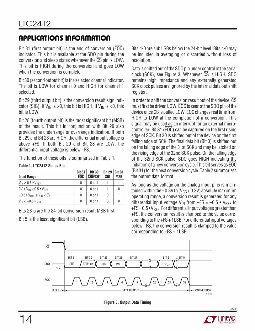
Data is shifted out of the SDO pin under control of the serialclock (SCK), see Figure 3. Whenever CS is HIGH, SDOremains high impedance and any externally generatedSCK clock pulses are ignored by the internal data out shiftregister.
In order to shift the conversion result out of the device, CSmust first be driven LOW. EOC is seen at the SDO pin of thedevice once CS is pulled LOW. EOC changes real time fromHIGH to LOW at the completion of a conversion. Thissignal may be used as an interrupt for an external micro-controller. Bit 31 (EOC) can be captured on the first risingedge of SCK. Bit 30 is shifted out of the device on the firstfalling edge of SCK. The final data bit (Bit 0) is shifted outon the falling edge of the 31st SCK and may be latched onthe rising edge of the 32nd SCK pulse. On the falling edgeof the 32nd SCK pulse, SDO goes HIGH indicating theinitiation of a new conversion cycle. This bit serves as EOC(Bit 31) for the next conversion cycle. Table 2 summarizesthe output data format.
As long as the voltage on the analog input pins is main-tained within the –0.3V to (VCC + 0.3V) absolute maximumoperating range, a conversion result is generated for anydifferential input voltage VIN from –FS = –0.5 • VREF to+FS = 0.5 • VREF. For differential input voltages greater than+FS, the conversion result is clamped to the value corre-sponding to the +FS + 1LSB. For differential input voltagesbelow –FS, the conversion result is clamped to the valuecorresponding to –FS – 1LSB.
APPLICATIO S I FOR ATIO
WU UUFigure 3. Output Data Timing
MSBSIGCH0/CH1
1 2 3 4 5 26 27 32
BIT 0BIT 27 BIT 5
LSB24
BIT 28BIT 29BIT 30
SDO
SCK
CS
EOC
BIT 31
SLEEP DATA OUTPUT CONVERSION2412 F03
Hi-Z
LTC2412
152412f
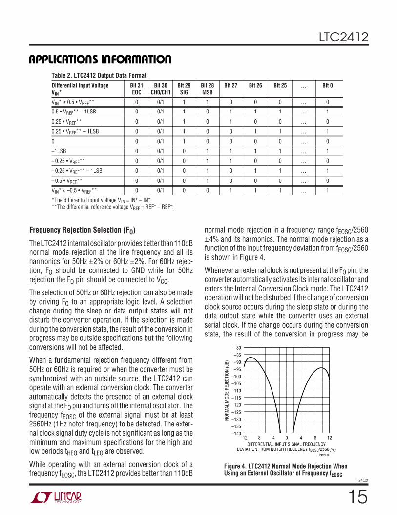
Frequency Rejection Selection (FO)
The LTC2412 internal oscillator provides better than 110dBnormal mode rejection at the line frequency and all itsharmonics for 50Hz ±2% or 60Hz ±2%. For 60Hz rejec-tion, FO should be connected to GND while for 50Hzrejection the FO pin should be connected to VCC.
The selection of 50Hz or 60Hz rejection can also be madeby driving FO to an appropriate logic level. A selectionchange during the sleep or data output states will notdisturb the converter operation. If the selection is madeduring the conversion state, the result of the conversion inprogress may be outside specifications but the followingconversions will not be affected.
When a fundamental rejection frequency different from50Hz or 60Hz is required or when the converter must besynchronized with an outside source, the LTC2412 canoperate with an external conversion clock. The converterautomatically detects the presence of an external clocksignal at the FO pin and turns off the internal oscillator. Thefrequency fEOSC of the external signal must be at least2560Hz (1Hz notch frequency) to be detected. The exter-nal clock signal duty cycle is not significant as long as theminimum and maximum specifications for the high andlow periods tHEO and tLEO are observed.
While operating with an external conversion clock of afrequency fEOSC, the LTC2412 provides better than 110dB
normal mode rejection in a frequency range fEOSC/2560±4% and its harmonics. The normal mode rejection as afunction of the input frequency deviation from fEOSC/2560is shown in Figure 4.
Whenever an external clock is not present at the FO pin, theconverter automatically activates its internal oscillator andenters the Internal Conversion Clock mode. The LTC2412operation will not be disturbed if the change of conversionclock source occurs during the sleep state or during thedata output state while the converter uses an externalserial clock. If the change occurs during the conversionstate, the result of the conversion in progress may be
Figure 4. LTC2412 Normal Mode Rejection WhenUsing an External Oscillator of Frequency fEOSC
APPLICATIO S I FOR ATIO
WU UU
Table 2. LTC2412 Output Data FormatDifferential Input Voltage Bit 31 Bit 30 Bit 29 Bit 28 Bit 27 Bit 26 Bit 25 … Bit 0VIN* EOC CH0/CH1 SIG MSB
VIN* ≥ 0.5 • VREF** 0 0/1 1 1 0 0 0 … 0
0.5 • VREF** – 1LSB 0 0/1 1 0 1 1 1 … 1
0.25 • VREF** 0 0/1 1 0 1 0 0 … 0
0.25 • VREF** – 1LSB 0 0/1 1 0 0 1 1 … 1
0 0 0/1 1 0 0 0 0 … 0
–1LSB 0 0/1 0 1 1 1 1 … 1
– 0.25 • VREF** 0 0/1 0 1 1 0 0 … 0
– 0.25 • VREF** – 1LSB 0 0/1 0 1 0 1 1 … 1
– 0.5 • VREF** 0 0/1 0 1 0 0 0 … 0
VIN* < –0.5 • VREF** 0 0/1 0 0 1 1 1 … 1
*The differential input voltage VIN = IN+ – IN–.**The differential reference voltage VREF = REF+ – REF–.
DIFFERENTIAL INPUT SIGNAL FREQUENCYDEVIATION FROM NOTCH FREQUENCY fEOSC/2560(%)
–12 –8 –4 0 4 8 12
NORM
AL M
ODE
REJE
CTIO
N (d
B)
2412 F04
–80
–85
–90
–95
–100
–105
–110
–115
–120
–125
–130
–135
–140
LTC2412
162412f
APPLICATIO S I FOR ATIO
WU UU
outside specifications but the following conversions willnot be affected. If the change occurs during the data outputstate and the converter is in the Internal SCK mode, theserial clock duty cycle may be affected but the serial datastream will remain valid.
Table 3 summarizes the duration of each state and theachievable output data rate as a function of FO.
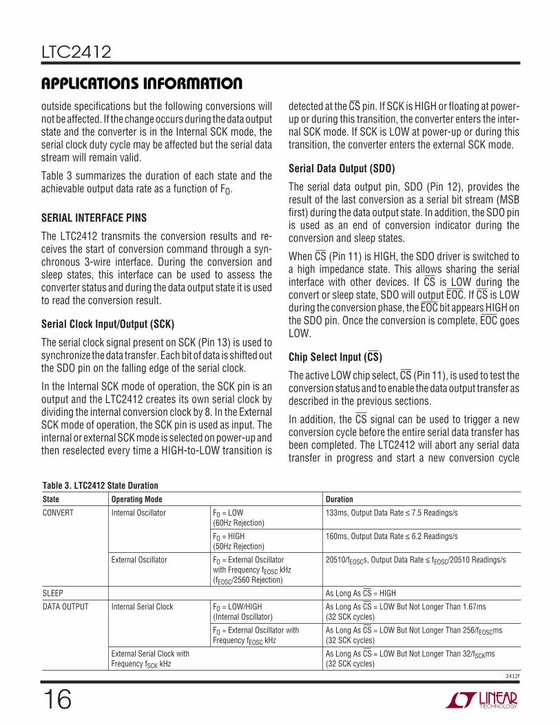
SERIAL INTERFACE PINS
The LTC2412 transmits the conversion results and re-ceives the start of conversion command through a syn-chronous 3-wire interface. During the conversion andsleep states, this interface can be used to assess theconverter status and during the data output state it is usedto read the conversion result.
Serial Clock Input/Output (SCK)
The serial clock signal present on SCK (Pin 13) is used tosynchronize the data transfer. Each bit of data is shifted outthe SDO pin on the falling edge of the serial clock.
In the Internal SCK mode of operation, the SCK pin is anoutput and the LTC2412 creates its own serial clock bydividing the internal conversion clock by 8. In the ExternalSCK mode of operation, the SCK pin is used as input. Theinternal or external SCK mode is selected on power-up andthen reselected every time a HIGH-to-LOW transition is
detected at the CS pin. If SCK is HIGH or floating at power-up or during this transition, the converter enters the inter-nal SCK mode. If SCK is LOW at power-up or during thistransition, the converter enters the external SCK mode.
Serial Data Output (SDO)
The serial data output pin, SDO (Pin 12), provides theresult of the last conversion as a serial bit stream (MSBfirst) during the data output state. In addition, the SDO pinis used as an end of conversion indicator during theconversion and sleep states.
When CS (Pin 11) is HIGH, the SDO driver is switched toa high impedance state. This allows sharing the serialinterface with other devices. If CS is LOW during theconvert or sleep state, SDO will output EOC. If CS is LOWduring the conversion phase, the EOC bit appears HIGH onthe SDO pin. Once the conversion is complete, EOC goesLOW.
Chip Select Input (CS)
The active LOW chip select, CS (Pin 11), is used to test theconversion status and to enable the data output transfer asdescribed in the previous sections.
In addition, the CS signal can be used to trigger a newconversion cycle before the entire serial data transfer hasbeen completed. The LTC2412 will abort any serial datatransfer in progress and start a new conversion cycle
Table 3. LTC2412 State DurationState Operating Mode Duration
CONVERT Internal Oscillator FO = LOW 133ms, Output Data Rate ≤ 7.5 Readings/s(60Hz Rejection)
FO = HIGH 160ms, Output Data Rate ≤ 6.2 Readings/s(50Hz Rejection)
External Oscillator FO = External Oscillator 20510/fEOSCs, Output Data Rate ≤ fEOSC/20510 Readings/swith Frequency fEOSC kHz(fEOSC/2560 Rejection)
SLEEP As Long As CS = HIGH
DATA OUTPUT Internal Serial Clock FO = LOW/HIGH As Long As CS = LOW But Not Longer Than 1.67ms(Internal Oscillator) (32 SCK cycles)
FO = External Oscillator with As Long As CS = LOW But Not Longer Than 256/fEOSCmsFrequency fEOSC kHz (32 SCK cycles)
External Serial Clock with As Long As CS = LOW But Not Longer Than 32/fSCKmsFrequency fSCK kHz (32 SCK cycles)
LTC2412
172412f
APPLICATIO S I FOR ATIO
WU UU
anytime a LOW-to-HIGH transition is detected at the CSpin after the converter has entered the data output state(i.e., after the first rising edge of SCK occurs withCS = LOW).
Finally, CS can be used to control the free-running modesof operation, see Serial Interface Timing Modes section.Grounding CS will force the ADC to continuously convertat the maximum output rate selected by FO.
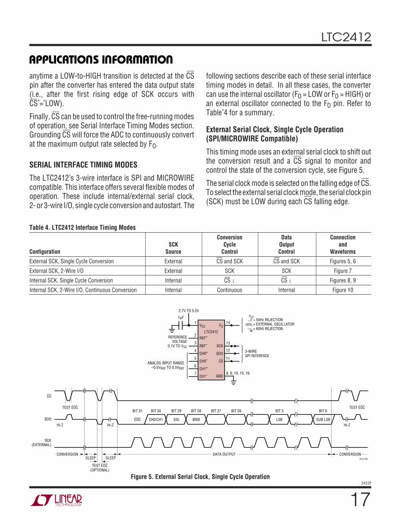
SERIAL INTERFACE TIMING MODES
The LTC2412’s 3-wire interface is SPI and MICROWIREcompatible. This interface offers several flexible modes ofoperation. These include internal/external serial clock,2- or 3-wire I/O, single cycle conversion and autostart. The
following sections describe each of these serial interfacetiming modes in detail. In all these cases, the convertercan use the internal oscillator (FO = LOW or FO = HIGH) oran external oscillator connected to the FO pin. Refer toTable 4 for a summary.
External Serial Clock, Single Cycle Operation(SPI/MICROWIRE Compatible)
This timing mode uses an external serial clock to shift outthe conversion result and a CS signal to monitor andcontrol the state of the conversion cycle, see Figure 5.
The serial clock mode is selected on the falling edge of CS.To select the external serial clock mode, the serial clock pin(SCK) must be LOW during each CS falling edge.
Figure 5. External Serial Clock, Single Cycle Operation
Table 4. LTC2412 Interface Timing ModesConversion Data Connection
SCK Cycle Output andConfiguration Source Control Control Waveforms
External SCK, Single Cycle Conversion External CS and SCK CS and SCK Figures 5, 6
External SCK, 2-Wire I/O External SCK SCK Figure 7
Internal SCK, Single Cycle Conversion Internal CS ↓ CS ↓ Figures 8, 9
Internal SCK, 2-Wire I/O, Continuous Conversion Internal Continuous Internal Figure 10
EOC
BIT 31
SDO
SCK(EXTERNAL)
CS
TEST EOC
SUB LSBMSBSIGCH0/CH1
BIT 0
LSB
BIT 5BIT 27 BIT 26BIT 28BIT 29BIT 30
SLEEPSLEEP
TEST EOC(OPTIONAL)
DATA OUTPUT CONVERSION2412 F05
CONVERSION
Hi-ZHi-ZHi-Z
TEST EOC
= 50Hz REJECTION= EXTERNAL OSCILLATOR= 60Hz REJECTION
VCC
VCC FO
REF+
SCK
CH1+
CH1–
SDO
GND
CS
1 14
2
3 13
6
7
12
8, 9, 10, 15, 16
11
REFERENCEVOLTAGE
0.1V TO VCC
CH0+
CH0–
4
5ANALOG INPUT RANGE
–0.5VREF TO 0.5VREF
1µF
2.7V TO 5.5V
LTC2412
3-WIRESPI INTERFACE
REF–
LTC2412
182412f
APPLICATIO S I FOR ATIO
WU UU
The serial data output pin (SDO) is Hi-Z as long as CS isHIGH. At any time during the conversion cycle, CS may bepulled LOW in order to monitor the state of the converter.While CS is pulled LOW, EOC is output to the SDO pin.EOC = 1 while a conversion is in progress and EOC = 0 ifthe device is in the sleep state. With CS high, the deviceautomatically enters the low power sleep state once theconversion is complete.
When the device is in the sleep state (EOC = 0), itsconversion result is held in an internal static shift regis-ter. Data is shifted out the SDO pin on each falling edge ofSCK. This enables external circuitry to latch the output onthe rising edge of SCK. EOC can be latched on the firstrising edge of SCK and the last bit of the conversion resultcan be latched on the 32nd rising edge of SCK. On the32nd falling edge of SCK, the device begins a new conver-sion. SDO goes HIGH (EOC = 1) indicating a conversion isin progress.
At the conclusion of the data cycle, CS may remain LOWand EOC monitored as an end-of-conversion interrupt.Alternatively, CS may be driven HIGH setting SDO to Hi-Z.
As described above, CS may be pulled LOW at any time inorder to monitor the conversion status.
Typically, CS remains LOW during the data output state.However, the data output state may be aborted by pullingCS HIGH anytime between the first rising edge and the32nd falling edge of SCK, see Figure 6. On the rising edgeof CS, the device aborts the data output state and imme-diately initiates a new conversion. This is useful for sys-tems not requiring all 32 bits of output data, aborting aninvalid conversion cycle or synchronizing the start of aconversion.
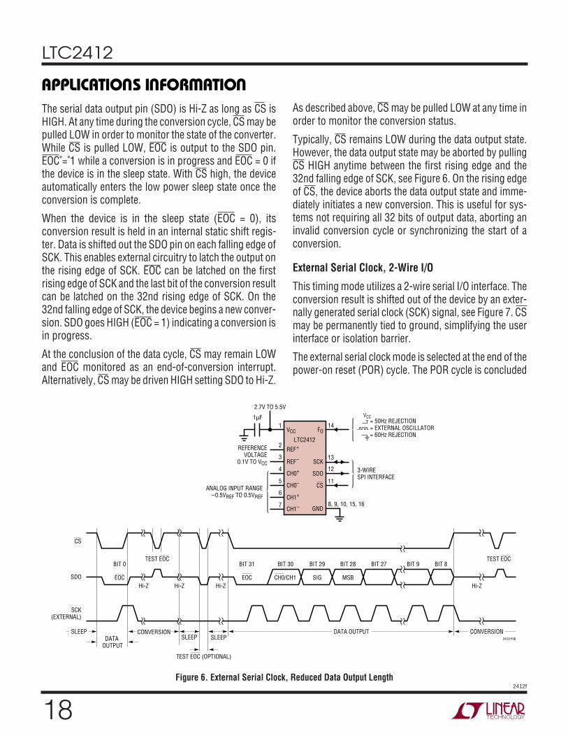
External Serial Clock, 2-Wire I/O
This timing mode utilizes a 2-wire serial I/O interface. Theconversion result is shifted out of the device by an exter-nally generated serial clock (SCK) signal, see Figure 7. CSmay be permanently tied to ground, simplifying the userinterface or isolation barrier.
The external serial clock mode is selected at the end of thepower-on reset (POR) cycle. The POR cycle is concluded
Figure 6. External Serial Clock, Reduced Data Output Length
SDO
SCK(EXTERNAL)
CS
DATA OUTPUT
CONVERSIONSLEEPSLEEP
TEST EOC (OPTIONAL)
TEST EOC
DATA OUTPUT
Hi-Z Hi-ZHi-Z
CONVERSION2412 F06
MSBSIGCH0/CH1
BIT 8BIT 27 BIT 9BIT 28BIT 29BIT 30
EOC
BIT 31BIT 0
EOCHi-Z
TEST EOC
= 50Hz REJECTION= EXTERNAL OSCILLATOR= 60Hz REJECTION
VCC
VCC FO
REF+
SCK
CH1+
CH1–
SDO
GND
CS
1 14
2
3 13
6
7
12
8, 9, 10, 15, 16
11
REFERENCEVOLTAGE
0.1V TO VCC
CH0+
CH0–
4
5ANALOG INPUT RANGE
–0.5VREF TO 0.5VREF
1µF
2.7V TO 5.5V
LTC2412
3-WIRESPI INTERFACE
REF–
SLEEP
LTC2412
192412f
APPLICATIO S I FOR ATIO
WU UU
Figure 7. External Serial Clock, CS = 0 Operation (2-Wire)
EOC
BIT 31
SDO
SCK(EXTERNAL)
CS
MSBSIGCH0/CH1
BIT 0
LSB24
BIT 5BIT 27 BIT 26BIT 28BIT 29BIT 30
DATA OUTPUT CONVERSION2412 F07
CONVERSION
= 50Hz REJECTION= EXTERNAL OSCILLATOR= 60Hz REJECTION
VCC
VCC FO
REF+
SCK
CH1+
CH1–
SDO
GND
CS
1 14
2
3 13
6
7
12
8, 9, 10, 15, 16
11
REFERENCEVOLTAGE
0.1V TO VCC
CH0+
CH0–
4
5ANALOG INPUT RANGE
–0.5VREF TO 0.5VREF
1µF
2.7V TO 5.5V
LTC2412
2-WIREINTERFACE
REF–
typically 1ms after VCC exceeds 2V. The level applied toSCK at this time determines if SCK is internal or external.SCK must be driven LOW prior to the end of POR in orderto enter the external serial clock timing mode.
Since CS is tied LOW, the end-of-conversion (EOC) can becontinuously monitored at the SDO pin during the convertand sleep states. EOC may be used as an interrupt to anexternal controller indicating the conversion result isready. EOC = 1 while the conversion is in progress andEOC = 0 once the conversion ends. On the falling edge ofEOC, the conversion result is loaded into an internal staticshift register. Data is shifted out the SDO pin on eachfalling edge of SCK enabling external circuitry to latch dataon the rising edge of SCK. EOC can be latched on the firstrising edge of SCK. On the 32nd falling edge of SCK, SDOgoes HIGH (EOC = 1) indicating a new conversion hasbegun.
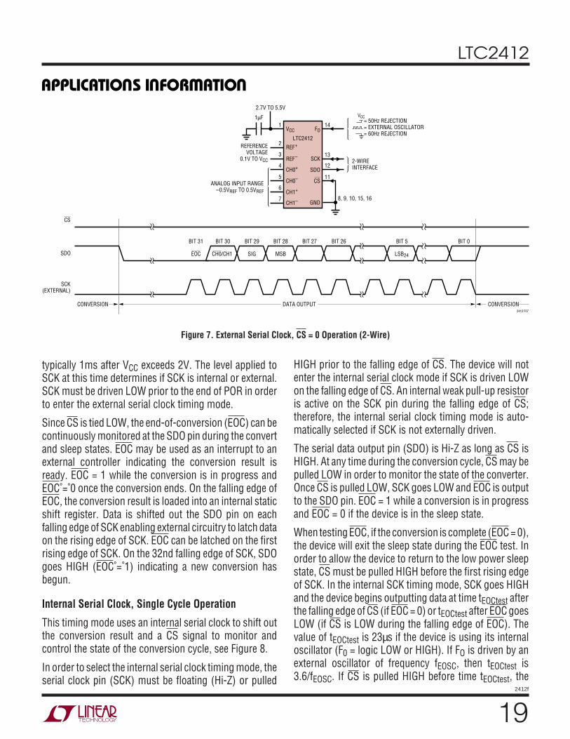
Internal Serial Clock, Single Cycle Operation
This timing mode uses an internal serial clock to shift outthe conversion result and a CS signal to monitor andcontrol the state of the conversion cycle, see Figure 8.
In order to select the internal serial clock timing mode, theserial clock pin (SCK) must be floating (Hi-Z) or pulled
HIGH prior to the falling edge of CS. The device will notenter the internal serial clock mode if SCK is driven LOWon the falling edge of CS. An internal weak pull-up resistoris active on the SCK pin during the falling edge of CS;therefore, the internal serial clock timing mode is auto-matically selected if SCK is not externally driven.
The serial data output pin (SDO) is Hi-Z as long as CS isHIGH. At any time during the conversion cycle, CS may bepulled LOW in order to monitor the state of the converter.Once CS is pulled LOW, SCK goes LOW and EOC is outputto the SDO pin. EOC = 1 while a conversion is in progressand EOC = 0 if the device is in the sleep state.
When testing EOC, if the conversion is complete (EOC = 0),the device will exit the sleep state during the EOC test. Inorder to allow the device to return to the low power sleepstate, CS must be pulled HIGH before the first rising edgeof SCK. In the internal SCK timing mode, SCK goes HIGHand the device begins outputting data at time tEOCtest afterthe falling edge of CS (if EOC = 0) or tEOCtest after EOC goesLOW (if CS is LOW during the falling edge of EOC). Thevalue of tEOCtest is 23µs if the device is using its internaloscillator (F0 = logic LOW or HIGH). If FO is driven by anexternal oscillator of frequency fEOSC, then tEOCtest is3.6/fEOSC. If CS is pulled HIGH before time tEOCtest, the
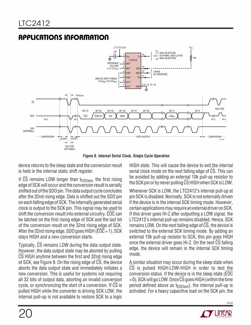
LTC2412
202412f
APPLICATIO S I FOR ATIO
WU UU
device returns to the sleep state and the conversion resultis held in the internal static shift register.
If CS remains LOW longer than tEOCtest, the first risingedge of SCK will occur and the conversion result is seriallyshifted out of the SDO pin. The data output cycle concludesafter the 32nd rising edge. Data is shifted out the SDO pinon each falling edge of SCK. The internally generated serialclock is output to the SCK pin. This signal may be used toshift the conversion result into external circuitry. EOC canbe latched on the first rising edge of SCK and the last bitof the conversion result on the 32nd rising edge of SCK.After the 32nd rising edge, SDO goes HIGH (EOC = 1), SCKstays HIGH and a new conversion starts.
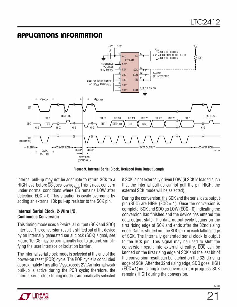
Typically, CS remains LOW during the data output state.However, the data output state may be aborted by pullingCS HIGH anytime between the first and 32nd rising edgeof SCK, see Figure 9. On the rising edge of CS, the deviceaborts the data output state and immediately initiates anew conversion. This is useful for systems not requiringall 32 bits of output data, aborting an invalid conversioncycle, or synchronizing the start of a conversion. If CS ispulled HIGH while the converter is driving SCK LOW, theinternal pull-up is not available to restore SCK to a logic
HIGH state. This will cause the device to exit the internalserial clock mode on the next falling edge of CS. This canbe avoided by adding an external 10k pull-up resistor tothe SCK pin or by never pulling CS HIGH when SCK is LOW.
Whenever SCK is LOW, the LTC2412’s internal pull-up atpin SCK is disabled. Normally, SCK is not externally drivenif the device is in the internal SCK timing mode. However,certain applications may require an external driver on SCK.If this driver goes Hi-Z after outputting a LOW signal, theLTC2412’s internal pull-up remains disabled. Hence, SCKremains LOW. On the next falling edge of CS, the device isswitched to the external SCK timing mode. By adding anexternal 10k pull-up resistor to SCK, this pin goes HIGHonce the external driver goes Hi-Z. On the next CS fallingedge, the device will remain in the internal SCK timingmode.
A similar situation may occur during the sleep state whenCS is pulsed HIGH-LOW-HIGH in order to test theconversion status. If the device is in the sleep state (EOC= 0), SCK will go LOW. Once CS goes HIGH (within the timeperiod defined above as tEOCtest), the internal pull-up isactivated. For a heavy capacitive load on the SCK pin, the
Figure 8. Internal Serial Clock, Single Cycle Operation
SDO
SCK(INTERNAL)
CS
MSBSIGCH0/CH1
BIT 0
LSB24
BIT 5TEST EOC
BIT 27 BIT 26BIT 28BIT 29BIT 30
EOC
BIT 31
SLEEPDATA OUTPUT CONVERSIONCONVERSION
2412 F08
<tEOCtest
VCC
10k
Hi-Z Hi-Z Hi-Z Hi-Z
TEST EOC(OPTIONAL)
= 50Hz REJECTION= EXTERNAL OSCILLATOR= 60Hz REJECTION
VCC
VCC FO
REF+
SCK
CH1+
CH1–
SDO
GND
CS
1 14
2
3 13
6
7
12
8, 9, 10, 15, 16
11
REFERENCEVOLTAGE
0.1V TO VCC
CH0+
CH0–
4
5ANALOG INPUT RANGE
–0.5VREF TO 0.5VREF
1µF
2.7V TO 5.5V
LTC2412
3-WIRESPI INTERFACE
REF–
SLEEP
LTC2412
212412f
APPLICATIO S I FOR ATIO
WU UU
internal pull-up may not be adequate to return SCK to aHIGH level before CS goes low again. This is not a concernunder normal conditions where CS remains LOW afterdetecting EOC = 0. This situation is easily overcome byadding an external 10k pull-up resistor to the SCK pin.
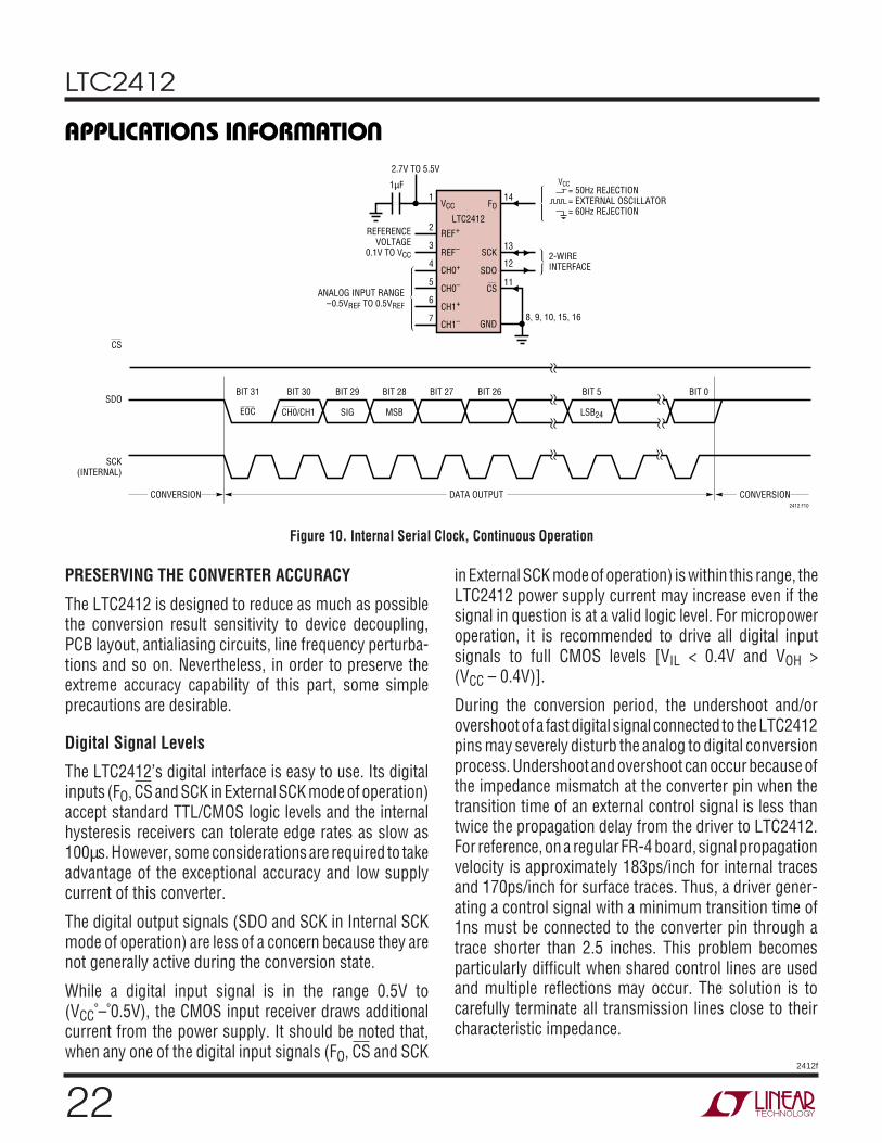
Internal Serial Clock, 2-Wire I/O,Continuous Conversion
This timing mode uses a 2-wire, all output (SCK and SDO)interface. The conversion result is shifted out of the deviceby an internally generated serial clock (SCK) signal, seeFigure 10. CS may be permanently tied to ground, simpli-fying the user interface or isolation barrier.
The internal serial clock mode is selected at the end of thepower-on reset (POR) cycle. The POR cycle is concludedapproximately 1ms after VCC exceeds 2V. An internal weakpull-up is active during the POR cycle; therefore, theinternal serial clock timing mode is automatically selected
if SCK is not externally driven LOW (if SCK is loaded suchthat the internal pull-up cannot pull the pin HIGH, theexternal SCK mode will be selected).
During the conversion, the SCK and the serial data outputpin (SDO) are HIGH (EOC = 1). Once the conversion iscomplete, SCK and SDO go LOW (EOC = 0) indicating theconversion has finished and the device has entered thedata output state. The data output cycle begins on thefirst rising edge of SCK and ends after the 32nd risingedge. Data is shifted out the SDO pin on each falling edgeof SCK. The internally generated serial clock is outputto the SCK pin. This signal may be used to shift theconversion result into external circuitry. EOC can belatched on the first rising edge of SCK and the last bit ofthe conversion result can be latched on the 32nd risingedge of SCK. After the 32nd rising edge, SDO goes HIGH(EOC = 1) indicating a new conversion is in progress. SCKremains HIGH during the conversion.
Figure 9. Internal Serial Clock, Reduced Data Output Length
SDO
SCK(INTERNAL)
CS
> tEOCtest
MSBSIGCH0/CH1
BIT 8TEST EOC
BIT 27 BIT 26BIT 28BIT 29BIT 30
EOC
BIT 31
EOC
BIT 0
DATA OUTPUT
Hi-Z Hi-Z Hi-Z Hi-Z Hi-Z
DATAOUTPUT
CONVERSIONCONVERSIONSLEEP2412 F09
<tEOCtest
VCC
10k
TEST EOC(OPTIONAL)
TEST EOC
= 50Hz REJECTION= EXTERNAL OSCILLATOR= 60Hz REJECTION
VCC
VCC FO
REF+
SCK
CH1+
CH1–
SDO
GND
CS
1 14
2
3 13
6
7
12
8, 9, 10, 15, 16
11
REFERENCEVOLTAGE
0.1V TO VCC
CH0+
CH0–
4
5ANALOG INPUT RANGE
–0.5VREF TO 0.5VREF
1µF
2.7V TO 5.5V
LTC2412
3-WIRESPI INTERFACE
REF–
SLEEP SLEEP
LTC2412
222412f
APPLICATIO S I FOR ATIO
WU UU
PRESERVING THE CONVERTER ACCURACY
The LTC2412 is designed to reduce as much as possiblethe conversion result sensitivity to device decoupling,PCB layout, antialiasing circuits, line frequency perturba-tions and so on. Nevertheless, in order to preserve theextreme accuracy capability of this part, some simpleprecautions are desirable.
Digital Signal Levels
The LTC2412’s digital interface is easy to use. Its digitalinputs (FO, CS and SCK in External SCK mode of operation)accept standard TTL/CMOS logic levels and the internalhysteresis receivers can tolerate edge rates as slow as100µs. However, some considerations are required to takeadvantage of the exceptional accuracy and low supplycurrent of this converter.
The digital output signals (SDO and SCK in Internal SCKmode of operation) are less of a concern because they arenot generally active during the conversion state.
While a digital input signal is in the range 0.5V to(VCC – 0.5V), the CMOS input receiver draws additionalcurrent from the power supply. It should be noted that,when any one of the digital input signals (FO, CS and SCK
in External SCK mode of operation) is within this range, theLTC2412 power supply current may increase even if thesignal in question is at a valid logic level. For micropoweroperation, it is recommended to drive all digital inputsignals to full CMOS levels [VIL < 0.4V and VOH >(VCC – 0.4V)].
During the conversion period, the undershoot and/orovershoot of a fast digital signal connected to the LTC2412pins may severely disturb the analog to digital conversionprocess. Undershoot and overshoot can occur because ofthe impedance mismatch at the converter pin when thetransition time of an external control signal is less thantwice the propagation delay from the driver to LTC2412.For reference, on a regular FR-4 board, signal propagationvelocity is approximately 183ps/inch for internal tracesand 170ps/inch for surface traces. Thus, a driver gener-ating a control signal with a minimum transition time of1ns must be connected to the converter pin through atrace shorter than 2.5 inches. This problem becomesparticularly difficult when shared control lines are usedand multiple reflections may occur. The solution is tocarefully terminate all transmission lines close to theircharacteristic impedance.
Figure 10. Internal Serial Clock, Continuous Operation
SDO
SCK(INTERNAL)
CS
LSB24MSBSIGCH0/CH1
BIT 5 BIT 0BIT 27 BIT 26BIT 28BIT 29BIT 30
EOC
BIT 31
DATA OUTPUT CONVERSIONCONVERSION2412 F10
= 50Hz REJECTION= EXTERNAL OSCILLATOR= 60Hz REJECTION
VCC
VCC FO
REF+
SCK
CH1+
CH1–
SDO
GND
CS
1 14
2
3 13
6
7
12
8, 9, 10, 15, 16
11
REFERENCEVOLTAGE
0.1V TO VCC
CH0+
CH0–
4
5ANALOG INPUT RANGE
–0.5VREF TO 0.5VREF
1µF
2.7V TO 5.5V
LTC2412
2-WIREINTERFACE
REF–
LTC2412
232412f
APPLICATIO S I FOR ATIO
WU UU
Parallel termination near the LTC2412 pin will eliminatethis problem but will increase the driver power dissipation.A series resistor between 27Ω and 56Ω placed near thedriver or near the LTC2412 pin will also eliminate thisproblem without additional power dissipation. The actualresistor value depends upon the trace impedance andconnection topology.
An alternate solution is to reduce the edge rate of thecontrol signals. It should be noted that using very slowedges will increase the converter power supply currentduring the transition time. The multiple ground pins usedin this package configuration, as well as the differentialinput and reference architecture, reduce substantially theconverter’s sensitivity to ground currents.
Particular attention must be given to the connection of theFO signal when the LTC2412 is used with an externalconversion clock. This clock is active during the conver-sion time and the normal mode rejection provided by theinternal digital filter is not very high at this frequency. Anormal mode signal of this frequency at the converterreference terminals may result into DC gain and INLerrors. A normal mode signal of this frequency at theconverter input terminals may result into a DC offset error.
Such perturbations may occur due to asymmetric capaci-tive coupling between the FO signal trace and the converterinput and/or reference connection traces. An immediatesolution is to maintain maximum possible separationbetween the FO signal trace and the input/reference sig-nals. When the FO signal is parallel terminated near theconverter, substantial AC current is flowing in the loopformed by the FO connection trace, the termination and theground return path. Thus, perturbation signals may beinductively coupled into the converter input and/or refer-ence. In this situation, the user must reduce to a minimumthe loop area for the FO signal as well as the loop area forthe differential input and reference connections.
Driving the Input and Reference
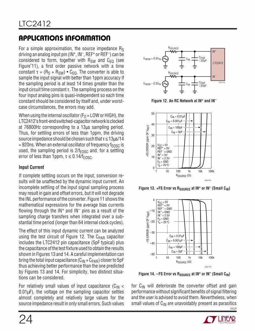
The input and reference pins of the LTC2412 converter aredirectly connected to a network of sampling capacitors.Depending upon the relation between the differential inputvoltage and the differential reference voltage, these ca-pacitors are switching between these four pins transferingsmall amounts of charge in the process. A simplifiedequivalent circuit is shown in Figure 11, where IN+ and IN–
refer to the selected differential channel and the unselectedchannel is omitted for simplicity.
VREF+
VIN+
VCC
RSW (TYP)20k
ILEAK
ILEAK
VCC
ILEAK
ILEAK
VCC
RSW (TYP)20k
CEQ18pF(TYP)
RSW (TYP)20k
ILEAK
IIN+
VIN–
IIN–
IREF+
IREF–
2412 F11
ILEAK
VCC
ILEAK
ILEAK
SWITCHING FREQUENCYfSW = 76800Hz INTERNAL OSCILLATOR (FO = LOW OR HIGH)fSW = 0.5 • fEOSC EXTERNAL OSCILLATOR
VREF–
RSW (TYP)20k
I INV V V
R
I INV V V
R
I REFV V V
RV
V R
I REFV V V
RV
V Rwhere
AVGIN INCM REFCM
EQ
AVGIN INCM REFCM
EQ
AVGREF INCM REFCM
EQ
IN
REF EQ
AVGREF INCM REFCM
EQ
IN
REF EQ
+
−
+
−
( ) = + −•
( ) = − + −•
( ) = • − +•
−•
( ) = − • − +•
+•
0 5
0 5
1 50 5
1 50 5
2
2
.
.
..
..
::
.
.
. /
V REF REF
VREF REF
V IN IN
VIN IN
R M INTERNAL OSCILLATOR Hz Notch F LOW
R M INTERNAL OSCILLATOR Hz Notch F HIGH
R f EXTERNAL OSCILLATOR
REF
REFCM
IN
INCM
EQ O
EQ O
EQ EOSC
= −
= +
= −
= −
= =( )= =( )= •( )
+ −
+ −
+ −
+ −
2
2
3 61 60
4 32 50
0 555 1012
Ω
Ω
Figure 11. LTC2412 Equivalent Analog Input Circuit
LTC2412
242412f
APPLICATIO S I FOR ATIO
WU UU
For a simple approximation, the source impedance RSdriving an analog input pin (IN+, IN–, REF+ or REF–) can beconsidered to form, together with RSW and CEQ (seeFigure 11), a first order passive network with a timeconstant τ = (RS + RSW) • CEQ. The converter is able tosample the input signal with better than 1ppm accuracy ifthe sampling period is at least 14 times greater than theinput circuit time constant τ. The sampling process on thefour input analog pins is quasi-independent so each timeconstant should be considered by itself and, under worst-case circumstances, the errors may add.
When using the internal oscillator (FO = LOW or HIGH), theLTC2412’s front-end switched-capacitor network is clockedat 76800Hz corresponding to a 13µs sampling period.Thus, for settling errors of less than 1ppm, the drivingsource impedance should be chosen such that τ ≤ 13µs/14= 920ns. When an external oscillator of frequency fEOSC isused, the sampling period is 2/fEOSC and, for a settlingerror of less than 1ppm, τ ≤ 0.14/fEOSC.
Input Current
If complete settling occurs on the input, conversion re-sults will be unaffected by the dynamic input current. Anincomplete settling of the input signal sampling processmay result in gain and offset errors, but it will not degradethe INL performance of the converter. Figure 11 shows themathematical expressions for the average bias currentsflowing through the IN+ and IN– pins as a result of thesampling charge transfers when integrated over a sub-stantial time period (longer than 64 internal clock cycles).
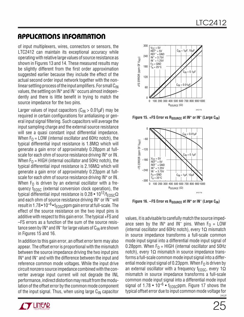
The effect of this input dynamic current can be analyzedusing the test circuit of Figure 12. The CPAR capacitorincludes the LTC2412 pin capacitance (5pF typical) plusthe capacitance of the test fixture used to obtain the resultsshown in Figures 13 and 14. A careful implementation canbring the total input capacitance (CIN + CPAR) closer to 5pFthus achieving better performance than the one predictedby Figures 13 and 14. For simplicity, two distinct situa-tions can be considered.
For relatively small values of input capacitance (CIN <0.01µF), the voltage on the sampling capacitor settlesalmost completely and relatively large values for thesource impedance result in only small errors. Such values
CIN
2412 F12
VINCM + 0.5VIN
RSOURCEIN+
LTC2412
CPAR≅20pF
CINVINCM – 0.5VIN
RSOURCEIN –
CPAR≅20pF
Figure 12. An RC Network at IN+ and IN–
Figure 14. –FS Error vs RSOURCE at IN+ or IN– (Small CIN)
Figure 13. +FS Error vs RSOURCE at IN+ or IN– (Small CIN)
RSOURCE (Ω)1 10 100 1k 10k 100k
+FS
ERRO
R (p
pm O
F V R
EF)
2412 F13
50
40
30
20
10
0
VCC = 5VREF+ = 5VREF – = GNDIN+ = 5VIN– = 2.5VFO = GNDTA = 25°C
CIN = 0.01µF
CIN = 0.001µF
CIN = 100pFCIN = 0pF
RSOURCE (Ω)1 10 100 1k 10k 100k
–FS
ERRO
R (p
pm O
F V R
EF)
2412 F14
0
–10
–20
–30
–40
–50
VCC = 5VREF+ = 5VREF – = GNDIN+ = GNDIN– = 2.5VFO = GNDTA = 25°C
CIN = 0.01µF
CIN = 0.001µF
CIN = 100pFCIN = 0pF
for CIN will deteriorate the converter offset and gainperformance without significant benefits of signal filteringand the user is advised to avoid them. Nevertheless, whensmall values of CIN are unavoidably present as parasitics
LTC2412
252412f
APPLICATIO S I FOR ATIO
WU UU
of input multiplexers, wires, connectors or sensors, theLTC2412 can maintain its exceptional accuracy whileoperating with relative large values of source resistance asshown in Figures 13 and 14. These measured results maybe slightly different from the first order approximationsuggested earlier because they include the effect of theactual second order input network together with the non-linear settling process of the input amplifiers. For small CINvalues, the settling on IN+ and IN– occurs almost indepen-dently and there is little benefit in trying to match thesource impedance for the two pins.
Larger values of input capacitors (CIN > 0.01µF) may berequired in certain configurations for antialiasing or gen-eral input signal filtering. Such capacitors will average theinput sampling charge and the external source resistancewill see a quasi constant input differential impedance.When FO = LOW (internal oscillator and 60Hz notch), thetypical differential input resistance is 1.8MΩ which willgenerate a gain error of approximately 0.28ppm at full-scale for each ohm of source resistance driving IN+ or IN.When FO = HIGH (internal oscillator and 50Hz notch), thetypical differential input resistance is 2.16MΩ which willgenerate a gain error of approximately 0.23ppm at full-scale for each ohm of source resistance driving IN+ or IN.When FO is driven by an external oscillator with a fre-quency fEOSC (external conversion clock operation), thetypical differential input resistance is 0.28 • 1012/fEOSCΩand each ohm of source resistance driving IN+ or IN– willresult in 1.78 • 10–6 • fEOSCppm gain error at full-scale. Theeffect of the source resistance on the two input pins isadditive with respect to this gain error. The typical +FS and–FS errors as a function of the sum of the source resis-tance seen by IN+ and IN– for large values of CIN are shownin Figures 15 and 16.
In addition to this gain error, an offset error term may alsoappear. The offset error is proportional with the mismatchbetween the source impedance driving the two input pinsIN+ and IN– and with the difference between the input andreference common mode voltages. While the input drivecircuit nonzero source impedance combined with the con-verter average input current will not degrade the INLperformance, indirect distortion may result from the modu-lation of the offset error by the common mode componentof the input signal. Thus, when using large CIN capacitor
values, it is advisable to carefully match the source imped-ance seen by the IN+ and IN– pins. When FO = LOW(internal oscillator and 60Hz notch), every 1Ω mismatchin source impedance transforms a full-scale commonmode input signal into a differential mode input signal of0.28ppm. When FO = HIGH (internal oscillator and 50Hznotch), every 1Ω mismatch in source impedance trans-forms a full-scale common mode input signal into a differ-ential mode input signal of 0.23ppm. When FO is driven byan external oscillator with a frequency fEOSC, every 1Ωmismatch in source impedance transforms a full-scalecommon mode input signal into a differential mode inputsignal of 1.78 • 10–6 • fEOSCppm. Figure 17 shows thetypical offset error due to input common mode voltage for
Figure 15. +FS Error vs RSOURCE at IN+ or IN– (Large CIN)
Figure 16. –FS Error vs RSOURCE at IN+ or IN– (Large CIN)
RSOURCE (Ω)0 100 200 300 400 500 600 700 800 900 1000
+FS
ERRO
R (p
pm O
F V R
EF)
2412 F15
300
240
180
120
60
0
VCC = 5VREF+ = 5VREF – = GNDIN+ = 3.75VIN– = 1.25VFO = GNDTA = 25°C
CIN = 0.01µF
CIN = 0.1µF
CIN = 1µF, 10µF
RSOURCE (Ω)0 100 200 300 400 500 600 700 800 900 1000
–FS
ERRO
R (p
pm O
F V R
EF)
2412 F16
0
–60
–120
–180
–240
–300
VCC = 5VREF+ = 5VREF – = GNDIN+ = 1.25VIN– = 3.75VFO = GNDTA = 25°C
CIN = 0.01µF
CIN = 0.1µF
CIN = 1µF, 10µF
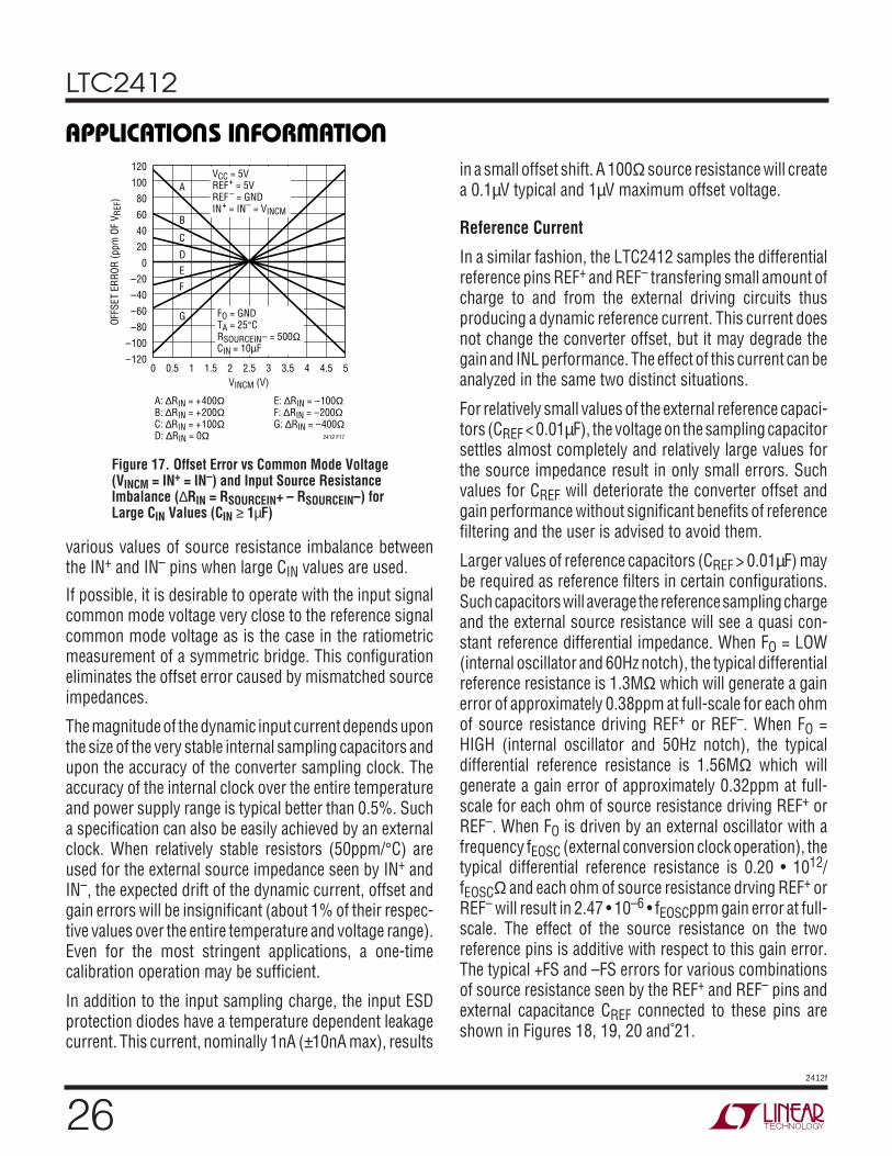
LTC2412
262412f
APPLICATIO S I FOR ATIO
WU UU
various values of source resistance imbalance betweenthe IN+ and IN– pins when large CIN values are used.
If possible, it is desirable to operate with the input signalcommon mode voltage very close to the reference signalcommon mode voltage as is the case in the ratiometricmeasurement of a symmetric bridge. This configurationeliminates the offset error caused by mismatched sourceimpedances.
The magnitude of the dynamic input current depends uponthe size of the very stable internal sampling capacitors andupon the accuracy of the converter sampling clock. Theaccuracy of the internal clock over the entire temperatureand power supply range is typical better than 0.5%. Sucha specification can also be easily achieved by an externalclock. When relatively stable resistors (50ppm/°C) areused for the external source impedance seen by IN+ andIN–, the expected drift of the dynamic current, offset andgain errors will be insignificant (about 1% of their respec-tive values over the entire temperature and voltage range).Even for the most stringent applications, a one-timecalibration operation may be sufficient.
In addition to the input sampling charge, the input ESDprotection diodes have a temperature dependent leakagecurrent. This current, nominally 1nA (±10nA max), results
in a small offset shift. A 100Ω source resistance will createa 0.1µV typical and 1µV maximum offset voltage.
Reference Current
In a similar fashion, the LTC2412 samples the differentialreference pins REF+ and REF– transfering small amount ofcharge to and from the external driving circuits thusproducing a dynamic reference current. This current doesnot change the converter offset, but it may degrade thegain and INL performance. The effect of this current can beanalyzed in the same two distinct situations.
For relatively small values of the external reference capaci-tors (CREF < 0.01µF), the voltage on the sampling capacitorsettles almost completely and relatively large values forthe source impedance result in only small errors. Suchvalues for CREF will deteriorate the converter offset andgain performance without significant benefits of referencefiltering and the user is advised to avoid them.
Larger values of reference capacitors (CREF > 0.01µF) maybe required as reference filters in certain configurations.Such capacitors will average the reference sampling chargeand the external source resistance will see a quasi con-stant reference differential impedance. When FO = LOW(internal oscillator and 60Hz notch), the typical differentialreference resistance is 1.3MΩ which will generate a gainerror of approximately 0.38ppm at full-scale for each ohmof source resistance driving REF+ or REF–. When FO =HIGH (internal oscillator and 50Hz notch), the typicaldifferential reference resistance is 1.56MΩ which willgenerate a gain error of approximately 0.32ppm at full-scale for each ohm of source resistance driving REF+ orREF–. When FO is driven by an external oscillator with afrequency fEOSC (external conversion clock operation), thetypical differential reference resistance is 0.20 • 1012/fEOSCΩ and each ohm of source resistance drving REF+ orREF– will result in 2.47 • 10–6 • fEOSCppm gain error at full-scale. The effect of the source resistance on the tworeference pins is additive with respect to this gain error.The typical +FS and –FS errors for various combinationsof source resistance seen by the REF+ and REF– pins andexternal capacitance CREF connected to these pins areshown in Figures 18, 19, 20 and 21.
Figure 17. Offset Error vs Common Mode Voltage(VINCM = IN+ = IN–) and Input Source ResistanceImbalance (∆RIN = RSOURCEIN+ – RSOURCEIN–) forLarge CIN Values (CIN ≥ 1µF)
VINCM (V)0 0.5 1 1.5 2 2.5 3 3.5 4 4.5 5
OFFS
ET E
RROR
(ppm
OF
V REF
)
2412 F17
120
100
80
60
40
20
0
–20
–40
–60
–80
–100
–120
FO = GNDTA = 25°CRSOURCEIN– = 500ΩCIN = 10µF
VCC = 5VREF+ = 5VREF – = GNDIN+ = IN– = VINCM
A: ∆RIN = +400ΩB: ∆RIN = +200ΩC: ∆RIN = +100ΩD: ∆RIN = 0Ω
E: ∆RIN = –100ΩF: ∆RIN = –200ΩG: ∆RIN = –400Ω
A
B
C
DE
F
G
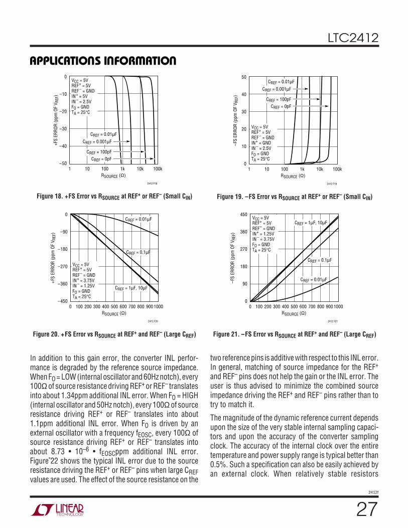
LTC2412
272412f
APPLICATIO S I FOR ATIO
WU UU
In addition to this gain error, the converter INL perfor-mance is degraded by the reference source impedance.When FO = LOW (internal oscillator and 60Hz notch), every100Ω of source resistance driving REF+ or REF– translatesinto about 1.34ppm additional INL error. When FO = HIGH(internal oscillator and 50Hz notch), every 100Ω of sourceresistance driving REF+ or REF– translates into about1.1ppm additional INL error. When FO is driven by anexternal oscillator with a frequency fEOSC, every 100Ω ofsource resistance driving REF+ or REF– translates intoabout 8.73 • 10–6 • fEOSCppm additional INL error.Figure 22 shows the typical INL error due to the sourceresistance driving the REF+ or REF– pins when large CREFvalues are used. The effect of the source resistance on the
two reference pins is additive with respect to this INL error.In general, matching of source impedance for the REF+
and REF– pins does not help the gain or the INL error. Theuser is thus advised to minimize the combined sourceimpedance driving the REF+ and REF– pins rather than totry to match it.
The magnitude of the dynamic reference current dependsupon the size of the very stable internal sampling capaci-tors and upon the accuracy of the converter samplingclock. The accuracy of the internal clock over the entiretemperature and power supply range is typical better than0.5%. Such a specification can also be easily achieved byan external clock. When relatively stable resistors
Figure 18. +FS Error vs RSOURCE at REF+ or REF– (Small CIN) Figure 19. –FS Error vs RSOURCE at REF+ or REF– (Small CIN)
Figure 20. +FS Error vs RSOURCE at REF+ and REF– (Large CREF) Figure 21. –FS Error vs RSOURCE at REF+ and REF– (Large CREF)
RSOURCE (Ω)1 10 100 1k 10k 100k
+FS
ERRO
R (p
pm O
F V R
EF)
2412 F18
0
–10
–20
–30
–40
–50
VCC = 5VREF+ = 5VREF – = GNDIN+ = 5VIN – = 2.5VFO = GNDTA = 25°C
CREF = 0.01µF
CREF = 0.001µF
CREF = 100pFCREF = 0pF
RSOURCE (Ω)1 10 100 1k 10k 100k
–FS
ERRO
R (p
pm O
F V R
EF)
2412 F19
50
40
30
20
10
0
VCC = 5VREF+ = 5VREF – = GNDIN+ = GNDIN – = 2.5VFO = GNDTA = 25°C
CREF = 0.01µF
CREF = 0.001µF
CREF = 100pFCREF = 0pF
RSOURCE (Ω)0 100 200 300 400 500 600 700 800 900 1000
+FS
ERRO
R (p
pm O
F V R
EF)
2412 F20
0
–90
–180
–270
–360
–450
VCC = 5VREF+ = 5VREF– = GNDIN+ = 3.75VIN – = 1.25VFO = GNDTA = 25°C
CREF = 0.01µF
CREF = 0.1µF
CREF = 1µF, 10µF
RSOURCE (Ω)0 100 200 300 400 500 600 700 800 900 1000
–FS
ERRO
R (p
pm O
F V R
EF)
2412 F21
450
360
270
180
90
0
VCC = 5VREF+ = 5VREF– = GNDIN+ = 1.25VIN – = 3.75VFO = GNDTA = 25°C
CREF = 0.01µF
CREF = 0.1µF
CREF = 1µF, 10µF
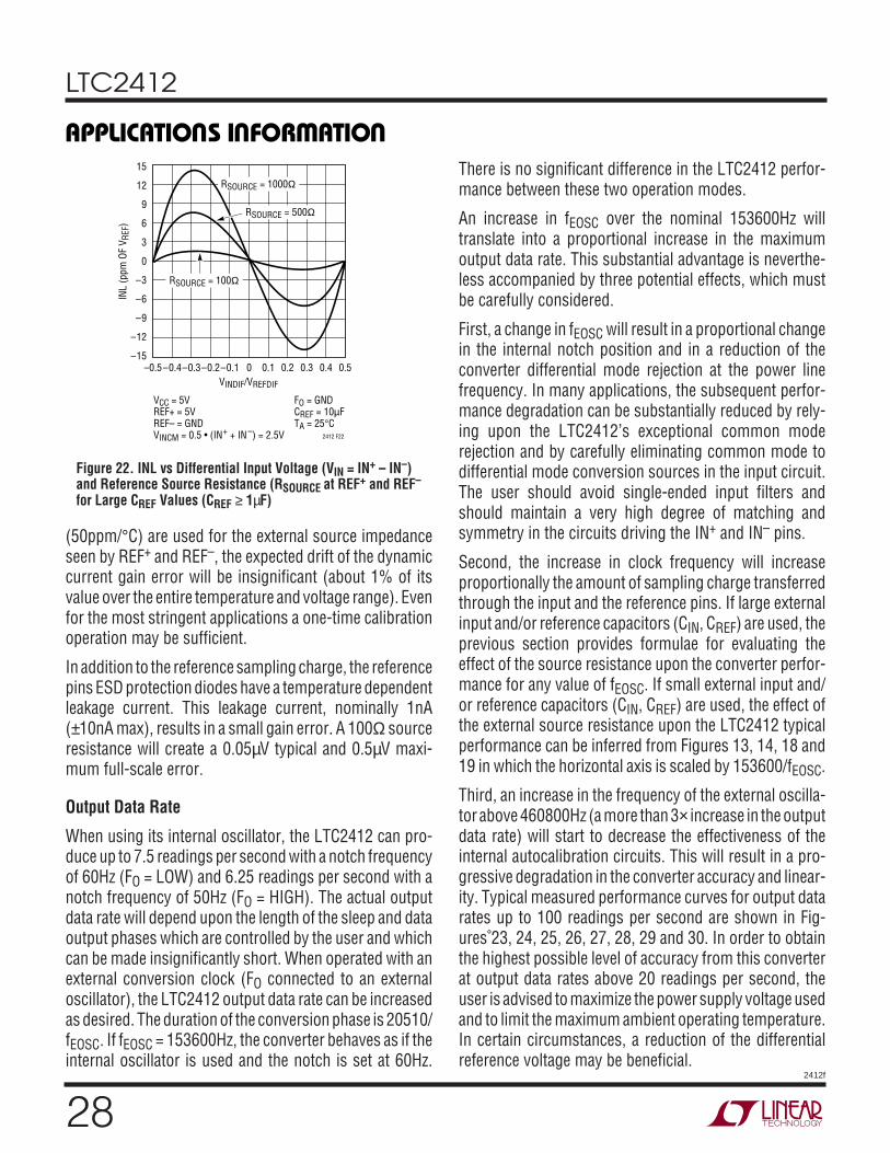
LTC2412
282412f
APPLICATIO S I FOR ATIO
WU UU
(50ppm/°C) are used for the external source impedanceseen by REF+ and REF–, the expected drift of the dynamiccurrent gain error will be insignificant (about 1% of itsvalue over the entire temperature and voltage range). Evenfor the most stringent applications a one-time calibrationoperation may be sufficient.
In addition to the reference sampling charge, the referencepins ESD protection diodes have a temperature dependentleakage current. This leakage current, nominally 1nA(±10nA max), results in a small gain error. A 100Ω sourceresistance will create a 0.05µV typical and 0.5µV maxi-mum full-scale error.
Output Data Rate
When using its internal oscillator, the LTC2412 can pro-duce up to 7.5 readings per second with a notch frequencyof 60Hz (FO = LOW) and 6.25 readings per second with anotch frequency of 50Hz (FO = HIGH). The actual outputdata rate will depend upon the length of the sleep and dataoutput phases which are controlled by the user and whichcan be made insignificantly short. When operated with anexternal conversion clock (FO connected to an externaloscillator), the LTC2412 output data rate can be increasedas desired. The duration of the conversion phase is 20510/fEOSC. If fEOSC = 153600Hz, the converter behaves as if theinternal oscillator is used and the notch is set at 60Hz.
There is no significant difference in the LTC2412 perfor-mance between these two operation modes.
An increase in fEOSC over the nominal 153600Hz willtranslate into a proportional increase in the maximumoutput data rate. This substantial advantage is neverthe-less accompanied by three potential effects, which mustbe carefully considered.
First, a change in fEOSC will result in a proportional changein the internal notch position and in a reduction of theconverter differential mode rejection at the power linefrequency. In many applications, the subsequent perfor-mance degradation can be substantially reduced by rely-ing upon the LTC2412’s exceptional common moderejection and by carefully eliminating common mode todifferential mode conversion sources in the input circuit.The user should avoid single-ended input filters andshould maintain a very high degree of matching andsymmetry in the circuits driving the IN+ and IN– pins.
Second, the increase in clock frequency will increaseproportionally the amount of sampling charge transferredthrough the input and the reference pins. If large externalinput and/or reference capacitors (CIN, CREF) are used, theprevious section provides formulae for evaluating theeffect of the source resistance upon the converter perfor-mance for any value of fEOSC. If small external input and/or reference capacitors (CIN, CREF) are used, the effect ofthe external source resistance upon the LTC2412 typicalperformance can be inferred from Figures 13, 14, 18 and19 in which the horizontal axis is scaled by 153600/fEOSC.
Third, an increase in the frequency of the external oscilla-tor above 460800Hz (a more than 3× increase in the outputdata rate) will start to decrease the effectiveness of theinternal autocalibration circuits. This will result in a pro-gressive degradation in the converter accuracy and linear-ity. Typical measured performance curves for output datarates up to 100 readings per second are shown in Fig-ures 23, 24, 25, 26, 27, 28, 29 and 30. In order to obtainthe highest possible level of accuracy from this converterat output data rates above 20 readings per second, theuser is advised to maximize the power supply voltage usedand to limit the maximum ambient operating temperature.In certain circumstances, a reduction of the differentialreference voltage may be beneficial.
Figure 22. INL vs Differential Input Voltage (VIN = IN+ – IN–)and Reference Source Resistance (RSOURCE at REF+ and REF–
for Large CREF Values (CREF ≥ 1µF)
VINDIF/VREFDIF
–0.5–0.4–0.3–0.2–0.1 0 0.1 0.2 0.3 0.4 0.5
INL
(ppm
OF
V REF
)
15
12
9
6
3
0
–3
–6
–9
–12
–15
VCC = 5VREF+ = 5VREF– = GNDVINCM = 0.5 • (IN+ + IN –) = 2.5V
FO = GNDCREF = 10µFTA = 25°C
RSOURCE = 1000Ω
RSOURCE = 500Ω
RSOURCE = 100Ω
2412 F22
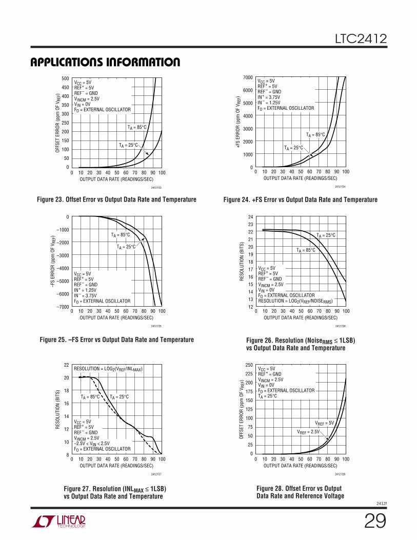
LTC2412
292412f
APPLICATIO S I FOR ATIO
WU UU
Figure 23. Offset Error vs Output Data Rate and Temperature Figure 24. +FS Error vs Output Data Rate and Temperature
Figure 25. –FS Error vs Output Data Rate and Temperature Figure 26. Resolution (NoiseRMS ≤ 1LSB)vs Output Data Rate and Temperature
Figure 27. Resolution (INLMAX ≤ 1LSB)vs Output Data Rate and Temperature
Figure 28. Offset Error vs OutputData Rate and Reference Voltage
OUTPUT DATA RATE (READINGS/SEC)0 10 20 30 40 50 60 70 80 90 100
OFFS
ET E
RROR
(ppm
OF
V REF
)
2412 F23
500
450
400
350
300
250
200
150
100
50
0
TA = 85°C
VCC = 5VREF+ = 5VREF – = GNDVINCM = 2.5VVIN = 0VFO = EXTERNAL OSCILLATOR
TA = 25°C
OUTPUT DATA RATE (READINGS/SEC)0 10 20 30 40 50 60 70 80 90 100
+FS
ERRO
R (p
pm O
F V R
EF)
2412 F24
7000
6000
5000
4000
3000
2000
1000
0
TA = 85°C
VCC = 5VREF+ = 5VREF – = GNDIN+ = 3.75VIN – = 1.25VFO = EXTERNAL OSCILLATOR
TA = 25°C
OUTPUT DATA RATE (READINGS/SEC)0 10 20 30 40 50 60 70 80 90 100
–FS
ERRO
R (p
pm O
F V R
EF)
2412 F25
0
–1000
–2000
–3000
–4000
–5000
–6000
–7000
TA = 85°C
VCC = 5VREF+ = 5VREF – = GNDIN+ = 1.25VIN – = 3.75VFO = EXTERNAL OSCILLATOR
TA = 25°C
OUTPUT DATA RATE (READINGS/SEC)0 10 20 30 40 50 60 70 80 90 100
RESO
LUTI
ON (B
ITS)
2412 F26
24
23
22
21
20
19
18
17
16
15
14
13
12
TA = 85°C
VCC = 5VREF+ = 5VREF – = GNDVINCM = 2.5VVIN = 0VFO = EXTERNAL OSCILLATORRESOLUTION = LOG2(VREF/NOISERMS)
TA = 25°C
OUTPUT DATA RATE (READINGS/SEC)0 10 20 30 40 50 60 70 80 90 100
RESO
LUTI
ON (B
ITS)
2412 F27
22
20
18
16
14
12
10
8
TA = 85°C
VCC = 5VREF+ = 5VREF – = GNDVINCM = 2.5V–2.5V < VIN < 2.5VFO = EXTERNAL OSCILLATOR
RESOLUTION = LOG2(VREF/INLMAX)
TA = 25°C
OUTPUT DATA RATE (READINGS/SEC)0 10 20 30 40 50 60 70 80 90 100
OFFS
ET E
RROR
(ppm
OF
V REF
)
2412 F28
250
225
200
175
150
125
100
75
50
25
0
VREF = 5V
VCC = 5VREF+ = GNDVINCM = 2.5VVIN = 0VFO = EXTERNAL OSCILLATORTA = 25°C
VREF = 2.5V
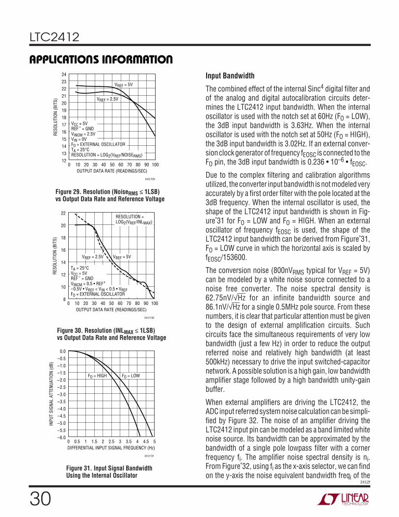
LTC2412
302412f
APPLICATIO S I FOR ATIO
WU UU
Input Bandwidth
The combined effect of the internal Sinc4 digital filter andof the analog and digital autocalibration circuits deter-mines the LTC2412 input bandwidth. When the internaloscillator is used with the notch set at 60Hz (FO = LOW),the 3dB input bandwidth is 3.63Hz. When the internaloscillator is used with the notch set at 50Hz (FO = HIGH),the 3dB input bandwidth is 3.02Hz. If an external conver-sion clock generator of frequency fEOSC is connected to theFO pin, the 3dB input bandwidth is 0.236 • 10–6 • fEOSC.
Due to the complex filtering and calibration algorithmsutilized, the converter input bandwidth is not modeled veryaccurately by a first order filter with the pole located at the3dB frequency. When the internal oscillator is used, theshape of the LTC2412 input bandwidth is shown in Fig-ure 31 for FO = LOW and FO = HIGH. When an externaloscillator of frequency fEOSC is used, the shape of theLTC2412 input bandwidth can be derived from Figure 31,FO = LOW curve in which the horizontal axis is scaled byfEOSC/153600.
The conversion noise (800nVRMS typical for VREF = 5V)can be modeled by a white noise source connected to anoise free converter. The noise spectral density is62.75nV/√Hz for an infinite bandwidth source and86.1nV/√Hz for a single 0.5MHz pole source. From thesenumbers, it is clear that particular attention must be givento the design of external amplification circuits. Suchcircuits face the simultaneous requirements of very lowbandwidth (just a few Hz) in order to reduce the outputreferred noise and relatively high bandwidth (at least500kHz) necessary to drive the input switched-capacitornetwork. A possible solution is a high gain, low bandwidthamplifier stage followed by a high bandwidth unity-gainbuffer.
When external amplifiers are driving the LTC2412, theADC input referred system noise calculation can be simpli-fied by Figure 32. The noise of an amplifier driving theLTC2412 input pin can be modeled as a band limited whitenoise source. Its bandwidth can be approximated by thebandwidth of a single pole lowpass filter with a cornerfrequency fi. The amplifier noise spectral density is ni.From Figure 32, using fi as the x-axis selector, we can findon the y-axis the noise equivalent bandwidth freqi of the
Figure 29. Resolution (NoiseRMS ≤ 1LSB)vs Output Data Rate and Reference Voltage
Figure 30. Resolution (INLMAX ≤ 1LSB)vs Output Data Rate and Reference Voltage
Figure 31. Input Signal BandwidthUsing the Internal Oscillator
OUTPUT DATA RATE (READINGS/SEC)0 10 20 30 40 50 60 70 80 90 100
RESO
LUTI
ON (B
ITS)
2412 F29
24
23
22
21
20
19
18
17
16
15
14
13
12
VREF = 5V
VCC = 5VREF – = GNDVINCM = 2.5VVIN = 0VFO = EXTERNAL OSCILLATORTA = 25°CRESOLUTION = LOG2(VREF/NOISERMS)
VREF = 2.5V
OUTPUT DATA RATE (READINGS/SEC)0 10 20 30 40 50 60 70 80 90 100
RESO
LUTI
ON (B
ITS)
2412 F30
22
20
18
16
14
12
10
8
TA = 25°CVCC = 5VREF – = GNDVINCM = 0.5 • REF+
–0.5V • VREF < VIN < 0.5 • VREFFO = EXTERNAL OSCILLATOR
VREF = 2.5V VREF = 5V
RESOLUTION = LOG2(VREF/INLMAX)
DIFFERENTIAL INPUT SIGNAL FREQUENCY (Hz)0 0.5 1 1.5 2 2.5 3 3.5 4 4.5 5
INPU
T SI
GNAL
ATT
ENUA
TION
(dB)
2412 F31
0.0
–0.5
–1.0
–1.5
–2.0
–2.5
–3.0
–3.5
–4.0
–4.5
–5.0
–5.5
–6.0
FO = HIGH FO = LOW
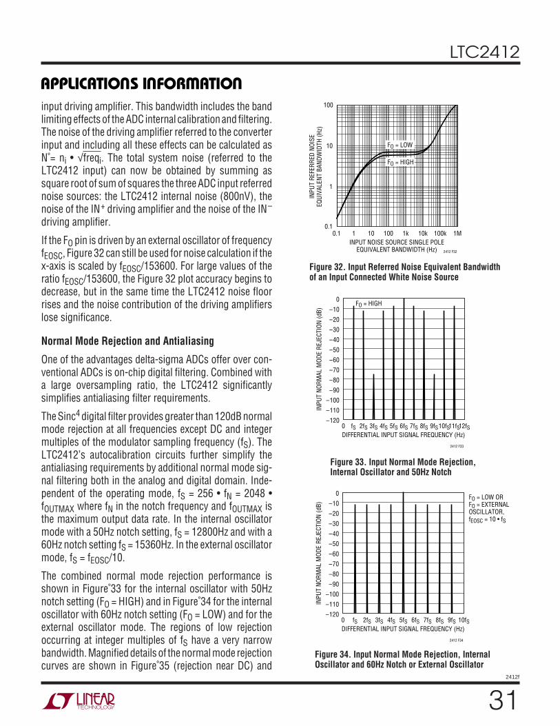
LTC2412
312412f
APPLICATIO S I FOR ATIO
WU UU
input driving amplifier. This bandwidth includes the bandlimiting effects of the ADC internal calibration and filtering.The noise of the driving amplifier referred to the converterinput and including all these effects can be calculated asN = ni • √freqi. The total system noise (referred to theLTC2412 input) can now be obtained by summing assquare root of sum of squares the three ADC input referrednoise sources: the LTC2412 internal noise (800nV), thenoise of the IN+ driving amplifier and the noise of the IN–
driving amplifier.
If the FO pin is driven by an external oscillator of frequencyfEOSC, Figure 32 can still be used for noise calculation if thex-axis is scaled by fEOSC/153600. For large values of theratio fEOSC/153600, the Figure 32 plot accuracy begins todecrease, but in the same time the LTC2412 noise floorrises and the noise contribution of the driving amplifierslose significance.
Normal Mode Rejection and Antialiasing
One of the advantages delta-sigma ADCs offer over con-ventional ADCs is on-chip digital filtering. Combined witha large oversampling ratio, the LTC2412 significantlysimplifies antialiasing filter requirements.
The Sinc4 digital filter provides greater than 120dB normalmode rejection at all frequencies except DC and integermultiples of the modulator sampling frequency (fS). TheLTC2412’s autocalibration circuits further simplify theantialiasing requirements by additional normal mode sig-nal filtering both in the analog and digital domain. Inde-pendent of the operating mode, fS = 256 • fN = 2048 •fOUTMAX where fN in the notch frequency and fOUTMAX isthe maximum output data rate. In the internal oscillatormode with a 50Hz notch setting, fS = 12800Hz and with a60Hz notch setting fS = 15360Hz. In the external oscillatormode, fS = fEOSC/10.
The combined normal mode rejection performance isshown in Figure 33 for the internal oscillator with 50Hznotch setting (FO = HIGH) and in Figure 34 for the internaloscillator with 60Hz notch setting (FO = LOW) and for theexternal oscillator mode. The regions of low rejectionoccurring at integer multiples of fS have a very narrowbandwidth. Magnified details of the normal mode rejectioncurves are shown in Figure 35 (rejection near DC) and
Figure 33. Input Normal Mode Rejection,Internal Oscillator and 50Hz Notch
Figure 34. Input Normal Mode Rejection, InternalOscillator and 60Hz Notch or External Oscillator
Figure 32. Input Referred Noise Equivalent Bandwidthof an Input Connected White Noise Source
INPUT NOISE SOURCE SINGLE POLEEQUIVALENT BANDWIDTH (Hz)
1
INPU
T RE
FERR
ED N
OISE
EQUI
VALE
NT B
ANDW
IDTH
(Hz)
10
0.1 1 10 100 1k 10k 100k 1M
2412 F32
0.1
100
FO = HIGH
FO = LOW
DIFFERENTIAL INPUT SIGNAL FREQUENCY (Hz)0 fS 2fS 3fS 4fS 5fS 6fS 7fS 8fS 9fS10fS11fS12fS
INPU
T NO
RMAL
MOD
E RE
JECT
ION
(dB)
2412 F33
0
–10
–20
–30
–40
–50
–60
–70
–80
–90
–100
–110
–120
FO = HIGH
FO = LOW OR FO = EXTERNALOSCILLATOR, fEOSC = 10 • fS
DIFFERENTIAL INPUT SIGNAL FREQUENCY (Hz)0 fS
INPU
T NO
RMAL
MOD
E RE
JECT
ION
(dB)
2412 F34
0
–10
–20
–30
–40
–50
–60
–70
–80
–90
–100
–110
–1202fS 3fS 4fS 5fS 6fS 7fS 8fS 9fS 10fS
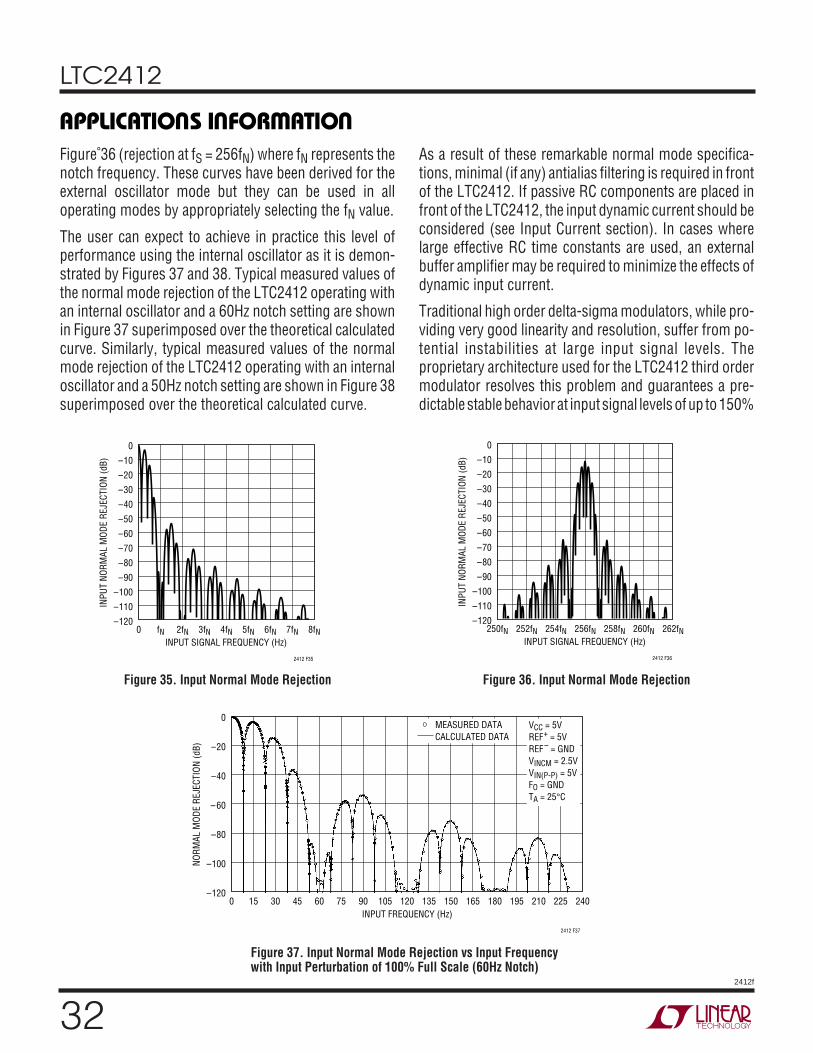
LTC2412
322412f
APPLICATIO S I FOR ATIO
WU UU
Figure 36 (rejection at fS = 256fN) where fN represents thenotch frequency. These curves have been derived for theexternal oscillator mode but they can be used in alloperating modes by appropriately selecting the fN value.
The user can expect to achieve in practice this level ofperformance using the internal oscillator as it is demon-strated by Figures 37 and 38. Typical measured values ofthe normal mode rejection of the LTC2412 operating withan internal oscillator and a 60Hz notch setting are shownin Figure 37 superimposed over the theoretical calculatedcurve. Similarly, typical measured values of the normalmode rejection of the LTC2412 operating with an internaloscillator and a 50Hz notch setting are shown in Figure 38superimposed over the theoretical calculated curve.
As a result of these remarkable normal mode specifica-tions, minimal (if any) antialias filtering is required in frontof the LTC2412. If passive RC components are placed infront of the LTC2412, the input dynamic current should beconsidered (see Input Current section). In cases wherelarge effective RC time constants are used, an externalbuffer amplifier may be required to minimize the effects ofdynamic input current.
Traditional high order delta-sigma modulators, while pro-viding very good linearity and resolution, suffer from po-tential instabilities at large input signal levels. Theproprietary architecture used for the LTC2412 third ordermodulator resolves this problem and guarantees a pre-dictable stable behavior at input signal levels of up to 150%
INPUT SIGNAL FREQUENCY (Hz)
INPU
T NO
RMAL
MOD
E RE
JECT
ION
(dB)
2412 F35
0
–10
–20
–30
–40
–50
–60
–70
–80
–90
–100
–110
–120fN0 2fN 3fN 4fN 5fN 6fN 7fN 8fN
INPUT SIGNAL FREQUENCY (Hz)250fN 252fN 254fN 256fN 258fN 260fN 262fN
INPU
T NO
RMAL
MOD
E RE
JECT
ION
(dB)
2412 F36
0
–10
–20
–30
–40
–50
–60
–70
–80
–90
–100
–110
–120
Figure 35. Input Normal Mode Rejection Figure 36. Input Normal Mode Rejection
Figure 37. Input Normal Mode Rejection vs Input Frequencywith Input Perturbation of 100% Full Scale (60Hz Notch)
INPUT FREQUENCY (Hz)0 15 30 45 60 75 90 105 120 135 150 165 180 195 210 225 240
NORM
AL M
ODE
REJE
CTIO
N (d
B)
2412 F37
0
–20
–40
–60
–80
–100
–120
VCC = 5VREF+ = 5VREF – = GNDVINCM = 2.5VVIN(P-P) = 5VFO = GNDTA = 25°C
MEASURED DATACALCULATED DATA
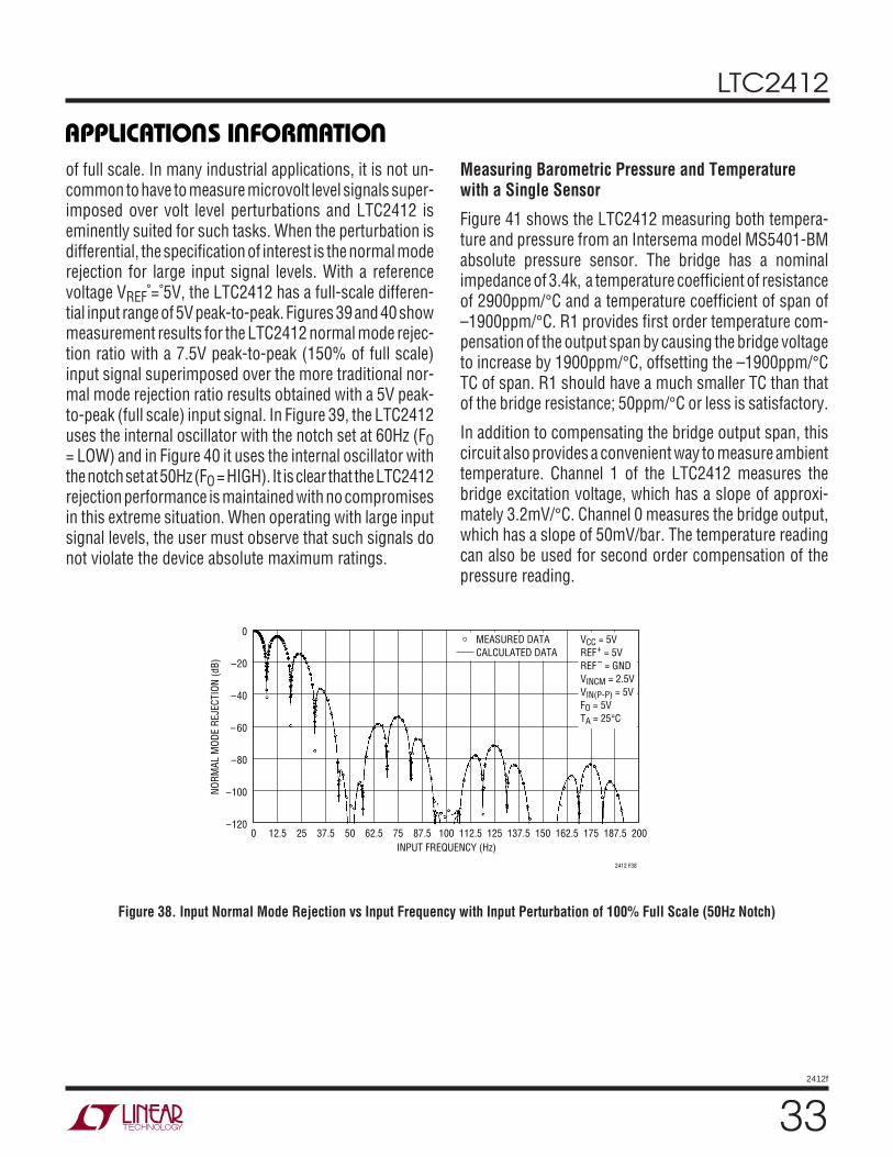
LTC2412
332412f
APPLICATIO S I FOR ATIO
WU UU
Figure 38. Input Normal Mode Rejection vs Input Frequency with Input Perturbation of 100% Full Scale (50Hz Notch)
of full scale. In many industrial applications, it is not un-common to have to measure microvolt level signals super-imposed over volt level perturbations and LTC2412 iseminently suited for such tasks. When the perturbation isdifferential, the specification of interest is the normal moderejection for large input signal levels. With a referencevoltage VREF = 5V, the LTC2412 has a full-scale differen-tial input range of 5V peak-to-peak. Figures 39 and 40 showmeasurement results for the LTC2412 normal mode rejec-tion ratio with a 7.5V peak-to-peak (150% of full scale)input signal superimposed over the more traditional nor-mal mode rejection ratio results obtained with a 5V peak-to-peak (full scale) input signal. In Figure 39, the LTC2412uses the internal oscillator with the notch set at 60Hz (FO= LOW) and in Figure 40 it uses the internal oscillator withthe notch set at 50Hz (FO = HIGH). It is clear that the LTC2412rejection performance is maintained with no compromisesin this extreme situation. When operating with large inputsignal levels, the user must observe that such signals donot violate the device absolute maximum ratings.
Measuring Barometric Pressure and Temperaturewith a Single Sensor
Figure 41 shows the LTC2412 measuring both tempera-ture and pressure from an Intersema model MS5401-BMabsolute pressure sensor. The bridge has a nominalimpedance of 3.4k, a temperature coefficient of resistanceof 2900ppm/°C and a temperature coefficient of span of–1900ppm/°C. R1 provides first order temperature com-pensation of the output span by causing the bridge voltageto increase by 1900ppm/°C, offsetting the –1900ppm/°CTC of span. R1 should have a much smaller TC than thatof the bridge resistance; 50ppm/°C or less is satisfactory.
In addition to compensating the bridge output span, thiscircuit also provides a convenient way to measure ambienttemperature. Channel 1 of the LTC2412 measures thebridge excitation voltage, which has a slope of approxi-mately 3.2mV/°C. Channel 0 measures the bridge output,which has a slope of 50mV/bar. The temperature readingcan also be used for second order compensation of thepressure reading.
INPUT FREQUENCY (Hz)0 12.5 25 37.5 50 62.5 75 87.5 100 112.5 125 137.5 150 162.5 175 187.5 200
NORM
AL M
ODE
REJE
CTIO
N (d
B)
2412 F38
0
–20
–40
–60
–80
–100
–120
VCC = 5VREF+ = 5VREF – = GNDVINCM = 2.5VVIN(P-P) = 5VFO = 5VTA = 25°C
MEASURED DATACALCULATED DATA
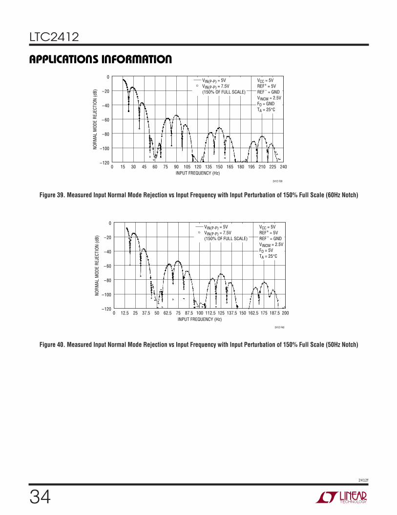
LTC2412
342412f
APPLICATIO S I FOR ATIO
WU UU
Figure 40. Measured Input Normal Mode Rejection vs Input Frequency with Input Perturbation of 150% Full Scale (50Hz Notch)
INPUT FREQUENCY (Hz)0
NORM
AL M
ODE
REJE
CTIO
N (d
B)
2412 F40
0
–20
–40
–60
–80
–100
–120
VCC = 5VREF+ = 5VREF – = GNDVINCM = 2.5VFO = 5VTA = 25°C
VIN(P-P) = 5VVIN(P-P) = 7.5V(150% OF FULL SCALE)
12.5 25 37.5 50 62.5 75 87.5 100 112.5 125 137.5 150 162.5 175 187.5 200
Figure 39. Measured Input Normal Mode Rejection vs Input Frequency with Input Perturbation of 150% Full Scale (60Hz Notch)
INPUT FREQUENCY (Hz)0 15 30 45 60 75 90 105 120 135 150 165 180 195 210 225 240
NORM
AL M
ODE
REJE
CTIO
N (d
B)
2412 F39
0
–20
–40
–60
–80
–100
–120
VCC = 5VREF+ = 5VREF – = GNDVINCM = 2.5VFO = GNDTA = 25°C
VIN(P-P) = 5VVIN(P-P) = 7.5V(150% OF FULL SCALE)
LTC2412
352412f
PACKAGE DESCRIPTIO
U
GN Package16-Lead Plastic SSOP (Narrow .150 Inch)
(Reference LTC DWG # 05-08-1641)
Information furnished by Linear Technology Corporation is believed to be accurate and reliable.However, no responsibility is assumed for its use. Linear Technology Corporation makes no represen-tation that the interconnection of its circuits as described herein will not infringe on existing patent rights.
GN16 (SSOP) 0502
1 2 3 4 5 6 7 8
.229 – .244(5.817 – 6.198)
.150 – .157**(3.810 – 3.988)
16 15 14 13
.189 – .196*(4.801 – 4.978)
12 11 10 9
.016 – .050(0.406 – 1.270)
.015 ± .004(0.38 ± 0.10)
× 45°
0° – 8° TYP.007 – .0098(0.178 – 0.249)
.053 – .068(1.351 – 1.727)
.008 – .012(0.203 – 0.305)
.004 – .0098(0.102 – 0.249)
.0250(0.635)
BSC
.009(0.229)
REF
.254 MIN
RECOMMENDED SOLDER PAD LAYOUT
.150 – .165
.0250 TYP.0165 ± .0015
.045 ±.005
*DIMENSION DOES NOT INCLUDE MOLD FLASH. MOLD FLASH SHALL NOT EXCEED 0.006" (0.152mm) PER SIDE**DIMENSION DOES NOT INCLUDE INTERLEAD FLASH. INTERLEAD FLASH SHALL NOT EXCEED 0.010" (0.254mm) PER SIDE
INCHES(MILLIMETERS)
NOTE:1. CONTROLLING DIMENSION: INCHES
2. DIMENSIONS ARE IN
3. DRAWING NOT TO SCALE
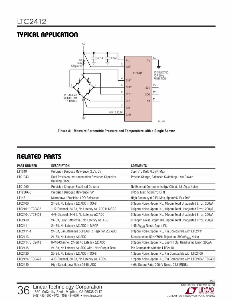
LTC2412
362412f
PART NUMBER DESCRIPTION COMMENTS
LT1019 Precision Bandgap Reference, 2.5V, 5V 3ppm/°C Drift, 0.05% Max
LTC1043 Dual Precision Instrumentation Switched Capacitor Precise Charge, Balanced Switching, Low PowerBuilding Block
LTC1050 Precision Chopper Stabilized Op Amp No External Components 5µV Offset, 1.6µVP-P Noise
LT1236A-5 Precision Bandgap Reference, 5V 0.05% Max, 5ppm/°C Drift
LT1461 Micropower Precision LDO Reference High Accuracy 0.04% Max, 3ppm/°C Max Drift
LTC2400 24-Bit, No Latency ∆Σ ADC in SO-8 0.3ppm Noise, 4ppm INL, 10ppm Total Unadjusted Error, 200µA
LTC2401/LTC2402 1-/2-Channel, 24-Bit, No Latency ∆Σ ADC in MSOP 0.6ppm Noise, 4ppm INL, 10ppm Total Unadjusted Error, 200µA
LTC2404/LTC2408 4-/8-Channel, 24-Bit, No Latency ∆Σ ADC 0.3ppm Noise, 4ppm INL, 10ppm Total Unadjusted Error, 200µA
LTC2410 24-Bit, Fully Differential, No Latency ∆Σ ADC 0.16ppm Noise, 2ppm INL, 3ppm Total Unadjusted Error, 200µA
LTC2411 24-Bit, No Latency ∆Σ ADC in MSOP 1.45µVRMS Noise, 2ppm INL
LTC2411-1 24-Bit, Simultaneous 50Hz/60Hz Rejection ∆Σ ADC 0.3ppm Noise, 2ppm INL, Pin Compatible with LTC2411
LTC2413 24-Bit, No Latency ∆Σ ADC Simultaneous 50Hz/60Hz Rejection, 800nVRMS Noise
LTC2414/LTC2418 8-/16-Channel, 24-Bit No Latency ∆Σ ADC 0.2ppm Noise, 2ppm INL, 3ppm Total Unadjusted Error, 200µA
LTC2415 24-Bit, No Latency ∆Σ ADC with 15Hz Output Rate Pin Compatible with the LTC2410
LTC2420 20-Bit, No Latency ∆Σ ADC in SO-8 1.2ppm Noise, 8ppm INL, Pin Compatible with LTC2400
LTC2424/LTC2428 4-/8-Channel, 20-Bit, No Latency ∆Σ ADCs 1.2ppm Noise, 8ppm INL, Pin Compatible with LTC2404/LTC2408
LTC2440 High Speed, Low Noise 24-Bit ADC 4kHz Output Rate, 200nV Noise, 24.6 ENOBs
Linear Technology Corporation1630 McCarthy Blvd., Milpitas, CA 95035-7417(408) 432-1900 FAX: (408) 434-0507 www.linear.com LINEAR TECHNOLOGY CORPORATION 2002
LT/TP 1202 2K • PRINTED IN USA
RELATED PARTS
0.1µF4.7µF 1
2
4
5
6
7
3
8,9,10,15,16
14
13
12
11
VCC
REF+
CH0+
CH0–
CH1+
CH1¯
REF–
GND
FO
SCK
SDO
CS
LTC2412 FO SELECTEDFOR 60HzREJECTION
INTERSEMAMSS401-BM
1 BAR FS
4
3
2
1
R16.8k
50ppm/°C
5V
2412 TA05
Figure 41. Measure Barometric Pressure and Temperature with a Single Sensor
TYPICAL APPLICATIO
U