SLAS541 -- JUNE 2007 D Low Supply-Voltage Range… · D Low Supply-Voltage Range: ... MSP430x2xx...
33
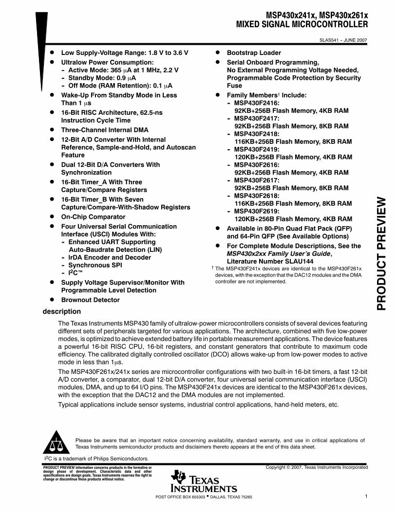
MSP430x241x, MSP430x261x MIXED SIGNAL MICROCONTROLLER SLAS541 -- JUNE 2007 1 POST OFFICE BOX 655303 • DALLAS, TEXAS 75265 D Low Supply-Voltage Range: 1.8 V to 3.6 V D Ultralow Power Consumption: -- Active Mode: 365 μA at 1 MHz, 2.2 V -- Standby Mode: 0.9 μA -- Off Mode (RAMRetention): 0.1 μA D Wake-Up From Standby Mode in Less Than 1 μs D 16-Bit RISC Architecture, 62.5-ns Instruction Cycle Time D Three-Channel Internal DMA D 12-Bit A/D Converter With Internal Reference, Sample-and-Hold, and Autoscan Feature D Dual 12-Bit D/A Converters With Synchronization D 16-Bit Timer_A With Three Capture/Compare Registers D 16-Bit Timer_B With Seven Capture/Compare-With-Shadow Registers D On-Chip Comparator D Four Universal Serial Communication Interface (USCI) Modules With: -- Enhanced UART Supporting Auto-Baudrate Detection (LIN) -- IrDA Encoder and Decoder -- Synchronous SPI -- I 2 C™ D Supply Voltage Supervisor/Monitor With Programmable Level Detection D Brownout Detector D Bootstrap Loader D Serial Onboard Programming, No External Programming Voltage Needed, Programmable Code Protection by Security Fuse D Family Members † Include: -- MSP430F2416: 92KB+256B Flash Memory, 4KB RAM -- MSP430F2417: 92KB+256B Flash Memory, 8KB RAM -- MSP430F2418: 116KB+256B Flash Memory, 8KB RAM -- MSP430F2419: 120KB+256B Flash Memory, 4KB RAM -- MSP430F2616: 92KB+256B Flash Memory, 4KB RAM -- MSP430F2617: 92KB+256B Flash Memory, 8KB RAM -- MSP430F2618: 116KB+256B Flash Memory, 8KB RAM -- MSP430F2619: 120KB+256B Flash Memory, 4KB RAM D Available in 80-Pin Quad Flat Pack (QFP) and 64-Pin QFP (See Available Options) D For Complete Module Descriptions, See the MSP430x2xx Family User’s Guide, Literature Number SLAU144 † The MSP430F241x devices are identical to the MSP430F261x devices, with the exception that the DAC12 modules and the DMA controller are not implemented. description The Texas Instruments MSP430 family of ultralow-power microcontrollers consists of several devices featuring different sets of peripherals targeted for various applications. The architecture, combined with five low-power modes, is optimized to achieve extended battery life in portable measurement applications. The device features a powerful 16-bit RISC CPU, 16-bit registers, and constant generators that contribute to maximum code efficiency. The calibrated digitally controlled oscillator (DCO) allows wake-up from low-power modes to active mode in less than 1μs. The MSP430F261x/241x series are microcontroller configurations with two built-in 16-bit timers, a fast 12-bit A/D converter, a comparator, dual 12-bit D/A converter, four universal serial communication interface (USCI) modules, DMA, and up to 64 I/O pins. The MSP430F241x devices are identical to the MSP430F261x devices, with the exception that the DAC12 and the DMA modules are not implemented. Typical applications include sensor systems, industrial control applications, hand-held meters, etc. PRODUCT PREVIEW Copyright © 2007, Texas Instruments Incorporated Please be aware that an important notice concerning availability, standard warranty, and use in critical applications of Texas Instruments semiconductor products and disclaimers thereto appears at the end of this data sheet. I 2 C is a trademark of Philips Semiconductors. PRODUCT PREVIEW information concerns products in the formative or design phase of development. Characteristic data and other specifications are design goals. Texas Instruments reserves the right to change or discontinue these products without notice.
Transcript of SLAS541 -- JUNE 2007 D Low Supply-Voltage Range… · D Low Supply-Voltage Range: ... MSP430x2xx...
MSP430x241x, MSP430x261xMIXED SIGNAL MICROCONTROLLER
SLAS541 -- JUNE 2007
1POST OFFICE BOX 655303 • DALLAS, TEXAS 75265
D Low Supply-Voltage Range: 1.8 V to 3.6 VD Ultralow Power Consumption:
-- Active Mode: 365 μA at 1 MHz, 2.2 V-- Standby Mode: 0.9 μA-- Off Mode (RAM Retention): 0.1 μA
D Wake-Up From Standby Mode in LessThan 1 μs
D 16-Bit RISC Architecture, 62.5-nsInstruction Cycle Time
D Three-Channel Internal DMAD 12-Bit A/D Converter With Internal
Reference, Sample-and-Hold, and AutoscanFeature
D Dual 12-Bit D/A Converters WithSynchronization
D 16-Bit Timer_A With ThreeCapture/Compare Registers
D 16-Bit Timer_B With SevenCapture/Compare-With-Shadow Registers
D On-Chip ComparatorD Four Universal Serial Communication
Interface (USCI) Modules With:-- Enhanced UART SupportingAuto-Baudrate Detection (LIN)
-- IrDA Encoder and Decoder-- Synchronous SPI-- I2C™
D Supply Voltage Supervisor/Monitor WithProgrammable Level Detection
D Brownout Detector
D Bootstrap LoaderD Serial Onboard Programming,
No External Programming Voltage Needed,Programmable Code Protection by SecurityFuse
D Family Members† Include:-- MSP430F2416:92KB+256B Flash Memory, 4KB RAM
-- MSP430F2417:92KB+256B Flash Memory, 8KB RAM
-- MSP430F2418:116KB+256B Flash Memory, 8KB RAM
-- MSP430F2419:120KB+256B Flash Memory, 4KB RAM
-- MSP430F2616:92KB+256B Flash Memory, 4KB RAM
-- MSP430F2617:92KB+256B Flash Memory, 8KB RAM
-- MSP430F2618:116KB+256B Flash Memory, 8KB RAM
-- MSP430F2619:120KB+256B Flash Memory, 4KB RAM
D Available in 80-Pin Quad Flat Pack (QFP)and 64-Pin QFP (See Available Options)
D For Complete Module Descriptions, See theMSP430x2xx Family User’s Guide,Literature Number SLAU144
† The MSP430F241x devices are identical to the MSP430F261xdevices, with the exception that theDAC12modules and theDMAcontroller are not implemented.
description
The Texas InstrumentsMSP430 family of ultralow-powermicrocontrollers consists of several devices featuringdifferent sets of peripherals targeted for various applications. The architecture, combined with five low-powermodes, is optimized to achieve extendedbattery life in portablemeasurement applications. The device featuresa powerful 16-bit RISC CPU, 16-bit registers, and constant generators that contribute to maximum codeefficiency. The calibrated digitally controlled oscillator (DCO) allows wake-up from low-power modes to activemode in less than 1μs.The MSP430F261x/241x series are microcontroller configurations with two built-in 16-bit timers, a fast 12-bitA/D converter, a comparator, dual 12-bit D/A converter, four universal serial communication interface (USCI)modules, DMA, and up to 64 I/O pins. The MSP430F241x devices are identical to the MSP430F261x devices,with the exception that the DAC12 and the DMA modules are not implemented.Typical applications include sensor systems, industrial control applications, hand-held meters, etc.
PRODUCTPREVIEW
Copyright © 2007, Texas Instruments Incorporated
Please be aware that an important notice concerning availability, standard warranty, and use in critical applications ofTexas Instruments semiconductor products and disclaimers thereto appears at the end of this data sheet.
I2C is a trademark of Philips Semiconductors.
PRODUCT PREVIEW information concerns products in the formative ordesign phase of development. Characteristic data and otherspecifications are design goals. Texas Instruments reserves the right tochange or discontinue these products without notice.
MSP430x241x, MSP430x261xMIXED SIGNAL MICROCONTROLLER
SLAS541 -- JUNE 2007
2 POST OFFICE BOX 655303 • DALLAS, TEXAS 75265
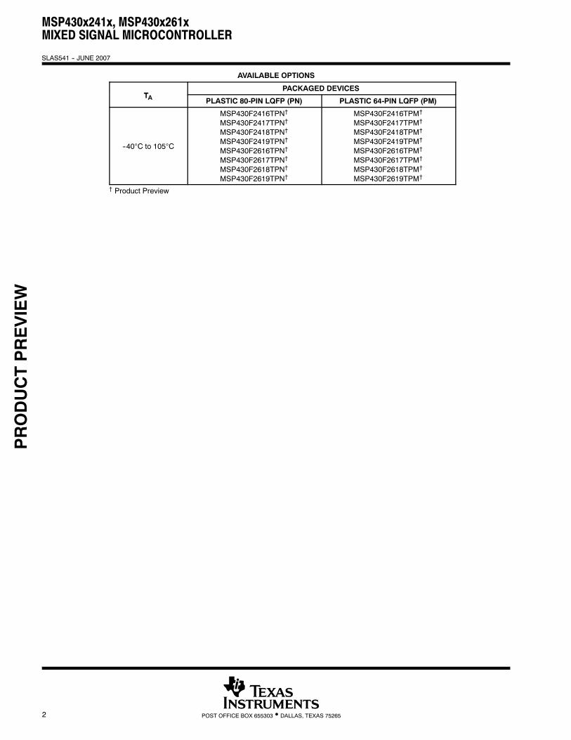
AVAILABLE OPTIONS
TPACKAGED DEVICES
TA PLASTIC 80-PIN LQFP (PN) PLASTIC 64-PIN LQFP (PM)
--40°C to 105°C
MSP430F2416TPN†
MSP430F2417TPN†
MSP430F2418TPN†
MSP430F2419TPN†
MSP430F2616TPN†
MSP430F2617TPN†
MSP430F2618TPN†
MSP430F2619TPN†
MSP430F2416TPM†
MSP430F2417TPM†
MSP430F2418TPM†
MSP430F2419TPM†
MSP430F2616TPM†
MSP430F2617TPM†
MSP430F2618TPM†
MSP430F2619TPM†
† Product Preview
PRODUCTPREVIEW
MSP430x241x, MSP430x261xMIXED SIGNAL MICROCONTROLLER
SLAS541 -- JUNE 2007
3POST OFFICE BOX 655303 • DALLAS, TEXAS 75265
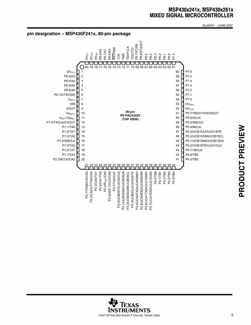
pin designation -- MSP430F241x, 80-pin package
80-pinPN PACKAGE
(TOP VIEW)
DVCC1 6059
80 79
P6.3/A3P6.4/A4P6.5/A5P6.6/A6
P6.7/A7/SVSINVREF+
XINXOUTVeREF+
VREF-/VeREF-
P1.0/TACLK/CAOUTP1.1/TA0P1.2/TA1P1.3/TA2
P1.4/SMCLK
P2.
1/TA
INC
LK/C
A3P2
.2/C
AOU
T/TA
0/C
A4P
2.3/
CA0
/TA1
P2.
4/C
A1/T
A2P2
.5/R
OSC
/CA5
P2.
7/TA
0/C
A7P3
.0/U
CB0
STE/
UC
A0C
LKP3
.1/U
CB
0SIM
O/U
CB
0SD
AP
3.2/
UC
B0S
OM
I/UC
B0S
CL
P3.3
/UC
B0C
LK/U
CA
0STE
P3.
4/U
CA0
TXD
/UC
A0S
IMO
P4.5/TB5P4.6/TB6P4.7/TBCLK
P5.4/MCLK
AV C
C
DV S
S1
AVS
S
P6.2
/A2
P6.1
/A1
P6.0
/A0
RS
T/N
MI
TCK
TMS
TDI/T
CLK
TDO
/TD
I
P5.5/SMCLK
78 77 76 75 74 73 72 71 70 69 68 67 66 65
5857565554535251504948474645
12345678910111213141516
21 22 23 24 25 26 27 28 29 30 31 32 33 34 35 36
64 63 62 61
37
P3.5
/UC
A0R
XD
/UC
A0S
OM
I
38 39 40
44434241
P1.5/TA0P1.6/TA1P1.7/TA2
P2.0/ACLK/CA2
17181920
P4.0
/TB0
P4.
1/TB
1P
4.2/
TB2
P4.
3/TB
3P
4.4/
TB4
P3.
6/U
CA1
TXD
/UC
A1S
IMO
P3.7
/UC
A1R
XD
/UC
A1S
OM
IP5.0/UCB1STE/UCA1CLKP5.1/UCB1SIMO/UCB1SDAP5.2/UCB1SOMI/UCB1SCLP5.3/UCB1CLK/UCA1STE
P7.0P7.1P7.2P7.3P7.4P7.5P7.6
P7.7
P8.0
P8.1
P8.2
P8.3
P8.4
P8.5
DVCC2
DVSS2
P5.7/TBOUTH/SVSOUTP5.6/ACLK
P8.6
/XT2
OU
TP8
.7/X
T2IN
P2.
6/A
DC
12C
LK/C
A6
PRODUCTPREVIEW
MSP430x241x, MSP430x261xMIXED SIGNAL MICROCONTROLLER
SLAS541 -- JUNE 2007
4 POST OFFICE BOX 655303 • DALLAS, TEXAS 75265
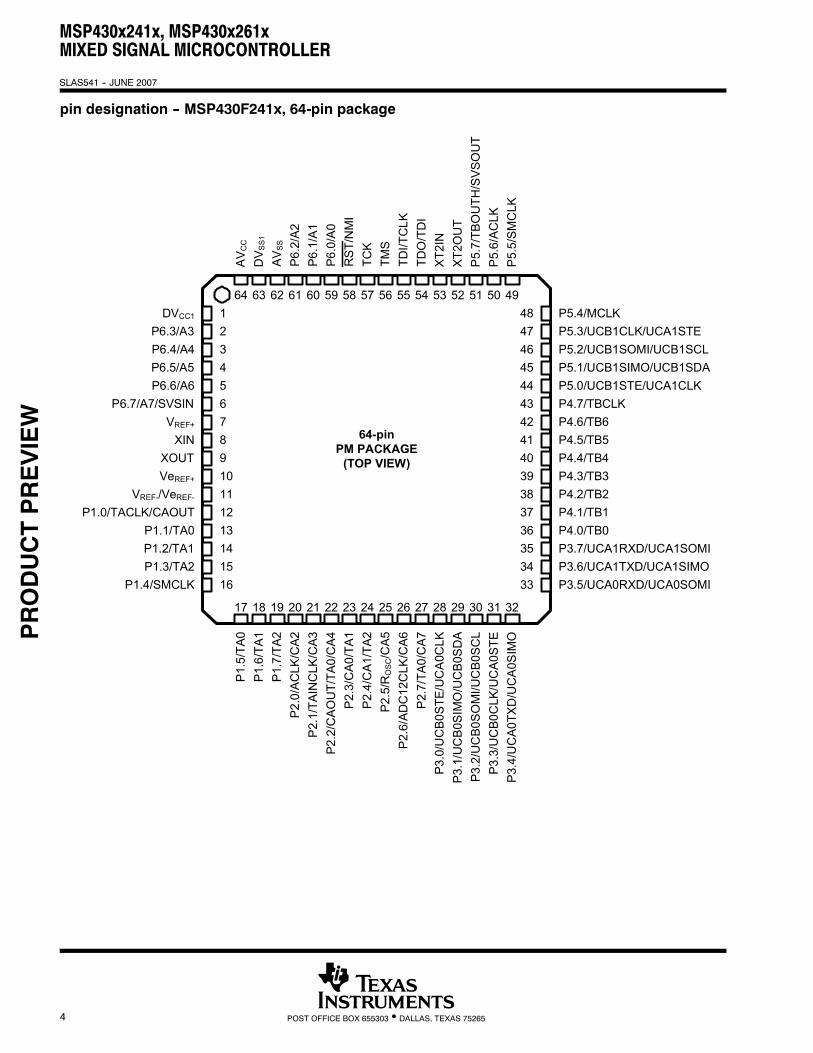
pin designation -- MSP430F241x, 64-pin package
DVCC1 4847
64 63
P6.3/A3P6.4/A4P6.5/A5
VREF+
XINXOUTVeREF+
VREF-/VeREF-
P1.0/TACLK/CAOUTP1.1/TA0P1.2/TA1P1.3/TA2
P1.4/SMCLK
P1.
5/TA
0P
1.6/
TA1
P1.
7/TA
2P2
.0/A
CLK
/CA2
P2.
1/TA
INC
LK/C
A3P2
.2/C
AO
UT/
TA0/
CA4
P2.
3/C
A0/T
A1P
2.4/
CA1
/TA2
P2.5
/RO
SC/C
A5P
2.6/
AD
C12
CLK
/CA6
P2.
7/TA
0/C
A7
P4.0/TB0P4.1/TB1P4.2/TB2P4.3/TB3P4.4/TB4P4.5/TB5P4.6/TB6P4.7/TBCLK
AV C
C
DV S
S1
AVS
S
P6.2
/A2
P6.1
/A1
P6.0
/A0
RS
T/N
MI
TCK
TMS
TDI/T
CLK
TDO
/TD
IX
T2IN
XT2
OU
T
62 61 60 59 58 57 56 55 54 53 52 51 50 49
4645444342414039383736353433
12345678910111213141516
17 18 19 20 21 22 23 24 25 26 27 28 29 30 31 32
P3.6/UCA1TXD/UCA1SIMOP3.7/UCA1RXD/UCA1SOMI
P5.0/UCB1STE/UCA1CLKP5.1/UCB1SIMO/UCB1SDAP5.2/UCB1SOMI/UCB1SCL
P5.4/MCLK
P5.
5/SM
CLK
P5.3/UCB1CLK/UCA1STE
P5.
7/TB
OU
TH/S
VSO
UT
P5.
6/AC
LK
P6.6/A6P6.7/A7/SVSIN
64-pinPM PACKAGE
(TOP VIEW)
P3.0
/UC
B0ST
E/U
CA
0CLK
P3.1
/UC
B0S
IMO
/UC
B0S
DA
P3.2
/UC
B0S
OM
I/UC
B0S
CL
P3.3
/UC
B0C
LK/U
CA
0STE
P3.
4/U
CA0
TXD
/UC
A0S
IMO
P3.5/UCA0RXD/UCA0SOMI
PRODUCTPREVIEW
MSP430x241x, MSP430x261xMIXED SIGNAL MICROCONTROLLER
SLAS541 -- JUNE 2007
5POST OFFICE BOX 655303 • DALLAS, TEXAS 75265
pin designation -- MSP430F261x, 80-pin package
80-pinPN PACKAGE
(TOP VIEW)
DVCC1 6059
80 79
P6.3/A3P6.4/A4
P6.5/A5/DAC1P6.6/A6/DAC0
P6.7/A7/DAC1/SVSINVREF+
XINXOUT
VeREF+/DAC0VREF-/VeREF-
P1.0/TACLK/CAOUTP1.1/TA0P1.2/TA1P1.3/TA2
P1.4/SMCLK
P2.
1/TA
INC
LK/C
A3P2
.2/C
AOU
T/TA
0/C
A4P
2.3/
CA0
/TA1
P2.
4/C
A1/T
A2P
2.5/
RO
SC/C
A5
P2.
7/TA
0/C
A7P
3.0/
UC
B0ST
E/U
CA
0CLK
P3.1
/UC
B0S
IMO
/UC
B0S
DA
P3.2
/UC
B0SO
MI/U
CB
0SC
LP
3.3/
UC
B0C
LK/U
CA
0STE
P3.
4/U
CA0
TXD
/UC
A0S
IMO
P4.5/TB5P4.6/TB6P4.7/TBCLK
P5.4/MCLK
AV C
C
DV S
S1
AVS
S
P6.2
/A2
P6.1
/A1
P6.0
/A0
RS
T/N
MI
TCK
TMS
TDI/T
CLK
TDO
/TD
I
P5.5/SMCLK
78 77 76 75 74 73 72 71 70 69 68 67 66 65
5857565554535251504948474645
12345678910111213141516
21 22 23 24 25 26 27 28 29 30 31 32 33 34 35 36
64 63 62 61
37
P3.5
/UC
A0R
XD
/UC
A0S
OM
I
38 39 40
44434241
P1.5/TA0P1.6/TA1P1.7/TA2
P2.0/ACLK/CA2
17181920
P4.0
/TB0
P4.
1/TB
1P
4.2/
TB2
P4.
3/TB
3P
4.4/
TB4
P3.
6/U
CA1
TXD
/UC
A1S
IMO
P3.7
/UC
A1R
XD
/UC
A1S
OM
IP5.0/UCB1STE/UCA1CLKP5.1/UCB1SIMO/UCB1SDAP5.2/UCB1SOMI/UCB1SCLP5.3/UCB1CLK/UCA1STE
P7.0P7.1P7.2P7.3P7.4P7.5P7.6
P7.7
P8.0
P8.1
P8.2
P8.3
P8.4
P8.5
DVCC2
DVSS2
P5.7/TBOUTH/SVSOUTP5.6/ACLK
P8.6
/XT2
OU
TP8
.7/X
T2IN
P2.6
/AD
C12
CLK
/DM
AE0/
CA6
PRODUCTPREVIEW
MSP430x241x, MSP430x261xMIXED SIGNAL MICROCONTROLLER
SLAS541 -- JUNE 2007
6 POST OFFICE BOX 655303 • DALLAS, TEXAS 75265
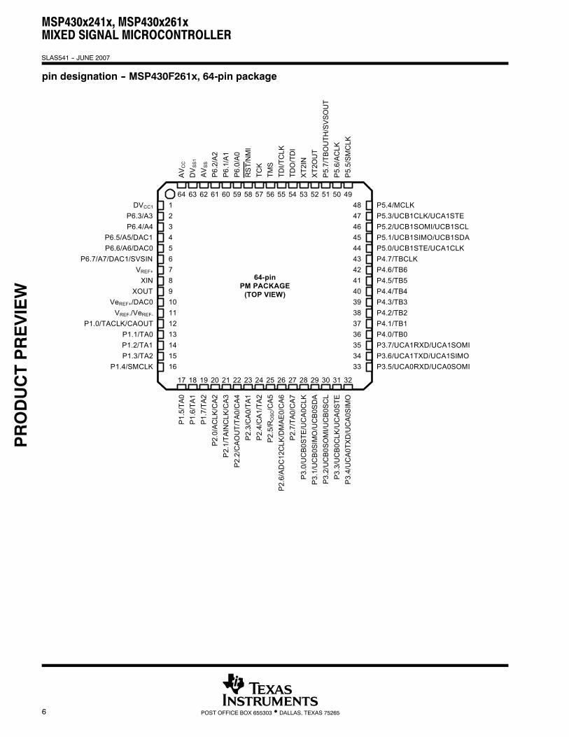
pin designation -- MSP430F261x, 64-pin package
DVCC1 4847
64 63
P6.3/A3P6.4/A4
P6.5/A5/DAC1
VREF+
XINXOUT
VeREF+/DAC0VREF-/VeREF-
P1.0/TACLK/CAOUTP1.1/TA0P1.2/TA1P1.3/TA2
P1.4/SMCLK
P1.
5/TA
0P
1.6/
TA1
P1.
7/TA
2P2
.0/A
CLK
/CA2
P2.
1/TA
INC
LK/C
A3P2
.2/C
AOU
T/TA
0/C
A4P
2.3/
CA
0/TA
1P
2.4/
CA
1/TA
2P2
.5/R
OSC
/CA5
P2.6
/AD
C12
CLK
/DM
AE0/
CA6
P2.
7/TA
0/C
A7P3
.0/U
CB0
STE
/UC
A0C
LKP3
.1/U
CB
0SIM
O/U
CB
0SD
AP3
.2/U
CB0
SOM
I/UC
B0S
CL
P3.3
/UC
B0C
LK/U
CA
0STE
P3.
4/U
CA0
TXD
/UC
A0S
IMO
P3.5/UCA0RXD/UCA0SOMI
P4.0/TB0P4.1/TB1P4.2/TB2P4.3/TB3P4.4/TB4P4.5/TB5P4.6/TB6P4.7/TBCLK
AV C
C
DV
SS
1
AVS
S
P6.2
/A2
P6.1
/A1
P6.0
/A0
RS
T/N
MI
TCK
TMS
TDI/T
CLK
TDO
/TD
IX
T2IN
XT2
OU
T
62 61 60 59 58 57 56 55 54 53 52 51 50 49
4645444342414039383736353433
12345678910111213141516
17 18 19 20 21 22 23 24 25 26 27 28 29 30 31 32
P3.6/UCA1TXD/UCA1SIMOP3.7/UCA1RXD/UCA1SOMI
P5.0/UCB1STE/UCA1CLKP5.1/UCB1SIMO/UCB1SDAP5.2/UCB1SOMI/UCB1SCL
P5.4/MCLK
P5.
5/SM
CLK
P5.3/UCB1CLK/UCA1STE
P5.
7/TB
OU
TH/S
VSO
UT
P5.
6/AC
LK
P6.6/A6/DAC0P6.7/A7/DAC1/SVSIN
64-pinPM PACKAGE
(TOP VIEW)
PRODUCTPREVIEW
MSP430x241x, MSP430x261xMIXED SIGNAL MICROCONTROLLER
SLAS541 -- JUNE 2007
7POST OFFICE BOX 655303 • DALLAS, TEXAS 75265
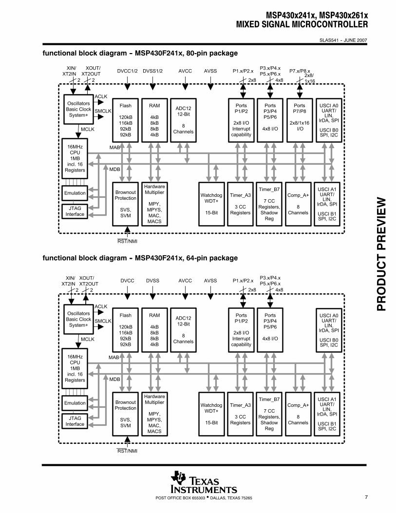
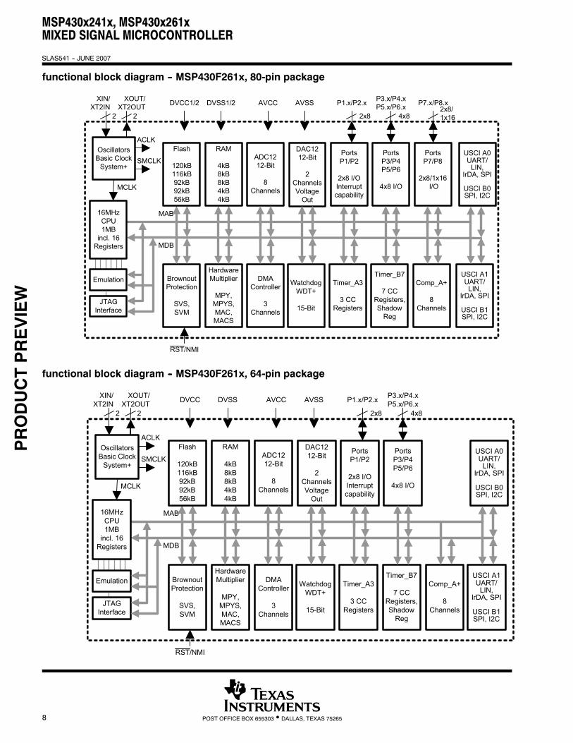
functional block diagram -- MSP430F241x, 80-pin package
OscillatorsBasic Clock
System+
Brownout Protection
SVS,SVM
RST/NMI
DVCC1/2 DVSS1/2
MCLK
WatchdogWDT+
15-Bit
Timer_A3
3 CC Registers
16MHzCPU1MB
incl. 16 Registers
Emulation
JTAGInterface
Ports P1/P2
2x8 I/O Interrupt capability
USCI A1UART/
LIN,IrDA, SPI
USCI B1SPI, I2C
Comp_A+
8 Channels
Hardware Multiplier
MPY, MPYS, MAC, MACS
Timer_B7
7 CC Registers, Shadow
Reg
ADC1212-Bit
8Channels
PortsP3/P4P5/P6
4x8 I/O
AVCC AVSS P1.x/P2.x
2x8
P3.x/P4.xP5.x/P6.x
4x8
SMCLK
ACLK
MDB
MAB
XIN/XT2IN
22
XOUT/XT2OUT
RAM
4kB8kB8kB4kB
Flash
120kB116kB92kB92kB
PortsP7/P8
2x8/1x16 I/O
P7.x/P8.x2x8/1x16
USCI A0UART/
LIN,IrDA, SPI
USCI B0SPI, I2C
functional block diagram -- MSP430F241x, 64-pin package
OscillatorsBasic Clock
System+
RAM
4kB8kB8kB4kB
Brownout Protection
SVS, SVM
RST/NMI
DVCC DVSS
MCLK
WatchdogWDT+
15-Bit
Timer_A3
3 CC Registers
16MHzCPU1MB
incl. 16 Registers
Emulation
XOUT/XT2OUT
JTAGInterface
Ports P1/P2
2x8 I/O Interrupt capability
Comp_A+
8 Channels
Flash
120kB116kB92kB92kB
Hardware Multiplier
MPY, MPYS, MAC, MACS
Timer_B7
7 CC Registers, Shadow
Reg
ADC1212-Bit
8Channels
PortsP3/P4P5/P6
4x8 I/O
AVCC AVSS P1.x/P2.x
2x8
P3.x/P4.xP5.x/P6.x
4x8
SMCLK
ACLK
MDB
MAB
XIN/XT2IN
22
USCI A1UART/
LIN,IrDA, SPI
USCI B1SPI, I2C
USCI A0UART/
LIN,IrDA, SPI
USCI B0SPI, I2C
PRODUCTPREVIEW
MSP430x241x, MSP430x261xMIXED SIGNAL MICROCONTROLLER
SLAS541 -- JUNE 2007
8 POST OFFICE BOX 655303 • DALLAS, TEXAS 75265
functional block diagram -- MSP430F261x, 80-pin package
OscillatorsBasic Clock
System+
Brownout Protection
SVS,SVM
RST/NMI
DVCC1/2 DVSS1/2
MCLK
WatchdogWDT+
15-Bit
Timer_A3
3 CC Registers
16MHzCPU1MB
incl. 16 Registers
Emulation
JTAGInterface
Ports P1/P2
2x8 I/O Interrupt capability
Comp_A+
8 Channels
Hardware Multiplier
MPY, MPYS, MAC, MACS
Timer_B7
7 CC Registers, Shadow
Reg
ADC1212-Bit
8Channels
PortsP3/P4P5/P6
4x8 I/O
AVCC AVSS P1.x/P2.x
2x8
P3.x/P4.xP5.x/P6.x
4x8
SMCLK
ACLK
MDB
MAB
DAC1212-Bit
2ChannelsVoltage
Out
PortsP7/P8
2x8/1x16 I/O
P7.x/P8.x2x8/1x16
DMA Controller
3 Channels
XIN/XT2IN
22
XOUT/XT2OUT
RAM
4kB8kB8kB4kB4kB
Flash
120kB116kB92kB92kB56kB
USCI A1UART/
LIN,IrDA, SPI
USCI B1SPI, I2C
USCI A0UART/
LIN,IrDA, SPI
USCI B0SPI, I2C
functional block diagram -- MSP430F261x, 64-pin package
USCI A0UART/
LIN,IrDA, SPI
USCI B0SPI, I2C
OscillatorsBasic Clock
System+
Brownout Protection
SVS,SVM
RST/NMI
DVCC DVSS
MCLK
WatchdogWDT+
15-Bit
Timer_A3
3 CC Registers
16MHzCPU1MB
incl. 16 Registers
Emulation
JTAGInterface
Ports P1/P2
2x8 I/O Interrupt capability
Comp_A+
8 Channels
Hardware Multiplier
MPY, MPYS, MAC, MACS
Timer_B7
7 CC Registers, Shadow
Reg
ADC1212-Bit
8Channels
PortsP3/P4P5/P6
4x8 I/O
AVCC AVSS P1.x/P2.x
2x8
P3.x/P4.xP5.x/P6.x
4x8
SMCLK
ACLK
MDB
MAB
DAC1212-Bit
2ChannelsVoltage
Out
DMA Controller
3 Channels
XIN/XT2IN
22
XOUT/XT2OUT
RAM
4kB8kB8kB4kB4kB
Flash
120kB116kB92kB92kB56kB
USCI A1UART/
LIN,IrDA, SPI
USCI B1SPI, I2C
PRODUCTPREVIEW
MSP430x241x, MSP430x261xMIXED SIGNAL MICROCONTROLLER
SLAS541 -- JUNE 2007
9POST OFFICE BOX 655303 • DALLAS, TEXAS 75265
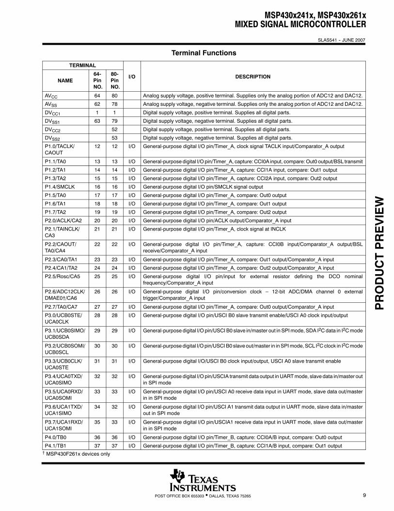
Terminal Functions
TERMINAL
NAME64-PinNO.
80-PinNO.
I/O DESCRIPTION
AVCC 64 80 Analog supply voltage, positive terminal. Supplies only the analog portion of ADC12 and DAC12.
AVSS 62 78 Analog supply voltage, negative terminal. Supplies only the analog portion of ADC12 and DAC12.
DVCC1 1 1 Digital supply voltage, positive terminal. Supplies all digital parts.
DVSS1 63 79 Digital supply voltage, negative terminal. Supplies all digital parts.
DVCC2 52 Digital supply voltage, positive terminal. Supplies all digital parts.
DVSS2 53 Digital supply voltage, negative terminal. Supplies all digital parts.
P1.0/TACLK/CAOUT
12 12 I/O General-purpose digital I/O pin/Timer_A, clock signal TACLK input/Comparator_A output
P1.1/TA0 13 13 I/O General-purpose digital I/O pin/Timer_A, capture: CCI0A input, compare:Out0 output/BSL transmit
P1.2/TA1 14 14 I/O General-purpose digital I/O pin/Timer_A, capture: CCI1A input, compare: Out1 output
P1.3/TA2 15 15 I/O General-purpose digital I/O pin/Timer_A, capture: CCI2A input, compare: Out2 output
P1.4/SMCLK 16 16 I/O General-purpose digital I/O pin/SMCLK signal output
P1.5/TA0 17 17 I/O General-purpose digital I/O pin/Timer_A, compare: Out0 output
P1.6/TA1 18 18 I/O General-purpose digital I/O pin/Timer_A, compare: Out1 output
P1.7/TA2 19 19 I/O General-purpose digital I/O pin/Timer_A, compare: Out2 output
P2.0/ACLK/CA2 20 20 I/O General-purpose digital I/O pin/ACLK output/Comparator_A input
P2.1/TAINCLK/CA3
21 21 I/O General-purpose digital I/O pin/Timer_A, clock signal at INCLK
P2.2/CAOUT/TA0/CA4
22 22 I/O General-purpose digital I/O pin/Timer_A, capture: CCI0B input/Comparator_A output/BSLreceive/Comparator_A input
P2.3/CA0/TA1 23 23 I/O General-purpose digital I/O pin/Timer_A, compare: Out1 output/Comparator_A input
P2.4/CA1/TA2 24 24 I/O General-purpose digital I/O pin/Timer_A, compare: Out2 output/Comparator_A input
P2.5/Rosc/CA5 25 25 I/O General-purpose digital I/O pin/input for external resistor defining the DCO nominalfrequency/Comparator_A input
P2.6/ADC12CLK/DMAE0†/CA6
26 26 I/O General-purpose digital I/O pin/conversion clock – 12-bit ADC/DMA channel 0 externaltrigger/Comparator_A input
P2.7/TA0/CA7 27 27 I/O General-purpose digital I/O pin/Timer_A, compare: Out0 output/Comparator_A input
P3.0/UCB0STE/UCA0CLK
28 28 I/O General-purpose digital I/O pin/USCI B0 slave transmit enable/USCI A0 clock input/output
P3.1/UCB0SIMO/UCB0SDA
29 29 I/O General-purpose digital I/O pin/USCI B0 slave in/master out in SPImode, SDA I2C data in I2Cmode
P3.2/UCB0SOMI/UCB0SCL
30 30 I/O General-purposedigital I/Opin/USCIB0slaveout/master in inSPImode, SCL I2C clock in I2Cmode
P3.3/UCB0CLK/UCA0STE
31 31 I/O General-purpose digital I/O/USCI B0 clock input/output, USCI A0 slave transmit enable
P3.4/UCA0TXD/UCA0SIMO
32 32 I/O General-purpose digital I/Opin/USCIA transmit data output inUARTmode, slave data in/master outin SPI mode
P3.5/UCA0RXD/UCA0SOMI
33 33 I/O General-purpose digital I/O pin/USCI A0 receive data input in UART mode, slave data out/masterin in SPI mode
P3.6/UCA1TXD/UCA1SIMO
34 32 I/O General-purpose digital I/O pin/USCI A1 transmit data output in UART mode, slave data in/masterout in SPI mode
P3.7/UCA1RXD/UCA1SOMI
35 33 I/O General-purpose digital I/O pin/USCIA1 receive data input in UART mode, slave data out/masterin in SPI mode
P4.0/TB0 36 36 I/O General-purpose digital I/O pin/Timer_B, capture: CCI0A/B input, compare: Out0 output
P4.1/TB1 37 37 I/O General-purpose digital I/O pin/Timer_B, capture: CCI1A/B input, compare: Out1 output† MSP430F261x devices only
PRODUCTPREVIEW
MSP430x241x, MSP430x261xMIXED SIGNAL MICROCONTROLLER
SLAS541 -- JUNE 2007
10 POST OFFICE BOX 655303 • DALLAS, TEXAS 75265
Terminal Functions (Continued)
TERMINAL
NAME64-PinNO.
80-PinNO.
I/O DESCRIPTION
P4.2/TB2 38 38 I/O General-purpose digital I/O pin/Timer_B, capture: CCI2A/B input, compare: Out2 output
P4.3/TB3 39 39 I/O General-purpose digital I/O pin/Timer_B, capture: CCI3A/B input, compare: Out3 output
P4.4/TB4 40 40 I/O General-purpose digital I/O pin/Timer_B, capture: CCI4A/B input, compare: Out4 output
P4.5/TB5 41 41 I/O General-purpose digital I/O pin/Timer_B, capture: CCI5A/B input, compare: Out5 output
P4.6/TB6 42 42 I/O General-purpose digital I/O pin/Timer_B, capture: CCI6A input, compare: Out6 output
P4.7/TBCLK 43 43 I/O General-purpose digital I/O pin/Timer_B, clock signal TBCLK input
P5.0/UCB1STE/UCA1CLK
44 44 I/O General-purpose digital I/O pin/USCI B1 slave transmit enable/USCI A1 clock input/output
P5.1/UCB1SIMO/UCB1SDA
45 45 I/O General-purpose digital I/O pin/USCI B1slave in/master out in SPImode, SDA I2C data in I2Cmode
P5.2/UCB1SOMI/UCB1SCL
46 46 I/O General-purpose digital I/O pin/USCI B1slave out/master in in SPImode, SCL I2C clock in I2Cmode
P5.3/UCB1CLK/UCA1STE
47 47 I/O General-purpose digital I/O/USCI B1 clock input/output, USCI A1 slave transmit enable
P5.4/MCLK 48 48 I/O General-purpose digital I/O pin/main system clock MCLK output
P5.5/SMCLK 49 49 I/O General-purpose digital I/O pin/submain system clock SMCLK output
P5.6/ACLK 50 50 I/O General-purpose digital I/O pin/auxiliary clock ACLK output
P5.7/TBOUTH/SVSOUT
51 51 I/O General-purpose digital I/O pin/switch all PWM digital output ports to high impedance -- Timer_BTB0 to TB6/SVS comparator output
P6.0/A0 59 75 I/O General-purpose digital I/O pin/analog input a0 – 12-bit ADC
P6.1/A1 60 76 I/O General-purpose digital I/O pin/analog input a1 – 12-bit ADC
P6.2/A2 61 77 I/O General-purpose digital I/O pin/analog input a2 – 12-bit ADC
P6.3/A3 2 2 I/O General-purpose digital I/O pin/analog input a3 – 12-bit ADC
P6.4/A4 3 3 I/O General-purpose digital I/O pin/analog input a4 – 12-bit ADC
P6.5/A5/DAC1† 4 4 I/O General-purpose digital I/O pin/analog input a5 – 12-bit ADC/DAC12.1 output
P6.6/A6/DAC0† 5 5 I/O General-purpose digital I/O pin/analog input a6 – 12-bit ADC/DAC12.0 output
P6.7/A7/DAC1†/SVSIN
6 6 I/O General-purpose digital I/O pin/analog input a7 – 12-bit ADC/DAC12.1 output/SVS input
P7.0 54 I/O General-purpose digital I/O pin
P7.1 55 I/O General-purpose digital I/O pin
P7.2 56 I/O General-purpose digital I/O pin
P7.3 57 I/O General-purpose digital I/O pin
P7.4 58 I/O General-purpose digital I/O pin
P7.5 59 I/O General-purpose digital I/O pin
P7.6 60 I/O General-purpose digital I/O pin
P7.7 61 I/O General-purpose digital I/O pin
P8.0 62 I/O General-purpose digital I/O pin
P8.1 63 I/O General-purpose digital I/O pin
P8.2 64 I/O General-purpose digital I/O pin
P8.3 65 I/O General-purpose digital I/O pin
P8.4 66 I/O General-purpose digital I/O pin
P8.5 67 I/O General-purpose digital I/O pin† MSP430F261x devices only
PRODUCTPREVIEW
MSP430x241x, MSP430x261xMIXED SIGNAL MICROCONTROLLER
SLAS541 -- JUNE 2007
11POST OFFICE BOX 655303 • DALLAS, TEXAS 75265
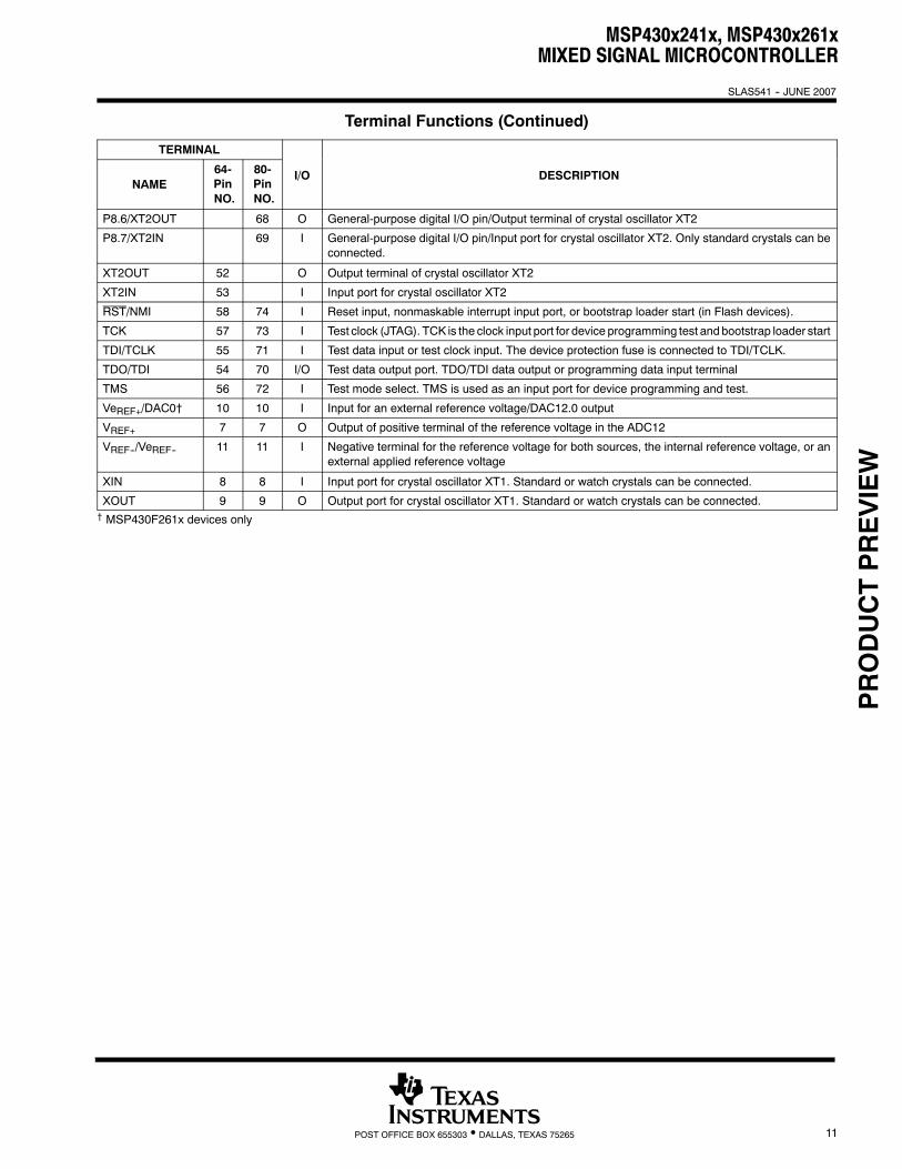
Terminal Functions (Continued)
TERMINAL
NAME64-PinNO.
80-PinNO.
I/O DESCRIPTION
P8.6/XT2OUT 68 O General-purpose digital I/O pin/Output terminal of crystal oscillator XT2
P8.7/XT2IN 69 I General-purpose digital I/O pin/Input port for crystal oscillator XT2. Only standard crystals can beconnected.
XT2OUT 52 O Output terminal of crystal oscillator XT2
XT2IN 53 I Input port for crystal oscillator XT2
RST/NMI 58 74 I Reset input, nonmaskable interrupt input port, or bootstrap loader start (in Flash devices).
TCK 57 73 I Test clock (JTAG). TCK is the clock input port for device programming test and bootstrap loader start
TDI/TCLK 55 71 I Test data input or test clock input. The device protection fuse is connected to TDI/TCLK.
TDO/TDI 54 70 I/O Test data output port. TDO/TDI data output or programming data input terminal
TMS 56 72 I Test mode select. TMS is used as an input port for device programming and test.
VeREF+/DAC0† 10 10 I Input for an external reference voltage/DAC12.0 output
VREF+ 7 7 O Output of positive terminal of the reference voltage in the ADC12
VREF--/VeREF-- 11 11 I Negative terminal for the reference voltage for both sources, the internal reference voltage, or anexternal applied reference voltage
XIN 8 8 I Input port for crystal oscillator XT1. Standard or watch crystals can be connected.
XOUT 9 9 O Output port for crystal oscillator XT1. Standard or watch crystals can be connected.† MSP430F261x devices only
PRODUCTPREVIEW
General-Purpose Register
Program Counter
Stack Pointer
Status Register
Constant Generator
General-Purpose Register
General-Purpose Register
General-Purpose Register
PC/R0
SP/R1
SR/CG1/R2
CG2/R3
R4
R5
R12
R13
General-Purpose Register
General-Purpose Register
R6
R7
General-Purpose Register
General-Purpose Register
R8
R9
General-Purpose Register
General-Purpose Register
R10
R11
General-Purpose Register
General-Purpose Register
R14
R15
MSP430x241x, MSP430x261xMIXED SIGNAL MICROCONTROLLER
SLAS541 -- JUNE 2007
12 POST OFFICE BOX 655303 • DALLAS, TEXAS 75265
short-form description
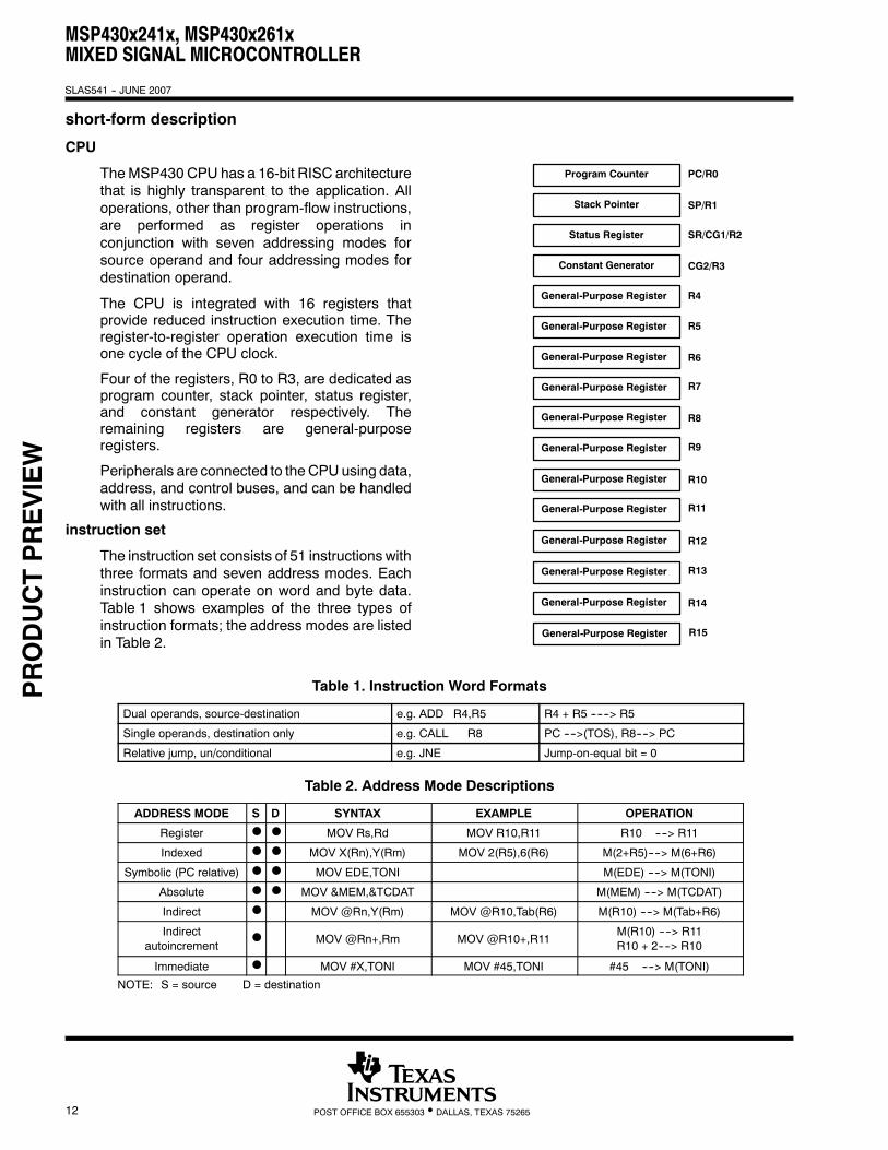
CPU
TheMSP430 CPU has a 16-bit RISC architecturethat is highly transparent to the application. Alloperations, other than program-flow instructions,are performed as register operations inconjunction with seven addressing modes forsource operand and four addressing modes fordestination operand.
The CPU is integrated with 16 registers thatprovide reduced instruction execution time. Theregister-to-register operation execution time isone cycle of the CPU clock.
Four of the registers, R0 to R3, are dedicated asprogram counter, stack pointer, status register,and constant generator respectively. Theremaining registers are general-purposeregisters.
Peripherals are connected to the CPU using data,address, and control buses, and can be handledwith all instructions.
instruction set
The instruction set consists of 51 instructions withthree formats and seven address modes. Eachinstruction can operate on word and byte data.Table 1 shows examples of the three types ofinstruction formats; the address modes are listedin Table 2.
Table 1. Instruction Word Formats
Dual operands, source-destination e.g. ADD R4,R5 R4 + R5 ------> R5
Single operands, destination only e.g. CALL R8 PC ---->(TOS), R8----> PC
Relative jump, un/conditional e.g. JNE Jump-on-equal bit = 0
Table 2. Address Mode Descriptions
ADDRESS MODE S D SYNTAX EXAMPLE OPERATION
Register D D MOV Rs,Rd MOV R10,R11 R10 ----> R11
Indexed D D MOV X(Rn),Y(Rm) MOV 2(R5),6(R6) M(2+R5)----> M(6+R6)
Symbolic (PC relative) D D MOV EDE,TONI M(EDE) ----> M(TONI)
Absolute D D MOV &MEM,&TCDAT M(MEM) ----> M(TCDAT)
Indirect D MOV @Rn,Y(Rm) MOV @R10,Tab(R6) M(R10) ----> M(Tab+R6)
Indirectautoincrement D MOV @Rn+,Rm MOV @R10+,R11
M(R10) ----> R11R10 + 2----> R10
Immediate D MOV #X,TONI MOV #45,TONI #45 ----> M(TONI)
NOTE: S = source D = destination
PRODUCTPREVIEW
MSP430x241x, MSP430x261xMIXED SIGNAL MICROCONTROLLER
SLAS541 -- JUNE 2007
13POST OFFICE BOX 655303 • DALLAS, TEXAS 75265
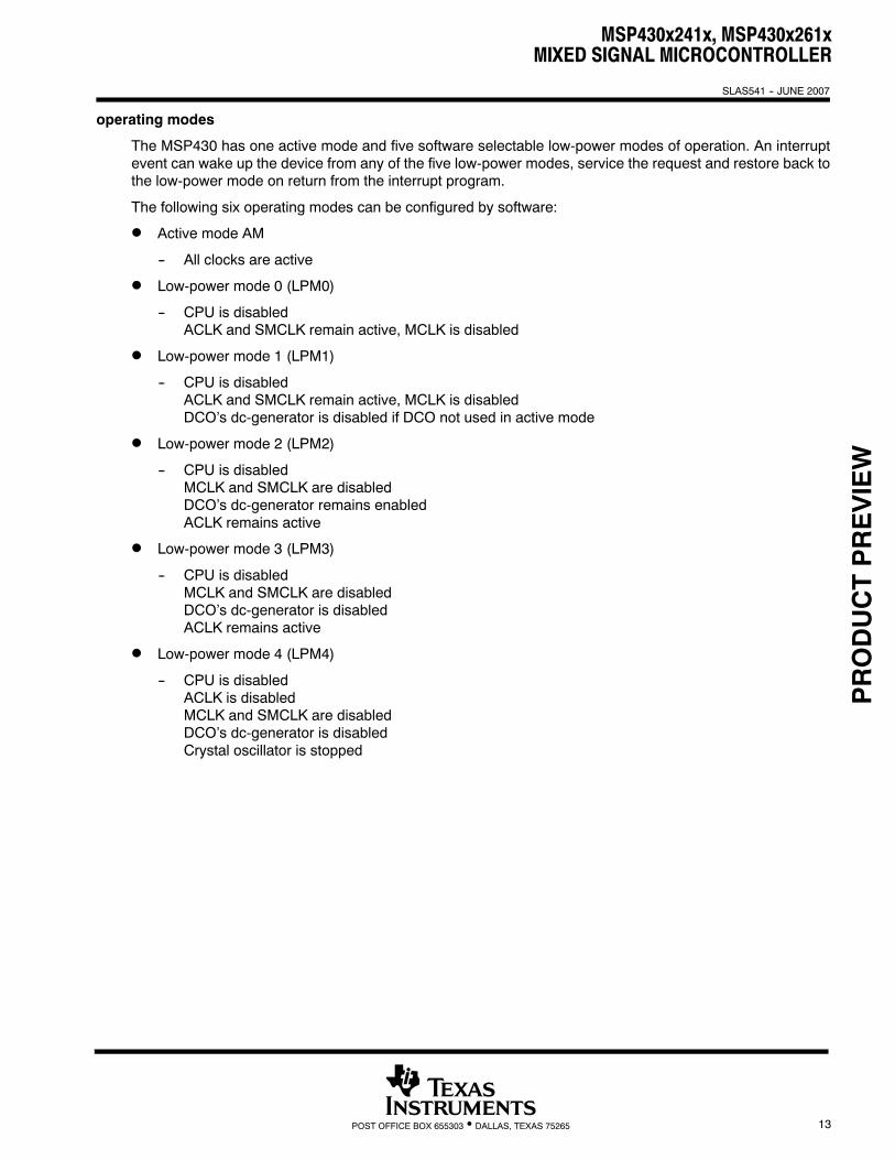
operating modes
The MSP430 has one active mode and five software selectable low-power modes of operation. An interruptevent can wake up the device from any of the five low-power modes, service the request and restore back tothe low-power mode on return from the interrupt program.
The following six operating modes can be configured by software:
D Active mode AM
-- All clocks are active
D Low-power mode 0 (LPM0)
-- CPU is disabledACLK and SMCLK remain active, MCLK is disabled
D Low-power mode 1 (LPM1)
-- CPU is disabledACLK and SMCLK remain active, MCLK is disabledDCO’s dc-generator is disabled if DCO not used in active mode
D Low-power mode 2 (LPM2)
-- CPU is disabledMCLK and SMCLK are disabledDCO’s dc-generator remains enabledACLK remains active
D Low-power mode 3 (LPM3)
-- CPU is disabledMCLK and SMCLK are disabledDCO’s dc-generator is disabledACLK remains active
D Low-power mode 4 (LPM4)
-- CPU is disabledACLK is disabledMCLK and SMCLK are disabledDCO’s dc-generator is disabledCrystal oscillator is stopped
PRODUCTPREVIEW
MSP430x241x, MSP430x261xMIXED SIGNAL MICROCONTROLLER
SLAS541 -- JUNE 2007
14 POST OFFICE BOX 655303 • DALLAS, TEXAS 75265
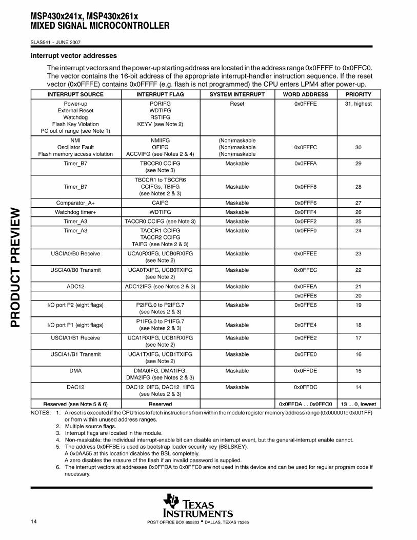
interrupt vector addresses
The interrupt vectors and thepower-upstartingaddressare located in theaddress range0x0FFFF to 0x0FFC0.The vector contains the 16-bit address of the appropriate interrupt-handler instruction sequence. If the resetvector (0x0FFFE) contains 0x0FFFF (e.g. flash is not programmed) the CPU enters LPM4 after power-up.INTERRUPT SOURCE INTERRUPT FLAG SYSTEM INTERRUPT WORD ADDRESS PRIORITY
Power-upExternal ResetWatchdog
Flash Key ViolationPC out of range (see Note 1)
PORIFGWDTIFGRSTIFG
KEYV (see Note 2)
Reset 0x0FFFE 31, highest
NMIOscillator Fault
Flash memory access violation
NMIIFGOFIFG
ACCVIFG (see Notes 2 & 4)
(Non)maskable(Non)maskable(Non)maskable
0x0FFFC 30
Timer_B7 TBCCR0 CCIFG(see Note 3)
Maskable 0x0FFFA 29
Timer_B7TBCCR1 to TBCCR6CCIFGs, TBIFG(see Notes 2 & 3)
Maskable 0x0FFF8 28
Comparator_A+ CAIFG Maskable 0x0FFF6 27
Watchdog timer+ WDTIFG Maskable 0x0FFF4 26
Timer_A3 TACCR0 CCIFG (see Note 3) Maskable 0x0FFF2 25
Timer_A3 TACCR1 CCIFGTACCR2 CCIFG
TAIFG (see Note 2 & 3)
Maskable 0x0FFF0 24
USCIA0/B0 Receive UCA0RXIFG, UCB0RXIFG(see Note 2)
Maskable 0x0FFEE 23
USCIA0/B0 Transmit UCA0TXIFG, UCB0TXIFG(see Note 2)
Maskable 0x0FFEC 22
ADC12 ADC12IFG (see Notes 2 & 3) Maskable 0x0FFEA 21
0x0FFE8 20
I/O port P2 (eight flags) P2IFG.0 to P2IFG.7(see Notes 2 & 3)
Maskable 0x0FFE6 19
I/O port P1 (eight flags)P1IFG.0 to P1IFG.7(see Notes 2 & 3) Maskable 0x0FFE4 18
USCIA1/B1 Receive UCA1RXIFG, UCB1RXIFG(see Note 2)
Maskable 0x0FFE2 17
USCIA1/B1 Transmit UCA1TXIFG, UCB1TXIFG(see Note 2)
Maskable 0x0FFE0 16
DMA DMA0IFG, DMA1IFG,DMA2IFG (see Notes 2 & 3)
Maskable 0x0FFDE 15
DAC12 DAC12_0IFG, DAC12_1IFG(see Notes 2 & 3)
Maskable 0x0FFDC 14
Reserved (see Note 5 & 6) Reserved 0x0FFDA 0x0FFC0 13 0 lowestReserved (see Note 5 & 6) Reserved 0x0FFDA ... 0x0FFC0 13 ... 0, lowest
NOTES: 1. A reset is executed if theCPU tries to fetch instructions fromwithin themodule registermemoryaddress range (0x00000 to0x001FF)or from within unused address ranges.
2. Multiple source flags.3. Interrupt flags are located in the module.4. Non-maskable: the individual interrupt-enable bit can disable an interrupt event, but the general-interrupt enable cannot.5. The address 0x0FFBE is used as bootstrap loader security key (BSLSKEY).
A 0x0AA55 at this location disables the BSL completely.A zero disables the erasure of the flash if an invalid password is supplied.
6. The interrupt vectors at addresses 0x0FFDA to 0x0FFC0 are not used in this device and can be used for regular program code ifnecessary.
PRODUCTPREVIEW
MSP430x241x, MSP430x261xMIXED SIGNAL MICROCONTROLLER
SLAS541 -- JUNE 2007
15POST OFFICE BOX 655303 • DALLAS, TEXAS 75265
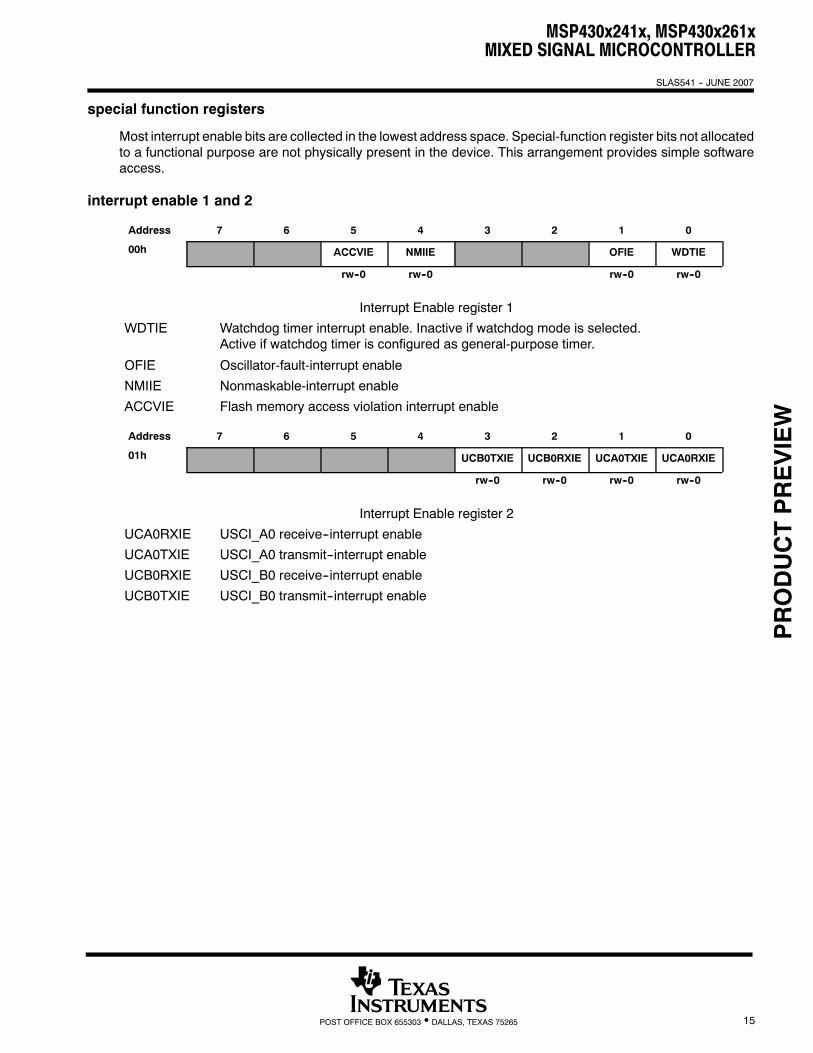
special function registers
Most interrupt enable bits are collected in the lowest address space. Special-function register bits not allocatedto a functional purpose are not physically present in the device. This arrangement provides simple softwareaccess.
interrupt enable 1 and 2
Address 7 6 5 4 3 2 1 0
00h ACCVIE NMIIE OFIE WDTIE
rw--0 rw--0 rw--0 rw--0
Interrupt Enable register 1
WDTIE Watchdog timer interrupt enable. Inactive if watchdog mode is selected.Active if watchdog timer is configured as general-purpose timer.
OFIE Oscillator-fault-interrupt enable
NMIIE Nonmaskable-interrupt enable
ACCVIE Flash memory access violation interrupt enable
Address 7 6 5 4 3 2 1 0
01h UCB0TXIE UCB0RXIE UCA0TXIE UCA0RXIE
rw--0 rw--0 rw--0 rw--0
Interrupt Enable register 2
UCA0RXIE USCI_A0 receive--interrupt enable
UCA0TXIE USCI_A0 transmit--interrupt enable
UCB0RXIE USCI_B0 receive--interrupt enable
UCB0TXIE USCI_B0 transmit--interrupt enable
PRODUCTPREVIEW
MSP430x241x, MSP430x261xMIXED SIGNAL MICROCONTROLLER
SLAS541 -- JUNE 2007
16 POST OFFICE BOX 655303 • DALLAS, TEXAS 75265
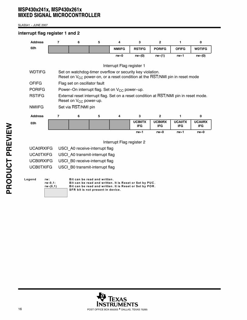
interrupt flag register 1 and 2
Address 7 6 5 4 3 2 1 0
02h NMIIFG RSTIFG PORIFG OFIFG WDTIFG
rw--0 rw--(0) rw--(1) rw--1 rw--(0)
Interrupt Flag register 1
WDTIFG Set on watchdog-timer overflow or security key violation.Reset on VCC power-on, or a reset condition at the RST/NMI pin in reset mode
OFIFG Flag set on oscillator fault
PORIFG Power--On interrupt flag. Set on VCC power--up.
RSTIFG External reset interrupt flag. Set on a reset condition at RST/NMI pin in reset mode.Reset on VCC power-up.
NMIIFG Set via RST/NMI pin
Address 7 6 5 4 3 2 1 0
03h UCB0TXIFG
UCB0RXIFG
UCA0TXIFG
UCA0RXIFG
rw--1 rw--0 rw--1 rw--0
Interrupt Flag register 2
UCA0RXIFG USCI_A0 receive-interrupt flag
UCA0TXIFG USCI_A0 transmit-interrupt flag
UCB0RXIFG USCI_B0 receive-interrupt flag
UCB0TXIFG USCI_B0 transmit-interrupt flag
Legend rw : Bit can be read and w ritten .rw -0,1: B it can be read and w ritten . It is Reset or Set by PUC .rw -(0,1) B it can be read and w ritten . It is Reset or Set by PO R .
SFR bit is not present in device .PRODUCTPREVIEW
MSP430x241x, MSP430x261xMIXED SIGNAL MICROCONTROLLER
SLAS541 -- JUNE 2007
17POST OFFICE BOX 655303 • DALLAS, TEXAS 75265
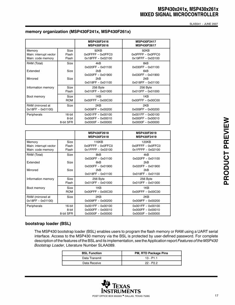
memory organization (MSP430F241x, MSP430F261x)
MSP430F2416MSP430F2616
MSP430F2417MSP430F2617
MemoryMain: interrupt vectorMain: code memory
SizeFlashFlash
92KB0x0FFFF -- 0x0FFC00x18FFF -- 0x02100
92KB0x0FFFF -- 0x0FFC00x19FFF -- 0x03100
RAM (Total)
Extended
Mirrored
Size
Size
Size
4kB0x020FF -- 0x01100
2kB0x020FF -- 0x01900
2kB0x018FF -- 0x01100
8kB0x030FF -- 0x01100
6kB0x030FF -- 0x01900
2kB0x018FF -- 0x01100
Information memory SizeFlash
256 Byte0x010FF -- 0x01000
256 Byte0x010FF -- 0x01000
Boot memory SizeROM
1KB0x00FFF -- 0x00C00
1KB0x00FFF -- 0x00C00
RAM (mirrored at0x18FF -- 0x01100)
Size 2KB0x009FF -- 0x00200
2KB0x009FF -- 0x00200
Peripherals 16-bit8-bit
8-bit SFR
0x001FF -- 0x001000x000FF -- 0x000100x0000F -- 0x00000
0x001FF -- 0x001000x000FF -- 0x000100x0000F -- 0x00000
MSP430F2618MSP430F2418
MSP430F2619MSP430F2419
MemoryMain: interrupt vectorMain: code memory
SizeFlashFlash
116KB0x0FFFF -- 0x0FFC00x1FFFF -- 0x03100
120KB0x0FFFF -- 0x0FFC00x1FFFF -- 0x02100
RAM (Total)
Extended
Mirrored
Size
Size
Size
8kB0x030FF -- 0x01100
6kB0x030FF -- 0x01900
2kB0x018FF -- 0x01100
4kB0x020FF -- 0x01100
2kB0x020FF -- 0x01900
2kB0x018FF -- 0x01100
Information memory SizeFlash
256 Byte0x010FF -- 0x01000
256 Byte0x010FF -- 0x01000
Boot memory SizeROM
1KB0x00FFF -- 0x00C00
1KB0x00FFF -- 0x00C00
RAM (mirrored at0x18FF -- 0x01100)
Size 2KB0x009FF -- 0x00200
2KB0x009FF -- 0x00200
Peripherals 16-bit8-bit
8-bit SFR
0x001FF -- 0x001000x000FF -- 0x000100x0000F -- 0x00000
0x001FF -- 0x001000x000FF -- 0x000100x0000F -- 0x00000
bootstrap loader (BSL)
The MSP430 bootstrap loader (BSL) enables users to program the flash memory or RAM using a UART serialinterface. Access to the MSP430 memory via the BSL is protected by user-defined password. For completedescriptionof the features of theBSLand its implementation, see theApplication reportFeaturesof theMSP430Bootstrap Loader, Literature Number SLAA089.
BSL Function PM, RTD Package Pins
Data Transmit 13 - P1.1
Data Receive 22 - P2.2
PRODUCTPREVIEW
MSP430x241x, MSP430x261xMIXED SIGNAL MICROCONTROLLER
SLAS541 -- JUNE 2007
18 POST OFFICE BOX 655303 • DALLAS, TEXAS 75265
flash memory
The flash memory can be programmed via the JTAG port, the bootstrap loader, or in-system by the CPU. TheCPUcan performsingle-byte and single-wordwrites to the flashmemory. Features of the flashmemory include:
D Flash memory has n segments of main memory and four segments of information memory (A to D) of64 bytes each. Each segment in main memory is 512 bytes in size.
D Segments 0 to n may be erased in one step, or each segment may be individually erased.
D Segments A to D can be erased individually, or as a group with segments 0--n.Segments A to D are also called information memory.
D Segment A contains calibration data. After reset segment A is protected against programming or erasing.It can be unlocked but care should be taken not to erase this segment if the calibration data is required.
D Flash content integrity check with marginal read modes.
peripherals
Peripherals are connected to the CPU through data, address, and control busses and can be handled usingall instructions. For complete module descriptions, see the MSP430x2xx Family User’s Guide, TI literaturenumber SLAU144.
DMA controller
The DMA controller allows movement of data from one memory address to another without CPU intervention.For example, theDMAcontroller can be used tomove data from the ADC12 conversionmemory to RAM.Usingthe DMA controller can increase the throughput of peripheral modules. The DMA controller reduces systempower consumption by allowing the CPU to remain in sleep mode without having to awaken to move data toor from a peripheral.
oscillator and system clock
The clock system in the MSP430x241x and MSP43x261x family of devices is supported by the basic clockmodule that includes support for a 32768-Hz watch crystal oscillator, an internal very low power, low frequencyoscillator, an internal digitally-controlledoscillator (DCO),andahigh frequencycrystal oscillator.Thebasic clockmodule is designed tomeet the requirements of both low system cost and low power consumption. The internalDCO provides a fast turn-on clock source and stabilizes in less than 1 μs. The basic clock module provides thefollowing clock signals:
D Auxiliary clock (ACLK), sourced from a 32768-Hz watch crystal, a high frequency crystal, or a very lowpower LF oscillator.
D Main clock (MCLK), the system clock used by the CPU.D Sub-Main clock (SMCLK), the sub-system clock used by the peripheral modules.
The DCO settings to calibrate the DCO output frequency are stored in the information memory segment A.
PRODUCTPREVIEW
MSP430x241x, MSP430x261xMIXED SIGNAL MICROCONTROLLER
SLAS541 -- JUNE 2007
19POST OFFICE BOX 655303 • DALLAS, TEXAS 75265
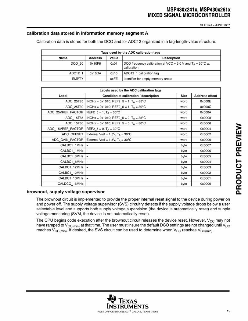
calibration data stored in information memory segment A
Calibration data is stored for both the DCO and for ADC12 organized in a tag-length-value structure.
Tags used by the ADC calibration tags
Name Address Value Description
DCO_30 0x10F6 0x01 DCO frequency calibration at VCC = 3.0 V and TA = 30°C atcalibration
ADC12_1 0x10DA 0x10 ADC12_1 calibration tag
EMPTY -- 0xFE Identifier for empty memory areas
Labels used by the ADC calibration tags
Label Condition at calibration / description Size Address offset
ADC_25T85 INCHx = 0x1010; REF2_5 = 1, TA = 85°C word 0x000E
ADC_25T30 INCHx = 0x1010; REF2_5 = 1, TA = 30°C word 0x000C
ADC_25VREF_FACTOR REF2_5 = 1, TA = 30°C word 0x000A
ADC_15T85 INCHx = 0x1010; REF2_5 = 0, TA = 85°C word 0x0008
ADC_15T30 INCHx = 0x1010; REF2_5 = 0, TA = 30°C word 0x0006
ADC_15VREF_FACTOR REF2_5 = 0, TA = 30°C word 0x0004
ADC_OFFSET External Vref = 1.5V, TA = 30°C word 0x0002
ADC_GAIN_FACTOR External Vref = 1.5V, TA = 30°C word 0x0000
CALBC1_1MHz -- byte 0x0007
CALBC1_1MHz -- byte 0x0006
CALBC1_8MHz -- byte 0x0005
CALBC1_8MHz -- byte 0x0004
CALBC1_12MHz -- byte 0x0003
CALBC1_12MHz -- byte 0x0002
CALBC1_16MHz -- byte 0x0001
CALDCO_16MHz -- byte 0x0000
brownout, supply voltage supervisor
The brownout circuit is implemented to provide the proper internal reset signal to the device during power onand power off. The supply voltage supervisor (SVS) circuitry detects if the supply voltage drops below a userselectable level and supports both supply voltage supervision (the device is automatically reset) and supplyvoltage monitoring (SVM, the device is not automatically reset).
The CPU begins code execution after the brownout circuit releases the device reset. However, VCC may nothave ramped to VCC(min) at that time. The user must insure the default DCO settings are not changed until VCCreaches VCC(min). If desired, the SVS circuit can be used to determine when VCC reaches VCC(min).
PRODUCTPREVIEW
MSP430x241x, MSP430x261xMIXED SIGNAL MICROCONTROLLER
SLAS541 -- JUNE 2007
20 POST OFFICE BOX 655303 • DALLAS, TEXAS 75265
digital I/O
There are up to eight 8-bit I/O ports implemented—ports P1 through P8:
D All individual I/O bits are independently programmable.D Any combination of input, output, and interrupt conditions is possible.D Edge-selectable interrupt input capability for all eight bits of ports P1 and P2.D Read/write access to port-control registers is supported by all instructions.D Each I/O has an individually programmable pullup/pulldown resistor.D Ports P7/P8 can be accessed word wise.
watchdog timer+
The primary function of the watchdog timer (WDT+) module is to perform a controlled system restart after asoftware problem occurs. If the selected time interval expires, a system reset is generated. If the watchdogfunction is not needed in an application, the module can be configured as an interval timer and can generateinterrupts at selected time intervals.
hardware multiplierThe multiplication operation is supported by a dedicated peripheral module. The module performs 16×16,16×8, 8×16, and 8×8 bit operations. Themodule is capable of supporting signed and unsignedmultiplicationaswell as signedandunsignedmultiply andaccumulate operations. The result of an operation canbeaccessedimmediately after the operands have been loaded into the peripheral registers. No additional clock cycles arerequired.
USCI
The universal serial communicating interface (USCI) modules are used for serial data communication. TheUSCI module supports synchronous communication protocols like SPI (3 or 4 pin), I2C and asynchronouscombination protocols like UART, enhanced UART with automatic baudrate detection (LIN), and IrDA.
The USCI A module provides support for SPI (3 or 4 pin), UART, enhanced UART and IrDA.
The USCI B module provides support for SPI (3 or 4 pin) and I2C.
PRODUCTPREVIEW
MSP430x241x, MSP430x261xMIXED SIGNAL MICROCONTROLLER
SLAS541 -- JUNE 2007
21POST OFFICE BOX 655303 • DALLAS, TEXAS 75265
timer_A3
Timer_A3 is a 16-bit timer/counter with three capture/compare registers. Timer_A3 can support multiplecapture/compares, PWM outputs, and interval timing. Timer_A3 also has extensive interrupt capabilities.Interrupts may be generated from the counter on overflow conditions and from each of the capture/compareregisters.
Timer_A3 Signal Connections
Input Pin Number Device Input Signal Module Input Name Module Block Module Output Signal Output Pin Number
12 - P1.0 TACLK TACLK
ACLK ACLKTimer NA
SMCLK SMCLKTimer NA
21 - P2.1 TAINCLK INCLK
13 - P1.1 TA0 CCI0A 13 - P1.1
22 - P2.2 TA0 CCI0BCCR0 TA0
17 - P1.5
DVSS GNDCCR0 TA0
27 - P2.7
DVCC VCC14 - P1.2 TA1 CCI1A 14 - P1.2
CAOUT (internal) CCI1BCCR1
18 - P1.6
DVSS GNDCCR1
TA123 - P2.3
DVCC VCCTA1
ADC12 (internal)
DAC12_0 (internal)
DAC12_1 (internal)
15 - P1.3 TA2 CCI2A 15 - P1.3
ACLK (internal) CCI2BCCR2 TA2
19 - P1.7
DVSS GNDCCR2 TA2
24 - P2.4
DVCC VCC
PRODUCTPREVIEW
MSP430x241x, MSP430x261xMIXED SIGNAL MICROCONTROLLER
SLAS541 -- JUNE 2007
22 POST OFFICE BOX 655303 • DALLAS, TEXAS 75265
timer_B7
Timer_B7 is a 16-bit timer/counter with seven capture/compare registers. Timer_B7 can support multiplecapture/compares, PWM outputs, and interval timing. Timer_B7 also has extensive interrupt capabilities.Interrupts may be generated from the counter on overflow conditions and from each of the capture/compareregisters.
Timer_B3/B7 Signal Connections†
Input Pin Number Device Input Signal Module Input Name Module Block Module Output Signal Output Pin Number
43 - P4.7 TBCLK TBCLK
ACLK ACLKTimer NA
SMCLK SMCLKTimer NA
43 - P4.7 TBCLK INCLK
36 - P4.0 TB0 CCI0A 36 - P4.0
36 - P4.0 TB0 CCI0BCCR0 TB0
ADC12 (internal)
DVSS GNDCCR0 TB0
DVCC VCC37 - P4.1 TB1 CCI1A 37 - P4.1
37 - P4.1 TB1 CCI1BCCR1 TB1
ADC12 (internal)
DVSS GNDCCR1 TB1
DVCC VCC38 - P4.2 TB2 CCI2A 38 - P4.2
38 - P4.2 TB2 CCI2BCCR2 TB2
DAC_0(internal)
DVSS GNDCCR2 TB2
DAC_1(internal)
DVCC VCC39 - P4.3 TB3 CCI3A 39 - P4.3
39 - P4.3 TB3 CCI3BCCR3 TB3
DVSS GNDCCR3 TB3
DVCC VCC40 - P4.4 TB4 CCI4A 40 - P4.4
40 - P4.4 TB4 CCI4BCCR4 TB4
DVSS GNDCCR4 TB4
DVCC VCC41 - P4.5 TB5 CCI5A 41 - P4.5
41 - P4.5 TB5 CCI5BCCR5 TB5
DVSS GNDCCR5 TB5
DVCC VCC42 - P4.6 TB6 CCI6A 42 - P4.6
ACLK (internal) CCI6BCCR6 TB6
DVSS GNDCCR6 TB6
DVCC VCC
PRODUCTPREVIEW
MSP430x241x, MSP430x261xMIXED SIGNAL MICROCONTROLLER
SLAS541 -- JUNE 2007
23POST OFFICE BOX 655303 • DALLAS, TEXAS 75265
comparator_A+
Theprimary function of the comparator_A+module is to support precision slope analog--to--digital conversions,battery-voltage supervision, and monitoring of external analog signals.
ADC12The ADC12 module supports fast, 12-bit analog-to-digital conversions. The module implements a 12-bit SARcore, sample select control, reference generator, and a 16-word conversion-and-control buffer. Theconversion-and-control buffer allows up to 16 independent ADC samples to be converted and stored withoutany CPU intervention.
DAC12
The DAC12 module is a 12-bit, R-ladder, voltage output DAC. The DAC12 may be used in 8- or 12-bit mode,andmay be used in conjunction with the DMA controller. Whenmultiple DAC12modules are present, theymaybe grouped together for synchronous operation.
PRODUCTPREVIEW
MSP430x241x, MSP430x261xMIXED SIGNAL MICROCONTROLLER
SLAS541 -- JUNE 2007
24 POST OFFICE BOX 655303 • DALLAS, TEXAS 75265
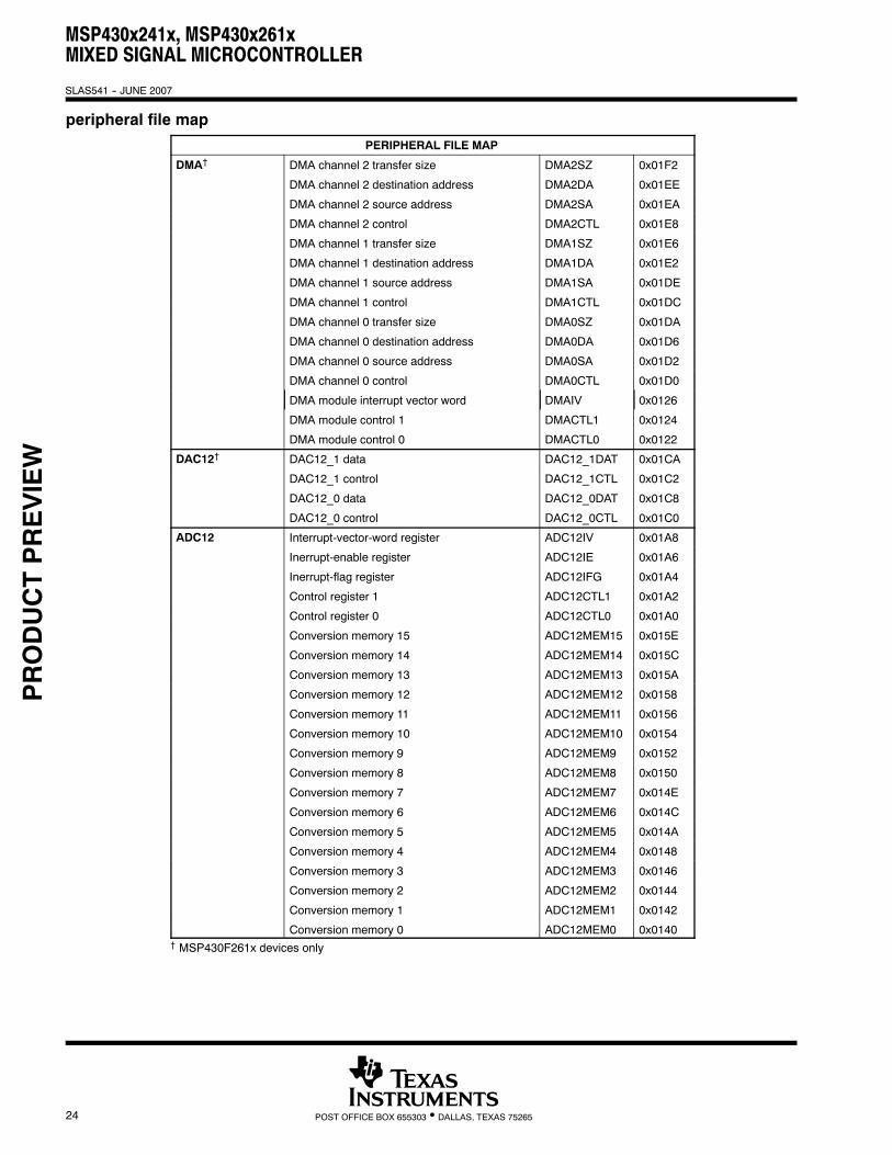
peripheral file map
PERIPHERAL FILE MAP
DMA† DMA channel 2 transfer size DMA2SZ 0x01F2
DMA channel 2 destination address DMA2DA 0x01EE
DMA channel 2 source address DMA2SA 0x01EA
DMA channel 2 control DMA2CTL 0x01E8
DMA channel 1 transfer size DMA1SZ 0x01E6
DMA channel 1 destination address DMA1DA 0x01E2
DMA channel 1 source address DMA1SA 0x01DE
DMA channel 1 control DMA1CTL 0x01DC
DMA channel 0 transfer size DMA0SZ 0x01DA
DMA channel 0 destination address DMA0DA 0x01D6
DMA channel 0 source address DMA0SA 0x01D2
DMA channel 0 control DMA0CTL 0x01D0
DMA module interrupt vector word DMAIV 0x0126
DMA module control 1 DMACTL1 0x0124
DMA module control 0 DMACTL0 0x0122
DAC12† DAC12_1 data DAC12_1DAT 0x01CA
DAC12_1 control DAC12_1CTL 0x01C2
DAC12_0 data DAC12_0DAT 0x01C8
DAC12_0 control DAC12_0CTL 0x01C0
ADC12 Interrupt-vector-word register ADC12IV 0x01A8
Inerrupt-enable register ADC12IE 0x01A6
Inerrupt-flag register ADC12IFG 0x01A4
Control register 1 ADC12CTL1 0x01A2
Control register 0 ADC12CTL0 0x01A0
Conversion memory 15 ADC12MEM15 0x015E
Conversion memory 14 ADC12MEM14 0x015C
Conversion memory 13 ADC12MEM13 0x015A
Conversion memory 12 ADC12MEM12 0x0158
Conversion memory 11 ADC12MEM11 0x0156
Conversion memory 10 ADC12MEM10 0x0154
Conversion memory 9 ADC12MEM9 0x0152
Conversion memory 8 ADC12MEM8 0x0150
Conversion memory 7 ADC12MEM7 0x014E
Conversion memory 6 ADC12MEM6 0x014C
Conversion memory 5 ADC12MEM5 0x014A
Conversion memory 4 ADC12MEM4 0x0148
Conversion memory 3 ADC12MEM3 0x0146
Conversion memory 2 ADC12MEM2 0x0144
Conversion memory 1 ADC12MEM1 0x0142
Conversion memory 0 ADC12MEM0 0x0140† MSP430F261x devices only
PRODUCTPREVIEW
MSP430x241x, MSP430x261xMIXED SIGNAL MICROCONTROLLER
SLAS541 -- JUNE 2007
25POST OFFICE BOX 655303 • DALLAS, TEXAS 75265
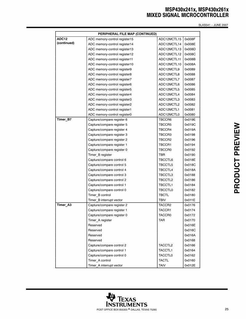
PERIPHERAL FILE MAP (CONTINUED)
ADC12 ADC memory-control register15 ADC12MCTL15 0x008F(continued) ADC memory-control register14 ADC12MCTL14 0x008E
ADC memory-control register13 ADC12MCTL13 0x008D
ADC memory-control register12 ADC12MCTL12 0x008C
ADC memory-control register11 ADC12MCTL11 0x008B
ADC memory-control register10 ADC12MCTL10 0x008A
ADC memory-control register9 ADC12MCTL9 0x0089
ADC memory-control register8 ADC12MCTL8 0x0088
ADC memory-control register7 ADC12MCTL7 0x0087
ADC memory-control register6 ADC12MCTL6 0x0086
ADC memory-control register5 ADC12MCTL5 0x0085
ADC memory-control register4 ADC12MCTL4 0x0084
ADC memory-control register3 ADC12MCTL3 0x0083
ADC memory-control register2 ADC12MCTL2 0x0082
ADC memory-control register1 ADC12MCTL1 0x0081
ADC memory-control register0 ADC12MCTL0 0x0080Timer_B7 Capture/compare register 6 TBCCR6 0x019E_
Capture/compare register 5 TBCCR5 0x019C
Capture/compare register 4 TBCCR4 0x019A
Capture/compare register 3 TBCCR3 0x0198
Capture/compare register 2 TBCCR2 0x0196
Capture/compare register 1 TBCCR1 0x0194
Capture/compare register 0 TBCCR0 0x0192
Timer_B register TBR 0x0190
Capture/compare control 6 TBCCTL6 0x018E
Capture/compare control 5 TBCCTL5 0x018C
Capture/compare control 4 TBCCTL4 0x018A
Capture/compare control 3 TBCCTL3 0x0188
Capture/compare control 2 TBCCTL2 0x0186
Capture/compare control 1 TBCCTL1 0x0184
Capture/compare control 0 TBCCTL0 0x0182
Timer_B control TBCTL 0x0180
Timer_B interrupt vector TBIV 0x011ETimer_A3 Capture/compare register 2 TACCR2 0x0176_
Capture/compare register 1 TACCR1 0x0174
Capture/compare register 0 TACCR0 0x0172
Timer_A register TAR 0x0170
Reserved 0x016E
Reserved 0x016C
Reserved 0x016A
Reserved 0x0168
Capture/compare control 2 TACCTL2 0x0166
Capture/compare control 1 TACCTL1 0x0164
Capture/compare control 0 TACCTL0 0x0162
Timer_A control TACTL 0x0160
Timer_A interrupt vector TAIV 0x012E
PRODUCTPREVIEW
MSP430x241x, MSP430x261xMIXED SIGNAL MICROCONTROLLER
SLAS541 -- JUNE 2007
26 POST OFFICE BOX 655303 • DALLAS, TEXAS 75265
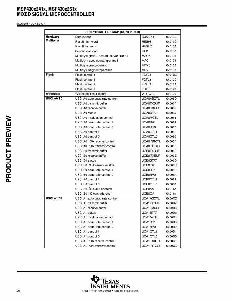
PERIPHERAL FILE MAP (CONTINUED)
Hardware Sum extend SUMEXT 0x013EMultiplier Result high word RESHI 0x013C
Result low word RESLO 0x013A
Second operand OP2 0x0138
Multiply signed + accumulate/operand1 MACS 0x0136
Multiply + accumulate/operand1 MAC 0x0134
Multiply signed/operand1 MPYS 0x0132
Multiply unsigned/operand1 MPY 0x0130Flash Flash control 4 FCTL4 0x01BE
Flash control 3 FCTL3 0x012C
Flash control 2 FCTL2 0x012A
Flash control 1 FCTL1 0x0128
Watchdog Watchdog Timer control WDTCTL 0x0120
USCI A0/B0 USCI A0 auto baud rate control UCA0ABCTL 0x005D/
USCI A0 transmit buffer UCA0TXBUF 0x0067
USCI A0 receive buffer UCA0RXBUF 0x0066
USCI A0 status UCA0STAT 0x0065
USCI A0 modulation control UCA0MCTL 0x0064
USCI A0 baud rate control 1 UCA0BR1 0x0063
USCI A0 baud rate control 0 UCA0BR0 0x0062
USCI A0 control 1 UCA0CTL1 0x0061
USCI A0 control 0 UCA0CTL0 0x0060
USCI A0 IrDA receive control UCA0IRRCTL 0x005F
USCI A0 IrDA transmit control UCA0IRTCLT 0x005E
USCI B0 transmit buffer UCB0TXBUF 0x006F
USCI B0 receive buffer UCB0RXBUF 0x006E
USCI B0 status UCB0STAT 0x006D
USCI B0 I2C Interrupt enable UCB0CIE 0x006C
USCI B0 baud rate control 1 UCB0BR1 0x006B
USCI B0 baud rate control 0 UCB0BR0 0x006A
USCI B0 control 1 UCB0CTL1 0x0069
USCI B0 control 0 UCB0CTL0 0x0068
USCI B0 I2C slave address UCB0SA 0x011A
USCI B0 I2C own address UCB0OA 0x0118
USCI A1/B1 USCI A1 auto baud rate control UCA1ABCTL 0x00CD/
USCI A1 transmit buffer UCA1TXBUF 0x00D7
USCI A1 receive buffer UCA1RXBUF 0x00D6
USCI A1 status UCA1STAT 0x00D5
USCI A1 modulation control UCA1MCTL 0x00D4
USCI A1 baud rate control 1 UCA1BR1 0x00D3
USCI A1 baud rate control 0 UCA1BR0 0x00D2
USCI A1 control 1 UCA1CTL1 0x00D1
USCI A1 control 0 UCA1CTL0 0x00D0
USCI A1 IrDA receive control UCA1IRRCTL 0x00CF
USCI A1 IrDA transmit control UCA1IRTCLT 0x00CE
PRODUCTPREVIEW
MSP430x241x, MSP430x261xMIXED SIGNAL MICROCONTROLLER
SLAS541 -- JUNE 2007
27POST OFFICE BOX 655303 • DALLAS, TEXAS 75265
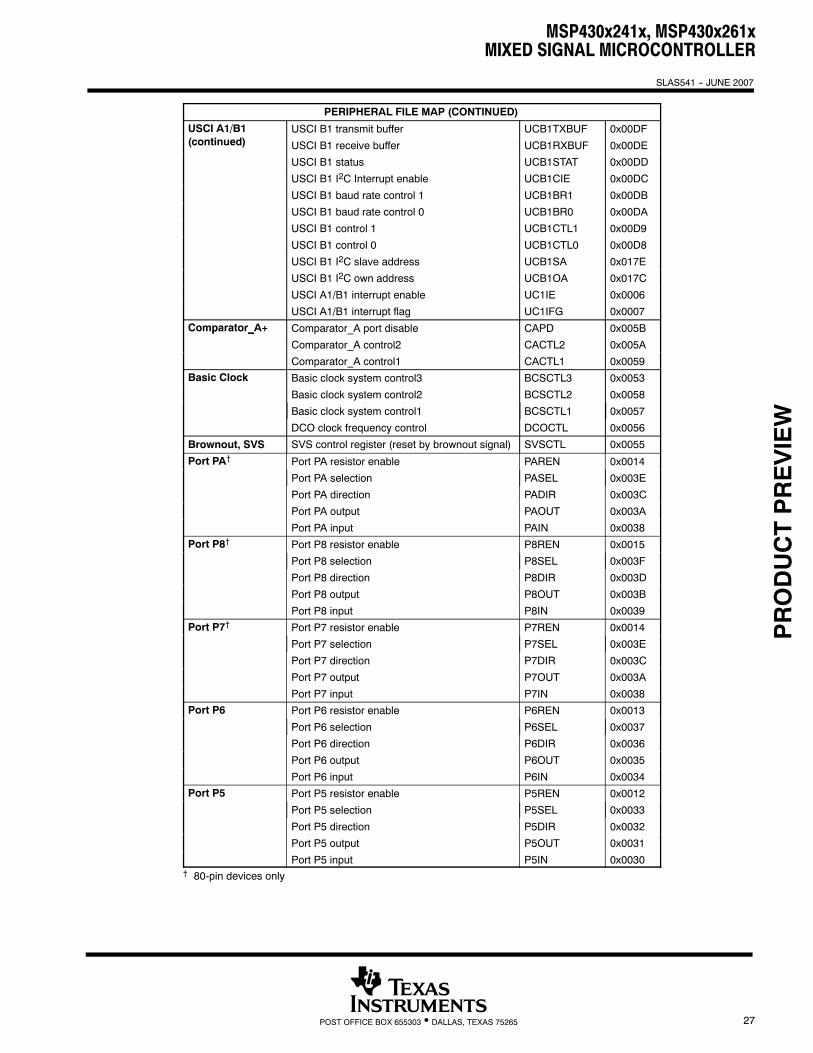
PERIPHERAL FILE MAP (CONTINUED)
USCI A1/B1 USCI B1 transmit buffer UCB1TXBUF 0x00DF/(continued) USCI B1 receive buffer UCB1RXBUF 0x00DE
USCI B1 status UCB1STAT 0x00DD
USCI B1 I2C Interrupt enable UCB1CIE 0x00DC
USCI B1 baud rate control 1 UCB1BR1 0x00DB
USCI B1 baud rate control 0 UCB1BR0 0x00DA
USCI B1 control 1 UCB1CTL1 0x00D9
USCI B1 control 0 UCB1CTL0 0x00D8
USCI B1 I2C slave address UCB1SA 0x017E
USCI B1 I2C own address UCB1OA 0x017C
USCI A1/B1 interrupt enable UC1IE 0x0006
USCI A1/B1 interrupt flag UC1IFG 0x0007
Comparator_A+ Comparator_A port disable CAPD 0x005Bp _
Comparator_A control2 CACTL2 0x005A
Comparator_A control1 CACTL1 0x0059Basic Clock Basic clock system control3 BCSCTL3 0x0053
Basic clock system control2 BCSCTL2 0x0058
Basic clock system control1 BCSCTL1 0x0057
DCO clock frequency control DCOCTL 0x0056
Brownout, SVS SVS control register (reset by brownout signal) SVSCTL 0x0055
Port PA† Port PA resistor enable PAREN 0x0014
Port PA selection PASEL 0x003E
Port PA direction PADIR 0x003C
Port PA output PAOUT 0x003A
Port PA input PAIN 0x0038
Port P8† Port P8 resistor enable P8REN 0x0015
Port P8 selection P8SEL 0x003F
Port P8 direction P8DIR 0x003D
Port P8 output P8OUT 0x003B
Port P8 input P8IN 0x0039
Port P7† Port P7 resistor enable P7REN 0x0014
Port P7 selection P7SEL 0x003E
Port P7 direction P7DIR 0x003C
Port P7 output P7OUT 0x003A
Port P7 input P7IN 0x0038
Port P6 Port P6 resistor enable P6REN 0x0013
Port P6 selection P6SEL 0x0037
Port P6 direction P6DIR 0x0036
Port P6 output P6OUT 0x0035
Port P6 input P6IN 0x0034
Port P5 Port P5 resistor enable P5REN 0x0012
Port P5 selection P5SEL 0x0033
Port P5 direction P5DIR 0x0032
Port P5 output P5OUT 0x0031
Port P5 input P5IN 0x0030† 80-pin devices only
PRODUCTPREVIEW
MSP430x241x, MSP430x261xMIXED SIGNAL MICROCONTROLLER
SLAS541 -- JUNE 2007
28 POST OFFICE BOX 655303 • DALLAS, TEXAS 75265
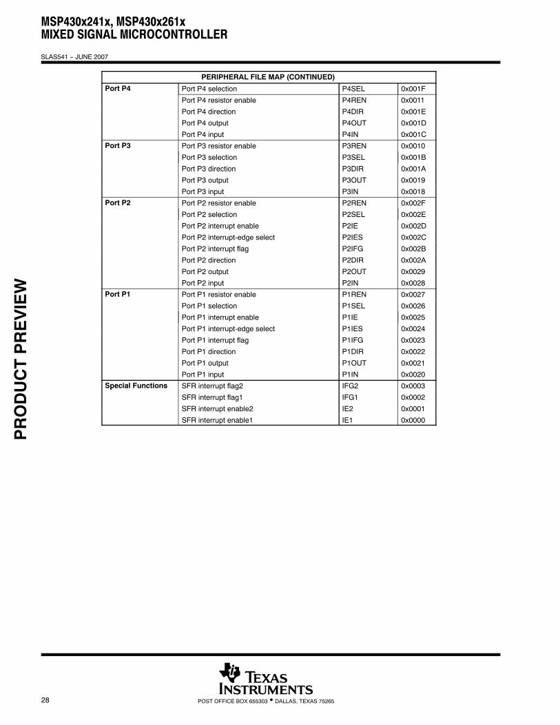
PERIPHERAL FILE MAP (CONTINUED)
Port P4 Port P4 selection P4SEL 0x001F
Port P4 resistor enable P4REN 0x0011
Port P4 direction P4DIR 0x001E
Port P4 output P4OUT 0x001D
Port P4 input P4IN 0x001C
Port P3 Port P3 resistor enable P3REN 0x0010
Port P3 selection P3SEL 0x001B
Port P3 direction P3DIR 0x001A
Port P3 output P3OUT 0x0019
Port P3 input P3IN 0x0018
Port P2 Port P2 resistor enable P2REN 0x002F
Port P2 selection P2SEL 0x002E
Port P2 interrupt enable P2IE 0x002D
Port P2 interrupt-edge select P2IES 0x002C
Port P2 interrupt flag P2IFG 0x002B
Port P2 direction P2DIR 0x002A
Port P2 output P2OUT 0x0029
Port P2 input P2IN 0x0028
Port P1 Port P1 resistor enable P1REN 0x0027
Port P1 selection P1SEL 0x0026
Port P1 interrupt enable P1IE 0x0025
Port P1 interrupt-edge select P1IES 0x0024
Port P1 interrupt flag P1IFG 0x0023
Port P1 direction P1DIR 0x0022
Port P1 output P1OUT 0x0021
Port P1 input P1IN 0x0020
Special Functions SFR interrupt flag2 IFG2 0x0003p
SFR interrupt flag1 IFG1 0x0002
SFR interrupt enable2 IE2 0x0001
SFR interrupt enable1 IE1 0x0000
PRODUCTPREVIEW
MSP430x241x, MSP430x261xMIXED SIGNAL MICROCONTROLLER
SLAS541 -- JUNE 2007
29POST OFFICE BOX 655303 • DALLAS, TEXAS 75265
Data Sheet Revision HistoryLiteratureNumber Summary
SLAS541 Initial Product Preview release
PRODUCTPREVIEW
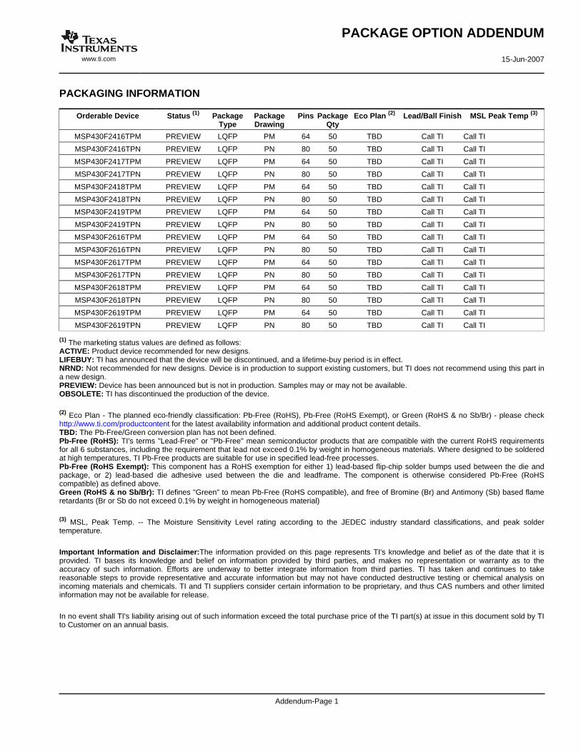
PACKAGING INFORMATION
Orderable Device Status (1) PackageType
PackageDrawing
Pins PackageQty
Eco Plan (2) Lead/Ball Finish MSL Peak Temp (3)
MSP430F2416TPM PREVIEW LQFP PM 64 50 TBD Call TI Call TI
MSP430F2416TPN PREVIEW LQFP PN 80 50 TBD Call TI Call TI
MSP430F2417TPM PREVIEW LQFP PM 64 50 TBD Call TI Call TI
MSP430F2417TPN PREVIEW LQFP PN 80 50 TBD Call TI Call TI
MSP430F2418TPM PREVIEW LQFP PM 64 50 TBD Call TI Call TI
MSP430F2418TPN PREVIEW LQFP PN 80 50 TBD Call TI Call TI
MSP430F2419TPM PREVIEW LQFP PM 64 50 TBD Call TI Call TI
MSP430F2419TPN PREVIEW LQFP PN 80 50 TBD Call TI Call TI
MSP430F2616TPM PREVIEW LQFP PM 64 50 TBD Call TI Call TI
MSP430F2616TPN PREVIEW LQFP PN 80 50 TBD Call TI Call TI
MSP430F2617TPM PREVIEW LQFP PM 64 50 TBD Call TI Call TI
MSP430F2617TPN PREVIEW LQFP PN 80 50 TBD Call TI Call TI
MSP430F2618TPM PREVIEW LQFP PM 64 50 TBD Call TI Call TI
MSP430F2618TPN PREVIEW LQFP PN 80 50 TBD Call TI Call TI
MSP430F2619TPM PREVIEW LQFP PM 64 50 TBD Call TI Call TI
MSP430F2619TPN PREVIEW LQFP PN 80 50 TBD Call TI Call TI
(1) The marketing status values are defined as follows:ACTIVE: Product device recommended for new designs.LIFEBUY: TI has announced that the device will be discontinued, and a lifetime-buy period is in effect.NRND: Not recommended for new designs. Device is in production to support existing customers, but TI does not recommend using this part ina new design.PREVIEW: Device has been announced but is not in production. Samples may or may not be available.OBSOLETE: TI has discontinued the production of the device.
(2) Eco Plan - The planned eco-friendly classification: Pb-Free (RoHS), Pb-Free (RoHS Exempt), or Green (RoHS & no Sb/Br) - please checkhttp://www.ti.com/productcontent for the latest availability information and additional product content details.TBD: The Pb-Free/Green conversion plan has not been defined.Pb-Free (RoHS): TI's terms "Lead-Free" or "Pb-Free" mean semiconductor products that are compatible with the current RoHS requirementsfor all 6 substances, including the requirement that lead not exceed 0.1% by weight in homogeneous materials. Where designed to be solderedat high temperatures, TI Pb-Free products are suitable for use in specified lead-free processes.Pb-Free (RoHS Exempt): This component has a RoHS exemption for either 1) lead-based flip-chip solder bumps used between the die andpackage, or 2) lead-based die adhesive used between the die and leadframe. The component is otherwise considered Pb-Free (RoHScompatible) as defined above.Green (RoHS & no Sb/Br): TI defines "Green" to mean Pb-Free (RoHS compatible), and free of Bromine (Br) and Antimony (Sb) based flameretardants (Br or Sb do not exceed 0.1% by weight in homogeneous material)
(3) MSL, Peak Temp. -- The Moisture Sensitivity Level rating according to the JEDEC industry standard classifications, and peak soldertemperature.
Important Information and Disclaimer:The information provided on this page represents TI's knowledge and belief as of the date that it isprovided. TI bases its knowledge and belief on information provided by third parties, and makes no representation or warranty as to theaccuracy of such information. Efforts are underway to better integrate information from third parties. TI has taken and continues to takereasonable steps to provide representative and accurate information but may not have conducted destructive testing or chemical analysis onincoming materials and chemicals. TI and TI suppliers consider certain information to be proprietary, and thus CAS numbers and other limitedinformation may not be available for release.
In no event shall TI's liability arising out of such information exceed the total purchase price of the TI part(s) at issue in this document sold by TIto Customer on an annual basis.
PACKAGE OPTION ADDENDUM
www.ti.com 15-Jun-2007
Addendum-Page 1
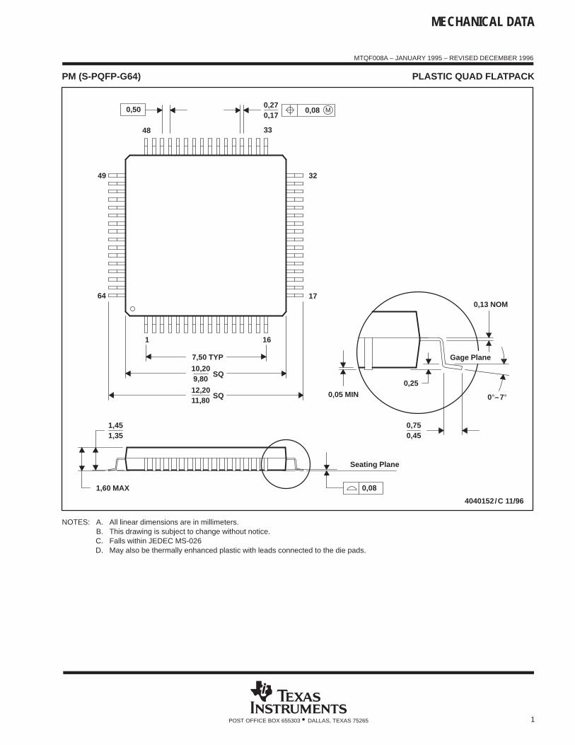
MECHANICAL DATA
MTQF008A – JANUARY 1995 – REVISED DECEMBER 1996
1POST OFFICE BOX 655303 • DALLAS, TEXAS 75265
PM (S-PQFP-G64) PLASTIC QUAD FLATPACK
4040152/C 11/96
32
170,13 NOM
0,25
0,450,75
Seating Plane
0,05 MIN
Gage Plane
0,27
33
16
48
1
0,17
49
64
SQ
SQ10,20
11,8012,20
9,80
7,50 TYP
1,60 MAX
1,451,35
0,08
0,50 M0,08
0°–7°
NOTES: A. All linear dimensions are in millimeters.B. This drawing is subject to change without notice.C. Falls within JEDEC MS-026D. May also be thermally enhanced plastic with leads connected to the die pads.
MECHANICAL DATA
MTQF010A – JANUARY 1995 – REVISED DECEMBER 1996
1POST OFFICE BOX 655303 • DALLAS, TEXAS 75265
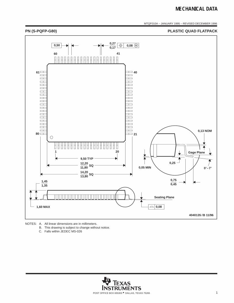
PN (S-PQFP-G80) PLASTIC QUAD FLATPACK
4040135 /B 11/96
0,170,27
0,13 NOM
40
21
0,25
0,450,75
0,05 MIN
Seating Plane
Gage Plane
4160
61
80
20
SQ
SQ
1
13,8014,20
12,20
9,50 TYP
11,80
1,451,35
1,60 MAX 0,08
0,50 M0,08
0°–7°
NOTES: A. All linear dimensions are in millimeters.B. This drawing is subject to change without notice.C. Falls within JEDEC MS-026
IMPORTANT NOTICE
Texas Instruments Incorporated and its subsidiaries (TI) reserve the right to make corrections, modifications, enhancements,improvements, and other changes to its products and services at any time and to discontinue any product or service without notice.Customers should obtain the latest relevant information before placing orders and should verify that such information is current andcomplete. All products are sold subject to TI’s terms and conditions of sale supplied at the time of order acknowledgment.
TI warrants performance of its hardware products to the specifications applicable at the time of sale in accordance with TI’sstandard warranty. Testing and other quality control techniques are used to the extent TI deems necessary to support thiswarranty. Except where mandated by government requirements, testing of all parameters of each product is not necessarilyperformed.
TI assumes no liability for applications assistance or customer product design. Customers are responsible for their products andapplications using TI components. To minimize the risks associated with customer products and applications, customers shouldprovide adequate design and operating safeguards.
TI does not warrant or represent that any license, either express or implied, is granted under any TI patent right, copyright, maskwork right, or other TI intellectual property right relating to any combination, machine, or process in which TI products or servicesare used. Information published by TI regarding third-party products or services does not constitute a license from TI to use suchproducts or services or a warranty or endorsement thereof. Use of such information may require a license from a third party underthe patents or other intellectual property of the third party, or a license from TI under the patents or other intellectual property of TI.
Reproduction of TI information in TI data books or data sheets is permissible only if reproduction is without alteration and isaccompanied by all associated warranties, conditions, limitations, and notices. Reproduction of this information with alteration is anunfair and deceptive business practice. TI is not responsible or liable for such altered documentation. Information of third partiesmay be subject to additional restrictions.
Resale of TI products or services with statements different from or beyond the parameters stated by TI for that product or servicevoids all express and any implied warranties for the associated TI product or service and is an unfair and deceptive businesspractice. TI is not responsible or liable for any such statements.
TI products are not authorized for use in safety-critical applications (such as life support) where a failure of the TI product wouldreasonably be expected to cause severe personal injury or death, unless officers of the parties have executed an agreementspecifically governing such use. Buyers represent that they have all necessary expertise in the safety and regulatory ramificationsof their applications, and acknowledge and agree that they are solely responsible for all legal, regulatory and safety-relatedrequirements concerning their products and any use of TI products in such safety-critical applications, notwithstanding anyapplications-related information or support that may be provided by TI. Further, Buyers must fully indemnify TI and itsrepresentatives against any damages arising out of the use of TI products in such safety-critical applications.
TI products are neither designed nor intended for use in military/aerospace applications or environments unless the TI products arespecifically designated by TI as military-grade or "enhanced plastic." Only products designated by TI as military-grade meet militaryspecifications. Buyers acknowledge and agree that any such use of TI products which TI has not designated as military-grade issolely at the Buyer's risk, and that they are solely responsible for compliance with all legal and regulatory requirements inconnection with such use.
TI products are neither designed nor intended for use in automotive applications or environments unless the specific TI productsare designated by TI as compliant with ISO/TS 16949 requirements. Buyers acknowledge and agree that, if they use anynon-designated products in automotive applications, TI will not be responsible for any failure to meet such requirements.
Following are URLs where you can obtain information on other Texas Instruments products and application solutions:
Products Applications
Amplifiers amplifier.ti.com Audio www.ti.com/audio
Data Converters dataconverter.ti.com Automotive www.ti.com/automotive
DSP dsp.ti.com Broadband www.ti.com/broadband
Interface interface.ti.com Digital Control www.ti.com/digitalcontrol
Logic logic.ti.com Military www.ti.com/military
Power Mgmt power.ti.com Optical Networking www.ti.com/opticalnetwork
Microcontrollers microcontroller.ti.com Security www.ti.com/security
RFID www.ti-rfid.com Telephony www.ti.com/telephony
Low Power www.ti.com/lpw Video & Imaging www.ti.com/videoWireless
Wireless www.ti.com/wireless
Mailing Address: Texas Instruments, Post Office Box 655303, Dallas, Texas 75265Copyright © 2007, Texas Instruments Incorporated

![Plastic Film Capacitors - Panasonic · Insulation resistance (IR) Withstand voltage ±10 % (K), ±20 % (M) Category temp. range −40 ℃ to +110 ℃ Rated voltage [AC] 275 V Capacitance](https://static.fdocument.org/doc/165x107/5eaa86acb8948405283e9700/plastic-film-capacitors-panasonic-insulation-resistance-ir-withstand-voltage.jpg)