20 W bridge/stereo amplifier for car radio · January 2010 Doc ID 1451 Rev 4 1/25 1 TDA2005 20 W...
25
January 2010 Doc ID 1451 Rev 4 1/25 1 TDA2005 20 W bridge/stereo amplifier for car radio Features ■ High output power: – P o = 10 + 10 W @ R L = 2 Ω, THD = 10 % – P o = 20 W @ R L = 4 Ω , THD = 10 %. ■ Protection against: – Output DC and AC short circuit to ground – Overrating chip temperature – Load dump voltage surge – Fortuitous open ground – Very inductive loads ■ Loudspeaker protection during short circuit for one wire to ground Description The TDA2005 is a class B dual audio power amplifier in Multiwatt11 package specifically designed for car radio applications. Power booster amplifiers can be easily designed using this device that provides a high current capability (up to 3.5 A) and can drive very low impedance loads (down to 1.6 Ω in stereo applications) obtaining an output power of more than 20 W (bridge configuration). Multiwatt11 Table 1. Device summary Order code Package Packing TDA2005R Multiwatt11 Tube TDA2005M (1) 1. Do not use for New Design. Multiwatt11 Tube TDA2005S (1) Multiwatt11 Tube www.st.com
Transcript of 20 W bridge/stereo amplifier for car radio · January 2010 Doc ID 1451 Rev 4 1/25 1 TDA2005 20 W...
January 2010 Doc ID 1451 Rev 4 1/25
1
TDA2005
20 W bridge/stereo amplifier for car radio
Features■ High output power:
– Po = 10 + 10 W @ RL = 2 Ω, THD = 10 % – Po = 20 W @ RL = 4 Ω , THD = 10 %.
■ Protection against: – Output DC and AC short circuit to ground – Overrating chip temperature – Load dump voltage surge– Fortuitous open ground– Very inductive loads
■ Loudspeaker protection during short circuit for one wire to ground
DescriptionThe TDA2005 is a class B dual audio power amplifier in Multiwatt11 package specifically designed for car radio applications.
Power booster amplifiers can be easily designed using this device that provides a high current capability (up to 3.5 A) and can drive very low impedance loads (down to 1.6 Ω in stereo applications) obtaining an output power of more than 20 W (bridge configuration).
Multiwatt11
Table 1. Device summary
Order code Package Packing
TDA2005R Multiwatt11 Tube
TDA2005M(1)
1. Do not use for New Design.
Multiwatt11 Tube
TDA2005S(1) Multiwatt11 Tube
www.st.com
Contents TDA2005
2/25 Doc ID 1451 Rev 4
Contents
1 Schematic and pins connection diagrams . . . . . . . . . . . . . . . . . . . . . . . 5
2 Electrical specifications . . . . . . . . . . . . . . . . . . . . . . . . . . . . . . . . . . . . . . 6
2.1 Absolute maximum ratings . . . . . . . . . . . . . . . . . . . . . . . . . . . . . . . . . . . . . 6
2.2 Thermal data . . . . . . . . . . . . . . . . . . . . . . . . . . . . . . . . . . . . . . . . . . . . . . . 6
2.3 Bridge amplifier section . . . . . . . . . . . . . . . . . . . . . . . . . . . . . . . . . . . . . . . 6
2.3.1 Electrical characteristics (bridge application) . . . . . . . . . . . . . . . . . . . . . . 7
2.3.2 Bridge amplifier design . . . . . . . . . . . . . . . . . . . . . . . . . . . . . . . . . . . . . . 9
2.4 Stereo amplifier application . . . . . . . . . . . . . . . . . . . . . . . . . . . . . . . . . . . 10
2.4.1 Electrical characteristics (stereo application) . . . . . . . . . . . . . . . . . . . . . 11
3 Application suggestion . . . . . . . . . . . . . . . . . . . . . . . . . . . . . . . . . . . . . . 15
4 Application information . . . . . . . . . . . . . . . . . . . . . . . . . . . . . . . . . . . . . 16
4.1 Built-in protection systems . . . . . . . . . . . . . . . . . . . . . . . . . . . . . . . . . . . . 20
4.1.1 Load dump voltage surge . . . . . . . . . . . . . . . . . . . . . . . . . . . . . . . . . . . 20
4.1.2 Short circuit (AC and DC conditions) . . . . . . . . . . . . . . . . . . . . . . . . . . . 21
4.1.3 Polarity inversion . . . . . . . . . . . . . . . . . . . . . . . . . . . . . . . . . . . . . . . . . . 21
4.1.4 Open ground . . . . . . . . . . . . . . . . . . . . . . . . . . . . . . . . . . . . . . . . . . . . . 21
4.1.5 Inductive load . . . . . . . . . . . . . . . . . . . . . . . . . . . . . . . . . . . . . . . . . . . . . 21
4.1.6 DC voltage . . . . . . . . . . . . . . . . . . . . . . . . . . . . . . . . . . . . . . . . . . . . . . . 21
4.1.7 Thermal shut-down . . . . . . . . . . . . . . . . . . . . . . . . . . . . . . . . . . . . . . . . 22
4.1.8 Loudspeaker protection . . . . . . . . . . . . . . . . . . . . . . . . . . . . . . . . . . . . . 22
5 Package information . . . . . . . . . . . . . . . . . . . . . . . . . . . . . . . . . . . . . . . . 23
6 Revision history . . . . . . . . . . . . . . . . . . . . . . . . . . . . . . . . . . . . . . . . . . . 24

TDA2005 List of tables
Doc ID 1451 Rev 4 3/25
List of tables
Table 1. Device summary . . . . . . . . . . . . . . . . . . . . . . . . . . . . . . . . . . . . . . . . . . . . . . . . . . . . . . . . . . 1Table 2. Absolute maximum ratings . . . . . . . . . . . . . . . . . . . . . . . . . . . . . . . . . . . . . . . . . . . . . . . . . . 6Table 3. Thermal data. . . . . . . . . . . . . . . . . . . . . . . . . . . . . . . . . . . . . . . . . . . . . . . . . . . . . . . . . . . . . 6Table 4. Electrical characteristics (bridge application) . . . . . . . . . . . . . . . . . . . . . . . . . . . . . . . . . . . . 7Table 5. Bridge amplifier design . . . . . . . . . . . . . . . . . . . . . . . . . . . . . . . . . . . . . . . . . . . . . . . . . . . . . 9Table 6. High gain vs. Rx . . . . . . . . . . . . . . . . . . . . . . . . . . . . . . . . . . . . . . . . . . . . . . . . . . . . . . . . . 10Table 7. Electrical characteristics (stereo application) . . . . . . . . . . . . . . . . . . . . . . . . . . . . . . . . . . . 11Table 8. Recommended values of the component of the bridge application circuit . . . . . . . . . . . . . 15Table 9. Document revision history . . . . . . . . . . . . . . . . . . . . . . . . . . . . . . . . . . . . . . . . . . . . . . . . . 24
List of figures TDA2005
4/25 Doc ID 1451 Rev 4
List of figures
Figure 1. Schematic diagram . . . . . . . . . . . . . . . . . . . . . . . . . . . . . . . . . . . . . . . . . . . . . . . . . . . . . . . . 5Figure 2. Pins connection diagram (top view) . . . . . . . . . . . . . . . . . . . . . . . . . . . . . . . . . . . . . . . . . . . 5Figure 3. Test and application circuit (bridge amplifier) . . . . . . . . . . . . . . . . . . . . . . . . . . . . . . . . . . . . 6Figure 4. PC board and components layout of Figure 3 . . . . . . . . . . . . . . . . . . . . . . . . . . . . . . . . . . . 7Figure 5. Output offset voltage vs. supply voltage . . . . . . . . . . . . . . . . . . . . . . . . . . . . . . . . . . . . . . . . 8Figure 6. Distortion vs. output power (RL = 4 Ω) . . . . . . . . . . . . . . . . . . . . . . . . . . . . . . . . . . . . . . . . . 8Figure 7. Distortion vs. output power (RL = 3.2 Ω) . . . . . . . . . . . . . . . . . . . . . . . . . . . . . . . . . . . . . . . . 8Figure 8. Bridge configuration . . . . . . . . . . . . . . . . . . . . . . . . . . . . . . . . . . . . . . . . . . . . . . . . . . . . . . 10Figure 9. Typical stereo application circuit . . . . . . . . . . . . . . . . . . . . . . . . . . . . . . . . . . . . . . . . . . . . . 10Figure 10. Quiescent output voltage vs. supply voltage (stereo amplifier). . . . . . . . . . . . . . . . . . . . . . 12Figure 11. Quiescent drain current vs. supply voltage (stereo amplifier) . . . . . . . . . . . . . . . . . . . . . . . 12Figure 12. Distortion vs. output power (stereo amplifier) . . . . . . . . . . . . . . . . . . . . . . . . . . . . . . . . . . . 12Figure 13. Output power vs. supply voltage, RL = 2 and 4 Ω (stereo amplifier). . . . . . . . . . . . . . . . . . 12Figure 14. Output power vs. supply voltage, RL = 1.6 and 3.2Ω (Stereo amplifier) . . . . . . . . . . . . . . . 13Figure 15. Distortion vs. frequency, RL = 2 and 4 Ω (stereo amplifier) . . . . . . . . . . . . . . . . . . . . . . . . 13Figure 16. Distortion vs. frequency, RL = 1.6 and 3.2 Ω (stereo amplifier) . . . . . . . . . . . . . . . . . . . . . 13Figure 17. Supply voltage rejection vs. C3 (stereo amplifier). . . . . . . . . . . . . . . . . . . . . . . . . . . . . . . . 13Figure 18. Supply voltage rejection vs. frequency (stereo amplifier) . . . . . . . . . . . . . . . . . . . . . . . . . . 13Figure 19. Supply voltage rejection vs. C2 and C3, GV = 390/1Ω (stereo amplifier) . . . . . . . . . . . . . . 13Figure 20. Supply voltage rejection vs. C2 and C3, GV = 1000/10Ω (stereo amplifier) . . . . . . . . . . . . 14Figure 21. Gain vs. input sensitivity RL = 4 Ω (stereo amplifier) . . . . . . . . . . . . . . . . . . . . . . . . . . . . . 14Figure 22. Gain vs. input sensitivity RL = 2 Ω (stereo amplifier) . . . . . . . . . . . . . . . . . . . . . . . . . . . . . 14Figure 23. Total power dissipation and efficiency vs. output power (bridge) . . . . . . . . . . . . . . . . . . . . 14Figure 24. Total power dissipation and efficiency vs. output power (stereo) . . . . . . . . . . . . . . . . . . . . 14Figure 25. Bridge amplifier without boostrap . . . . . . . . . . . . . . . . . . . . . . . . . . . . . . . . . . . . . . . . . . . . 16Figure 26. PC board and components layout of Figure 25 . . . . . . . . . . . . . . . . . . . . . . . . . . . . . . . . . 16Figure 27. Low cost bridge amplifier (GV = 42dB) . . . . . . . . . . . . . . . . . . . . . . . . . . . . . . . . . . . . . . . . 17Figure 28. PC board and components layout of Figure 27 . . . . . . . . . . . . . . . . . . . . . . . . . . . . . . . . . 17Figure 29. 10 + 10 W stereo amplifier with tone balance and loudness control. . . . . . . . . . . . . . . . . . 18Figure 30. Tone control response (circuit of Figure 29) . . . . . . . . . . . . . . . . . . . . . . . . . . . . . . . . . . . . 18Figure 31. 20 W bus amplifier . . . . . . . . . . . . . . . . . . . . . . . . . . . . . . . . . . . . . . . . . . . . . . . . . . . . . . . 19Figure 32. Simple 20 W two way amplifier (FC = 2 kHz) . . . . . . . . . . . . . . . . . . . . . . . . . . . . . . . . . . . 19Figure 33. Bridge amplifier circuit suited for low-gain applications (GV = 34 dB) . . . . . . . . . . . . . . . . 20Figure 34. Example of muting circuit . . . . . . . . . . . . . . . . . . . . . . . . . . . . . . . . . . . . . . . . . . . . . . . . . . 20Figure 35. Suggested LC network circuit . . . . . . . . . . . . . . . . . . . . . . . . . . . . . . . . . . . . . . . . . . . . . . . 21Figure 36. Voltage gain bridge configuration . . . . . . . . . . . . . . . . . . . . . . . . . . . . . . . . . . . . . . . . . . . . 21Figure 37. Maximum allowable power dissipation vs. ambient temperature . . . . . . . . . . . . . . . . . . . . 22Figure 38. Output power and drain current vs. case temperature (RL = 4 Ω) . . . . . . . . . . . . . . . . . . . 22Figure 39. Output power and drain current vs. case temperature (RL = 3.2 Ω) . . . . . . . . . . . . . . . . . . 22Figure 40. Multiwatt11 mechanical data and package dimensions . . . . . . . . . . . . . . . . . . . . . . . . . . . 23
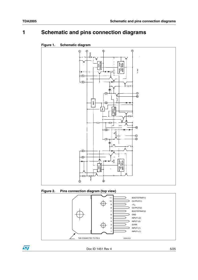
TDA2005 Schematic and pins connection diagrams
Doc ID 1451 Rev 4 5/25
1 Schematic and pins connection diagrams
Figure 1. Schematic diagram
Figure 2. Pins connection diagram (top view)
1
2
3
4
5
6
7
9
10
11
8
BOOTSTRAP(1)
INPUT-(1)
SVRR
GND
INPUT-(2)
INPUT+(2)
OUTPUT(2)
+VS
OUTPUT(1)
INPUT+(1)
TAB CONNECTED TO PIN 6 D95AU318
BOOTSTRAP(2)
Electrical specifications TDA2005
6/25 Doc ID 1451 Rev 4
2 Electrical specifications
2.1 Absolute maximum ratings
2.2 Thermal data
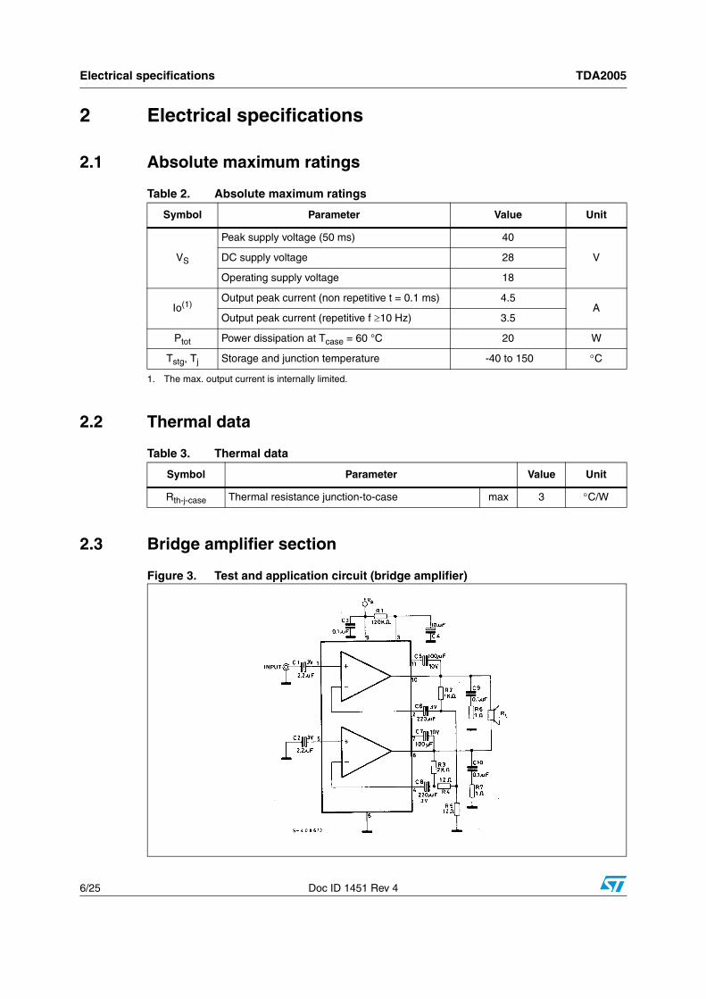
2.3 Bridge amplifier section
Figure 3. Test and application circuit (bridge amplifier)
Table 2. Absolute maximum ratings
Symbol Parameter Value Unit
VS
Peak supply voltage (50 ms) 40
VDC supply voltage 28
Operating supply voltage 18
Io(1)
1. The max. output current is internally limited.
Output peak current (non repetitive t = 0.1 ms) 4.5A
Output peak current (repetitive f ≥10 Hz) 3.5
Ptot Power dissipation at Tcase = 60 °C 20 W
Tstg, Tj Storage and junction temperature -40 to 150 °C
Table 3. Thermal data
Symbol Parameter Value Unit
Rth-j-case Thermal resistance junction-to-case max 3 °C/W
TDA2005 Electrical specifications
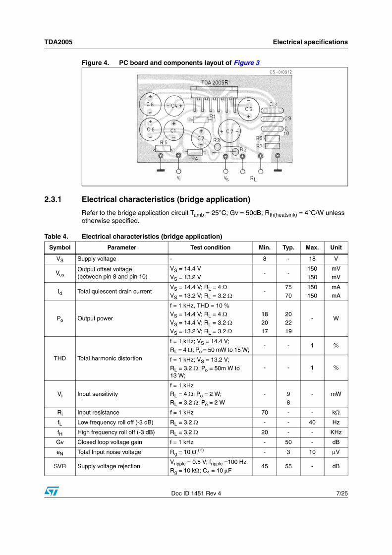
Doc ID 1451 Rev 4 7/25
Figure 4. PC board and components layout of Figure 3
2.3.1 Electrical characteristics (bridge application)
Refer to the bridge application circuit Tamb = 25°C; Gv = 50dB; Rth(heatsink) = 4°C/W unless otherwise specified.
Table 4. Electrical characteristics (bridge application)
Symbol Parameter Test condition Min. Typ. Max. Unit
VS Supply voltage - 8 - 18 V
VosOutput offset voltage (between pin 8 and pin 10)
VS = 14.4 VVS = 13.2 V
- -150150
mVmV
Id Total quiescent drain current VS = 14.4 V; RL = 4 ΩVS = 13.2 V; RL = 3.2 Ω
-75
70
150
150
mA
mA
Po Output power
f = 1 kHz, THD = 10 %
VS = 14.4 V; RL = 4 ΩVS = 14.4 V; RL = 3.2 ΩVS = 13.2 V; RL = 3.2 Ω
1820
17
2022
19
- W
THD Total harmonic distortion
f = 1 kHz; VS = 14.4 V;
RL = 4 Ω; Po = 50 mW to 15 W; - - 1 %
f = 1 kHz; VS = 13.2 V;RL = 3.2 Ω; Po = 50m W to 13 W;
- - 1 %
Vi Input sensitivityf = 1 kHzRL = 4 Ω; Po = 2 W;
RL = 3.2 Ω; Po = 2 W
- 9
8
- mW
Ri Input resistance f = 1 kHz 70 - - kΩ
fL Low frequency roll off (-3 dB) RL = 3.2 Ω - - 40 Hz
fH High frequency roll off (-3 dB) RL = 3.2 Ω 20 - - KHz
Gv Closed loop voltage gain f = 1 kHz - 50 - dB
eN Total Input noise voltage Rg = 10 Ω (1) - 3 10 μV
SVR Supply voltage rejectionVripple = 0.5 V; fripple =100 Hz
Rg = 10 kΩ; C4 = 10 μF45 55 - dB

Electrical specifications TDA2005
8/25 Doc ID 1451 Rev 4
η Efficiency
f = 1 kHz; VS = 14.4 V;
RL = 4 Ω; Po = 20 W;
RL = 3.2 Ω; Po = 22 W
- 60
60
-
%
f = 1 kHz; VS = 13.2 V;RL = 3.2 Ω; Po = 19 W
- 58 -
SVR Supply voltage rejection f = 100 Hz; Vripple = 0.5 V;
Rg = 10 kΩ; RL = 4 Ω30 36 - dB
TjThermal shut-down junction temperature
f = 1 kHz; VS = 14.4V;
RL = 4 Ω; Ptot = 13 W- 145 - °C
VOSHOutput voltage with one side of the speaker shorted to ground
VS = 14.4 V; RL = 4 ΩVS = 13.2 V; RL = 3.2 Ω
- - 2 V
1. Bandwidth filter: 22 Hz to 22 kHz.
Figure 5. Output offset voltage vs. supply voltage
Figure 6. Distortion vs. output power (RL = 4 Ω)
Figure 7. Distortion vs. output power (RL = 3.2 Ω)
Table 4. Electrical characteristics (bridge application) (continued)
Symbol Parameter Test condition Min. Typ. Max. Unit
Vos(mV)
Vs (V)
100
80
60
40
20
0
8 10 12 14 16
Vs = 14.4 VGv = 50 dBRL = 4 Ωf = 1 kHz
d(%)
1
1 10
0.1
10
Po (W)
Vs = 13.2 VGv = 50 dBRL = 3.2 Ωf = 1 kHz
d(%)
1
1 10
0.1
10
Po (W)
TDA2005 Electrical specifications
Doc ID 1451 Rev 4 9/25
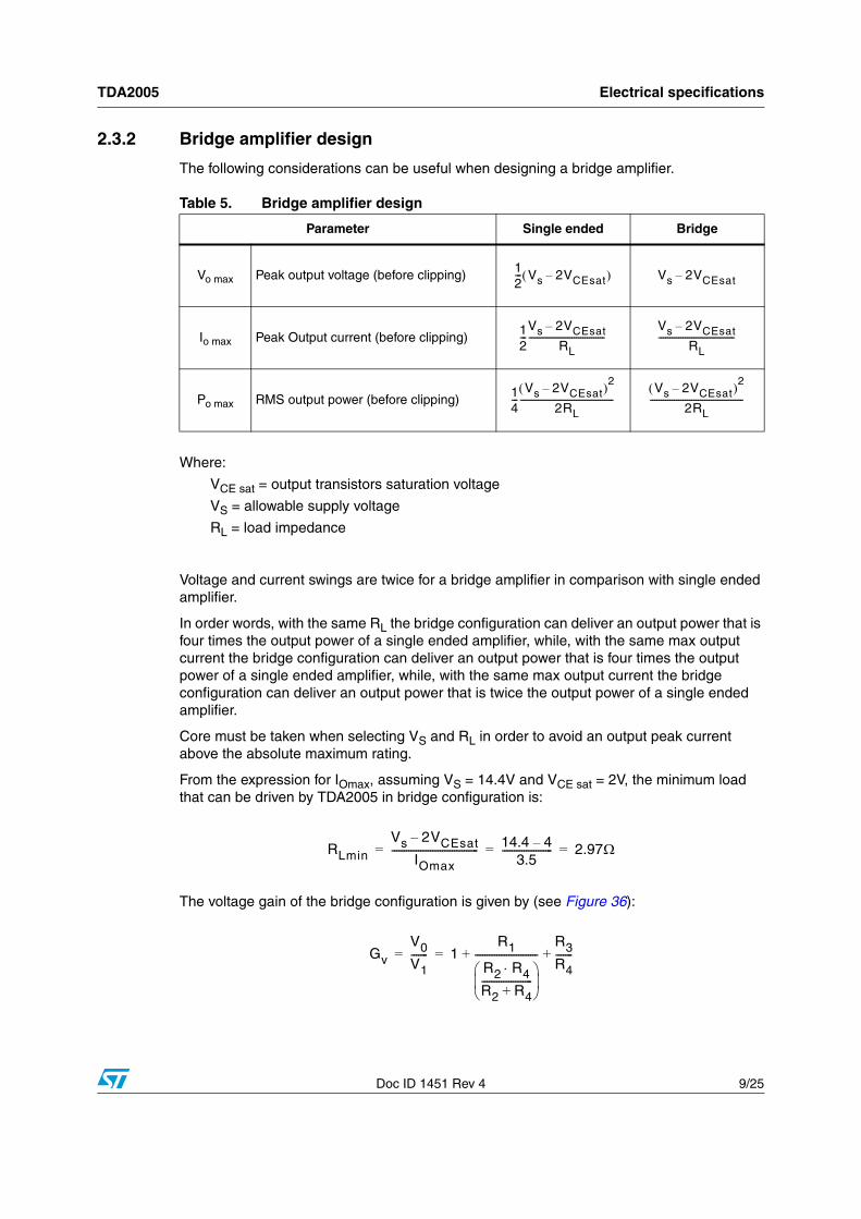
2.3.2 Bridge amplifier design
The following considerations can be useful when designing a bridge amplifier.
Where:
VCE sat = output transistors saturation voltage
VS = allowable supply voltage
RL = load impedance
Voltage and current swings are twice for a bridge amplifier in comparison with single ended amplifier.
In order words, with the same RL the bridge configuration can deliver an output power that is four times the output power of a single ended amplifier, while, with the same max output current the bridge configuration can deliver an output power that is four times the output power of a single ended amplifier, while, with the same max output current the bridge configuration can deliver an output power that is twice the output power of a single ended amplifier.
Core must be taken when selecting VS and RL in order to avoid an output peak current above the absolute maximum rating.
From the expression for IOmax, assuming VS = 14.4V and VCE sat = 2V, the minimum load that can be driven by TDA2005 in bridge configuration is:
The voltage gain of the bridge configuration is given by (see Figure 36):
Table 5. Bridge amplifier design
Parameter Single ended Bridge
Vo max Peak output voltage (before clipping)
Io max Peak Output current (before clipping)
Po max RMS output power (before clipping)
12--- Vs 2VCEsat–( ) Vs 2VCEsat–
12---
Vs 2VCEsat–RL
-----------------------------------Vs 2VCEsat–
RL-----------------------------------
14---
Vs 2VCEsat–( )2
2RL-------------------------------------------
Vs 2VCEsat–( )2
2RL-------------------------------------------
RLmin
Vs 2VCEsat–IOmax
------------------------------------ 14.4 4–3.5
--------------------- 2.97Ω= = =
Gv
V0V1------- 1
R1
R2 R4⋅
R2 R4+---------------------
⎝ ⎠⎜ ⎟⎛ ⎞--------------------------
R3R4-------+ += =
Electrical specifications TDA2005
10/25 Doc ID 1451 Rev 4
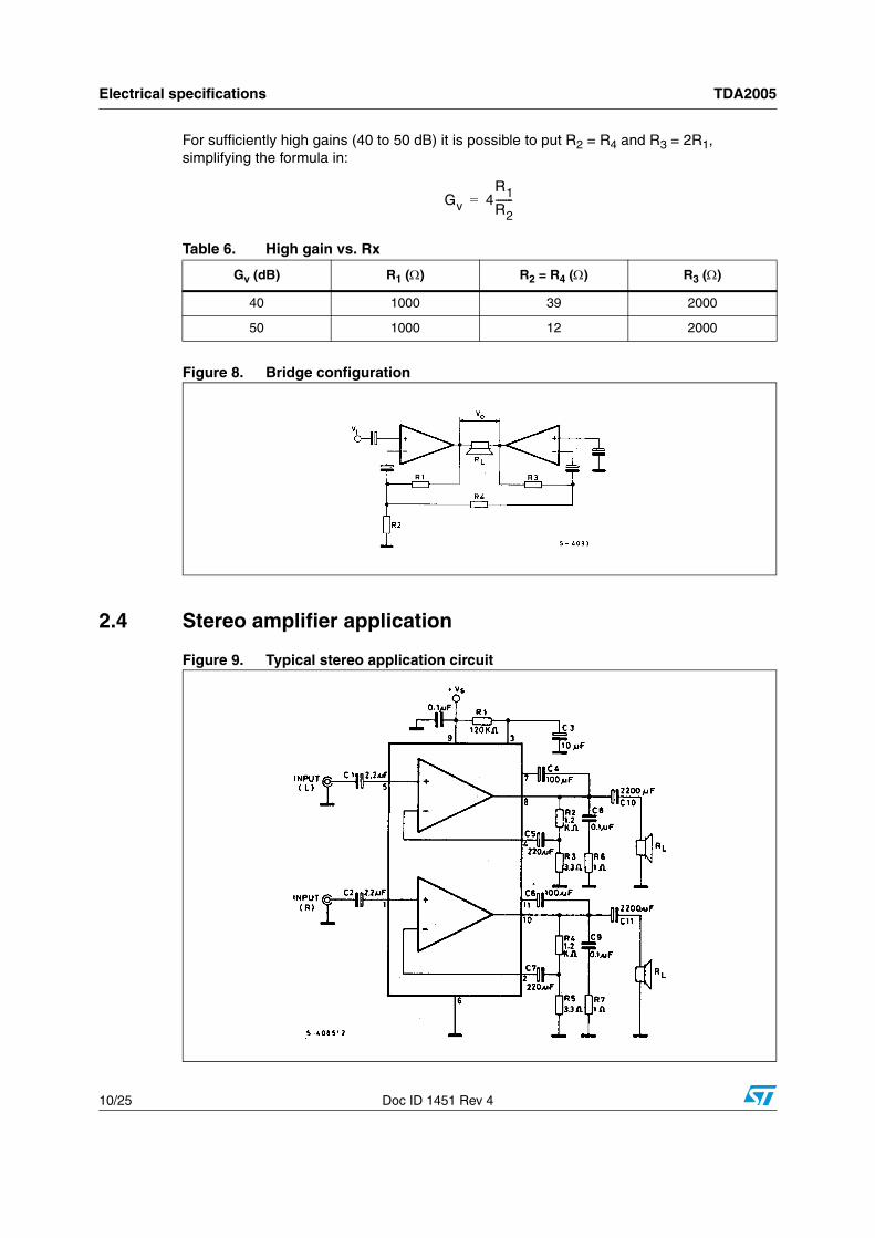
For sufficiently high gains (40 to 50 dB) it is possible to put R2 = R4 and R3 = 2R1, simplifying the formula in:
Figure 8. Bridge configuration
2.4 Stereo amplifier application
Figure 9. Typical stereo application circuit
Table 6. High gain vs. Rx
Gv (dB) R1 (Ω) R2 = R4 (Ω) R3 (Ω)
40 1000 39 2000
50 1000 12 2000
Gv 4R1R2-------=
TDA2005 Electrical specifications
Doc ID 1451 Rev 4 11/25
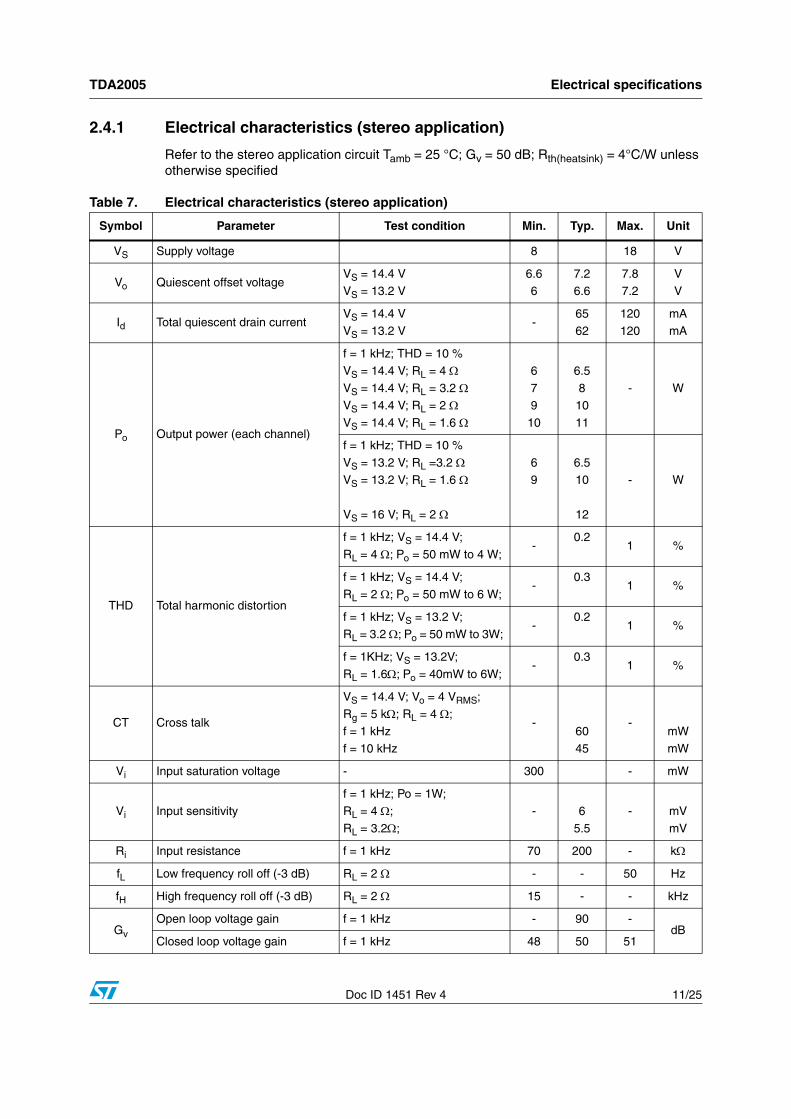
2.4.1 Electrical characteristics (stereo application)
Refer to the stereo application circuit Tamb = 25 °C; Gv = 50 dB; Rth(heatsink) = 4°C/W unless otherwise specified
Table 7. Electrical characteristics (stereo application)
Symbol Parameter Test condition Min. Typ. Max. Unit
VS Supply voltage 8 18 V
Vo Quiescent offset voltage VS = 14.4 VVS = 13.2 V
6.66
7.26.6
7.87.2
VV
Id Total quiescent drain current VS = 14.4 V VS = 13.2 V
-6562
120120
mAmA
Po Output power (each channel)
f = 1 kHz; THD = 10 %VS = 14.4 V; RL = 4 ΩVS = 14.4 V; RL = 3.2 ΩVS = 14.4 V; RL = 2 ΩVS = 14.4 V; RL = 1.6 Ω
6
7
9
10
6.5
8
10
11
- W
f = 1 kHz; THD = 10 %
VS = 13.2 V; RL =3.2 ΩVS = 13.2 V; RL = 1.6 Ω
VS = 16 V; RL = 2 Ω
69
6.510
12
- W
THD Total harmonic distortion
f = 1 kHz; VS = 14.4 V;
RL = 4 Ω; Po = 50 mW to 4 W; -
0.21 %
f = 1 kHz; VS = 14.4 V;
RL = 2 Ω; Po = 50 mW to 6 W; -
0.31 %
f = 1 kHz; VS = 13.2 V;
RL = 3.2 Ω; Po = 50 mW to 3W; -
0.21 %
f = 1KHz; VS = 13.2V;
RL = 1.6Ω; Po = 40mW to 6W; -
0.31 %
CT Cross talk
VS = 14.4 V; Vo = 4 VRMS;
Rg = 5 kΩ; RL = 4 Ω;f = 1 kHz
f = 10 kHz
-60
45
-mW
mW
Vi Input saturation voltage - 300 - mW
Vi Input sensitivityf = 1 kHz; Po = 1W; RL = 4 Ω; RL = 3.2Ω;
- 6
5.5
- mV
mV
Ri Input resistance f = 1 kHz 70 200 - kΩ
fL Low frequency roll off (-3 dB) RL = 2 Ω - - 50 Hz
fH High frequency roll off (-3 dB) RL = 2 Ω 15 - - kHz
Gv
Open loop voltage gain f = 1 kHz - 90 -dB
Closed loop voltage gain f = 1 kHz 48 50 51
Electrical specifications TDA2005
12/25 Doc ID 1451 Rev 4
ΔGv Closed loop gain matching - - 0.5 - dB
eN Total input noise voltage Rg = 10 kΩ(1) - 1.5 5 μV
SVR Supply voltage rejectionVripple = 0.5 V; fripple =100 Hz
Rg = 10 kΩ; C3 = 10 μF;35 45 - dB
η Efficiency
f = 1 kHz; VS = 14.4 V;
RL = 4 Ω; Po = 6.5 W; RL = 2Ω; Po = 10 W;
- 7060
- %
f = 1 kHz; VS = 13.2 V;RL = 3.2 Ω; Po = 6.5 W;
RL = 1.6 Ω; Po = 100 W;
- 70
60
- %
1. Bandwidth filter: 22 Hz to 22 kHz.
Figure 10. Quiescent output voltage vs. sup-ply voltage (stereo amplifier)
Figure 11. Quiescent drain current vs. supply voltage (stereo amplifier)
Figure 12. Distortion vs. output power (stereo amplifier)
Figure 13. Output power vs. supply voltage, RL = 2 and 4 Ω (stereo amplifier)
Table 7. Electrical characteristics (stereo application) (continued)
Symbol Parameter Test condition Min. Typ. Max. Unit
VO(V)
8
5
6
7
4
10 12 14 16 Vs (V)0 8
Id(mA)
100
80
60
40
20
10 12 14 16 Vs (V)0 8
d(%)
2
4
6
8
0
0.01 0.1 1 Po (W)
f = 1 kHzGv = 50 dB
Vs = 13.2 V RL = 1.6 Ω
Vs = 14.4 V RL = 2 Ω
Vs = 13.2 V RL = 3.2 Ω
Vs = 14.4 V RL = 4 Ω
Vs (V)
Po(W)
15
12
9
6
3
0
8 10 12 14 16
f = 1 kHzGv = 50 dBd = 10 %
RL = 2 Ω
RL = 4 Ω
TDA2005 Electrical specifications
Doc ID 1451 Rev 4 13/25
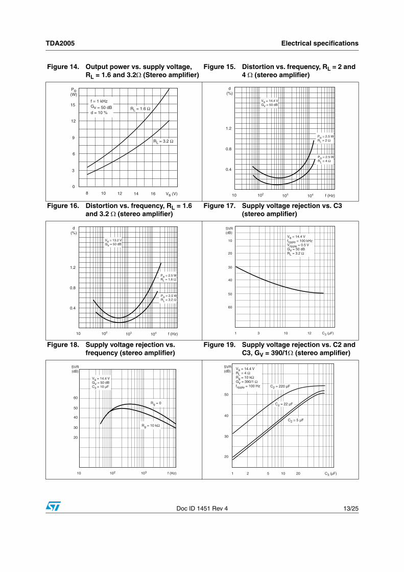
Figure 14. Output power vs. supply voltage, RL = 1.6 and 3.2Ω (Stereo amplifier)
Figure 15. Distortion vs. frequency, RL = 2 and 4 Ω (stereo amplifier)
Figure 16. Distortion vs. frequency, RL = 1.6 and 3.2 Ω (stereo amplifier)
Figure 17. Supply voltage rejection vs. C3 (stereo amplifier)
Figure 18. Supply voltage rejection vs. frequency (stereo amplifier)
Figure 19. Supply voltage rejection vs. C2 and C3, GV = 390/1Ω (stereo amplifier)
Vs (V)
Po(W)
15
12
9
6
3
0
8 10 12 14 16
f = 1 kHzGv = 50 dBd = 10 %
RL = 1.6 Ω
RL = 3.2 Ω
d(%)
1.2
0.8
0.4
10 f (Hz)102 103 104
Vs = 14.4 VGv = 50 dB
Po = 2.5 WRL = 2 Ω
Po = 2.5 WRL = 4 Ω
d(%)
1.2
0.8
0.4
10 f (Hz)102 103 104
Vs = 13.2 VGv = 50 dB
Po = 2.5 WRL = 1.6 Ω
Po = 2.5 WRL = 3.2 Ω
SVR(dB)
10
20
50
60
40
30
10 12 C3 (µF)1 3
Vs = 14.4 Vfripple = 100 kHzVripple = 0.5 VGv = 50 dBRL = 3.2 Ω
SVR(dB)
20
40
30
50
60
10 102 103 f (Hz)
Rg = 0
Rg = 10 kΩ
Vs = 14.4 VGv = 50 dBC3 = 10 µF
SVR(dB)
50
40
30
20
10 20 C3 (µF)1 2 5
Vs = 14.4 VRL = 4 ΩRg = 10 kΩGv = 390/1 Ωfripple = 100 Hz C2 = 220 µF
C2 = 22 µF
C2 = 5 µF
Electrical specifications TDA2005
14/25 Doc ID 1451 Rev 4
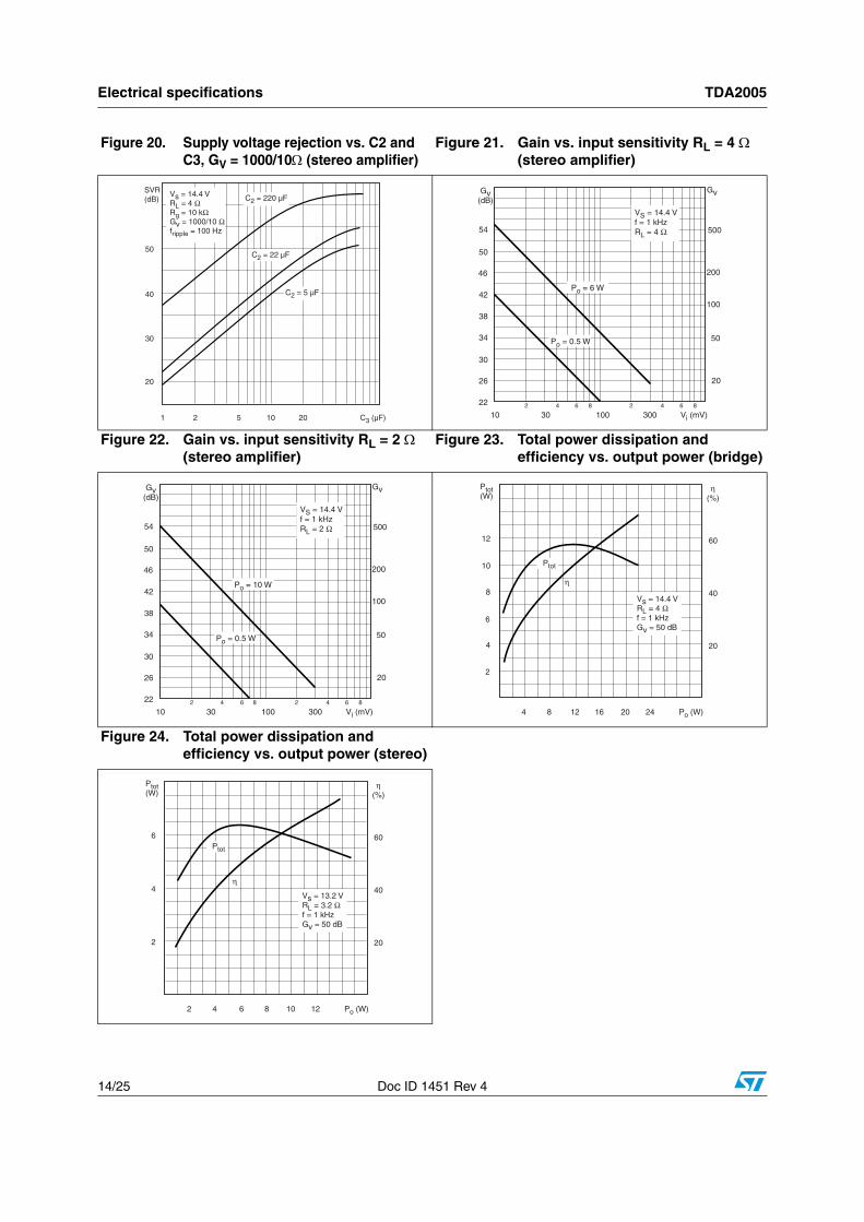
Figure 20. Supply voltage rejection vs. C2 and C3, GV = 1000/10Ω (stereo amplifier)
Figure 21. Gain vs. input sensitivity RL = 4 Ω (stereo amplifier)
Figure 22. Gain vs. input sensitivity RL = 2 Ω (stereo amplifier)
Figure 23. Total power dissipation and efficiency vs. output power (bridge)
Figure 24. Total power dissipation and efficiency vs. output power (stereo)
SVR(dB)
50
40
30
20
10 20 C3 (µF)1 2 5
Vs = 14.4 VRL = 4 ΩRg = 10 kΩGv = 1000/10 Ωfripple = 100 Hz
C2 = 220 µF
C2 = 22 µF
C2 = 5 µF
Gv(dB)
54
50
46
42
38
34
30
20
50
26
22
10 100
100
200
500
300 Vi (mV)
VS = 14.4 Vf = 1 kHzRL = 4 Ω
Po = 6 W
Po = 0.5 W
30
Gv
2 4 6 8 2 4 6 8
Gv(dB)
54
50
46
42
38
34
30
20
50
26
22
10 100
100
200
500
300 Vi (mV)
VS = 14.4 Vf = 1 kHzRL = 2 Ω
Po = 10 W
Po = 0.5 W
30
Gv
2 4 6 8 2 4 6 8
Ptot(W)
10
60
40
20
12
η(%)
η
2
4
6
8
20 24 Po (W)84 12 16
Vs = 14.4 VRL = 4 Ωf = 1 kHzGv = 50 dB
Ptot
Ptot(W)
60
40
20
6
η(%)
η
2
4
10 12 Po (W)42 6 8
Vs = 13.2 VRL = 3.2 Ωf = 1 kHzGv = 50 dB
Ptot
TDA2005 Application suggestion
Doc ID 1451 Rev 4 15/25
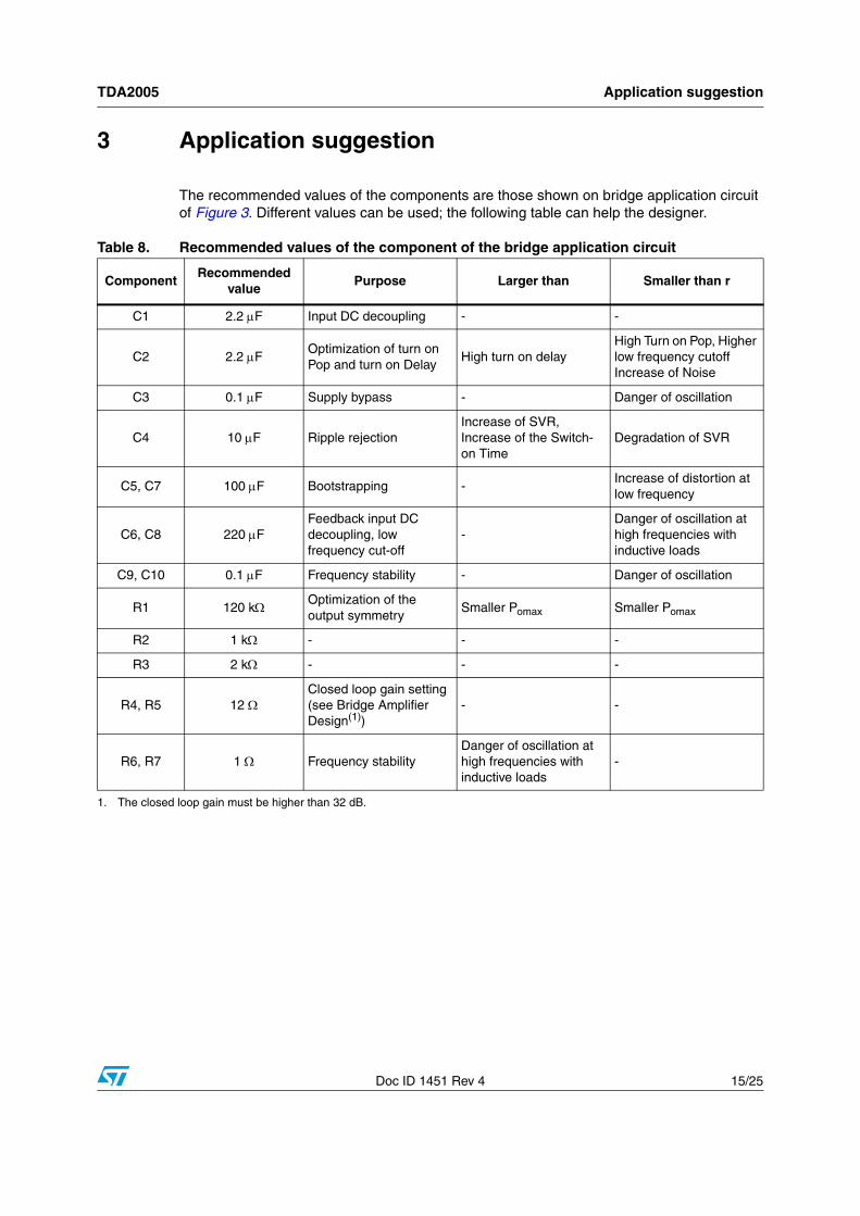
3 Application suggestion
The recommended values of the components are those shown on bridge application circuit of Figure 3. Different values can be used; the following table can help the designer.
Table 8. Recommended values of the component of the bridge application circuit
ComponentRecommended
valuePurpose Larger than Smaller than r
C1 2.2 μF Input DC decoupling - -
C2 2.2 μFOptimization of turn on Pop and turn on Delay
High turn on delayHigh Turn on Pop, Higher low frequency cutoff Increase of Noise
C3 0.1 μF Supply bypass - Danger of oscillation
C4 10 μF Ripple rejectionIncrease of SVR, Increase of the Switch-on Time
Degradation of SVR
C5, C7 100 μF Bootstrapping -Increase of distortion at low frequency
C6, C8 220 μFFeedback input DC decoupling, low frequency cut-off
-Danger of oscillation at high frequencies with inductive loads
C9, C10 0.1 μF Frequency stability - Danger of oscillation
R1 120 kΩOptimization of the output symmetry
Smaller Pomax Smaller Pomax
R2 1 kΩ - - -
R3 2 kΩ - - -
R4, R5 12 ΩClosed loop gain setting (see Bridge Amplifier Design(1))
- -
R6, R7 1 Ω Frequency stabilityDanger of oscillation at high frequencies with inductive loads
-
1. The closed loop gain must be higher than 32 dB.
Application information TDA2005
16/25 Doc ID 1451 Rev 4
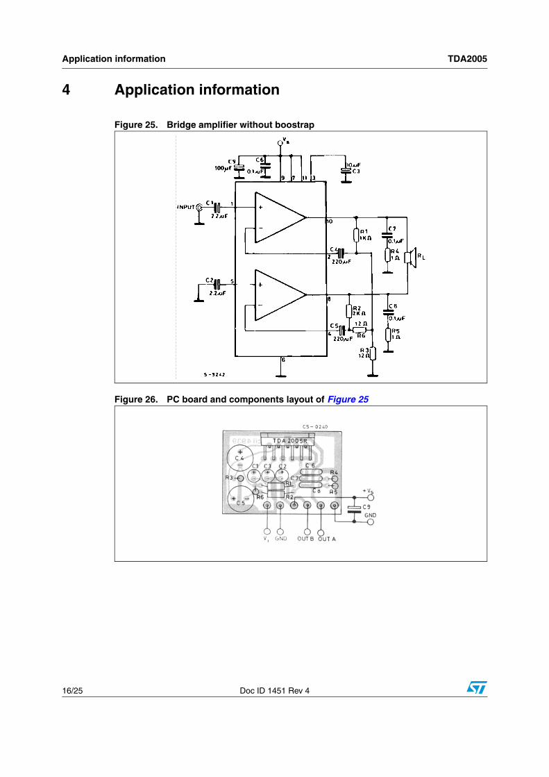
4 Application information
Figure 25. Bridge amplifier without boostrap
Figure 26. PC board and components layout of Figure 25
TDA2005 Application information
Doc ID 1451 Rev 4 17/25
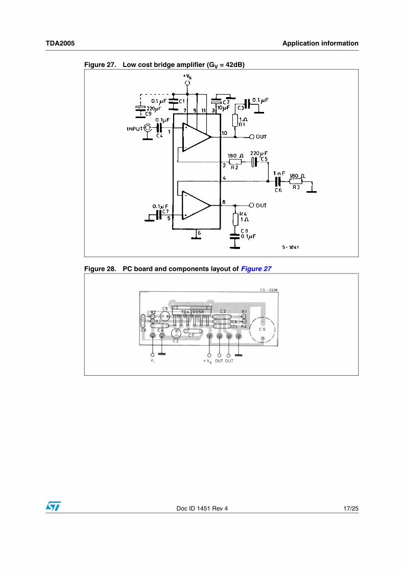
Figure 27. Low cost bridge amplifier (GV = 42dB)
Figure 28. PC board and components layout of Figure 27
Application information TDA2005
18/25 Doc ID 1451 Rev 4
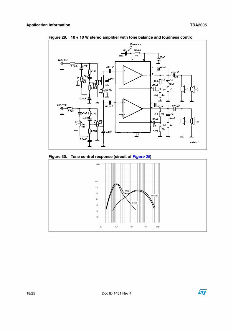
Figure 29. 10 + 10 W stereo amplifier with tone balance and loudness control
Figure 30. Tone control response (circuit of Figure 29)
(dB)
+6
+3
-3
-9
-12
10 f (Hz)102 103 104
-6
0MID
BASS
TREBLE
TDA2005 Application information
Doc ID 1451 Rev 4 19/25
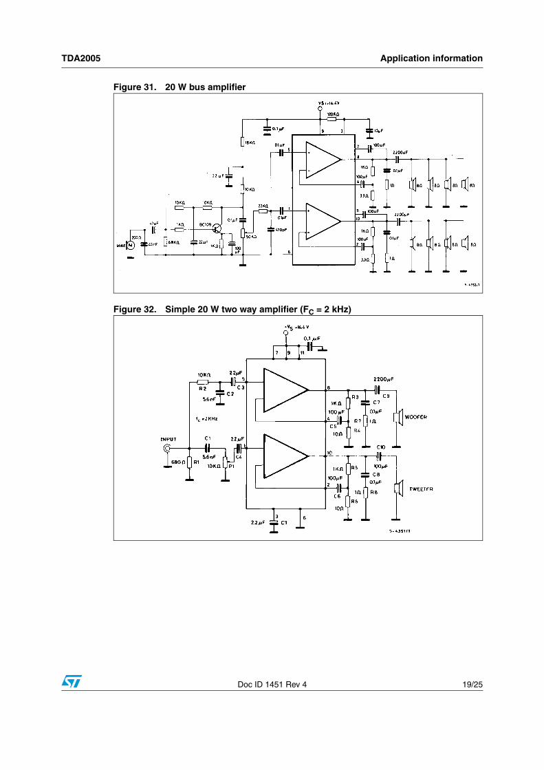
Figure 31. 20 W bus amplifier
Figure 32. Simple 20 W two way amplifier (FC = 2 kHz)
Application information TDA2005
20/25 Doc ID 1451 Rev 4
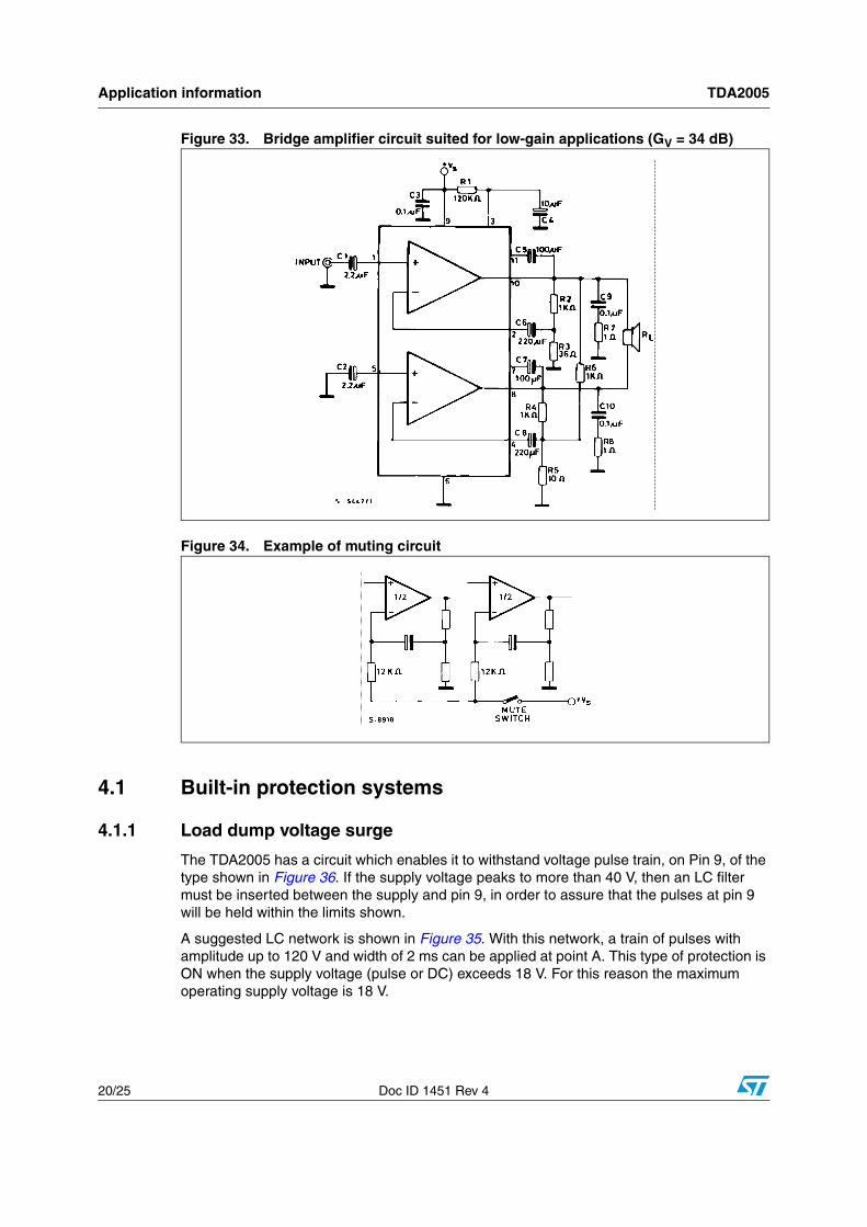
Figure 33. Bridge amplifier circuit suited for low-gain applications (GV = 34 dB)
Figure 34. Example of muting circuit
4.1 Built-in protection systems
4.1.1 Load dump voltage surge
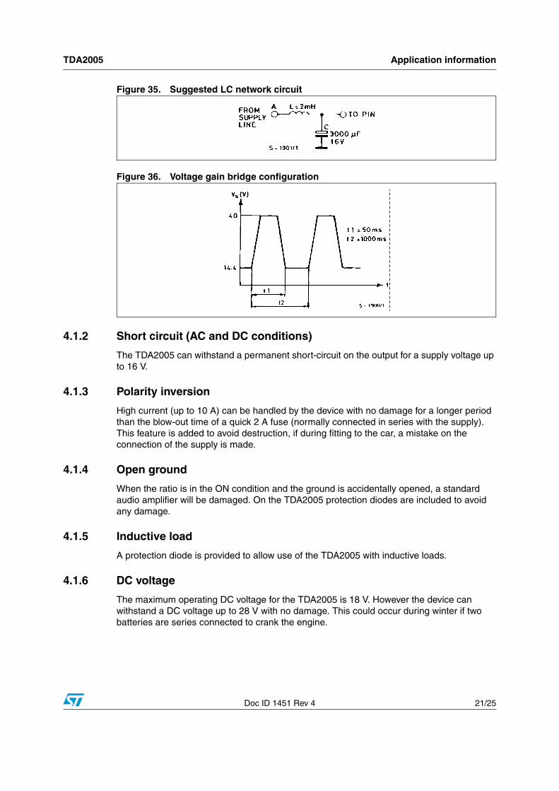
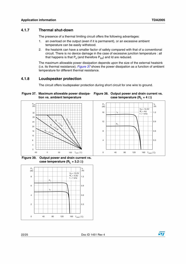
The TDA2005 has a circuit which enables it to withstand voltage pulse train, on Pin 9, of the type shown in Figure 36. If the supply voltage peaks to more than 40 V, then an LC filter must be inserted between the supply and pin 9, in order to assure that the pulses at pin 9 will be held within the limits shown.
A suggested LC network is shown in Figure 35. With this network, a train of pulses with amplitude up to 120 V and width of 2 ms can be applied at point A. This type of protection is ON when the supply voltage (pulse or DC) exceeds 18 V. For this reason the maximum operating supply voltage is 18 V.
TDA2005 Application information
Doc ID 1451 Rev 4 21/25
Figure 35. Suggested LC network circuit
Figure 36. Voltage gain bridge configuration
4.1.2 Short circuit (AC and DC conditions)
The TDA2005 can withstand a permanent short-circuit on the output for a supply voltage up to 16 V.
4.1.3 Polarity inversion
High current (up to 10 A) can be handled by the device with no damage for a longer period than the blow-out time of a quick 2 A fuse (normally connected in series with the supply). This feature is added to avoid destruction, if during fitting to the car, a mistake on the connection of the supply is made.
4.1.4 Open ground
When the ratio is in the ON condition and the ground is accidentally opened, a standard audio amplifier will be damaged. On the TDA2005 protection diodes are included to avoid any damage.
4.1.5 Inductive load
A protection diode is provided to allow use of the TDA2005 with inductive loads.
4.1.6 DC voltage
The maximum operating DC voltage for the TDA2005 is 18 V. However the device can withstand a DC voltage up to 28 V with no damage. This could occur during winter if two batteries are series connected to crank the engine.
Application information TDA2005
22/25 Doc ID 1451 Rev 4
4.1.7 Thermal shut-down
The presence of a thermal limiting circuit offers the following advantages:
1. an overload on the output (even if it is permanent), or an excessive ambient temperature can be easily withstood.
2. the heatsink can have a smaller factor of safety compared with that of a conventional circuit. There is no device damage in the case of excessive junction temperature : all that happens is that Po (and therefore Ptot) and Id are reduced.
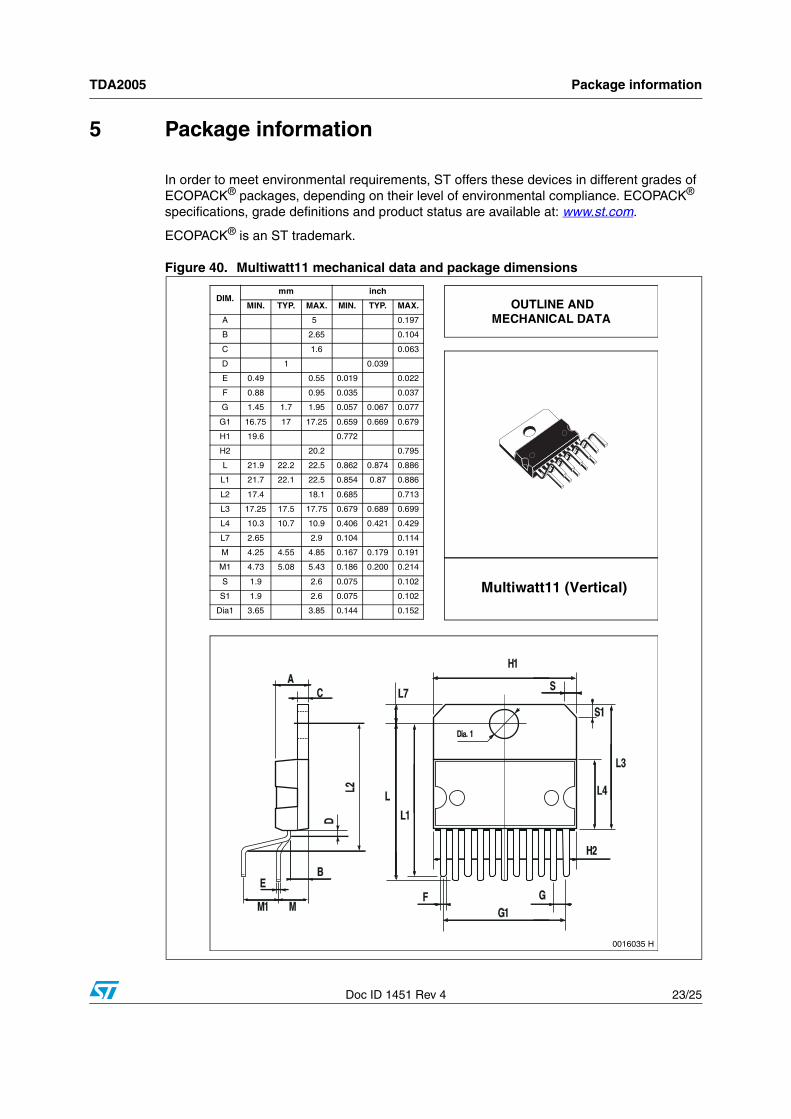
The maximum allowable power dissipation depends upon the size of the external heatsink (i.e. its thermal resistance); Figure 37 shows the power dissipation as a function of ambient temperature for different thermal resistance.
4.1.8 Loudspeaker protection
The circuit offers loudspeaker protection during short circuit for one wire to ground.
Figure 37. Maximum allowable power dissipa-tion vs. ambient temperature
Figure 38. Output power and drain current vs. case temperature (RL = 4 Ω)
Figure 39. Output power and drain current vs. case temperature (RL = 3.2 Ω)
Ptot(W)
32
28
24
20
-50 50 100 Tamb (˚C)0
16
12
8
4
0
Rth = 8˚C/W
Rth = 4˚C/W
Rth = 2˚C/W
INFIN
ITE HEATSIN
K
Po(W)
Tcase (˚C)
16
12
8
4
1.2
0.9
0.6
0.3
0 40 80 120 160
Id(A)
Id
Po
VS = 14.4VRL = 4Ωf = 1 kHz
Po(W)
Tcase (˚C)
8
6
4
2
1.2
0.9
0.6
0.3
0 40 80 120 160
Id(A)
Id
Po
VS = 13.2VRL = 3.2Ωf = 1 kHz
TDA2005 Package information
Doc ID 1451 Rev 4 23/25
5 Package information
In order to meet environmental requirements, ST offers these devices in different grades of ECOPACK® packages, depending on their level of environmental compliance. ECOPACK®
specifications, grade definitions and product status are available at: www.st.com.
ECOPACK® is an ST trademark.
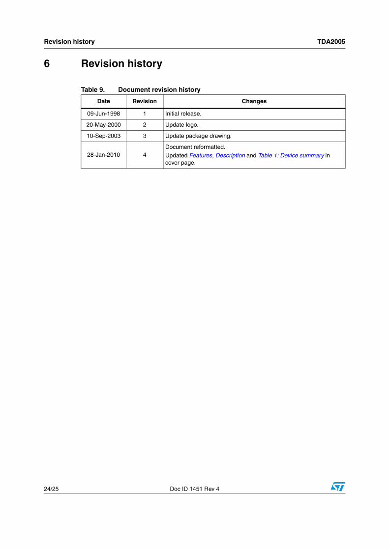
Figure 40. Multiwatt11 mechanical data and package dimensions
OUTLINE ANDMECHANICAL DATA
0016035 H
DIM.mm inch
MIN. TYP. MAX. MIN. TYP. MAX.
A 5 0.197
B 2.65 0.104
C 1.6 0.063
D 1 0.039
E 0.49 0.55 0.019 0.022
F 0.88 0.95 0.035 0.037
G 1.45 1.7 1.95 0.057 0.067 0.077
G1 16.75 17 17.25 0.659 0.669 0.679
H1 19.6 0.772
H2 20.2 0.795
L 21.9 22.2 22.5 0.862 0.874 0.886
L1 21.7 22.1 22.5 0.854 0.87 0.886
L2 17.4 18.1 0.685 0.713
L3 17.25 17.5 17.75 0.679 0.689 0.699
L4 10.3 10.7 10.9 0.406 0.421 0.429
L7 2.65 2.9 0.104 0.114
M 4.25 4.55 4.85 0.167 0.179 0.191
M1 4.73 5.08 5.43 0.186 0.200 0.214
S 1.9 2.6 0.075 0.102
S1 1.9 2.6 0.075 0.102
Dia1 3.65 3.85 0.144 0.152
Multiwatt11 (Vertical)
Revision history TDA2005
24/25 Doc ID 1451 Rev 4
6 Revision history
Table 9. Document revision history
Date Revision Changes
09-Jun-1998 1 Initial release.
20-May-2000 2 Update logo.
10-Sep-2003 3 Update package drawing.
28-Jan-2010 4Document reformatted.
Updated Features, Description and Table 1: Device summary in cover page.
TDA2005
Doc ID 1451 Rev 4 25/25
Please Read Carefully:
Information in this document is provided solely in connection with ST products. STMicroelectronics NV and its subsidiaries (“ST”) reserve theright to make changes, corrections, modifications or improvements, to this document, and the products and services described herein at anytime, without notice.
All ST products are sold pursuant to ST’s terms and conditions of sale.
Purchasers are solely responsible for the choice, selection and use of the ST products and services described herein, and ST assumes noliability whatsoever relating to the choice, selection or use of the ST products and services described herein.
No license, express or implied, by estoppel or otherwise, to any intellectual property rights is granted under this document. If any part of thisdocument refers to any third party products or services it shall not be deemed a license grant by ST for the use of such third party productsor services, or any intellectual property contained therein or considered as a warranty covering the use in any manner whatsoever of suchthird party products or services or any intellectual property contained therein.
UNLESS OTHERWISE SET FORTH IN ST’S TERMS AND CONDITIONS OF SALE ST DISCLAIMS ANY EXPRESS OR IMPLIEDWARRANTY WITH RESPECT TO THE USE AND/OR SALE OF ST PRODUCTS INCLUDING WITHOUT LIMITATION IMPLIEDWARRANTIES OF MERCHANTABILITY, FITNESS FOR A PARTICULAR PURPOSE (AND THEIR EQUIVALENTS UNDER THE LAWSOF ANY JURISDICTION), OR INFRINGEMENT OF ANY PATENT, COPYRIGHT OR OTHER INTELLECTUAL PROPERTY RIGHT.
UNLESS EXPRESSLY APPROVED IN WRITING BY AN AUTHORIZED ST REPRESENTATIVE, ST PRODUCTS ARE NOTRECOMMENDED, AUTHORIZED OR WARRANTED FOR USE IN MILITARY, AIR CRAFT, SPACE, LIFE SAVING, OR LIFE SUSTAININGAPPLICATIONS, NOR IN PRODUCTS OR SYSTEMS WHERE FAILURE OR MALFUNCTION MAY RESULT IN PERSONAL INJURY,DEATH, OR SEVERE PROPERTY OR ENVIRONMENTAL DAMAGE. ST PRODUCTS WHICH ARE NOT SPECIFIED AS "AUTOMOTIVEGRADE" MAY ONLY BE USED IN AUTOMOTIVE APPLICATIONS AT USER’S OWN RISK.
Resale of ST products with provisions different from the statements and/or technical features set forth in this document shall immediately voidany warranty granted by ST for the ST product or service described herein and shall not create or extend in any manner whatsoever, anyliability of ST.
ST and the ST logo are trademarks or registered trademarks of ST in various countries.
Information in this document supersedes and replaces all information previously supplied.
The ST logo is a registered trademark of STMicroelectronics. All other names are the property of their respective owners.
© 2010 STMicroelectronics - All rights reserved
STMicroelectronics group of companies
Australia - Belgium - Brazil - Canada - China - Czech Republic - Finland - France - Germany - Hong Kong - India - Israel - Italy - Japan - Malaysia - Malta - Morocco - Philippines - Singapore - Spain - Sweden - Switzerland - United Kingdom - United States of America
www.st.com