TDA8944J 2 x 7 W stereo Bridge Tied Load (BTL) …TDA8944J 2 x 7 W stereo Bridge Tied Load (BTL)...
22
TDA8944J 2 x 7 W stereo Bridge Tied Load (BTL) audio amplifier Rev. 02 — 14 February 2000 Product specification c c 1. General description The TDA8944J is a dual-channel audio power amplifier with an output power of 2 × 7 W at an 8 Ω load and a 12 V supply. The circuit contains two Bridge Tied Load (BTL) amplifiers with an all-NPN output stage and standby/mute logic. The TDA8944J comes in a 17-pin DIL-bent-SIL (DBS) power package. The TDA8944J is printed-circuit board (PCB) compatible with all other types in the TDA894x family. One PCB footprint accommodates both the mono and the stereo products. 2. Features Few external components Fixed gain Standby and mute mode No on/off switching plops Low standby current High supply voltage ripple rejection Outputs short-circuit protected to ground, supply and across the load Thermally protected Printed-circuit board compatible. 3. Applications Mains fed applications (e.g. TV sound) PC audio Portable audio. 4. Quick reference data Table 1: Quick reference data Symbol Parameter Conditions Min Typ Max Unit V CC supply voltage 6 12 18 V I q quiescent supply current V CC = 12 V; R L = ∞ - 24 36 mA I stb standby supply current - - 10 μA
Transcript of TDA8944J 2 x 7 W stereo Bridge Tied Load (BTL) …TDA8944J 2 x 7 W stereo Bridge Tied Load (BTL)...
TDA8944J2 x 7 W stereo Bridge Tied Load (BTL) audio amplifierRev. 02 — 14 February 2000 Product specification
c
c
1. General description
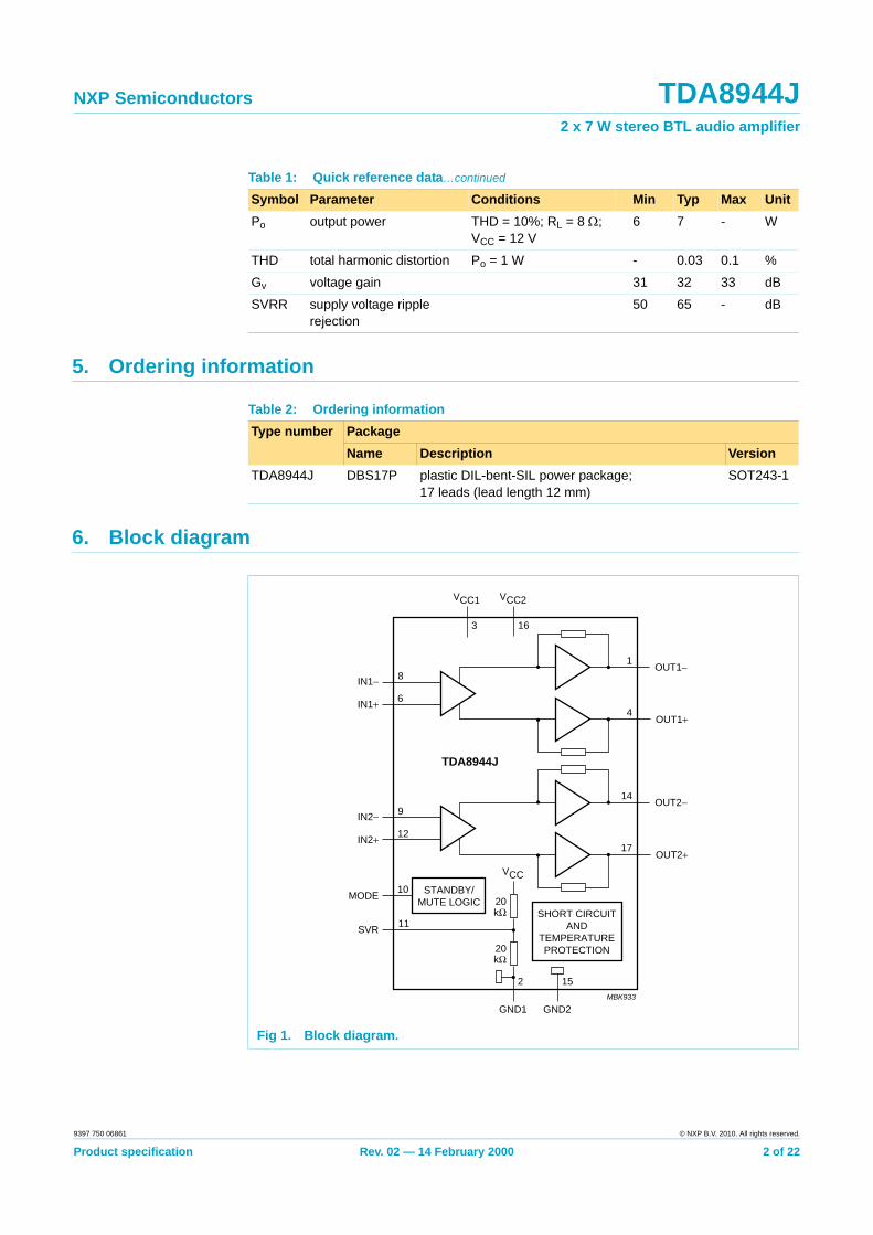
The TDA8944J is a dual-channel audio power amplifier with an output power of 2 × 7 W at an 8 Ω load and a 12 V supply. The circuit contains two Bridge Tied Load (BTL) amplifiers with an all-NPN output stage and standby/mute logic. The TDA8944J comes in a 17-pin DIL-bent-SIL (DBS) power package. The TDA8944J is printed-circuit board (PCB) compatible with all other types in the TDA894x family. One PCB footprint accommodates both the mono and the stereo products.
2. Features
Few external componentsFixed gainStandby and mute modeNo on/off switching plopsLow standby currentHigh supply voltage ripple rejectionOutputs short-circuit protected to ground, supply and across the loadThermally protectedPrinted-circuit board compatible.
3. Applications
Mains fed applications (e.g. TV sound)PC audio Portable audio.
4. Quick reference data
Table 1: Quick reference dataSymbol Parameter Conditions Min Typ Max UnitVCC supply voltage 6 12 18 V
Iq quiescent supply current VCC = 12 V; RL = ∞ - 24 36 mA
Istb standby supply current - - 10 μA
NXP Semiconductors TDA8944J2 x 7 W stereo BTL audio amplifier
5. Ordering information
6. Block diagram
Po output power THD = 10%; RL = 8 Ω; VCC = 12 V
6 7 - W
THD total harmonic distortion Po = 1 W - 0.03 0.1 %
Gv voltage gain 31 32 33 dB
SVRR supply voltage ripple rejection
50 65 - dB
Table 1: Quick reference data…continued
Symbol Parameter Conditions Min Typ Max Unit
Table 2: Ordering informationType number Package
Name Description VersionTDA8944J DBS17P plastic DIL-bent-SIL power package;
17 leads (lead length 12 mm)SOT243-1
Fig 1. Block diagram.
width
MBK933
STANDBY/MUTE LOGIC
SHORT CIRCUITAND
TEMPERATUREPROTECTION
20kΩ
20kΩ
9
1217
14
10
11
VCC1
VCC
2
3
OUT2+
GND1
15
GND2
SVR
OUT2−IN2−
IN2+
8
TDA8944J
64
1
VCC2
16
OUT1+
OUT1−IN1−
IN1+
MODE
Product specification Rev. 02 — 14 February 2000 2 of 229397 750 06861 © NXP B.V. 2010. All rights reserved.
NXP Semiconductors TDA8944J2 x 7 W stereo BTL audio amplifier
7. Pinning information
7.1 Pinning
7.2 Pin description
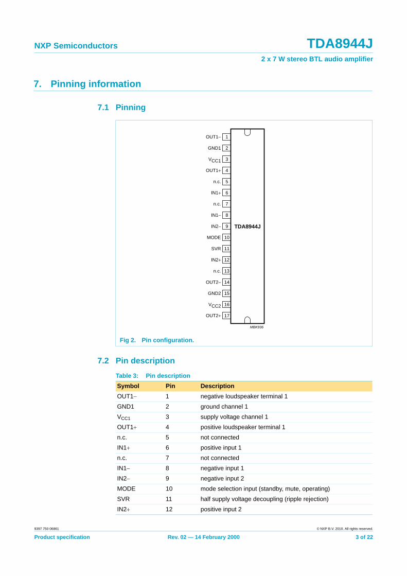
Fig 2. Pin configuration.
handbook, halfpage
TDA8944J
MBK936
1
2
3
4
5
6
7
8
9
10
11
12
13
14
15
16
17
OUT1−
GND1
VCC1
OUT1+
n.c.
IN1+
n.c.
IN1−
IN2−
MODE
SVR
IN2+
n.c.
OUT2+
GND2
VCC2
OUT2−
Table 3: Pin descriptionSymbol Pin DescriptionOUT1− 1 negative loudspeaker terminal 1
GND1 2 ground channel 1
VCC1 3 supply voltage channel 1
OUT1+ 4 positive loudspeaker terminal 1
n.c. 5 not connected
IN1+ 6 positive input 1
n.c. 7 not connected
IN1− 8 negative input 1
IN2− 9 negative input 2
MODE 10 mode selection input (standby, mute, operating)
SVR 11 half supply voltage decoupling (ripple rejection)
IN2+ 12 positive input 2
Product specification Rev. 02 — 14 February 2000 3 of 229397 750 06861 © NXP B.V. 2010. All rights reserved.
NXP Semiconductors TDA8944J2 x 7 W stereo BTL audio amplifier
8. Functional description
The TDA8944J is a stereo BTL audio power amplifier capable of delivering 2 × 7 W output power to an 8 Ω load at THD = 10%, using a 12 V power supply and an external heatsink. The voltage gain is fixed at 32 dB.
With the three-level MODE input the device can be switched from ‘standby’ to ‘mute’ and to ‘operating’ mode.
The TDA8944J outputs are protected by an internal thermal shutdown protection mechanism and a short-circuit protection.
8.1 Input configurationThe TDA8944J inputs can be driven symmetrical (floating) as well as asymmetrical. In the asymmetrical mode one input pin is connected via a capacitor to the signal ground which should be as close as possible to the SVR (electrolytic) capacitor ground. Note that the DC level of the input pins is half of the supply voltage VCC, so coupling capacitors for both pins are necessary.
The input cut-off frequency is:
(1)
For Ri = 45 kΩ and Ci = 220 nF:
(2)
As shown in Equation 1 and 2, large capacitor values for the inputs are not necessary; so the switch-on delay during charging of the input capacitors, can be minimized. This results in a good low frequency response and good switch-on behaviour.
Remark: To prevent HF oscillations do not leave the inputs open, connect a capacitor of at least 1.5 nF across the input pins close to the device.
n.c. 13 not connected
OUT2− 14 negative loudspeaker terminal 2
GND2 15 ground channel 2
VCC2 16 supply voltage channel 2
OUT2+ 17 positive loudspeaker terminal 2
Table 3: Pin description…continued
Symbol Pin Description
fi cut off–( )1
2 Ri Ci×( )–------------------------------=
fi cut off–( )1
2 45 103× 220× 10 9–×( )–------------------------------------------------------------------- 16 Hz= =
Product specification Rev. 02 — 14 February 2000 4 of 229397 750 06861 © NXP B.V. 2010. All rights reserved.
NXP Semiconductors TDA8944J2 x 7 W stereo BTL audio amplifier
8.2 Power amplifierThe power amplifier is a Bridge Tied Load (BTL) amplifier with an all-NPN output stage, capable of delivering a peak output current of 2 A.
The BTL principle offers the following advantages:
• Lower peak value of the supply current
• The ripple frequency on the supply voltage is twice the signal frequency
• No expensive DC-blocking capacitor
• Good low frequency performance.
8.2.1 Output power measurementThe output power as a function of the supply voltage is measured on the output pins at THD = 10%; see Figure 8. The maximum output power is limited by the maximum supply voltage of 12 V and the maximum available output current: 2 A repetitive peak current.
8.2.2 HeadroomTypical CD music requires at least 12 dB (factor 15.85) dynamic headroom – compared to the average power output – for transferring the loudest parts without distortion. At VCC = 12 V, RL = 8 Ω and Po = 4 W at THD = 0.1% (see Figure 6), the Average Listening Level (ALL) – music power – without any distortion yields:
Po(ALL) = 4 W/15.85 = 252 mW.
The power dissipation can be derived from Figure 11 on page 10 for 0 dB respectively 12 dB headroom.
For the average listening level a power dissipation of 4 W can be used for a heatsink calculation.
8.3 Mode selectionThe TDA8944J has three functional modes, which can be selected by applying the proper DC voltage to pin MODE. See Figure 4 and 5 for the respective DC levels, which depend on the supply voltage level. The MODE pin can be driven by a 3-state logic output stage: e.g. a microcontroller with additional components for DC-level shifting.
Standby — In this mode the current consumption is very low and the outputs are floating. The device is in standby mode when (VCC − 0.5 V) < VMODE < VCC, or when the MODE pin is left floating (high impedance). The power consumption of the TDA8944J will be reduced to <0.18 mW.
Table 4: Power rating as function of headroomHeadroom Power output (THD = 0.1%) Power dissipation (P)0 dB Po = 4 W 8 W
12 dB Po(ALL) = 252 mW 4 W
Product specification Rev. 02 — 14 February 2000 5 of 229397 750 06861 © NXP B.V. 2010. All rights reserved.
NXP Semiconductors TDA8944J2 x 7 W stereo BTL audio amplifier
Mute — In this mode the amplifier is DC-biased but not operational (no audio output); the DC level of the input and output pins remain on half the supply voltage. This allows the input coupling and Supply Voltage Ripple Rejection (SVRR) capacitors to be charged to avoid pop-noise. The device is in mute mode when 3 V < VMODE < (VCC − 1.5 V).
Operating — In this mode the amplifier is operating normally. The operating mode is activated at VMODE < 0.5 V.
8.3.1 Switch-on and switch-offTo avoid audible plops during supply voltage switch-on or switch-off, the device is set to standby mode before the supply voltage is applied (switch-on) or removed (switch-off).
The switch-on and switch-off time can be influenced by an RC-circuit on the MODE pin. Rapid on/off switching of the device or the MODE pin may cause ‘click- and pop-noise’. This can be prevented by proper timing of the RC-circuit on the MODE pin.
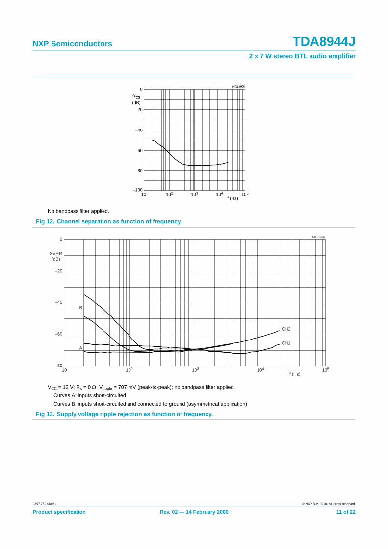
8.4 Supply Voltage Ripple Rejection (SVRR)The SVRR is measured with an electrolytic capacitor of 10 μF on pin SVR at a bandwidth of 10 Hz to 80 kHz. Figure 13 on page 11 illustrates the SVRR as function of the frequency. A larger capacitor value on the SVR pin improves the ripple rejection behaviour at the lower frequencies.
8.5 Built-in protection circuitsThe TDA8944J contains two types of protection circuits, i.e. short-circuit and thermal shutdown.
8.5.1 Short-circuit protection
Short-circuit to ground or supply line — This is detected by a so-called ‘missing current’ detection circuit which measures the current in the positive supply line and the current in the ground line. A difference between both currents larger than 0.4 A, switches the power stage to standby mode (high impedance).
Short-circuit across the load — This is detected by an absolute-current measurement. An absolute-current larger than 2 A, switches the power stage to standby mode (high impedance).
8.5.2 Thermal shutdown protectionThe junction temperature is measured by a temperature sensor; at a junction temperature of approximately 150 °C this detection circuit switches the power stage to standby mode (high impedance).
Product specification Rev. 02 — 14 February 2000 6 of 229397 750 06861 © NXP B.V. 2010. All rights reserved.
NXP Semiconductors TDA8944J2 x 7 W stereo BTL audio amplifier
9. Limiting values
10. Thermal characteristics
11. Static characteristics
[1] With a load connected at the outputs the quiescent current will increase, the maximum of this increase being equal to the differential output voltage offset (ΔVOUT) divided by the load resistance (RL).
[2] The DC output voltage with respect to ground is approximately 0.5VCC.[3] ΔVOUT = ⎪VOUT+ − VOUT− ⎪
Table 5: Limiting valuesIn accordance with the Absolute Maximum Rating System (IEC 60134).
Symbol Parameter Conditions Min Max UnitVCC supply voltage no signal −0.3 +25 V
operating −0.3 +18 V
VI input voltage −0.3 VCC + 0.3 V
IORM repetitive peak output current - 2 A
Tstg storage temperature non-operating −55 +150 °C
Tamb operating ambient temperature −40 +85 °C
Ptot total power dissipation - 18 W
VCC(sc) supply voltage to guarantee short-circuit protection
- 15 V
Table 6: Thermal characteristicsSymbol Parameter Conditions Value UnitRth(j-a) thermal resistance from junction to ambient in free air 40 K/W
Rth(j-mb) thermal resistance from junction to mounting base both channels driven 6.9 K/W
Table 7: Static characteristicsVCC = 12 V; Tamb = 25 °C; RL = 8 Ω; VMODE = 0 V; Vi = 0 V; measured in test circuit Figure 14; unless otherwise specified.
Symbol Parameter Conditions Min Typ Max UnitVCC supply voltage operating 6 12 18 V
Iq quiescent supply current RL = ∞ [1] - 24 36 mA
Istb standby supply current VMODE = VCC - - 10 μA
VO DC output voltage [2] - 6 - V
ΔVOUT [3] differential output voltage offset - - 200 mV
VMODE mode selection input voltage operating mode 0 - 0.5 V
mute mode 3 - VCC − 1.5 V
standby mode VCC − 0.5 - VCC V
IMODE mode selection input current 0 < VMODE < VCC - - 20 μA
Product specification Rev. 02 — 14 February 2000 7 of 229397 750 06861 © NXP B.V. 2010. All rights reserved.
NXP Semiconductors TDA8944J2 x 7 W stereo BTL audio amplifier
12. Dynamic characteristics
[1] The noise output voltage is measured at the output in a frequency range from 20 Hz to 20 kHz (unweighted), with a source impedance Rs = 0 Ω at the input.
[2] Supply voltage ripple rejection is measured at the output, with a source impedance Rs = 0 Ω at the input. The ripple voltage is a sine wave with a frequency fripple and an amplitude of 707 mV (RMS), which is applied to the positive supply rail.
[3] Output voltage in mute mode is measured with an input voltage of 1 V (RMS) in a bandwidth of 20 kHz, so including noise.
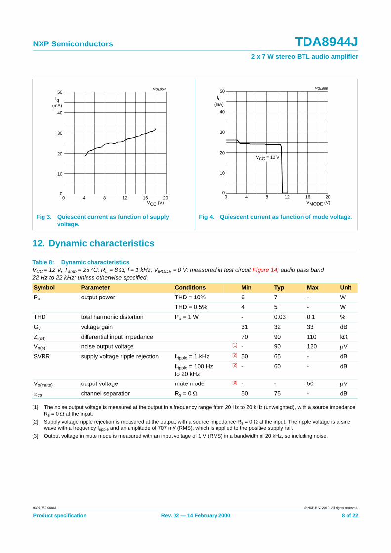
Fig 3. Quiescent current as function of supply voltage.
Fig 4. Quiescent current as function of mode voltage.
handbook, halfpage50
40
30
20
10
00 4 8 12 16
VCC (V)
Iq(mA)
20
MGL954
handbook, halfpage50
40
30
20
10
00 4 8 12 16
VMODE (V)
Iq(mA)
20
MGL955
VCC = 12 V
Table 8: Dynamic characteristicsVCC = 12 V; Tamb = 25 °C; RL = 8 Ω; f = 1 kHz; VMODE = 0 V; measured in test circuit Figure 14; audio pass band 22 Hz to 22 kHz; unless otherwise specified.
Symbol Parameter Conditions Min Typ Max UnitPo output power THD = 10% 6 7 - W
THD = 0.5% 4 5 - W
THD total harmonic distortion Po = 1 W - 0.03 0.1 %
Gv voltage gain 31 32 33 dB
Zi(dif) differential input impedance 70 90 110 kΩ
Vn(o) noise output voltage [1] - 90 120 μV
SVRR supply voltage ripple rejection fripple = 1 kHz [2] 50 65 - dB
fripple = 100 Hz to 20 kHz
[2] - 60 - dB
Vo(mute) output voltage mute mode [3] - - 50 μV
αcs channel separation Rs = 0 Ω 50 75 - dB
Product specification Rev. 02 — 14 February 2000 8 of 229397 750 06861 © NXP B.V. 2010. All rights reserved.
NXP Semiconductors TDA8944J2 x 7 W stereo BTL audio amplifier
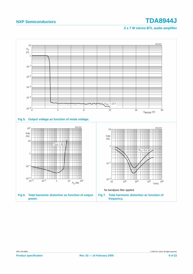
Fig 5. Output voltage as function of mode voltage.
No bandpass filter applied.
Fig 6. Total harmonic distortion as function of output power.
Fig 7. Total harmonic distortion as function of frequency.
handbook, full pagewidth
2016VMODE (V)
12
MGL957
840
Vo(V)
10
1
10−3
10−2
10−1
10−4
10−5
VCC = 12 V
handbook, halfpage
THD(%)
10−2 10210110−1
Po (W)
102
10
1
10−1
10−2
MGL952
VCC = 12 V
handbook, halfpage
THD(%)
10 105102 103 104
f (Hz)
1
10
10−1
10−2
MGL953
Po = 0.1 W
1 W
Product specification Rev. 02 — 14 February 2000 9 of 229397 750 06861 © NXP B.V. 2010. All rights reserved.
NXP Semiconductors TDA8944J2 x 7 W stereo BTL audio amplifier
THD = 10%.
Fig 8. Output power as function of supply voltage. Fig 9. Total power dissipation as function of supply voltage.
VCC = 12 V.
Fig 10. Efficiency as function of output power. Fig 11. Power dissipation as function of output power.
handbook, halfpage20
16
12
8
4
00 4 8 12 16
VCC (V)
Po(W)
20
MGL959
RL = 8 Ω
16 Ω
handbook, halfpage20
16
12
8
4
00 4 8 12 16
VCC (V)
Ptot(W)
20
MGL960
RL = 8 Ω
16 Ω
handbook, halfpage100
80
60
40
20
00 2 4 6 8
Po (W)
η(%)
10
MGL962
RL = 16 Ω
8 Ω
handbook, halfpage10
8
6
4
2
00 2 4 6 8
Po (W)
P
(W)
10
MGL961
RL = 8 Ω
16 Ω
Product specification Rev. 02 — 14 February 2000 10 of 229397 750 06861 © NXP B.V. 2010. All rights reserved.
NXP Semiconductors TDA8944J2 x 7 W stereo BTL audio amplifier
No bandpass filter applied.
Fig 12. Channel separation as function of frequency.
VCC = 12 V; Rs = 0 Ω; Vripple = 707 mV (peak-to-peak); no bandpass filter applied.Curves A: inputs short-circuitedCurves B: inputs short-circuited and connected to ground (asymmetrical application)
Fig 13. Supply voltage ripple rejection as function of frequency.
handbook, halfpage0
−20
−40
−60
−80
−10010 102 103 104 105
f (Hz)
αcs(dB)
MGL958
handbook, full pagewidth
SVRR(dB)
102 103 104 10510f (Hz)
−20
0
−40
−60
−80
MGL956
CH2
B
ACH1
Product specification Rev. 02 — 14 February 2000 11 of 229397 750 06861 © NXP B.V. 2010. All rights reserved.
NXP Semiconductors TDA8944J2 x 7 W stereo BTL audio amplifier
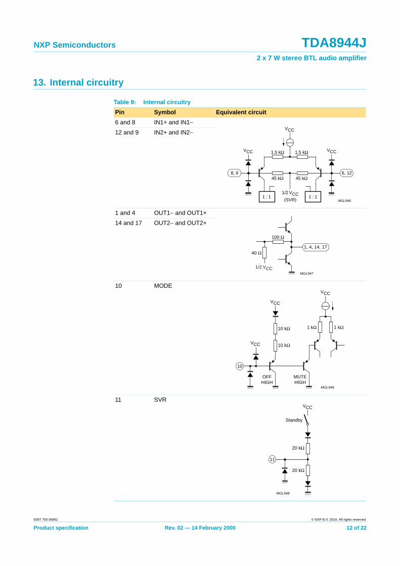
13. Internal circuitry
Table 9: Internal circuitryPin Symbol Equivalent circuit6 and 8 IN1+ and IN1−
12 and 9 IN2+ and IN2−
1 and 4 OUT1− and OUT1+
14 and 17 OUT2− and OUT2+
10 MODE
11 SVR
1.5 kΩ 1.5 kΩ
45 kΩ 45 kΩ
VCC
VCCVCC
MGL9461 : 1 1 : 1
1/2 VCC(SVR)
8, 9 6, 12
40 Ω
100 Ω
MGL947
1, 4, 14, 17
1/2 VCC
1 kΩ10 kΩ
10 kΩ
OFFHIGH
MUTEHIGH
1 kΩ
VCC
VCC
VCC
MGL949
10
Standby
20 kΩ
20 kΩ
VCC
MGL948
11
Product specification Rev. 02 — 14 February 2000 12 of 229397 750 06861 © NXP B.V. 2010. All rights reserved.
NXP Semiconductors TDA8944J2 x 7 W stereo BTL audio amplifier
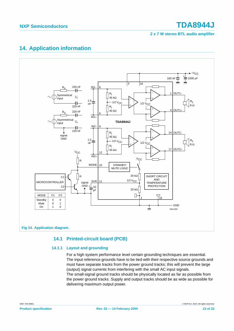
14. Application information
14.1 Printed-circuit board (PCB)
14.1.1 Layout and groundingFor a high system performance level certain grounding techniques are essential. The input reference grounds have to be tied with their respective source grounds and must have separate tracks from the power ground tracks; this will prevent the large (output) signal currents from interfering with the small AC input signals. The small-signal ground tracks should be physically located as far as possible from the power ground tracks. Supply and output tracks should be as wide as possible for delivering maximum output power.
Fig 14. Application diagram.
, ful
l pag
ewid
th
3 16
OUT1−−
−−
+
++
+
−
RL8 Ω
Ri45 kΩ
Rs
Symmetricalinput
Ri45 kΩ
RL8 Ω
OUT1+
IN1−
IN1+
OUT2−
OUT2+
GNDMGL950
IN2−
IN2+
MODE
SVR
1
8220 nF
6
9
12
10
11
4
14
17
152
+VCC
1000 μF100 nF
20 kΩ
20 kΩ
10μF
−
−−
+
++
+
−
Ri45 kΩ
Ri45 kΩ
R
C1
C2
R
VCC
VCC
signalGND
TDA8944J
signalGND
SHORT CIRCUITAND
TEMPERATUREPROTECTION
STANDBY/MUTE LOGIC
MICROCONTROLLER
Standby
MODE
MuteOn
001
0
C1 C2
10
1/2 VCC
220 nF
1.5nF
1.5nF
Ci
Rs
Asymmetricalinput
220 nF
220 nF
Ci
1/2 VCC 1/2 VCC
1/2 VCC
1/2 VCC
Product specification Rev. 02 — 14 February 2000 13 of 229397 750 06861 © NXP B.V. 2010. All rights reserved.
NXP Semiconductors TDA8944J2 x 7 W stereo BTL audio amplifier
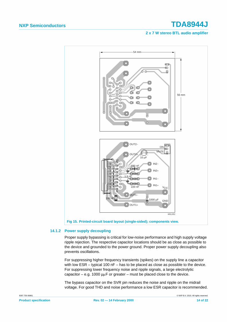
14.1.2 Power supply decouplingProper supply bypassing is critical for low-noise performance and high supply voltage ripple rejection. The respective capacitor locations should be as close as possible to the device and grounded to the power ground. Proper power supply decoupling also prevents oscillations.
For suppressing higher frequency transients (spikes) on the supply line a capacitor with low ESR – typical 100 nF – has to be placed as close as possible to the device. For suppressing lower frequency noise and ripple signals, a large electrolytic capacitor – e.g. 1000 µμF or greater – must be placed close to the device.
The bypass capacitor on the SVR pin reduces the noise and ripple on the midrail voltage. For good THD and noise performance a low ESR capacitor is recommended.
Fig 15. Printed-circuit board layout (single-sided); components view.
width
MGL951
ON
MUTE
220 nF
100 nF
1.5 nF
1000 μF
10 μF
220 nF
1
17
+ −
IN2−
IN2+
IN1−
IN1+
OUT1−
OUT1+
OUT2−
OUT2+
VCC
GND
54 mm
56 mm
Product specification Rev. 02 — 14 February 2000 14 of 229397 750 06861 © NXP B.V. 2010. All rights reserved.
NXP Semiconductors TDA8944J2 x 7 W stereo BTL audio amplifier
14.2 Thermal behaviour and heatsink calculationThe measured maximum thermal resistance of the IC package, Rth(j-mb) is 6.9 K/W. A calculation for the heatsink can be made, with the following parameters:
Tamb(max) = 50 °CVCC = 12 V and RL = 8 Ω
Tj(max) = 150 °C.Rth(tot) is the total thermal resistance between the junction and the ambient including the heatsink. In the heatsink calculations the value of Rth(mb-h) is ignored.
At VCC = 12 V and RL = 8 Ω the measured worstcase sine-wave dissipation is 8 W; see Figure 11. For Tj(max) = 150 °C the temperature raise - caused by the power dissipation - is: 150 – 50 = 100 °C.
P × Rth(tot) = 100 °CRth(tot) = 100/8 = 12.5 K/WRth(h-a) = Rth(tot) – Rth(j-mb) = 12.5 – 6.9 = 5.6 K/W.
The calculation above is for an application at worstcase (stereo) sine-wave output signals. In practice music signals will be applied, which decreases the maximum power dissipation to approximately half of the sine-wave power dissipation (see Section 8.2.2). This allows for the use of a smaller heatsink:
P × Rth(tot) = 100 °CRth(tot) = 100/4 = 25 K/WRth(h-a) = Rth(tot) – Rth(j-mb) = 25 – 6.9 = 18.1 K/W.
To increase the lifetime of the IC, Tj(max) should be reduced to 125 °C. This requires a heatsink of approximately 12 K/W for music signals.
15. Test information
15.1 Quality informationThe General Quality Specification for Integrated Circuits, SNW-FQ-611 is applicable.
15.2 Test conditionsTamb = 25 °C; VCC = 12 V; f = 1 kHz; RL = 8 Ω; audio pass band 22 Hz to 22 kHz; unless otherwise specified.
Remark: In the graphs as function of frequency no bandpass filter was applied; see Figure 7, 12 and 13.
Product specification Rev. 02 — 14 February 2000 15 of 229397 750 06861 © NXP B.V. 2010. All rights reserved.
NXP Semiconductors TDA8944J2 x 7 W stereo BTL audio amplifier
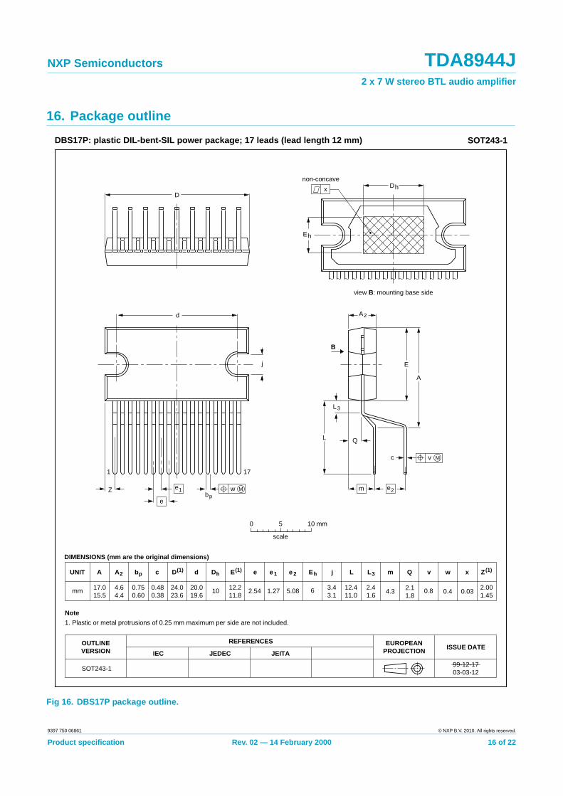
16. Package outline
Fig 16. DBS17P package outline.
REFERENCESOUTLINEVERSION
EUROPEANPROJECTION ISSUE DATE
IEC JEDEC JEITA
DIMENSIONS (mm are the original dimensions)
Note
1. Plastic or metal protrusions of 0.25 mm maximum per side are not included.
SOT243-1
0 5 10 mm
scale
D
L
E
A
c
A2
L3
Q
w Mbp
1
d
D
Z e
e
x h
1 17
j
Eh
non-concave
99-12-1703-03-12
DBS17P: plastic DIL-bent-SIL power package; 17 leads (lead length 12 mm) SOT243-1
view B: mounting base side
m 2e
v M
B
UNIT A e 1A2 bp c D(1) E(1) Z(1)d eDh L L3 m
mm 17.015.5
4.64.4
0.750.60
0.480.38
24.023.6
20.019.6
10 2.54
v
0.812.211.8
1.27
e 2
5.08 2.41.6
Eh
6 2.001.45
2.11.8
3.43.1
4.312.411.0
Qj
0.4
w
0.03
x
Product specification Rev. 02 — 14 February 2000 16 of 229397 750 06861 © NXP B.V. 2010. All rights reserved.
NXP Semiconductors TDA8944J2 x 7 W stereo BTL audio amplifier
17. Soldering
17.1 Introduction to soldering through-hole mount packagesThis text gives a brief insight to wave, dip and manual soldering. A more in-depth account of soldering ICs can be found in our Data Handbook IC26; Integrated Circuit Packages (document order number 9398 652 90011).
Wave soldering is the preferred method for mounting of through-hole mount IC packages on a printed-circuit board.
17.2 Soldering by dipping or by solder waveDriven by legislation and environmental forces the worldwide use of lead-free solder pastes is increasing. Typical dwell time of the leads in the wave ranges from 3 to 4 seconds at 250 °C or 265 °C, depending on solder material applied, SnPb or Pb-free respectively.
The total contact time of successive solder waves must not exceed 5 seconds.
The device may be mounted up to the seating plane, but the temperature of the plastic body must not exceed the specified maximum storage temperature (Tstg(max)). If the printed-circuit board has been pre-heated, forced cooling may be necessary immediately after soldering to keep the temperature within the permissible limit.
17.3 Manual solderingApply the soldering iron (24 V or less) to the lead(s) of the package, either below the seating plane or not more than 2 mm above it. If the temperature of the soldering iron bit is less than 300 °C it may remain in contact for up to 10 seconds. If the bit temperature is between 300 and 400 °C, contact may be up to 5 seconds.
17.4 Package related soldering information
[1] For SDIP packages, the longitudinal axis must be parallel to the transport direction of the printed-circuit board.
[2] For PMFP packages hot bar soldering or manual soldering is suitable.
Table 10: Suitability of through-hole mount IC packages for dipping and wave soldering methods
Package Soldering methodDipping Wave
DBS, DIP, HDIP, RDBS, SDIP, SIL suitable suitable [1]
PMFP [2] − not suitable
Product specification Rev. 02 — 14 February 2000 17 of 229397 750 06861 © NXP B.V. 2010. All rights reserved.
NXP Semiconductors TDA8944J2 x 7 W stereo BTL audio amplifier
18. Revision historyTable 11: Revision historyRev Date CPCN Description02 000214 - Product specification; second version; supersedes initial version TDA8944J-01 of
14 April 1999 (9397 750 04881). Modifications:• Table 1 on page 1: SVRR; Typ value 65 dB → added
• Figure 1 on page 2: Block diagram; pin numbers changed OUT2− → 14 and OUT2+ → 17
• Figure 2 on page 3: Pin configuration; pin numbers changed OUT2− → 14 and OUT2+ → 17
• Section 8 “Functional description”: – Section 8.1 “Input configuration” on page 4 → added.– Section 8.2 “Power amplifier” on page 5: ........, capable of delivering a peak output
current of 1.5 A → changed to 2 A.– Section 8.2.1 “Output power measurement” on page 5 → added– Section 8.2.2 “Headroom” on page 5 → added
• Section 8.3 “Mode selection”:– Standby mode: VMODE > (VCC − 0.5 V) → changed to (VCC − 0.5 V) < VMODE < VCC; The
power consumption of the TDA8944J will be reduced to <0.18 mW → added.– Mute mode: the DC level of the input and output pins remain on half the supply
voltage → added; – 2.5 V < VMODE < (VCC − 1.5 V) → changed to 3 V < VMODE < (VCC − 1.5 V)– Section 8.3.1 “Switch-on and switch-off” on page 6
• Section 8.4 “Supply Voltage Ripple Rejection (SVRR)” on page 6 → added
• Section 8.5 “Built-in protection circuits” on page 6 → added
• Table 5 on page 7: – Ptot value added 18 V– VCC(sc) value added 15 V
• Table 6 on page 7:– Rth(j-a) value added 40 K/W– Rth(j-c) value 10 → changed to 6.9 K/W; condition ‘in free air’ → changed to ‘both channels
driven’
• Table 7 on page 7: VMODE - mute mode - value Min 2.5 → changed to 3 V
• Table 8 on page 8: – SVRR; Typ values 65 and 60 dB → added– αcs; Typ value 75 dB → added
• Figure 3 to 13: figures added
• Section 13 “Internal circuitry” on page 12: → added
• Figure 14: figure adjusted
• Section 14.1 “Printed-circuit board (PCB)” on page 13: → added
• Figure 15: figure added
• Section 14.2 “Thermal behaviour and heatsink calculation” on page 15: → added
• Section 15.2 “Test conditions” on page 15: → added
01 990414 - Preliminary specification; initial version.
Product specification Rev. 02 — 14 February 2000 18 of 229397 750 06861 © NXP B.V. 2010. All rights reserved.
NXP Semiconductors TDA8944J2 x 7 W stereo BTL audio amplifier
19. Data sheet status
[1] Please consult the most recently issued document before initiating or completing a design. [2] The term ‘short data sheet’ is explained in section “Definitions”. [3] The product status of device(s) described in this document may have changed since this document was published and may differ in case of multiple devices. The latest product status
information is available on the Internet at URL http://www.nxp.com.
20. Definitions
Draft — The document is a draft version only. The content is still underinternal review and subject to formal approval, which may result inmodifications or additions. NXP Semiconductors does not give anyrepresentations or warranties as to the accuracy or completeness ofinformation included herein and shall have no liability for the consequences ofuse of such information.
Short data sheet — A short data sheet is an extract from a full data sheetwith the same product type number(s) and title. A short data sheet is intendedfor quick reference only and should not be relied upon to contain detailed andfull information. For detailed and full information see the relevant full datasheet, which is available on request via the local NXP Semiconductors salesoffice. In case of any inconsistency or conflict with the short data sheet, thefull data sheet shall prevail.
Product specification — The information and data provided in a Productdata sheet shall define the specification of the product as agreed betweenNXP Semiconductors and its customer, unless NXP Semiconductors andcustomer have explicitly agreed otherwise in writing. In no event however,shall an agreement be valid in which the NXP Semiconductors product isdeemed to offer functions and qualities beyond those described in theProduct data sheet.
21. Disclaimers
Limited warranty and liability — Information in this document is believed tobe accurate and reliable. However, NXP Semiconductors does not give anyrepresentations or warranties, expressed or implied, as to the accuracy orcompleteness of such information and shall have no liability for theconsequences of use of such information.
In no event shall NXP Semiconductors be liable for any indirect, incidental,punitive, special or consequential damages (including - without limitation -lost profits, lost savings, business interruption, costs related to the removal orreplacement of any products or rework charges) whether or not suchdamages are based on tort (including negligence), warranty, breach ofcontract or any other legal theory.
Notwithstanding any damages that customer might incur for any reasonwhatsoever, NXP Semiconductors’ aggregate and cumulative liability towardscustomer for the products described herein shall be limited in accordancewith the Terms and conditions of commercial sale of NXP Semiconductors.
Right to make changes — NXP Semiconductors reserves the right to makechanges to information published in this document, including withoutlimitation specifications and product descriptions, at any time and withoutnotice. This document supersedes and replaces all information supplied priorto the publication hereof.
Suitability for use — NXP Semiconductors products are not designed,authorized or warranted to be suitable for use in life support, life-critical orsafety-critical systems or equipment, nor in applications where failure ormalfunction of an NXP Semiconductors product can reasonably be expected
to result in personal injury, death or severe property or environmentaldamage. NXP Semiconductors accepts no liability for inclusion and/or use ofNXP Semiconductors products in such equipment or applications andtherefore such inclusion and/or use is at the customer’s own risk.
Applications — Applications that are described herein for any of theseproducts are for illustrative purposes only. NXP Semiconductors makes norepresentation or warranty that such applications will be suitable for thespecified use without further testing or modification.
Customers are responsible for the design and operation of their applicationsand products using NXP Semiconductors products, and NXPSemiconductors accepts no liability for any assistance with applications orcustomer product design. It is customer’s sole responsibility to determinewhether the NXP Semiconductors product is suitable and fit for thecustomer’s applications and products planned, as well as for the plannedapplication and use of customer’s third party customer(s). Customers shouldprovide appropriate design and operating safeguards to minimize the risksassociated with their applications and products.
NXP Semiconductors does not accept any liability related to any default,damage, costs or problem which is based on any weakness or default in thecustomer’s applications or products, or the application or use by customer’sthird party customer(s). Customer is responsible for doing all necessarytesting for the customer’s applications and products using NXPSemiconductors products in order to avoid a default of the applications andthe products or of the application or use by customer’s third partycustomer(s). NXP does not accept any liability in this respect.
Limiting values — Stress above one or more limiting values (as defined inthe Absolute Maximum Ratings System of IEC 60134) will cause permanentdamage to the device. Limiting values are stress ratings only and (proper)operation of the device at these or any other conditions above those given inthe Recommended operating conditions section (if present) or theCharacteristics sections of this document is not warranted. Constant orrepeated exposure to limiting values will permanently and irreversibly affectthe quality and reliability of the device.
Terms and conditions of commercial sale — NXP Semiconductorsproducts are sold subject to the general terms and conditions of commercialsale, as published at http://www.nxp.com/profile/terms, unless otherwiseagreed in a valid written individual agreement. In case an individualagreement is concluded only the terms and conditions of the respectiveagreement shall apply. NXP Semiconductors hereby expressly objects toapplying the customer’s general terms and conditions with regard to thepurchase of NXP Semiconductors products by customer.
No offer to sell or license — Nothing in this document may be interpretedor construed as an offer to sell products that is open for acceptance or thegrant, conveyance or implication of any license under any copyrights, patentsor other industrial or intellectual property rights.
Export control — This document as well as the item(s) described hereinmay be subject to export control regulations. Export might require a priorauthorization from national authorities.
Quick reference data — The Quick reference data is an extract of theproduct data given in the Limiting values and Characteristics sections of thisdocument, and as such is not complete, exhaustive or legally binding.
Document status [1] [2] Product status [3] Definition
Objective [short] data sheet Development This document contains data from the objective specification for product development.
Preliminary [short] data sheet Qualification This document contains data from the preliminary specification.
Product [short] data sheet Production This document contains the product specification.
Product specification Rev. 02 — 14 February 2000 19 of 229397 750 06861 © NXP B.V. 2010 All rights reserved.
NXP Semiconductors TDA8944J2 x 7 W stereo BTL audio amplifier
Non-automotive qualified products — Unless this data sheet expresslystates that this specific NXP Semiconductors product is automotive qualified,the product is not suitable for automotive use. It is neither qualified nor testedin accordance with automotive testing or application requirements. NXPSemiconductors accepts no liability for inclusion and/or use ofnon-automotive qualified products in automotive equipment or applications.
In the event that customer uses the product for design-in and use inautomotive applications to automotive specifications and standards,customer (a) shall use the product without NXP Semiconductors’ warranty of
the product for such automotive applications, use and specifications, and (b)whenever customer uses the product for automotive applications beyondNXP Semiconductors’ specifications such use shall be solely at customer’sown risk, and (c) customer fully indemnifies NXP Semiconductors for anyliability, damages or failed product claims resulting from customer design anduse of the product for automotive applications beyond NXP Semiconductors’standard warranty and NXP Semiconductors’ product specifications.
Product specification Rev. 02 — 14 February 2000 20 of 229397 750 06861 © NXP B.V. 2010 All rights reserved.

NXP Semiconductors TDA8944J2 x 7 W stereo BTL audio amplifier
Product specification Rev. 02 — 14 February 2000 21 of 22
9397 750 06861 © NXP B.V. 2010. All rights reserved.
NXP Semiconductorsprovides High Performance Mixed Signal and Standard Product solutions that leverage its leading RF, Analog, Power Management, Interface, Security and Digital Processing expertise
Customer notification
This data sheet was changed to reflect the new company name NXP Semiconductors, including new legal definitions and disclaimers. No changes were made to the technical content, except for package outline drawings which were updated to the latest version.
Contact informationFor more information, please visit: http://www.nxp.com
For sales office addresses, please send an email to: [email protected]
© NXP B.V. 2010. Printed in The Netherlands
All rights are reserved. Reproduction in whole or in part is prohibited without the priorwritten consent of the copyright owner.
The information presented in this document does not form part of any quotation orcontract, is believed to be accurate and reliable and may be changed without notice. Noliability will be accepted by the publisher for any consequence of its use. Publicationthereof does not convey nor imply any license under patent- or other industrial orintellectual property rights.
Date of release: 14 February 2000 Document order number: 9397 750 06861
Contents
NXP Semiconductors TDA8944J2 x 7 W stereo BTL audio amplifier
1 General description . . . . . . . . . . . . . . . . . . . . . . 12 Features . . . . . . . . . . . . . . . . . . . . . . . . . . . . . . . 13 Applications . . . . . . . . . . . . . . . . . . . . . . . . . . . . 14 Quick reference data . . . . . . . . . . . . . . . . . . . . . 15 Ordering information. . . . . . . . . . . . . . . . . . . . . 26 Block diagram . . . . . . . . . . . . . . . . . . . . . . . . . . 27 Pinning information. . . . . . . . . . . . . . . . . . . . . . 37.1 Pinning . . . . . . . . . . . . . . . . . . . . . . . . . . . . . . . 37.2 Pin description . . . . . . . . . . . . . . . . . . . . . . . . . 38 Functional description . . . . . . . . . . . . . . . . . . . 48.1 Input configuration . . . . . . . . . . . . . . . . . . . . . . 48.2 Power amplifier . . . . . . . . . . . . . . . . . . . . . . . . . 58.2.1 Output power measurement . . . . . . . . . . . . . . . 58.2.2 Headroom. . . . . . . . . . . . . . . . . . . . . . . . . . . . . 58.3 Mode selection . . . . . . . . . . . . . . . . . . . . . . . . . 58.3.1 Switch-on and switch-off. . . . . . . . . . . . . . . . . . 68.4 Supply Voltage Ripple Rejection (SVRR). . . . . 68.5 Built-in protection circuits . . . . . . . . . . . . . . . . . 68.5.1 Short-circuit protection . . . . . . . . . . . . . . . . . . . 68.5.2 Thermal shutdown protection . . . . . . . . . . . . . . 69 Limiting values. . . . . . . . . . . . . . . . . . . . . . . . . . 710 Thermal characteristics . . . . . . . . . . . . . . . . . . 711 Static characteristics. . . . . . . . . . . . . . . . . . . . . 712 Dynamic characteristics . . . . . . . . . . . . . . . . . . 813 Internal circuitry. . . . . . . . . . . . . . . . . . . . . . . . 1214 Application information. . . . . . . . . . . . . . . . . . 1314.1 Printed-circuit board (PCB). . . . . . . . . . . . . . . 1314.1.1 Layout and grounding. . . . . . . . . . . . . . . . . . . 1314.1.2 Power supply decoupling . . . . . . . . . . . . . . . . 1414.2 Thermal behaviour and heatsink calculation . 1515 Test information. . . . . . . . . . . . . . . . . . . . . . . . 1515.1 Quality information . . . . . . . . . . . . . . . . . . . . . 1515.2 Test conditions . . . . . . . . . . . . . . . . . . . . . . . . 1516 Package outline . . . . . . . . . . . . . . . . . . . . . . . . 1617 Soldering . . . . . . . . . . . . . . . . . . . . . . . . . . . . . 1717.1 Introduction to soldering through-hole mount
packages . . . . . . . . . . . . . . . . . . . . . . . . . . . . 1717.2 Soldering by dipping or by solder wave . . . . . 1717.3 Manual soldering . . . . . . . . . . . . . . . . . . . . . . 1717.4 Package related soldering information . . . . . . 1718 Revision history. . . . . . . . . . . . . . . . . . . . . . . . 1819 Data sheet status . . . . . . . . . . . . . . . . . . . . . . . 1920 Definitions . . . . . . . . . . . . . . . . . . . . . . . . . . . . 1921 Disclaimers. . . . . . . . . . . . . . . . . . . . . . . . . . . . 19