1. Memory Mapped Systems 2. Adding Unsigned...
27
1 1. Memory Mapped Systems 2. Adding Unsigned Numbers
Transcript of 1. Memory Mapped Systems 2. Adding Unsigned...
1
1. Memory Mapped Systems2. Adding Unsigned Numbers
2
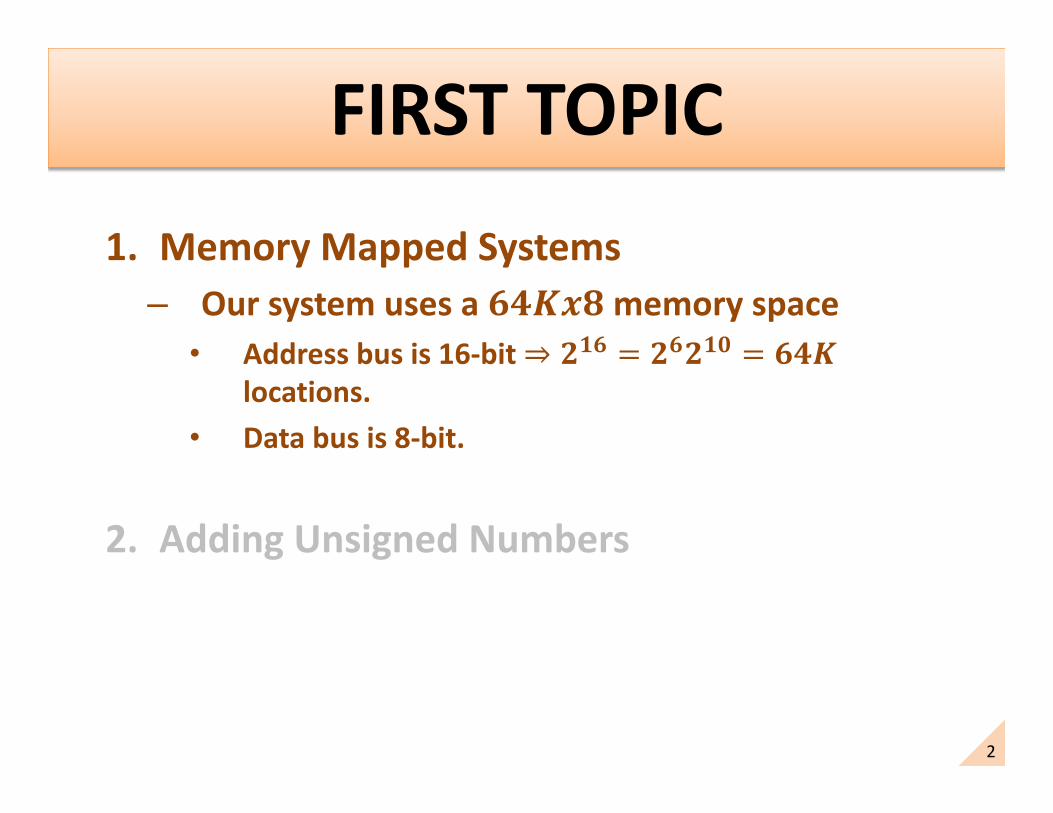
1. Memory Mapped Systems– Our system uses a memory space• Address bus is 16-bit
locations.• Data bus is 8-bit.
2. Adding Unsigned Numbers
3
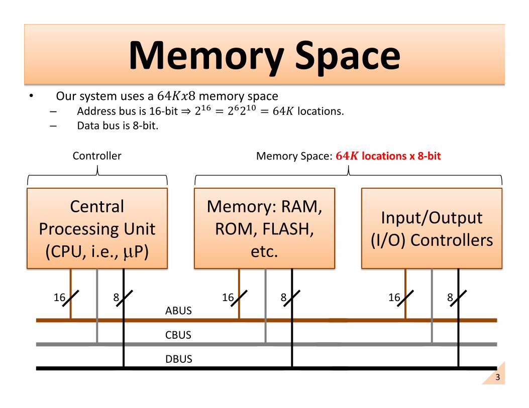
Central Processing Unit (CPU, i.e., μP)
Memory: RAM, ROM, FLASH,
etc.
Input/Output(I/O) Controllers
ABUS
CBUS
DBUS
16 1616 8 8 8
• Our system uses a memory space– Address bus is 16-bit locations.– Data bus is 8-bit.
Memory Space: locations x 8-bitController
4
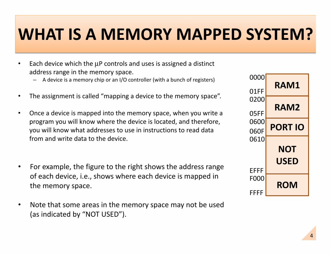
WHAT IS A MEMORY MAPPED SYSTEM?• Each device which the μP controls and uses is assigned a distinct
address range in the memory space.– A device is a memory chip or an I/O controller (with a bunch of registers)
• The assignment is called “mapping a device to the memory space”.
• Once a device is mapped into the memory space, when you write a program you will know where the device is located, and therefore, you will know what addresses to use in instructions to read data from and write data to the device.
• For example, the figure to the right shows the address range of each device, i.e., shows where each device is mapped in the memory space.
• Note that some areas in the memory space may not be used (as indicated by “NOT USED”).
RAM1
PORT IO
ROM
0000
01FF
RAM20200
05FF0600060F
NOT USED
0610
EFFFF000
FFFF
5
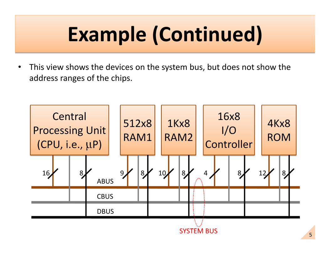
Example (Continued)• This view shows the devices on the system bus, but does not show the
address ranges of the chips.
Central Processing Unit (CPU, i.e., μP)
16x8I/O
Controller
ABUS
CBUS
DBUS
416 8
512x8 RAM1
9 8 8
SYSTEM BUS
1Kx8 RAM2
10 8
4Kx8 ROM
12 8
6
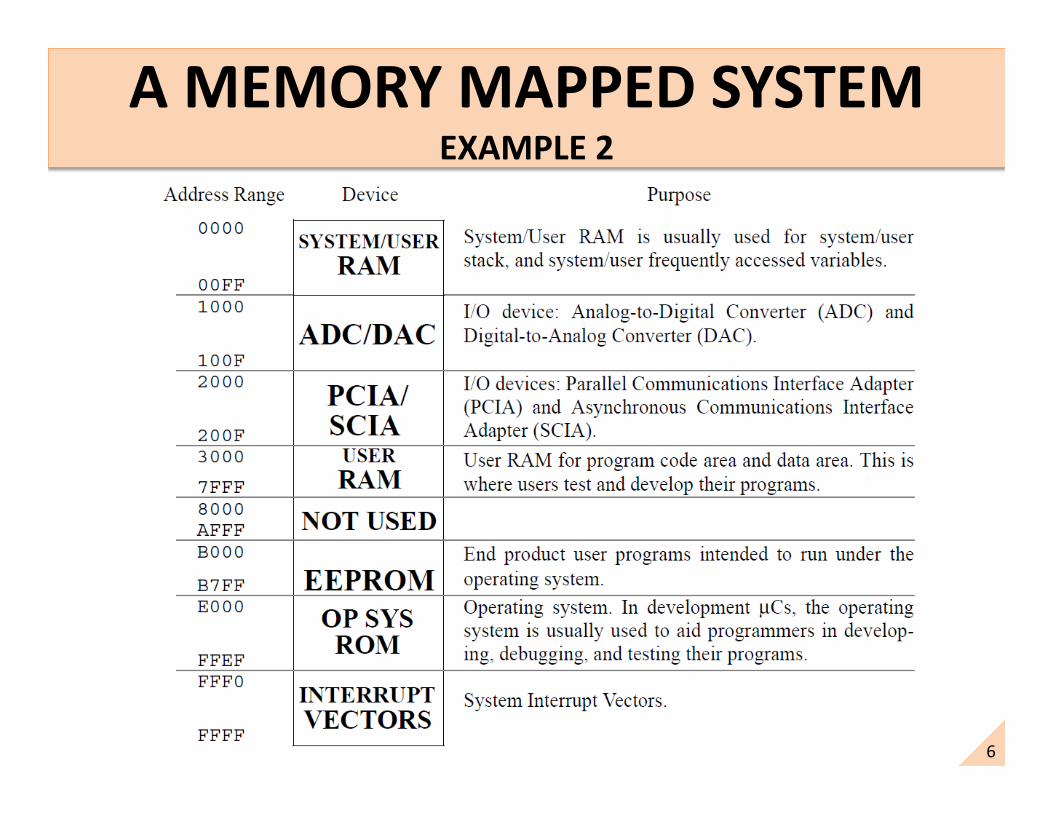
A MEMORY MAPPED SYSTEMEXAMPLE 2
7
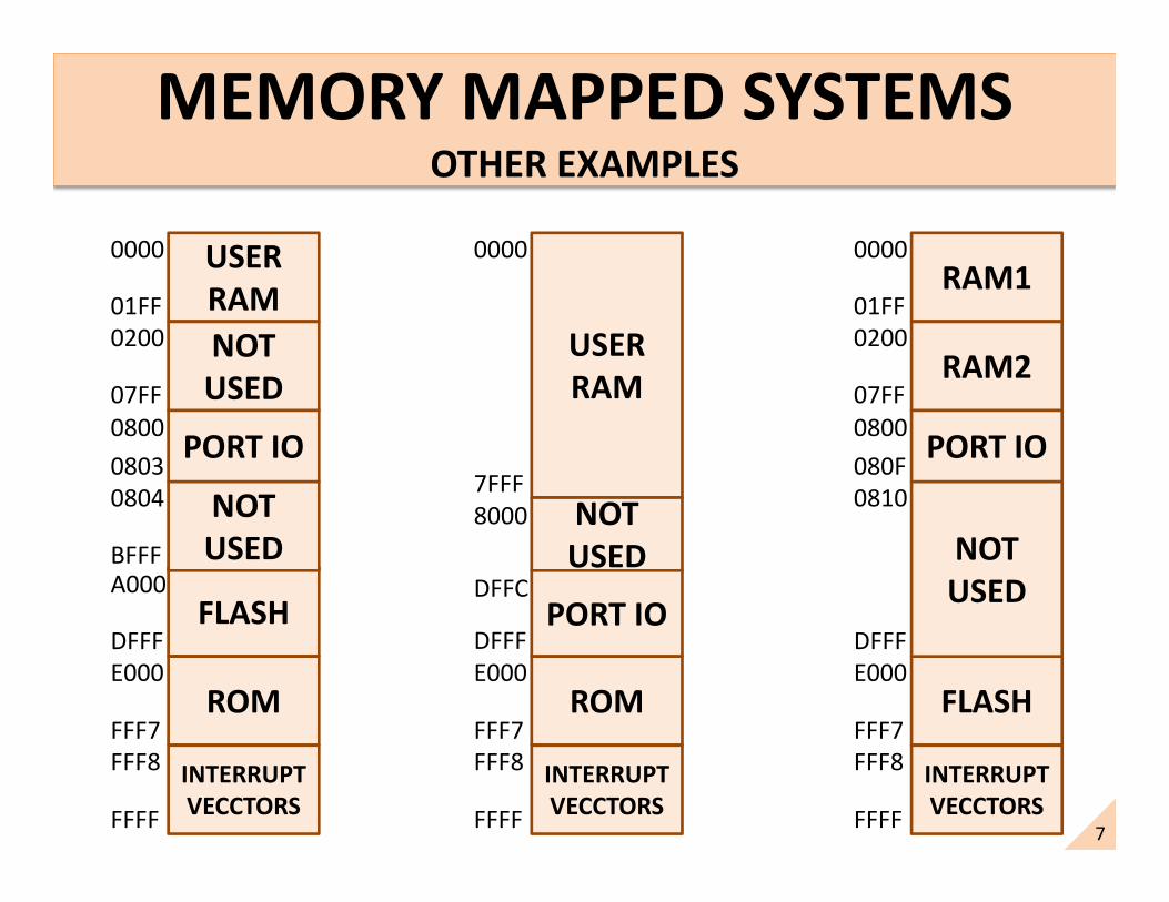
MEMORY MAPPED SYSTEMSOTHER EXAMPLES
USER RAM
PORT IO
FLASH
ROM
INTERRUPT VECCTORS
0000
01FF
NOT USED
0200
07FF08000803
A000
NOT USED
0804
BFFF
DFFFE000
FFF7FFF8
FFFF
USER RAM
ROM
INTERRUPT VECCTORS
0000
7FFFNOT USED
8000
E000
FFF7FFF8
FFFF
PORT IODFFC
DFFF
RAM1
PORT IO
FLASH
INTERRUPT VECCTORS
0000
01FF
RAM20200
07FF0800080F
NOT USED
0810
DFFFE000
FFF7FFF8
FFFF
8
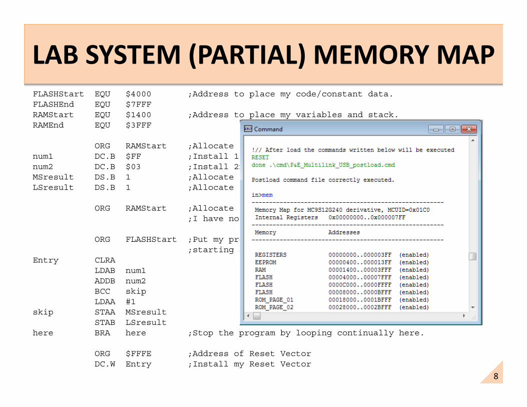
LAB SYSTEM (PARTIAL) MEMORY MAPFLASHStart EQU $4000 ;Address to place my code/constant data.FLASHEnd EQU $7FFFRAMStart EQU $1400 ;Address to place my variables and stack.RAMEnd EQU $3FFF
ORG RAMStart ;Allocate space for my variables.num1 DC.B $FF ;Install 1st number at memory location $1400num2 DC.B $03 ;Install 2nd number at memory location $1401MSresult DS.B 1 ;Allocate space to store MS Byte of result.LSresult DS.B 1 ;Allocate space to store LS Byte of result.
ORG RAMStart ;Allocate space for my stack.;I have no stack for this program.
ORG FLASHStart ;Put my program code into FLASH memory, ;starting at $4000.
Entry CLRALDAB num1ADDB num2BCC skipLDAA #1
skip STAA MSresultSTAB LSresult
here BRA here ;Stop the program by looping continually here.
ORG $FFFE ;Address of Reset VectorDC.W Entry ;Install my Reset Vector
9
SIZE AND NUMBER OF CHIPS• Amount of RAM, ROM, FLASH, and other memories
depend on the application.
– A home security system may need a small amount of RAM, ROM, and a few locations for IO controllers.
– A sound recording system and data logging application may need large amount of RAM, small ROM (program), and a few locations for IO controllers.
– You will find that the course projects for this course each need a different amount and type of memory chips.
10
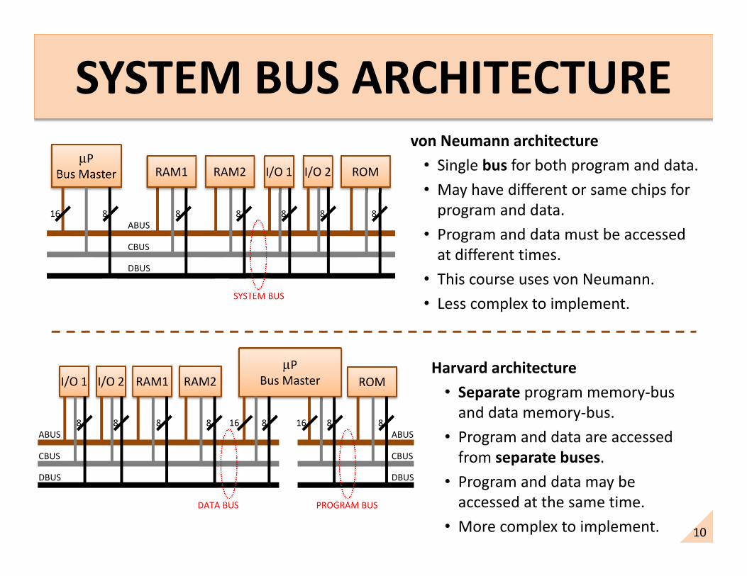
SYSTEM BUS ARCHITECTUREvon Neumann architecture• Single bus for both program and data.• May have different or same chips for
program and data.• Program and data must be accessed
at different times.• This course uses von Neumann.• Less complex to implement.
μPBus Master
ABUS
CBUS
DBUS
16 8
SYSTEM BUS
8 8 88
RAM2RAM1 ROMI/O 1 I/O 2
8
Harvard architecture• Separate program memory-bus
and data memory-bus.• Program and data are accessed
from separate buses.• Program and data may be
accessed at the same time.• More complex to implement.
ABUS
CBUS
DBUS
16 8
PROGRAM BUS
μPBus Master ROM
8ABUS
CBUS
DBUS
DATA BUS
RAM2
8
RAM1
8
I/O 1
8
I/O 2
8 16 8
11
WHERE ARE PROGRAM INSTRUCTIONS STORED?
• A ROM chip is generally used to store the initial program (aka reset routine) to be run on the microprocessor– Examples: EEPROM, FLASH, PROM.– Program needs to be preserved when power is shut off.
• When developing microprocessing applications, program instructions are sometimes stored in RAM to facilitate development, debugging, and testing.
• Once fully developed, debugged, and tested, the program will be burnt into a ROM chip, located in the memory map.
12
1. Memory Mapped Systems2. Adding Unsigned Numbers
13
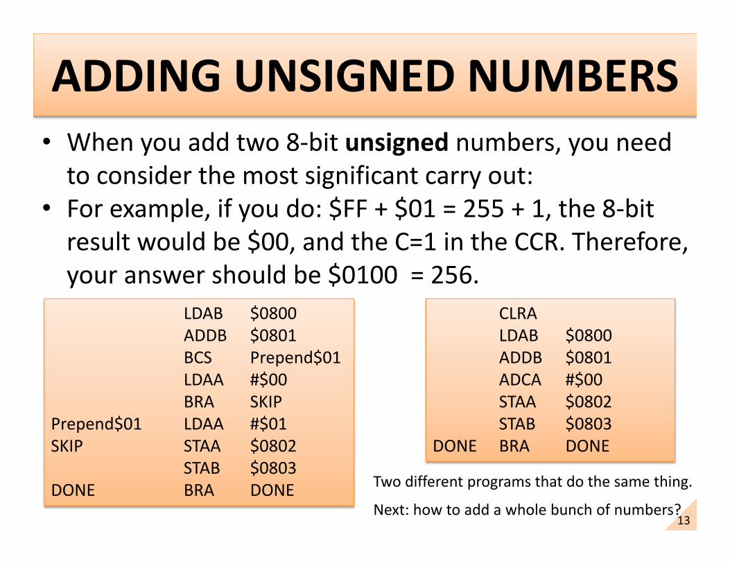
ADDING UNSIGNED NUMBERS• When you add two 8-bit unsigned numbers, you need
to consider the most significant carry out:• For example, if you do: $FF + $01 = 255 + 1, the 8-bit
result would be $00, and the C=1 in the CCR. Therefore, your answer should be $0100 = 256.
LDAB $0800ADDB $0801BCS Prepend$01LDAA #$00BRA SKIP
Prepend$01 LDAA #$01SKIP STAA $0802
STAB $0803DONE BRA DONE
CLRALDAB $0800ADDB $0801ADCA #$00STAA $0802STAB $0803
DONE BRA DONE
Two different programs that do the same thing.
Next: how to add a whole bunch of numbers?
14
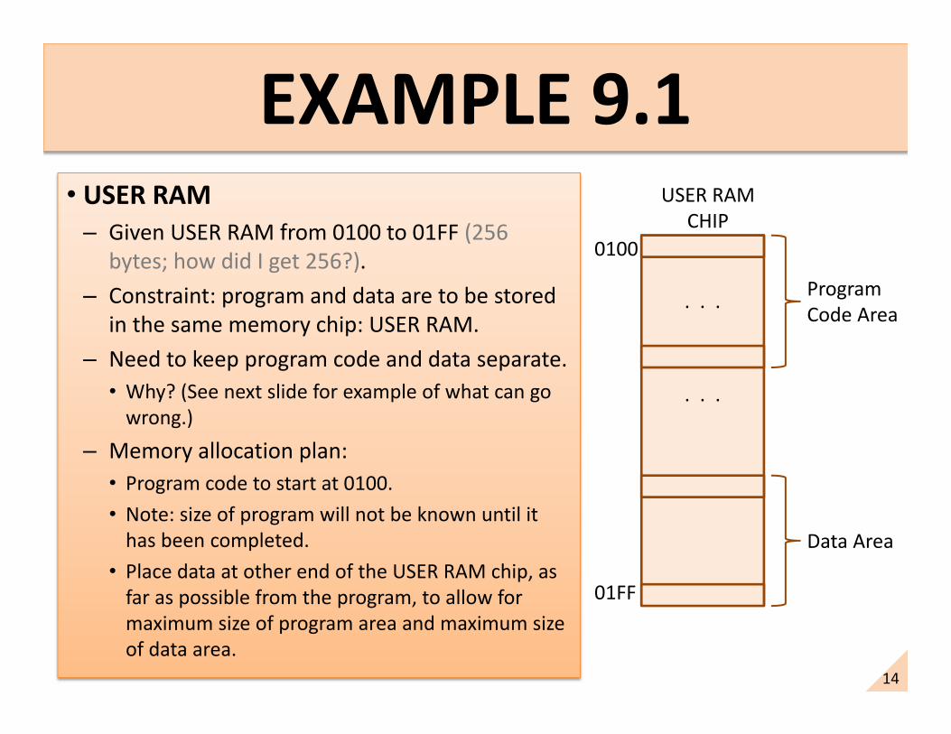
• USER RAM– Given USER RAM from 0100 to 01FF (256
bytes; how did I get 256?).– Constraint: program and data are to be stored
in the same memory chip: USER RAM.– Need to keep program code and data separate.• Why? (See next slide for example of what can go
wrong.)– Memory allocation plan:• Program code to start at 0100.• Note: size of program will not be known until it
has been completed.• Place data at other end of the USER RAM chip, as
far as possible from the program, to allow for maximum size of program area and maximum size of data area.
0100
01FF
ProgramCode Area
Data Area
. . .
. . .
USER RAM CHIP
15
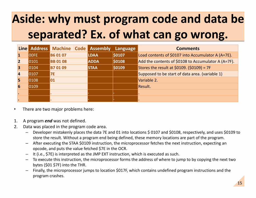
Aside: why must program code and data be separated? Ex. of what can go wrong.
Line Address Machine Code Assembly Language Comments1 00FE B6 01 07 LDAA $0107 Load contents of $0107 into Accumulator A (A=7E).2 0101 BB 01 08 ADDA $0108 Add the contents of $0108 to Accumulator A (A=7F).3 0104 B7 01 09 STAA $0109 Stores the result at $0109. ($0109) = 7F4 0107 7E Supposed to be start of data area. (variable 1)5 0108 01 Variable 2.6 0109 Result.. . . . . .. . . . . .
• There are two major problems here:
1. A program end was not defined.2. Data was placed in the program code area.
– Developer mistakenly places the data 7E and 01 into locations $ 0107 and $0108, respectively, and uses $0109 to store the result. Without a program end being defined, these memory locations are part of the program.
– After executing the STAA $0109 instruction, the microprocessor fetches the next instruction, expecting an opcode, and puts the value fetched $7E in the OCR.
– It (i.e., $7E) is interpreted as the JMP EXT instruction, which is executed as such. – To execute this instruction, the microprocessor forms the address of where to jump to by copying the next two
bytes ($01 $7F) into the THR. – Finally, the microprocessor jumps to location $017F, which contains undefined program instructions and the
program crashes.
16
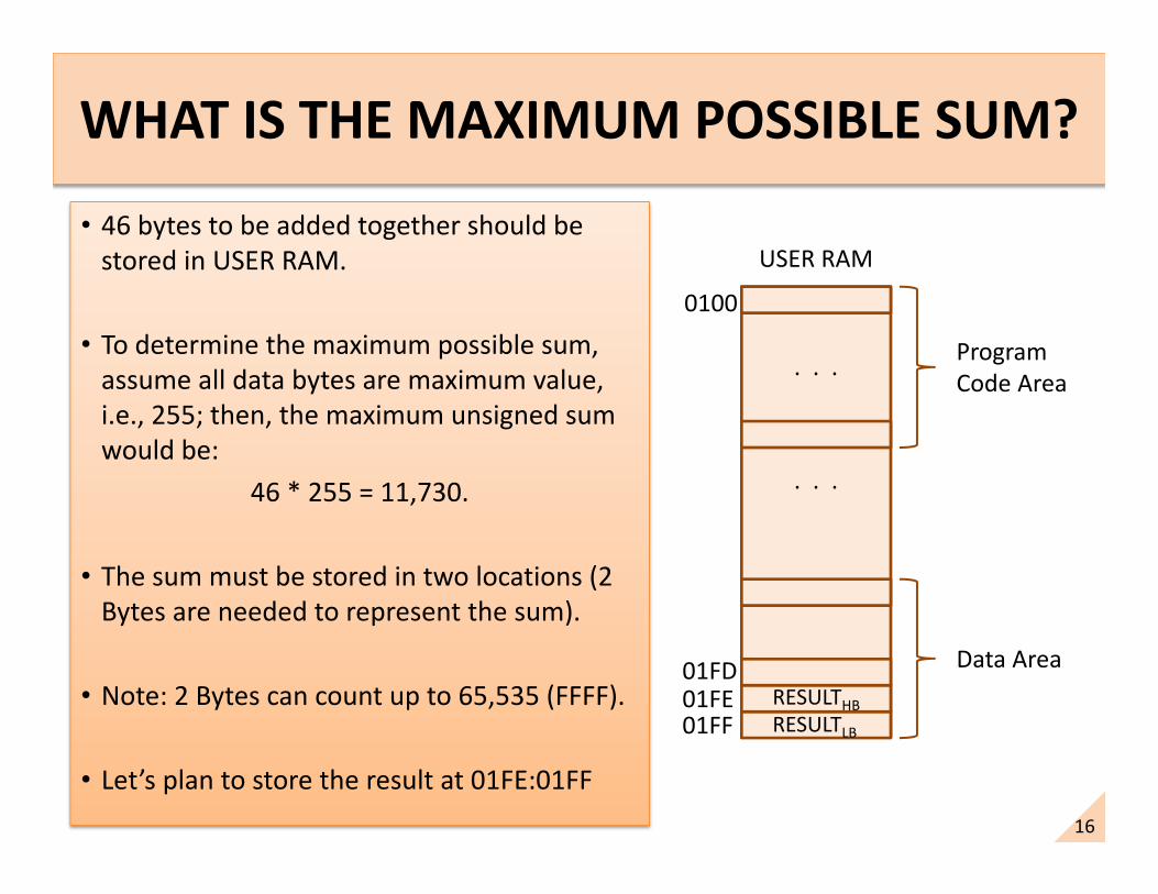
WHAT IS THE MAXIMUM POSSIBLE SUM?
• 46 bytes to be added together should be stored in USER RAM.
• To determine the maximum possible sum, assume all data bytes are maximum value, i.e., 255; then, the maximum unsigned sum would be:
46 * 255 = 11,730.
• The sum must be stored in two locations (2 Bytes are needed to represent the sum).
• Note: 2 Bytes can count up to 65,535 (FFFF).
• Let’s plan to store the result at 01FE:01FF
0100
ProgramCode Area
Data Area
. . .
. . .
01FF01FE01FD
RESULTHBRESULTLB
USER RAM
17
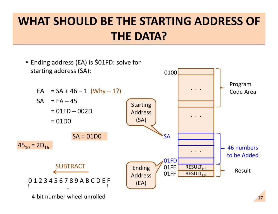
WHAT SHOULD BE THE STARTING ADDRESS OF THE DATA?
• Ending address (EA) is $01FD: solve for starting address (SA):
EA = SA + 46 – 1 (Why – 1?)SA = EA – 45
= 01FD – 002D= 01D0
0100
ProgramCode Area
46 numbers to be Added
. . .
. . .
01FF01FE01FD
RESULTHBRESULTLB
SA4510 = 2D16
Starting Address
(SA)
Ending Address
(EA)
Result
SA = 01D0
0 1 2 3 4 5 6 7 8 9 A B C D E F
SUBTRACT
4-bit number wheel unrolled
. . .
18
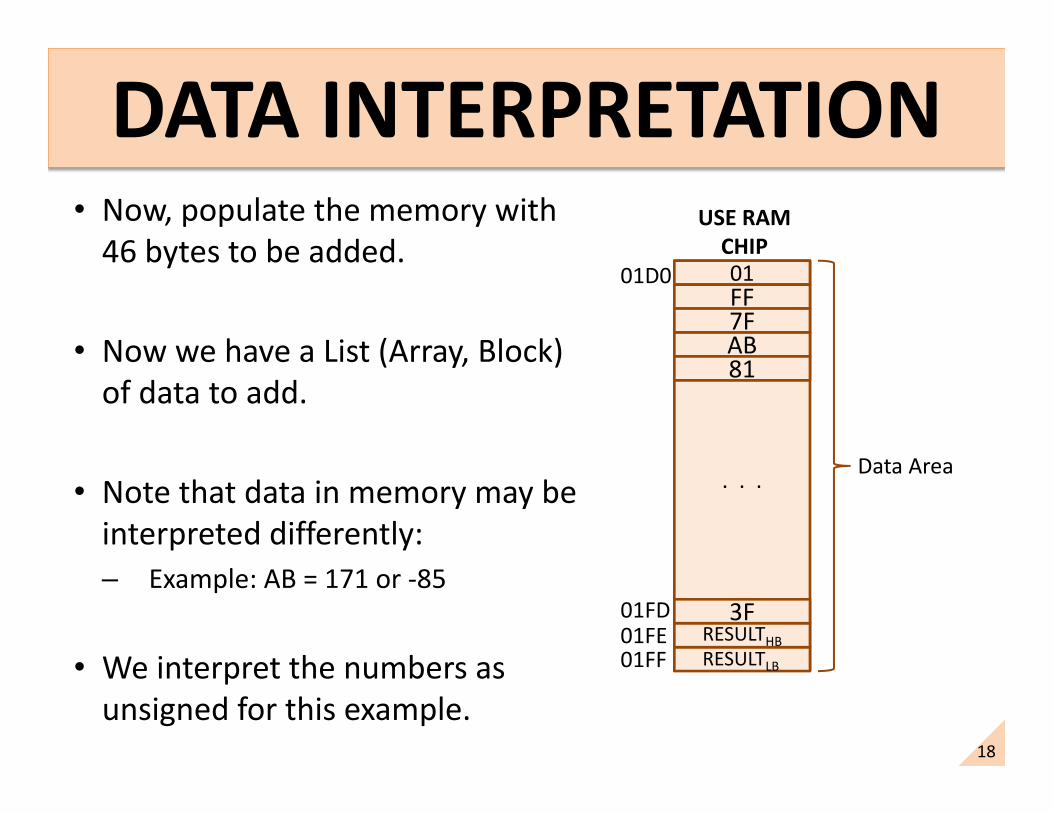
• Now, populate the memory with 46 bytes to be added.
• Now we have a List (Array, Block) of data to add.
• Note that data in memory may be interpreted differently:– Example: AB = 171 or -85
• We interpret the numbers as unsigned for this example.
01D0
01FF
Data Area
01FF
. . .
3F01FE01FD
RESULTHBRESULTLB
USE RAM CHIP
7FAB81
19
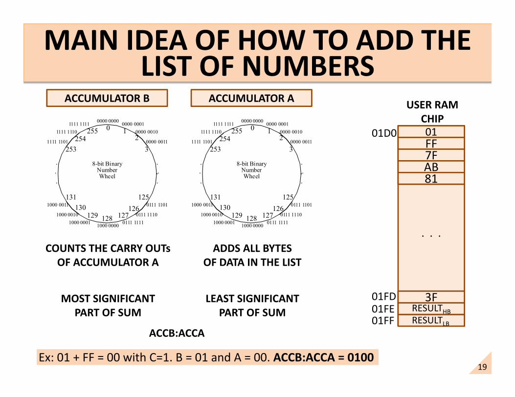
MAIN IDEA OF HOW TO ADD THE LIST OF NUMBERS
01D0
01FF
01FF
. . .
3F01FE01FD
RESULTHBRESULTLB
USER RAM CHIP
7FAB81
ACCUMULATOR B
0 12
..
255254
253 3
.
...
0000 0000
1111 1101
1111 11101111 1111
0000 0011
0000 00100000 0001
128 127126
129130
131 125
1000 0000
1000 0011
1000 00101000 0001
0111 1101
0111 11100111 1111
8-bit BinaryNumberWheel
MOST SIGNIFICANT PART OF SUM
COUNTS THE CARRY OUTsOF ACCUMULATOR A
0 12
..
255254
253 3
.
...
0000 0000
1111 1101
1111 11101111 1111
0000 0011
0000 00100000 0001
128 127126
129130
131 125
1000 0000
1000 0011
1000 00101000 0001
0111 1101
0111 11100111 1111
8-bit BinaryNumberWheel
ACCUMULATOR A
LEAST SIGNIFICANT PART OF SUM
ADDS ALL BYTESOF DATA IN THE LIST
ACCB:ACCA
Ex: 01 + FF = 00 with C=1. B = 01 and A = 00. ACCB:ACCA = 0100
20
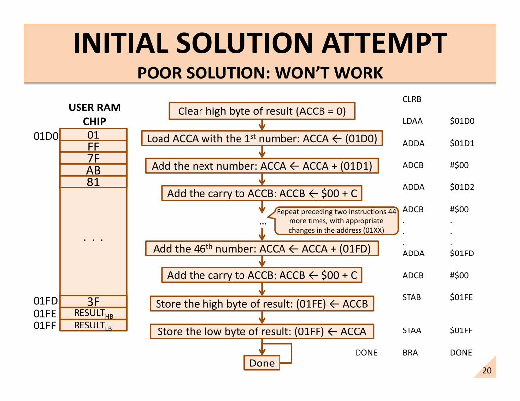
INITIAL SOLUTION ATTEMPTPOOR SOLUTION: WON’T WORK
CLRB
LDAA $01D0
ADDA $01D1
ADCB #$00
ADDA $01D2
ADCB #$00. .. .. .ADDA $01FD
ADCB #$00
STAB $01FE
STAA $01FF
DONE BRA DONE
Clear high byte of result (ACCB = 0)
Load ACCA with the 1st number: ACCA ← (01D0)
Add the next number: ACCA ← ACCA + (01D1)
Add the carry to ACCB: ACCB ← $00 + C
…
Add the 46th number: ACCA ← ACCA + (01FD)
Add the carry to ACCB: ACCB ← $00 + C
Store the high byte of result: (01FE) ← ACCB
Store the low byte of result: (01FF) ← ACCA
Done
01D0
01FF
01FF
. . .
3F01FE01FD
RESULTHBRESULTLB
USER RAM CHIP
7FAB81
Repeat preceding two instructions 44 more times, with appropriate changes in the address (01XX)
21
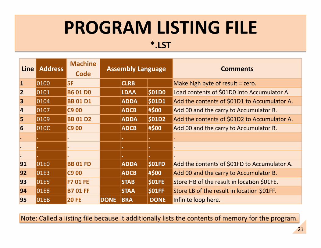
PROGRAM LISTING FILE*.LST
Line AddressMachine
CodeAssembly Language Comments
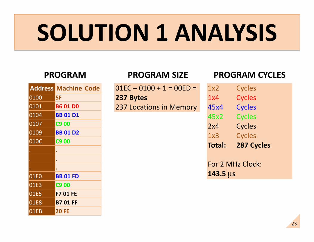
1 0100 5F CLRB Make high byte of result = zero.2 0101 B6 01 D0 LDAA $01D0 Load contents of $01D0 into Accumulator A.3 0104 BB 01 D1 ADDA $01D1 Add the contents of $01D1 to Accumulator A.4 0107 C9 00 ADCB #$00 Add 00 and the carry to Accumulator B.5 0109 BB 01 D2 ADDA $01D2 Add the contents of $01D2 to Accumulator A.6 010C C9 00 ADCB #$00 Add 00 and the carry to Accumulator B.. . . . . .. . . . . .. . . . . .91 01E0 BB 01 FD ADDA $01FD Add the contents of $01FD to Accumulator A.92 01E3 C9 00 ADCB #$00 Add 00 and the carry to Accumulator B.93 01E5 F7 01 FE STAB $01FE Store HB of the result in location $01FE.94 01E8 B7 01 FF STAA $01FF Store LB of the result in location $01FF.95 01EB 20 FE DONE BRA DONE Infinite loop here.
Note: Called a listing file because it additionally lists the contents of memory for the program.
22
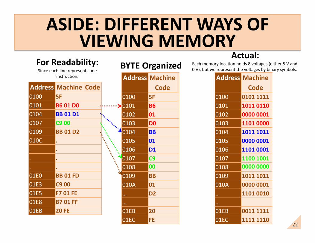
ASIDE: DIFFERENT WAYS OF VIEWING MEMORY
Address Machine Code0100 5F0101 B6 01 D00104 BB 01 D10107 C9 000109 BB 01 D2010C .. .. .. .01E0 BB 01 FD01E3 C9 0001E5 F7 01 FE01E8 B7 01 FF01EB 20 FE
Address MachineCode
0100 5F0101 B60102 010103 D00104 BB0105 010106 D10107 C90108 000109 BB010A 01… D2…01EB 2001EC FE
For Readability:Since each line represents one
instruction.
BYTE OrganizedAddress Machine
Code0100 0101 11110101 1011 01100102 0000 00010103 1101 00000104 1011 10110105 0000 00010106 1101 00010107 1100 10010108 0000 00000109 1011 1011010A 0000 0001… 1101 0010…01EB 0011 111101EC 1111 1110
Actual:Each memory location holds 8 voltages (either 5 V and 0 V), but we represent the voltages by binary symbols.
23
Address Machine Code0100 5F0101 B6 01 D00104 BB 01 D10107 C9 000109 BB 01 D2010C C9 00. .. .. .01E0 BB 01 FD01E3 C9 0001E5 F7 01 FE01E8 B7 01 FF01EB 20 FE
PROGRAM01EC – 0100 + 1 = 00ED = 237 Bytes237 Locations in Memory
PROGRAM SIZE1x2 Cycles1x4 Cycles45x4 Cycles45x2 Cycles2x4 Cycles1x3 CyclesTotal: 287 Cycles
For 2 MHz Clock:143.5 μs
PROGRAM CYCLES
24
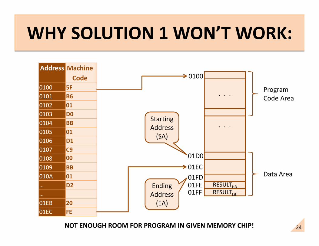
WHY SOLUTION 1 WON’T WORK:
Address MachineCode
0100 5F0101 B60102 010103 D00104 BB0105 010106 D10107 C90108 000109 BB010A 01… D2…01EB 2001EC FE
0100
ProgramCode Area
Data Area
. . .
. . .
01FF01FE01FD
RESULTHBRESULTLB
01D0
Starting Address
(SA)
Ending Address
(EA)
01EC
NOT ENOUGH ROOM FOR PROGRAM IN GIVEN MEMORY CHIP!
25
01D0
01FF
01FF
. . .
3F01FE01FD
RESULTHBRESULTLB
USER RAM CHIP
7FAB81
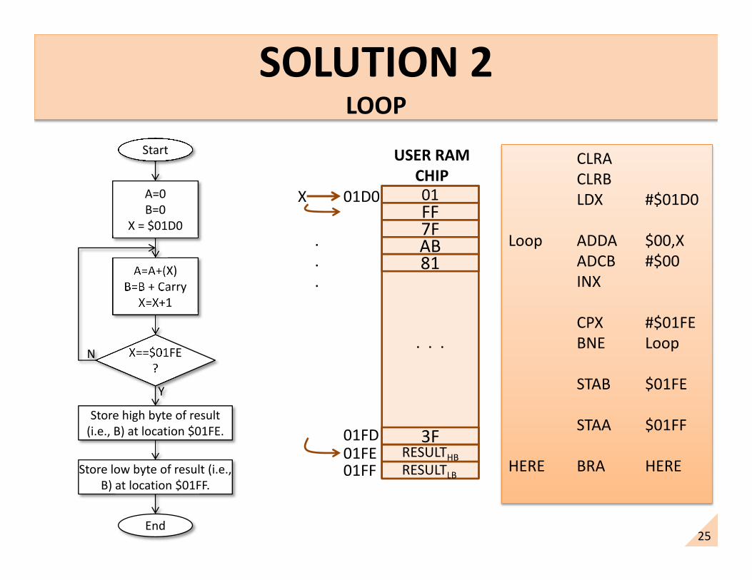
SOLUTION 2LOOP
CLRACLRBLDX #$01D0
Loop ADDA $00,XADCB #$00INX
CPX #$01FEBNE Loop
STAB $01FE
STAA $01FF
HERE BRA HERE
X
.
.
.
Start
A=0B=0
X = $01D0
A=A+(X)B=B + Carry
X=X+1
X==$01FE?
Store low byte of result (i.e., B) at location $01FF.
End
N
Store high byte of result (i.e., B) at location $01FE.
Y
26
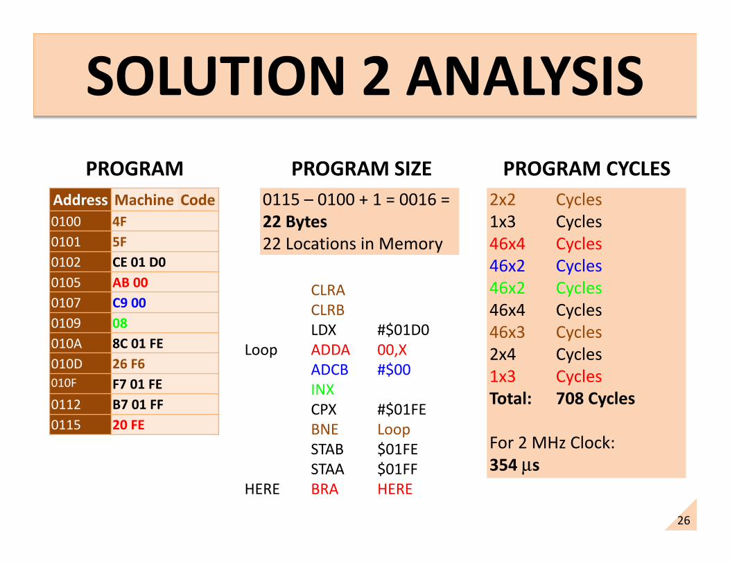
Address Machine Code0100 4F0101 5F0102 CE 01 D00105 AB 000107 C9 000109 08010A 8C 01 FE010D 26 F6010F F7 01 FE0112 B7 01 FF0115 20 FE
PROGRAM0115 – 0100 + 1 = 0016 = 22 Bytes22 Locations in Memory
PROGRAM SIZE2x2 Cycles1x3 Cycles46x4 Cycles46x2 Cycles46x2 Cycles46x4 Cycles46x3 Cycles2x4 Cycles1x3 CyclesTotal: 708 Cycles
For 2 MHz Clock:354 μs
PROGRAM CYCLES
CLRACLRBLDX #$01D0
Loop ADDA 00,XADCB #$00INXCPX #$01FEBNE LoopSTAB $01FESTAA $01FF
HERE BRA HERE
27
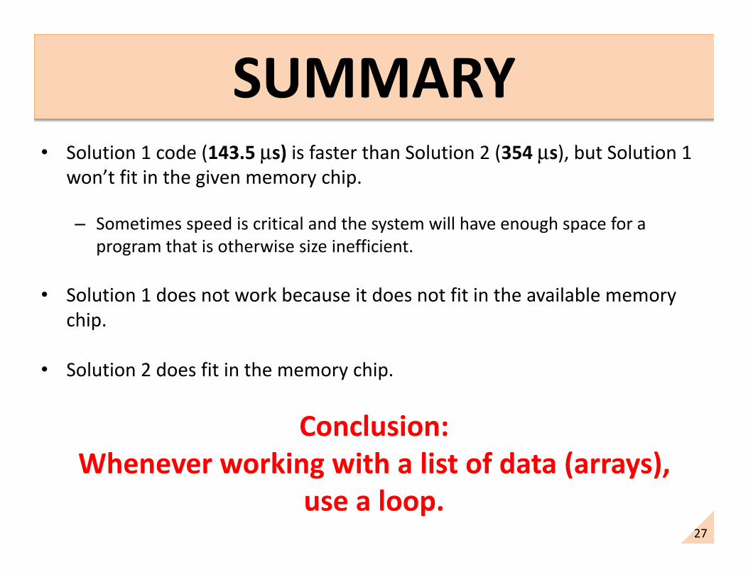
• Solution 1 code (143.5 μs) is faster than Solution 2 (354 μs), but Solution 1 won’t fit in the given memory chip.
– Sometimes speed is critical and the system will have enough space for a program that is otherwise size inefficient.
• Solution 1 does not work because it does not fit in the available memory chip.
• Solution 2 does fit in the memory chip.
Conclusion:Whenever working with a list of data (arrays),
use a loop.