EFM32 Tiny Gecko Family EM2 – Deep Sleep EM3 - Stop EM4 ... · EM0 - Active EM1 - Sleep EM2 –...
203
EFM32 Tiny Gecko Family EFM32TG Data Sheet The EFM32 Tiny Gecko MCUs are the world’s most energy-friend- ly microcontrollers. The EFM32TG offers unmatched performance and ultra low power consumption in both active and sleep modes. EFM32TG devices consume as little as 0.6 μA in Stop mode and 150 μA/MHz in Run mode. It also features autonomous peripherals, high overall chip and analog integration, and the performance of the industry standard 32-bit ARM Cortex- M3 processor, making it perfect for battery-powered systems and systems with high-per- formance, low-energy requirements. EFM32TG applications include the following: KEY FEATURES • ARM Cortex-M3 at 32 MHz • Ultra low power operation • 0.6 μA current in Stop (EM3), with brown-out detection and RAM retention • 51 μA/MHz in EM1 • 150 μA/MHz in Run mode (EM0) • Fast wake-up time of 2 µs • Hardware cryptography (AES) • Up to 32 kB of Flash and 4 kB of RAM • Smart metering • Water metering • Gas metering • Industrial and home automation • Alarm and security systems • Health and fitness applications 32-bit bus Lowest power mode with peripheral operational: EM2 – Deep Sleep EM1 - Sleep EM4 - Shutoff EM0 - Active EM3 - Stop Core / Memory Flash Program Memory RAM Memory ARM Cortex TM M3 processor Debug Interface DMA Controller Security Hardware AES Energy Management Power-on Reset Voltage Regulator Voltage Comparator Brown-out Detector Clock Management High Frequency RC Oscillator Low Freq. RC Oscillator Low Frequency Crystal Oscillator Watchdog Oscillator Auxiliary High Freq. RC Osc. High Frequency Crystal Oscillator Analog Interfaces DAC ADC Operational Amplifier Analog Comparator Peripheral Reflex System Serial Interfaces I 2 C I/O Ports Timers and Triggers Timer/Counter Low Energy Timer Real Time Counter External Interrupts General Purpose I/O LESENSE Pulse Counter USART Low Energy UART TM Pin Reset Watchdog Timer LCD Controller silabs.com | Building a more connected world. Rev. 2.00
Transcript of EFM32 Tiny Gecko Family EM2 – Deep Sleep EM3 - Stop EM4 ... · EM0 - Active EM1 - Sleep EM2 –...
EFM32 Tiny Gecko FamilyEFM32TG Data Sheet
The EFM32 Tiny Gecko MCUs are the world’s most energy-friend-ly microcontrollers.The EFM32TG offers unmatched performance and ultra low power consumption in bothactive and sleep modes. EFM32TG devices consume as little as 0.6 μA in Stop modeand 150 μA/MHz in Run mode. It also features autonomous peripherals, high overall chipand analog integration, and the performance of the industry standard 32-bit ARM Cortex-M3 processor, making it perfect for battery-powered systems and systems with high-per-formance, low-energy requirements.
EFM32TG applications include the following:
KEY FEATURES
• ARM Cortex-M3 at 32 MHz• Ultra low power operation
• 0.6 μA current in Stop (EM3), withbrown-out detection and RAM retention
• 51 μA/MHz in EM1• 150 μA/MHz in Run mode (EM0)
• Fast wake-up time of 2 µs• Hardware cryptography (AES)• Up to 32 kB of Flash and 4 kB of RAM• Smart metering
• Water metering• Gas metering
• Industrial and home automation• Alarm and security systems• Health and fitness applications
32-bit bus
Lowest power mode with peripheral operational:
EM2 – Deep SleepEM1 - Sleep EM4 - ShutoffEM0 - Active EM3 - Stop
Core / Memory
Flash Program Memory
RAM Memory
ARM CortexTM M3 processor
Debug Interface
DMA Controller
Security
Hardware AES
Energy Management
Power-on Reset
Voltage Regulator
Voltage Comparator
Brown-out Detector
Clock Management
High Frequency RC Oscillator
Low Freq. RC Oscillator
Low FrequencyCrystal Oscillator
Watchdog Oscillator
Auxiliary High Freq. RC Osc.
High Frequency Crystal Oscillator
Analog Interfaces
DACADC
Operational Amplifier
Analog Comparator
Peripheral Reflex System
Serial Interfaces
I2C
I/O Ports Timers and Triggers
Timer/Counter
Low Energy Timer Real Time Counter
External Interrupts
General Purpose I/O
LESENSE
Pulse Counter
USART
Low Energy UARTTM Pin Reset
Watchdog Timer LCD Controller
silabs.com | Building a more connected world. Rev. 2.00
1. Feature List
• ARM Cortex-M3 CPU platform• High Performance 32-bit processor @ up to 32 MHz• Wake-up Interrupt Controller
• Flexible Energy Management System• 20 nA @ 3 V Shutoff Mode• 0.6 µA @ 3 V Stop Mode, including Power-on Reset, Brown-out Detector, RAM and CPU retention• 1.0 µA @ 3 V Deep Sleep Mode, including RTC with 32.768 kHz oscillator, Power-on Reset, Brown-out Detector, RAM and CPU
retention• 51 µA/MHz @ 3 V Sleep Mode• 150 µA/MHz @ 3 V Run Mode, with code executed from flash
• 32/16/8 KB Flash• 4/2 KB RAM• Up to 56 General Purpose I/O pins
• Configurable push-pull, open-drain, pull-up/down, input filter, drive strength• Configurable peripheral I/O locations• 16 asynchronous external interrupts• Output state retention and wake-up from Shutoff Mode
• 8 Channel DMA Controller• 8 Channel Peripheral Reflex System (PRS) for autonomous inter- peripheral signaling• Hardware AES with 128/256-bit keys in 54/75 cycles• Timers/Counters
• 2× 16-bit Timer/Counter• 2×3 Compare/Capture/PWM channels
• 16-bit Low Energy Timer• 1× 24-bit Real-Time Counter• 1× 16-bit Pulse Counter• Watchdog Timer with dedicated RC oscillator @ 50 nA
• Integrated LCD Controller for up to 8×20 segments• Voltage boost, adjustable contrast and autonomous animation
• Communication interfaces• Up to 2× Universal Synchronous/Asynchronous Receiver/ Transmitter
• UART/SPI/SmartCard (ISO 7816)/IrDA/I2S• Low Energy UART
• Autonomous operation with DMA in Deep Sleep Mode• I2C Interface with SMBus support
• Address recognition in Stop Mode• Ultra low power precision analog peripherals
• 12-bit 1 Msamples/s Analog to Digital Converter• 8 single ended channels/4 differential channels• On-chip temperature sensor
• 12-bit 500 ksamples/s Digital to Analog Converter• Up to 2× Analog Comparator
• Capacitive sensing with up to 8 inputs• 3× Operational Amplifier
• 6.1 MHz GBW, Rail-to-rail, Programmable Gain• Supply Voltage Comparator
• Low Energy Sensor Interface (LESENSE)• Autonomous sensor monitoring in Deep Sleep Mode• Wide range of sensors supported, including LC sensors and capacitive buttons
• Ultra efficient Power-on Reset and Brown-Out Detector• 2-pin Serial Wire Debug interface
EFM32TG Data SheetFeature List
silabs.com | Building a more connected world. Rev. 2.00 | 2
• 1-pin Serial Wire Viewer• Pre-Programmed UART Bootloader• Temperature range -40 to 85 ºC• Single power supply 1.98 to 3.8 V• Packages:
• BGA48• QFN24• QFN32• QFN64• TQFP48• TQFP64
EFM32TG Data SheetFeature List
silabs.com | Building a more connected world. Rev. 2.00 | 3
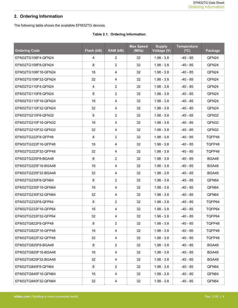
2. Ordering Information
The following table shows the available EFM32TG devices.
Table 2.1. Ordering Information
Ordering Code Flash (kB) RAM (kB)Max Speed
(MHz)Supply
Voltage (V)Temperature
(ºC) Package
EFM32TG108F4-QFN24 4 2 32 1.98 - 3.8 -40 - 85 QFN24
EFM32TG108F8-QFN24 8 2 32 1.98 - 3.8 -40 - 85 QFN24
EFM32TG108F16-QFN24 16 4 32 1.98 - 3.8 -40 - 85 QFN24
EFM32TG108F32-QFN24 32 4 32 1.98 - 3.8 -40 - 85 QFN24
EFM32TG110F4-QFN24 4 2 32 1.98 - 3.8 -40 - 85 QFN24
EFM32TG110F8-QFN24 8 2 32 1.98 - 3.8 -40 - 85 QFN24
EFM32TG110F16-QFN24 16 4 32 1.98 - 3.8 -40 - 85 QFN24
EFM32TG110F32-QFN24 32 4 32 1.98 - 3.8 -40 - 85 QFN24
EFM32TG210F8-QFN32 8 2 32 1.98 - 3.8 -40 - 85 QFN32
EFM32TG210F16-QFN32 16 4 32 1.98 - 3.8 -40 - 85 QFN32
EFM32TG210F32-QFN32 32 4 32 1.98 - 3.8 -40 - 85 QFN32
EFM32TG222F8-QFP48 8 2 32 1.98 - 3.8 -40 - 85 TQFP48
EFM32TG222F16-QFP48 16 4 32 1.98 - 3.8 -40 - 85 TQFP48
EFM32TG222F32-QFP48 32 4 32 1.98 - 3.8 -40 - 85 TQFP48
EFM32TG225F8-BGA48 8 2 32 1.98 - 3.8 -40 - 85 BGA48
EFM32TG225F16-BGA48 16 4 32 1.98 - 3.8 -40 - 85 BGA48
EFM32TG225F32-BGA48 32 4 32 1.98 - 3.8 -40 - 85 BGA48
EFM32TG230F8-QFN64 8 2 32 1.98 - 3.8 -40 - 85 QFN64
EFM32TG230F16-QFN64 16 4 32 1.98 - 3.8 -40 - 85 QFN64
EFM32TG230F32-QFN64 32 4 32 1.98 - 3.8 -40 - 85 QFN64
EFM32TG232F8-QFP64 8 2 32 1.98 - 3.8 -40 - 85 TQFP64
EFM32TG232F16-QFP64 16 4 32 1.98 - 3.8 -40 - 85 TQFP64
EFM32TG232F32-QFP64 32 4 32 1.98 - 3.8 -40 - 85 TQFP64
EFM32TG822F8-QFP48 8 2 32 1.98 - 3.8 -40 - 85 TQFP48
EFM32TG822F16-QFP48 16 4 32 1.98 - 3.8 -40 - 85 TQFP48
EFM32TG822F32-QFP48 32 4 32 1.98 - 3.8 -40 - 85 TQFP48
EFM32TG825F8-BGA48 8 2 32 1.98 - 3.8 -40 - 85 BGA48
EFM32TG825F16-BGA48 16 4 32 1.98 - 3.8 -40 - 85 BGA48
EFM32TG825F32-BGA48 32 4 32 1.98 - 3.8 -40 - 85 BGA48
EFM32TG840F8-QFN64 8 2 32 1.98 - 3.8 -40 - 85 QFN64
EFM32TG840F16-QFN64 16 4 32 1.98 - 3.8 -40 - 85 QFN64
EFM32TG840F32-QFN64 32 4 32 1.98 - 3.8 -40 - 85 QFN64
EFM32TG Data SheetOrdering Information
silabs.com | Building a more connected world. Rev. 2.00 | 4
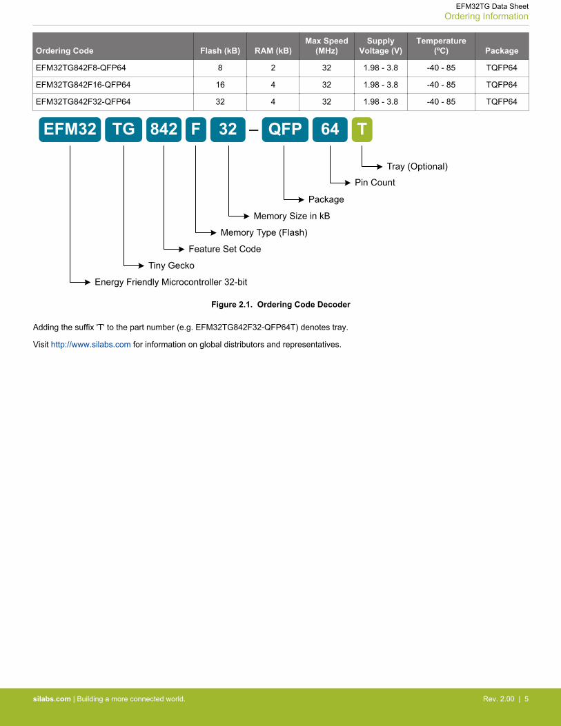
Ordering Code Flash (kB) RAM (kB)Max Speed
(MHz)Supply
Voltage (V)Temperature
(ºC) Package
EFM32TG842F8-QFP64 8 2 32 1.98 - 3.8 -40 - 85 TQFP64
EFM32TG842F16-QFP64 16 4 32 1.98 - 3.8 -40 - 85 TQFP64
EFM32TG842F32-QFP64 32 4 32 1.98 - 3.8 -40 - 85 TQFP64
EFM32 TG 842 32F QFP 64 T
Tray (Optional)
Pin Count
Package
Memory Size in kB
Memory Type (Flash)
Feature Set Code
Tiny Gecko
Energy Friendly Microcontroller 32-bit
–
Figure 2.1. Ordering Code Decoder
Adding the suffix 'T' to the part number (e.g. EFM32TG842F32-QFP64T) denotes tray.
Visit http://www.silabs.com for information on global distributors and representatives.
EFM32TG Data SheetOrdering Information
silabs.com | Building a more connected world. Rev. 2.00 | 5
Table of Contents1. Feature List . . . . . . . . . . . . . . . . . . . . . . . . . . . . . . . . 2
2. Ordering Information . . . . . . . . . . . . . . . . . . . . . . . . . . . . 4
3. System Summary . . . . . . . . . . . . . . . . . . . . . . . . . . . . . 113.1 System Introduction . . . . . . . . . . . . . . . . . . . . . . . . . . . .11
3.1.1 ARM Cortex-M3 Core . . . . . . . . . . . . . . . . . . . . . . . . .113.1.2 Debug Interface (DBG) . . . . . . . . . . . . . . . . . . . . . . . . .113.1.3 Memory System Controller (MSC) . . . . . . . . . . . . . . . . . . . . .113.1.4 Direct Memory Access Controller (DMA) . . . . . . . . . . . . . . . . . . .123.1.5 Reset Management Unit (RMU) . . . . . . . . . . . . . . . . . . . . . .123.1.6 Energy Management Unit (EMU) . . . . . . . . . . . . . . . . . . . . .123.1.7 Clock Management Unit (CMU) . . . . . . . . . . . . . . . . . . . . . .123.1.8 Watchdog (WDOG) . . . . . . . . . . . . . . . . . . . . . . . . . .123.1.9 Peripheral Reflex System (PRS) . . . . . . . . . . . . . . . . . . . . .123.1.10 Inter-Integrated Circuit Interface (I2C) . . . . . . . . . . . . . . . . . . .123.1.11 Universal Synchronous/Asynchronous Receiver/Transmitter (USART) . . . . . . . .123.1.12 Pre-Programmed UART Bootloader . . . . . . . . . . . . . . . . . . . .123.1.13 Low Energy Universal Asynchronous Receiver/Transmitter (LEUART) . . . . . . . .123.1.14 Timer/Counter (TIMER) . . . . . . . . . . . . . . . . . . . . . . . .133.1.15 Real Time Counter (RTC) . . . . . . . . . . . . . . . . . . . . . . .133.1.16 Low Energy Timer (LETIMER) . . . . . . . . . . . . . . . . . . . . . .133.1.17 Pulse Counter (PCNT) . . . . . . . . . . . . . . . . . . . . . . . .133.1.18 Analog Comparator (ACMP) . . . . . . . . . . . . . . . . . . . . . .133.1.19 Voltage Comparator (VCMP) . . . . . . . . . . . . . . . . . . . . . .133.1.20 Analog to Digital Converter (ADC) . . . . . . . . . . . . . . . . . . . .133.1.21 Digital to Analog Converter (DAC) . . . . . . . . . . . . . . . . . . . .133.1.22 Operational Amplifier (OPAMP) . . . . . . . . . . . . . . . . . . . . .133.1.23 Low Energy Sensor Interface (LESENSE) . . . . . . . . . . . . . . . . . .133.1.24 Advanced Encryption Standard Accelerator (AES) . . . . . . . . . . . . . . .143.1.25 General Purpose Input/Output (GPIO) . . . . . . . . . . . . . . . . . . .143.1.26 Liquid Crystal Display Driver (LCD) . . . . . . . . . . . . . . . . . . . .14
3.2 Configuration Summary . . . . . . . . . . . . . . . . . . . . . . . . . .153.2.1 EFM32TG108 . . . . . . . . . . . . . . . . . . . . . . . . . . . .153.2.2 EFM32TG110 . . . . . . . . . . . . . . . . . . . . . . . . . . . .163.2.3 EFM32TG210 . . . . . . . . . . . . . . . . . . . . . . . . . . . .173.2.4 EFM32TG222 . . . . . . . . . . . . . . . . . . . . . . . . . . . .183.2.5 EFM32TG225 . . . . . . . . . . . . . . . . . . . . . . . . . . . .193.2.6 EFM32TG230 . . . . . . . . . . . . . . . . . . . . . . . . . . . .203.2.7 EFM32TG232 . . . . . . . . . . . . . . . . . . . . . . . . . . . .213.2.8 EFM32TG822 . . . . . . . . . . . . . . . . . . . . . . . . . . . .223.2.9 EFM32TG825 . . . . . . . . . . . . . . . . . . . . . . . . . . . .233.2.10 EFM32TG840 . . . . . . . . . . . . . . . . . . . . . . . . . . .243.2.11 EFM32TG842 . . . . . . . . . . . . . . . . . . . . . . . . . . .25
3.3 Memory Map . . . . . . . . . . . . . . . . . . . . . . . . . . . . . .26
4. Electrical Characteristics . . . . . . . . . . . . . . . . . . . . . . . . . . 28
silabs.com | Building a more connected world. Rev. 2.00 | 6
4.1 Test Conditions . . . . . . . . . . . . . . . . . . . . . . . . . . . . .284.1.1 Typical Values . . . . . . . . . . . . . . . . . . . . . . . . . . .284.1.2 Minimum and Maximum Values . . . . . . . . . . . . . . . . . . . . . .28
4.2 Absolute Maximum Ratings . . . . . . . . . . . . . . . . . . . . . . . . .28
4.3 General Operating Conditions . . . . . . . . . . . . . . . . . . . . . . . .28
4.4 Current Consumption . . . . . . . . . . . . . . . . . . . . . . . . . . .294.4.1 EM2 Current Consumption . . . . . . . . . . . . . . . . . . . . . . .304.4.2 EM3 Current Consumption . . . . . . . . . . . . . . . . . . . . . . .304.4.3 EM4 Current Consumption . . . . . . . . . . . . . . . . . . . . . . .31
4.5 Transition between Energy Modes . . . . . . . . . . . . . . . . . . . . . . .31
4.6 Power Management . . . . . . . . . . . . . . . . . . . . . . . . . . . .32
4.7 Flash . . . . . . . . . . . . . . . . . . . . . . . . . . . . . . . . .32
4.8 General Purpose Input Output . . . . . . . . . . . . . . . . . . . . . . . .33
4.9 Oscillators . . . . . . . . . . . . . . . . . . . . . . . . . . . . . . .404.9.1 LFXO. . . . . . . . . . . . . . . . . . . . . . . . . . . . . . .414.9.2 HFXO . . . . . . . . . . . . . . . . . . . . . . . . . . . . . .414.9.3 LFRCO . . . . . . . . . . . . . . . . . . . . . . . . . . . . . .424.9.4 HFRCO . . . . . . . . . . . . . . . . . . . . . . . . . . . . . .434.9.5 AUXHFRCO . . . . . . . . . . . . . . . . . . . . . . . . . . . .474.9.6 ULFRCO . . . . . . . . . . . . . . . . . . . . . . . . . . . . .47
4.10 Analog Digital Converter (ADC) . . . . . . . . . . . . . . . . . . . . . . .484.10.1 Typical Performance . . . . . . . . . . . . . . . . . . . . . . . . .54
4.11 Digital Analog Converter (DAC) . . . . . . . . . . . . . . . . . . . . . . .58
4.12 Operational Amplifier (OPAMP) . . . . . . . . . . . . . . . . . . . . . . .60
4.13 Analog Comparator (ACMP) . . . . . . . . . . . . . . . . . . . . . . . .65
4.14 Voltage Comparator (VCMP) . . . . . . . . . . . . . . . . . . . . . . . .67
4.15 LCD. . . . . . . . . . . . . . . . . . . . . . . . . . . . . . . . .68
4.16 I2C . . . . . . . . . . . . . . . . . . . . . . . . . . . . . . . . .69
4.17 Digital Peripherals . . . . . . . . . . . . . . . . . . . . . . . . . . . .70
5. Pin Definitions . . . . . . . . . . . . . . . . . . . . . . . . . . . . . . 715.1 EFM32TG108 (QFN24) . . . . . . . . . . . . . . . . . . . . . . . . . .72
5.1.1 Pinout . . . . . . . . . . . . . . . . . . . . . . . . . . . . . .725.1.2 Alternate Functionality Pinout . . . . . . . . . . . . . . . . . . . . . .755.1.3 GPIO Pinout Overview . . . . . . . . . . . . . . . . . . . . . . . . .77
5.2 EFM32TG110 (QFN24) . . . . . . . . . . . . . . . . . . . . . . . . . .785.2.1 Pinout . . . . . . . . . . . . . . . . . . . . . . . . . . . . . .785.2.2 Alternate Functionality Pinout . . . . . . . . . . . . . . . . . . . . . .815.2.3 GPIO Pinout Overview . . . . . . . . . . . . . . . . . . . . . . . . .835.2.4 Opamp Pinout Overview . . . . . . . . . . . . . . . . . . . . . . . .84
5.3 EFM32TG210 (QFN32) . . . . . . . . . . . . . . . . . . . . . . . . . .855.3.1 Pinout . . . . . . . . . . . . . . . . . . . . . . . . . . . . . .855.3.2 Alternate Functionality Pinout . . . . . . . . . . . . . . . . . . . . . .88
silabs.com | Building a more connected world. Rev. 2.00 | 7
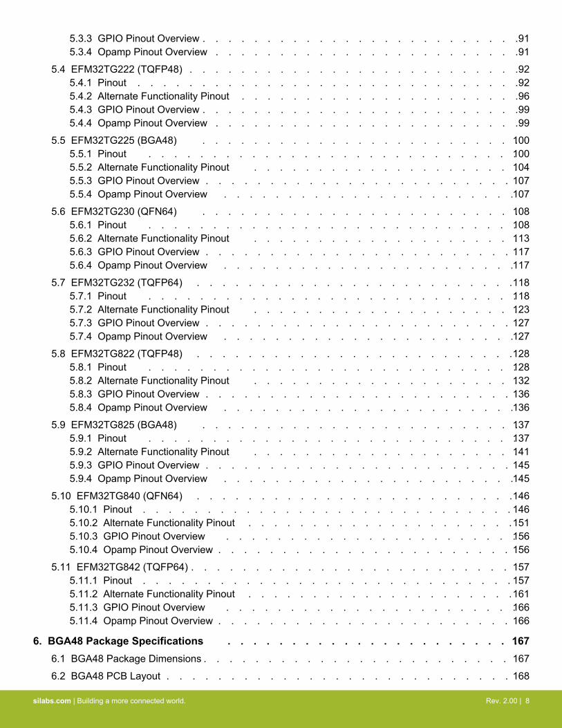
5.3.3 GPIO Pinout Overview . . . . . . . . . . . . . . . . . . . . . . . . .915.3.4 Opamp Pinout Overview . . . . . . . . . . . . . . . . . . . . . . . .91
5.4 EFM32TG222 (TQFP48) . . . . . . . . . . . . . . . . . . . . . . . . . .925.4.1 Pinout . . . . . . . . . . . . . . . . . . . . . . . . . . . . . .925.4.2 Alternate Functionality Pinout . . . . . . . . . . . . . . . . . . . . . .965.4.3 GPIO Pinout Overview . . . . . . . . . . . . . . . . . . . . . . . . .995.4.4 Opamp Pinout Overview . . . . . . . . . . . . . . . . . . . . . . . .99
5.5 EFM32TG225 (BGA48) . . . . . . . . . . . . . . . . . . . . . . . . .1005.5.1 Pinout . . . . . . . . . . . . . . . . . . . . . . . . . . . . .1005.5.2 Alternate Functionality Pinout . . . . . . . . . . . . . . . . . . . . .1045.5.3 GPIO Pinout Overview . . . . . . . . . . . . . . . . . . . . . . . . 1075.5.4 Opamp Pinout Overview . . . . . . . . . . . . . . . . . . . . . . .107
5.6 EFM32TG230 (QFN64) . . . . . . . . . . . . . . . . . . . . . . . . .1085.6.1 Pinout . . . . . . . . . . . . . . . . . . . . . . . . . . . . .1085.6.2 Alternate Functionality Pinout . . . . . . . . . . . . . . . . . . . . .1135.6.3 GPIO Pinout Overview . . . . . . . . . . . . . . . . . . . . . . . . 1175.6.4 Opamp Pinout Overview . . . . . . . . . . . . . . . . . . . . . . .117
5.7 EFM32TG232 (TQFP64) . . . . . . . . . . . . . . . . . . . . . . . . .1185.7.1 Pinout . . . . . . . . . . . . . . . . . . . . . . . . . . . . .1185.7.2 Alternate Functionality Pinout . . . . . . . . . . . . . . . . . . . . .1235.7.3 GPIO Pinout Overview . . . . . . . . . . . . . . . . . . . . . . . . 1275.7.4 Opamp Pinout Overview . . . . . . . . . . . . . . . . . . . . . . .127
5.8 EFM32TG822 (TQFP48) . . . . . . . . . . . . . . . . . . . . . . . . .1285.8.1 Pinout . . . . . . . . . . . . . . . . . . . . . . . . . . . . .1285.8.2 Alternate Functionality Pinout . . . . . . . . . . . . . . . . . . . . .1325.8.3 GPIO Pinout Overview . . . . . . . . . . . . . . . . . . . . . . . . 1365.8.4 Opamp Pinout Overview . . . . . . . . . . . . . . . . . . . . . . .136
5.9 EFM32TG825 (BGA48) . . . . . . . . . . . . . . . . . . . . . . . . .1375.9.1 Pinout . . . . . . . . . . . . . . . . . . . . . . . . . . . . .1375.9.2 Alternate Functionality Pinout . . . . . . . . . . . . . . . . . . . . .1415.9.3 GPIO Pinout Overview . . . . . . . . . . . . . . . . . . . . . . . . 1455.9.4 Opamp Pinout Overview . . . . . . . . . . . . . . . . . . . . . . .145
5.10 EFM32TG840 (QFN64) . . . . . . . . . . . . . . . . . . . . . . . . .1465.10.1 Pinout . . . . . . . . . . . . . . . . . . . . . . . . . . . . . 1465.10.2 Alternate Functionality Pinout . . . . . . . . . . . . . . . . . . . . .1515.10.3 GPIO Pinout Overview . . . . . . . . . . . . . . . . . . . . . . .1565.10.4 Opamp Pinout Overview . . . . . . . . . . . . . . . . . . . . . . . 156
5.11 EFM32TG842 (TQFP64) . . . . . . . . . . . . . . . . . . . . . . . . . 1575.11.1 Pinout . . . . . . . . . . . . . . . . . . . . . . . . . . . . . 1575.11.2 Alternate Functionality Pinout . . . . . . . . . . . . . . . . . . . . .1615.11.3 GPIO Pinout Overview . . . . . . . . . . . . . . . . . . . . . . .1665.11.4 Opamp Pinout Overview . . . . . . . . . . . . . . . . . . . . . . . 166
6. BGA48 Package Specifications . . . . . . . . . . . . . . . . . . . . . . .1676.1 BGA48 Package Dimensions . . . . . . . . . . . . . . . . . . . . . . . . 167
6.2 BGA48 PCB Layout . . . . . . . . . . . . . . . . . . . . . . . . . . . 168
silabs.com | Building a more connected world. Rev. 2.00 | 8
6.3 BGA48 Package Marking . . . . . . . . . . . . . . . . . . . . . . . . . 170
7. QFN24 Package Specifications. . . . . . . . . . . . . . . . . . . . . . . . 1717.1 QFN24 Package Dimensions . . . . . . . . . . . . . . . . . . . . . . . . 171
7.2 QFN24 PCB Layout . . . . . . . . . . . . . . . . . . . . . . . . . . . 172
7.3 QFN24 Package Marking . . . . . . . . . . . . . . . . . . . . . . . . . 174
8. QFN32 Package Specifications. . . . . . . . . . . . . . . . . . . . . . . . 1758.1 QFN32 Package Dimensions . . . . . . . . . . . . . . . . . . . . . . . . 175
8.2 QFN32 PCB Layout . . . . . . . . . . . . . . . . . . . . . . . . . . . 176
8.3 QFN32 Package Marking . . . . . . . . . . . . . . . . . . . . . . . . . 178
9. QFN64 Package Specifications. . . . . . . . . . . . . . . . . . . . . . . . 1799.1 QFN64 Package Dimensions . . . . . . . . . . . . . . . . . . . . . . . . 179
9.2 QFN64 PCB Layout . . . . . . . . . . . . . . . . . . . . . . . . . . . 181
9.3 QFN64 Package Marking . . . . . . . . . . . . . . . . . . . . . . . . . 183
10. TQFP48 Package Specifications . . . . . . . . . . . . . . . . . . . . . . . 18410.1 TQFP48 Package Dimensions . . . . . . . . . . . . . . . . . . . . . . . 184
10.2 TQFP48 PCB Layout . . . . . . . . . . . . . . . . . . . . . . . . . . 186
10.3 TQFP48 Package Marking . . . . . . . . . . . . . . . . . . . . . . . .188
11. TQFP64 Package Specifications . . . . . . . . . . . . . . . . . . . . . . . 18911.1 TQFP64 Package Dimensions . . . . . . . . . . . . . . . . . . . . . . . 189
11.2 TQFP64 PCB Layout . . . . . . . . . . . . . . . . . . . . . . . . . . 191
11.3 TQFP64 Package Marking . . . . . . . . . . . . . . . . . . . . . . . .193
12. Chip Revision, Solder Information, Errata . . . . . . . . . . . . . . . . . . .19412.1 Chip Revision . . . . . . . . . . . . . . . . . . . . . . . . . . . .194
12.2 Soldering Information . . . . . . . . . . . . . . . . . . . . . . . . . . 194
12.3 Errata . . . . . . . . . . . . . . . . . . . . . . . . . . . . . . .194
13. Revision History. . . . . . . . . . . . . . . . . . . . . . . . . . . . . 19513.1 Revision 2.00 . . . . . . . . . . . . . . . . . . . . . . . . . . . .195
13.2 Revision 1.40 . . . . . . . . . . . . . . . . . . . . . . . . . . . .196
13.3 Revision 1.30 . . . . . . . . . . . . . . . . . . . . . . . . . . . .197
13.4 Revision 1.21 . . . . . . . . . . . . . . . . . . . . . . . . . . . .197
13.5 Revision 1.20 . . . . . . . . . . . . . . . . . . . . . . . . . . . .198
13.6 Revision 1.10 . . . . . . . . . . . . . . . . . . . . . . . . . . . .198
13.7 Revision 1.00 . . . . . . . . . . . . . . . . . . . . . . . . . . . .199
13.8 Revision 0.96 . . . . . . . . . . . . . . . . . . . . . . . . . . . .199
13.9 Revision 0.95 . . . . . . . . . . . . . . . . . . . . . . . . . . . .200
13.10 Revision 0.92 . . . . . . . . . . . . . . . . . . . . . . . . . . . .200
silabs.com | Building a more connected world. Rev. 2.00 | 9

13.11 Revision 0.91 . . . . . . . . . . . . . . . . . . . . . . . . . . . .201
13.12 Revision 0.90 . . . . . . . . . . . . . . . . . . . . . . . . . . . .201
13.13 Revision 0.70 . . . . . . . . . . . . . . . . . . . . . . . . . . . .202
13.14 Revision 0.60 . . . . . . . . . . . . . . . . . . . . . . . . . . . .202
13.15 Revision 0.50 . . . . . . . . . . . . . . . . . . . . . . . . . . . .202
13.16 Revision 0.40 . . . . . . . . . . . . . . . . . . . . . . . . . . . .202
silabs.com | Building a more connected world. Rev. 2.00 | 10
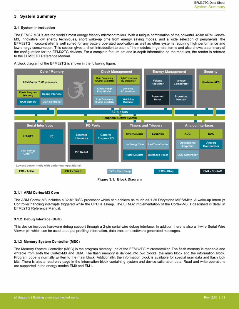
3. System Summary
3.1 System Introduction
The EFM32 MCUs are the world’s most energy friendly microcontrollers. With a unique combination of the powerful 32-bit ARM Cortex-M3, innovative low energy techniques, short wake-up time from energy saving modes, and a wide selection of peripherals, theEFM32TG microcontroller is well suited for any battery operated application as well as other systems requiring high performance andlow-energy consumption. This section gives a short introduction to each of the modules in general terms and also shows a summary ofthe configuration for the EFM32TG devices. For a complete feature set and in-depth information on the modules, the reader is referredto the EFM32TG Reference Manual.
A block diagram of the EFM32TG is shown in the following figure.
32-bit bus
Lowest power mode with peripheral operational:
EM2 – Deep SleepEM1 - Sleep EM4 - ShutoffEM0 - Active EM3 - Stop
Core / Memory
Flash Program Memory
RAM Memory
ARM CortexTM M3 processor
Debug Interface
DMA Controller
Security
Hardware AES
Energy Management
Power-on Reset
Voltage Regulator
Voltage Comparator
Brown-out Detector
Clock Management
High Frequency RC Oscillator
Low Freq. RC Oscillator
Low FrequencyCrystal Oscillator
Watchdog Oscillator
Auxiliary High Freq. RC Osc.
High Frequency Crystal Oscillator
Analog Interfaces
DACADC
Operational Amplifier
Analog Comparator
Peripheral Reflex System
Serial Interfaces
I2C
I/O Ports Timers and Triggers
Timer/Counter
Low Energy Timer Real Time Counter
External Interrupts
General Purpose I/O
LESENSE
Pulse Counter
USART
Low Energy UARTTM Pin Reset
Watchdog Timer LCD Controller
Figure 3.1. Block Diagram
3.1.1 ARM Cortex-M3 Core
The ARM Cortex-M3 includes a 32-bit RISC processor which can achieve as much as 1.25 Dhrystone MIPS/MHz. A wake-up InterruptController handling interrupts triggered while the CPU is asleep. The EFM32 implementation of the Cortex-M3 is described in detail inEFM32TG Reference Manual.
3.1.2 Debug Interface (DBG)
This device includes hardware debug support through a 2-pin serial-wire debug interface. In addition there is also a 1-wire Serial WireViewer pin which can be used to output profiling information, data trace and software-generated messages.
3.1.3 Memory System Controller (MSC)
The Memory System Controller (MSC) is the program memory unit of the EFM32TG microcontroller. The flash memory is readable andwritable from both the Cortex-M3 and DMA. The flash memory is divided into two blocks; the main block and the information block.Program code is normally written to the main block. Additionally, the information block is available for special user data and flash lockbits. There is also a read-only page in the information block containing system and device calibration data. Read and write operationsare supported in the energy modes EM0 and EM1.
EFM32TG Data SheetSystem Summary
silabs.com | Building a more connected world. Rev. 2.00 | 11
3.1.4 Direct Memory Access Controller (DMA)
The Direct Memory Access (DMA) controller performs memory operations independently of the CPU. This has the benefit of reducingthe energy consumption and the workload of the CPU, and enables the system to stay in low energy modes when moving for instancedata from the USART to RAM or from the External Bus Interface to a PWM-generating timer. The DMA controller uses the PL230µDMA controller licensed from ARM.
3.1.5 Reset Management Unit (RMU)
The RMU is responsible for handling the reset functionality of the EFM32TG.
3.1.6 Energy Management Unit (EMU)
The Energy Management Unit (EMU) manage all the low energy modes (EM) in EFM32TG microcontrollers. Each energy mode man-ages if the CPU and the various peripherals are available. The EMU can also be used to turn off the power to unused SRAM blocks.
3.1.7 Clock Management Unit (CMU)
The Clock Management Unit (CMU) is responsible for controlling the oscillators and clocks on-board the EFM32TG. The CMU providesthe capability to turn on and off the clock on an individual basis to all peripheral modules in addition to enable/disable and configure theavailable oscillators. The high degree of flexibility enables software to minimize energy consumption in any specific application by notwasting power on peripherals and oscillators that are inactive.
3.1.8 Watchdog (WDOG)
The purpose of the watchdog timer is to generate a reset in case of a system failure, to increase application reliability. The failure maye.g. be caused by an external event, such as an ESD pulse, or by a software failure.
3.1.9 Peripheral Reflex System (PRS)
The Peripheral Reflex System (PRS) system is a network which lets the different peripheral module communicate directly with eachother without involving the CPU. Peripheral modules which send out Reflex signals are called producers. The PRS routes these reflexsignals to consumer peripherals which apply actions depending on the data received. The format for the Reflex signals is not given, butedge triggers and other functionality can be applied by the PRS.
3.1.10 Inter-Integrated Circuit Interface (I2C)
The I2C module provides an interface between the MCU and a serial I2C-bus. It is capable of acting as both a master and a slave, andsupports multi-master buses. Both standard-mode, fast-mode and fastmode plus speeds are supported, allowing transmission rates allthe way from 10 kbit/s up to 1 Mbit/s. Slave arbitration and timeouts are also provided to allow implementation of an SMBus compliantsystem. The interface provided to software by the I2C module, allows both fine-grained control of the transmission process and close toautomatic transfers. Automatic recognition of slave addresses is provided in all energy modes.
3.1.11 Universal Synchronous/Asynchronous Receiver/Transmitter (USART)
The Universal Synchronous Asynchronous serial Receiver and Transmitter (USART) is a very flexible serial I/O module. It supports fullduplex asynchronous UART communication as well as RS-485, SPI, MicroWire and 3-wire. It can also interface with ISO7816 Smart-Cards, IrDA and I2S devices.
3.1.12 Pre-Programmed UART Bootloader
The bootloader presented in application note AN0003 is pre-programmed in the device at factory. Autobaud and destructive write aresupported. The autobaud feature, interface and commands are described further in the application note.
3.1.13 Low Energy Universal Asynchronous Receiver/Transmitter (LEUART)
The unique LEUARTTM, the Low Energy UART, is a UART that allows two-way UART communication on a strict power budget. Only a32.768 kHz clock is needed to allow UART communication up to 9600 baud/ s. The LEUART includes all necessary hardware supportto make asynchronous serial communication possible with minimum of software intervention and energy consumption.
EFM32TG Data SheetSystem Summary
silabs.com | Building a more connected world. Rev. 2.00 | 12
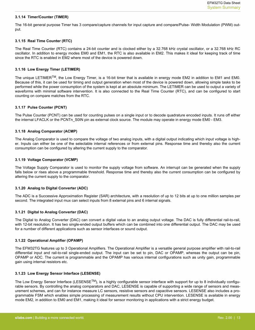
3.1.14 Timer/Counter (TIMER)
The 16-bit general purpose Timer has 3 compare/capture channels for input capture and compare/Pulse- Width Modulation (PWM) out-put.
3.1.15 Real Time Counter (RTC)
The Real Time Counter (RTC) contains a 24-bit counter and is clocked either by a 32.768 kHz crystal oscillator, or a 32.768 kHz RCoscillator. In addition to energy modes EM0 and EM1, the RTC is also available in EM2. This makes it ideal for keeping track of timesince the RTC is enabled in EM2 where most of the device is powered down.
3.1.16 Low Energy Timer (LETIMER)
The unique LETIMERTM, the Low Energy Timer, is a 16-bit timer that is available in energy mode EM2 in addition to EM1 and EM0.Because of this, it can be used for timing and output generation when most of the device is powered down, allowing simple tasks to beperformed while the power consumption of the system is kept at an absolute minimum. The LETIMER can be used to output a variety ofwaveforms with minimal software intervention. It is also connected to the Real Time Counter (RTC), and can be configured to startcounting on compare matches from the RTC.
3.1.17 Pulse Counter (PCNT)
The Pulse Counter (PCNT) can be used for counting pulses on a single input or to decode quadrature encoded inputs. It runs off eitherthe internal LFACLK or the PCNTn_S0IN pin as external clock source. The module may operate in energy mode EM0 - EM3.
3.1.18 Analog Comparator (ACMP)
The Analog Comparator is used to compare the voltage of two analog inputs, with a digital output indicating which input voltage is high-er. Inputs can either be one of the selectable internal references or from external pins. Response time and thereby also the currentconsumption can be configured by altering the current supply to the comparator.
3.1.19 Voltage Comparator (VCMP)
The Voltage Supply Comparator is used to monitor the supply voltage from software. An interrupt can be generated when the supplyfalls below or rises above a programmable threshold. Response time and thereby also the current consumption can be configured byaltering the current supply to the comparator.
3.1.20 Analog to Digital Converter (ADC)
The ADC is a Successive Approximation Register (SAR) architecture, with a resolution of up to 12 bits at up to one million samples persecond. The integrated input mux can select inputs from 8 external pins and 6 internal signals.
3.1.21 Digital to Analog Converter (DAC)
The Digital to Analog Converter (DAC) can convert a digital value to an analog output voltage. The DAC is fully differential rail-to-rail,with 12-bit resolution. It has two single-ended output buffers which can be combined into one differential output. The DAC may be usedfor a number of different applications such as sensor interfaces or sound output.
3.1.22 Operational Amplifier (OPAMP)
The EFM32TG features up to 3 Operational Amplifiers. The Operational Amplifier is a versatile general purpose amplifier with rail-to-raildifferential input and rail-to-rail single-ended output. The input can be set to pin, DAC or OPAMP, whereas the output can be pin,OPAMP or ADC. The current is programmable and the OPAMP has various internal configurations such as unity gain, programmablegain using internal resistors etc.
3.1.23 Low Energy Sensor Interface (LESENSE)
The Low Energy Sensor Interface (LESENSETM), is a highly configurable sensor interface with support for up to 8 individually configu-rable sensors. By controlling the analog comparators and DAC, LESENSE is capable of supporting a wide range of sensors and meas-urement schemes, and can for instance measure LC sensors, resistive sensors and capacitive sensors. LESENSE also includes a pro-grammable FSM which enables simple processing of measurement results without CPU intervention. LESENSE is available in energymode EM2, in addition to EM0 and EM1, making it ideal for sensor monitoring in applications with a strict energy budget.
EFM32TG Data SheetSystem Summary
silabs.com | Building a more connected world. Rev. 2.00 | 13
3.1.24 Advanced Encryption Standard Accelerator (AES)
The AES accelerator performs AES encryption and decryption with 128-bit or 256-bit keys. Encrypting or decrypting one 128-bit datablock takes 52 HFCORECLK cycles with 128-bit keys and 75 HFCORECLK cycles with 256-bit keys. The AES module is an AHB slavewhich enables efficient access to the data and key registers. All write accesses to the AES module must be 32-bit operations, i.e. 8- or16-bit operations are not supported.
3.1.25 General Purpose Input/Output (GPIO)
In the EFM32TG, there are up to 56 General Purpose Input/Output (GPIO) pins, which are divided into ports with up to 16 pins each.These pins can individually be configured as either an output or input. More advanced configurations like open-drain, filtering and drivestrength can also be configured individually for the pins. The GPIO pins can also be overridden by peripheral pin connections, like Tim-er PWM outputs or USART communication, which can be routed to several locations on the device. The GPIO supports up to 16 asyn-chronous external pin interrupts, which enables interrupts from any pin on the device. Also, the input value of a pin can be routedthrough the Peripheral Reflex System to other peripherals.
3.1.26 Liquid Crystal Display Driver (LCD)
The LCD driver is capable of driving a segmented LCD display with up to 8x20 segments. A voltage boost function enables it to providethe LCD display with higher voltage than the supply voltage for the device. In addition, an animation feature can run custom animationson the LCD display without any CPU intervention. The LCD driver can also remain active even in Energy Mode 2 and provides a FrameCounter interrupt that can wake-up the device on a regular basis for updating data.
EFM32TG Data SheetSystem Summary
silabs.com | Building a more connected world. Rev. 2.00 | 14
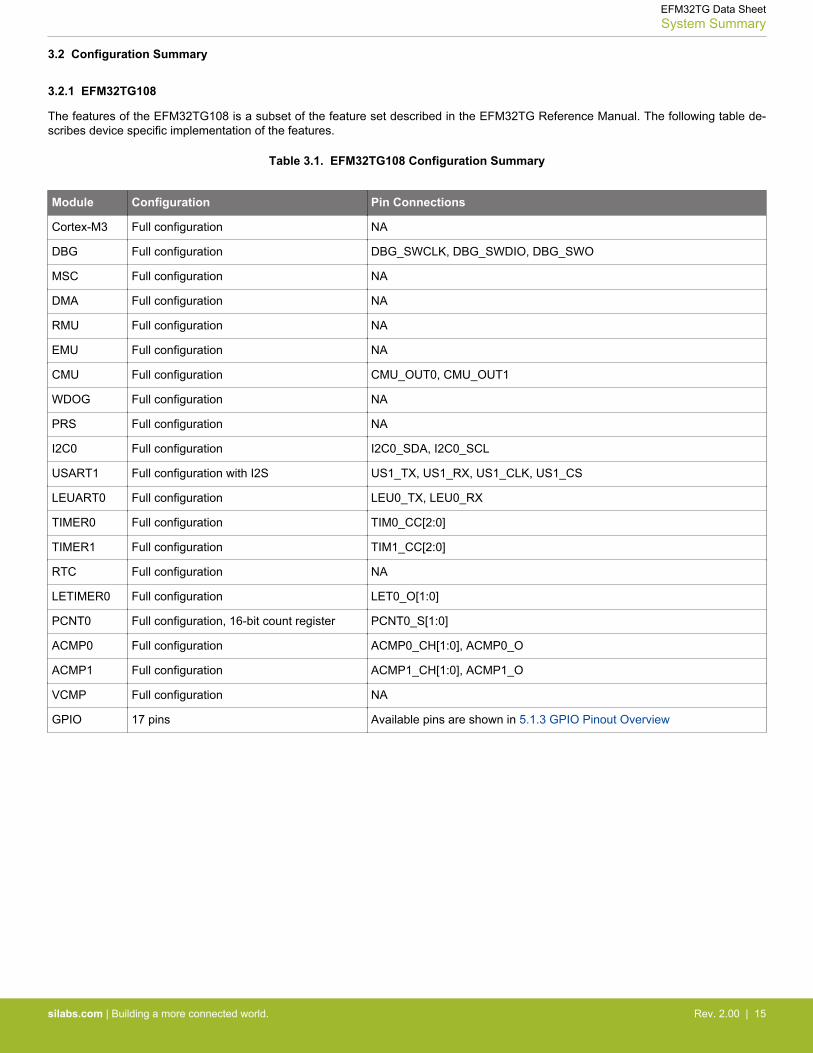
3.2 Configuration Summary
3.2.1 EFM32TG108
The features of the EFM32TG108 is a subset of the feature set described in the EFM32TG Reference Manual. The following table de-scribes device specific implementation of the features.
Table 3.1. EFM32TG108 Configuration Summary
Module Configuration Pin Connections
Cortex-M3 Full configuration NA
DBG Full configuration DBG_SWCLK, DBG_SWDIO, DBG_SWO
MSC Full configuration NA
DMA Full configuration NA
RMU Full configuration NA
EMU Full configuration NA
CMU Full configuration CMU_OUT0, CMU_OUT1
WDOG Full configuration NA
PRS Full configuration NA
I2C0 Full configuration I2C0_SDA, I2C0_SCL
USART1 Full configuration with I2S US1_TX, US1_RX, US1_CLK, US1_CS
LEUART0 Full configuration LEU0_TX, LEU0_RX
TIMER0 Full configuration TIM0_CC[2:0]
TIMER1 Full configuration TIM1_CC[2:0]
RTC Full configuration NA
LETIMER0 Full configuration LET0_O[1:0]
PCNT0 Full configuration, 16-bit count register PCNT0_S[1:0]
ACMP0 Full configuration ACMP0_CH[1:0], ACMP0_O
ACMP1 Full configuration ACMP1_CH[1:0], ACMP1_O
VCMP Full configuration NA
GPIO 17 pins Available pins are shown in 5.1.3 GPIO Pinout Overview
EFM32TG Data SheetSystem Summary
silabs.com | Building a more connected world. Rev. 2.00 | 15
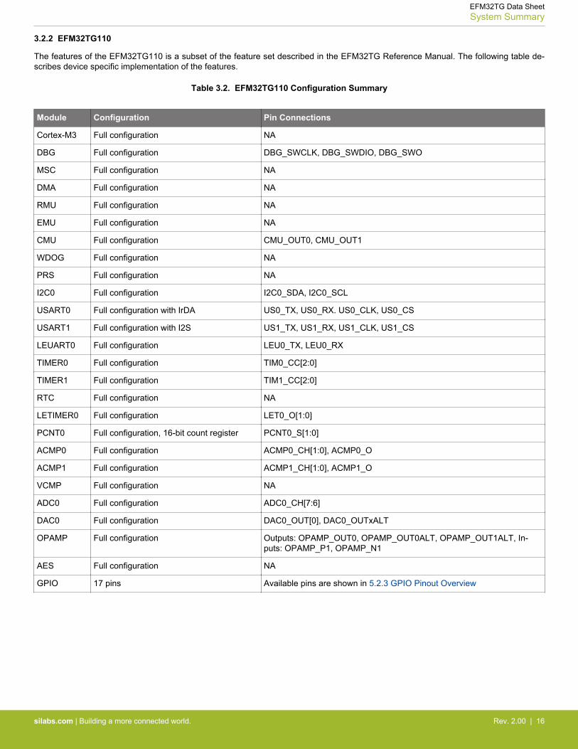
3.2.2 EFM32TG110
The features of the EFM32TG110 is a subset of the feature set described in the EFM32TG Reference Manual. The following table de-scribes device specific implementation of the features.
Table 3.2. EFM32TG110 Configuration Summary
Module Configuration Pin Connections
Cortex-M3 Full configuration NA
DBG Full configuration DBG_SWCLK, DBG_SWDIO, DBG_SWO
MSC Full configuration NA
DMA Full configuration NA
RMU Full configuration NA
EMU Full configuration NA
CMU Full configuration CMU_OUT0, CMU_OUT1
WDOG Full configuration NA
PRS Full configuration NA
I2C0 Full configuration I2C0_SDA, I2C0_SCL
USART0 Full configuration with IrDA US0_TX, US0_RX. US0_CLK, US0_CS
USART1 Full configuration with I2S US1_TX, US1_RX, US1_CLK, US1_CS
LEUART0 Full configuration LEU0_TX, LEU0_RX
TIMER0 Full configuration TIM0_CC[2:0]
TIMER1 Full configuration TIM1_CC[2:0]
RTC Full configuration NA
LETIMER0 Full configuration LET0_O[1:0]
PCNT0 Full configuration, 16-bit count register PCNT0_S[1:0]
ACMP0 Full configuration ACMP0_CH[1:0], ACMP0_O
ACMP1 Full configuration ACMP1_CH[1:0], ACMP1_O
VCMP Full configuration NA
ADC0 Full configuration ADC0_CH[7:6]
DAC0 Full configuration DAC0_OUT[0], DAC0_OUTxALT
OPAMP Full configuration Outputs: OPAMP_OUT0, OPAMP_OUT0ALT, OPAMP_OUT1ALT, In-puts: OPAMP_P1, OPAMP_N1
AES Full configuration NA
GPIO 17 pins Available pins are shown in 5.2.3 GPIO Pinout Overview
EFM32TG Data SheetSystem Summary
silabs.com | Building a more connected world. Rev. 2.00 | 16
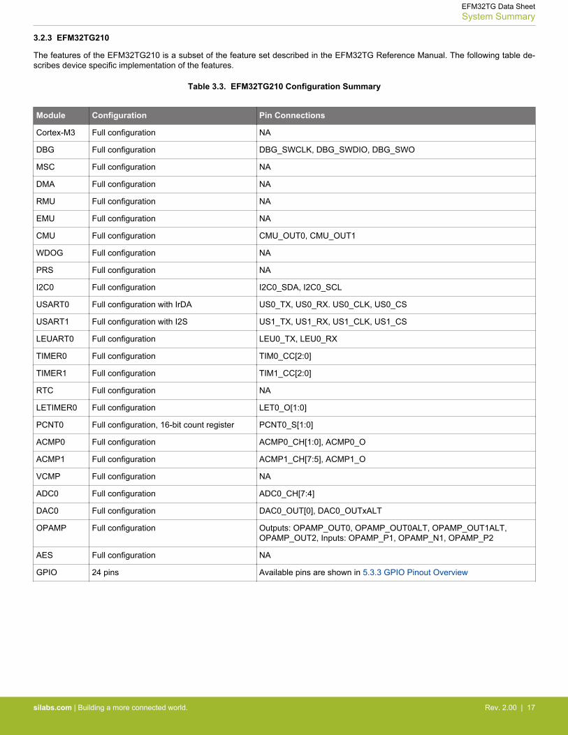
3.2.3 EFM32TG210
The features of the EFM32TG210 is a subset of the feature set described in the EFM32TG Reference Manual. The following table de-scribes device specific implementation of the features.
Table 3.3. EFM32TG210 Configuration Summary
Module Configuration Pin Connections
Cortex-M3 Full configuration NA
DBG Full configuration DBG_SWCLK, DBG_SWDIO, DBG_SWO
MSC Full configuration NA
DMA Full configuration NA
RMU Full configuration NA
EMU Full configuration NA
CMU Full configuration CMU_OUT0, CMU_OUT1
WDOG Full configuration NA
PRS Full configuration NA
I2C0 Full configuration I2C0_SDA, I2C0_SCL
USART0 Full configuration with IrDA US0_TX, US0_RX. US0_CLK, US0_CS
USART1 Full configuration with I2S US1_TX, US1_RX, US1_CLK, US1_CS
LEUART0 Full configuration LEU0_TX, LEU0_RX
TIMER0 Full configuration TIM0_CC[2:0]
TIMER1 Full configuration TIM1_CC[2:0]
RTC Full configuration NA
LETIMER0 Full configuration LET0_O[1:0]
PCNT0 Full configuration, 16-bit count register PCNT0_S[1:0]
ACMP0 Full configuration ACMP0_CH[1:0], ACMP0_O
ACMP1 Full configuration ACMP1_CH[7:5], ACMP1_O
VCMP Full configuration NA
ADC0 Full configuration ADC0_CH[7:4]
DAC0 Full configuration DAC0_OUT[0], DAC0_OUTxALT
OPAMP Full configuration Outputs: OPAMP_OUT0, OPAMP_OUT0ALT, OPAMP_OUT1ALT,OPAMP_OUT2, Inputs: OPAMP_P1, OPAMP_N1, OPAMP_P2
AES Full configuration NA
GPIO 24 pins Available pins are shown in 5.3.3 GPIO Pinout Overview
EFM32TG Data SheetSystem Summary
silabs.com | Building a more connected world. Rev. 2.00 | 17

3.2.4 EFM32TG222
The features of the EFM32TG222 is a subset of the feature set described in the EFM32TG Reference Manual. The following table de-scribes device specific implementation of the features.
Table 3.4. EFM32TG222 Configuration Summary
Module Configuration Pin Connections
Cortex-M3 Full configuration NA
DBG Full configuration DBG_SWCLK, DBG_SWDIO, DBG_SWO
MSC Full configuration NA
DMA Full configuration NA
RMU Full configuration NA
EMU Full configuration NA
CMU Full configuration CMU_OUT0, CMU_OUT1
WDOG Full configuration NA
PRS Full configuration NA
I2C0 Full configuration I2C0_SDA, I2C0_SCL
USART0 Full configuration with IrDA US0_TX, US0_RX. US0_CLK, US0_CS
USART1 Full configuration with I2S US1_TX, US1_RX, US1_CLK, US1_CS
LEUART0 Full configuration LEU0_TX, LEU0_RX
TIMER0 Full configuration TIM0_CC[2:0]
TIMER1 Full configuration TIM1_CC[2:0]
RTC Full configuration NA
LETIMER0 Full configuration LET0_O[1:0]
PCNT0 Full configuration, 16-bit count register PCNT0_S[1:0]
ACMP0 Full configuration ACMP0_CH[4:0], ACMP0_O
ACMP1 Full configuration ACMP1_CH[7:0], ACMP1_O
VCMP Full configuration NA
ADC0 Full configuration ADC0_CH[7:4]
DAC0 Full configuration DAC0_OUT[1], DAC0_OUTxALT
OPAMP Full configuration Outputs: OPAMP_OUT0, OPAMP_OUT0ALT, OPAMP_OUT1ALT,OPAMP_OUT2, Inputs: OPAMP_P0, OPAMP_P1, OPAMP_N1,OPAMP_P2
AES Full configuration NA
GPIO 37 pins Available pins are shown in 5.4.3 GPIO Pinout Overview
EFM32TG Data SheetSystem Summary
silabs.com | Building a more connected world. Rev. 2.00 | 18
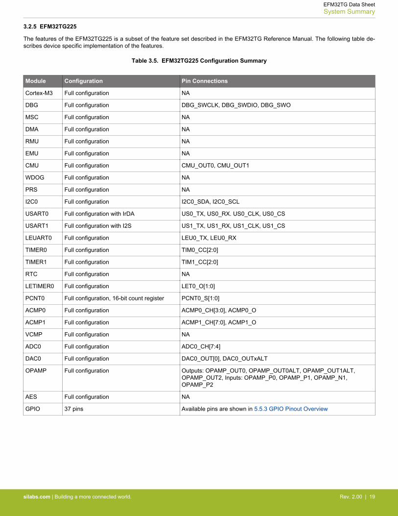
3.2.5 EFM32TG225
The features of the EFM32TG225 is a subset of the feature set described in the EFM32TG Reference Manual. The following table de-scribes device specific implementation of the features.
Table 3.5. EFM32TG225 Configuration Summary
Module Configuration Pin Connections
Cortex-M3 Full configuration NA
DBG Full configuration DBG_SWCLK, DBG_SWDIO, DBG_SWO
MSC Full configuration NA
DMA Full configuration NA
RMU Full configuration NA
EMU Full configuration NA
CMU Full configuration CMU_OUT0, CMU_OUT1
WDOG Full configuration NA
PRS Full configuration NA
I2C0 Full configuration I2C0_SDA, I2C0_SCL
USART0 Full configuration with IrDA US0_TX, US0_RX. US0_CLK, US0_CS
USART1 Full configuration with I2S US1_TX, US1_RX, US1_CLK, US1_CS
LEUART0 Full configuration LEU0_TX, LEU0_RX
TIMER0 Full configuration TIM0_CC[2:0]
TIMER1 Full configuration TIM1_CC[2:0]
RTC Full configuration NA
LETIMER0 Full configuration LET0_O[1:0]
PCNT0 Full configuration, 16-bit count register PCNT0_S[1:0]
ACMP0 Full configuration ACMP0_CH[3:0], ACMP0_O
ACMP1 Full configuration ACMP1_CH[7:0], ACMP1_O
VCMP Full configuration NA
ADC0 Full configuration ADC0_CH[7:4]
DAC0 Full configuration DAC0_OUT[0], DAC0_OUTxALT
OPAMP Full configuration Outputs: OPAMP_OUT0, OPAMP_OUT0ALT, OPAMP_OUT1ALT,OPAMP_OUT2, Inputs: OPAMP_P0, OPAMP_P1, OPAMP_N1,OPAMP_P2
AES Full configuration NA
GPIO 37 pins Available pins are shown in 5.5.3 GPIO Pinout Overview
EFM32TG Data SheetSystem Summary
silabs.com | Building a more connected world. Rev. 2.00 | 19
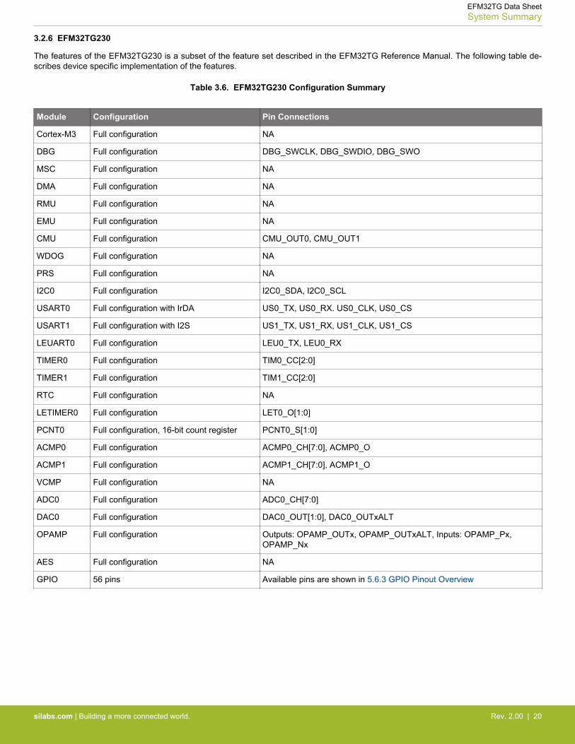
3.2.6 EFM32TG230
The features of the EFM32TG230 is a subset of the feature set described in the EFM32TG Reference Manual. The following table de-scribes device specific implementation of the features.
Table 3.6. EFM32TG230 Configuration Summary
Module Configuration Pin Connections
Cortex-M3 Full configuration NA
DBG Full configuration DBG_SWCLK, DBG_SWDIO, DBG_SWO
MSC Full configuration NA
DMA Full configuration NA
RMU Full configuration NA
EMU Full configuration NA
CMU Full configuration CMU_OUT0, CMU_OUT1
WDOG Full configuration NA
PRS Full configuration NA
I2C0 Full configuration I2C0_SDA, I2C0_SCL
USART0 Full configuration with IrDA US0_TX, US0_RX. US0_CLK, US0_CS
USART1 Full configuration with I2S US1_TX, US1_RX, US1_CLK, US1_CS
LEUART0 Full configuration LEU0_TX, LEU0_RX
TIMER0 Full configuration TIM0_CC[2:0]
TIMER1 Full configuration TIM1_CC[2:0]
RTC Full configuration NA
LETIMER0 Full configuration LET0_O[1:0]
PCNT0 Full configuration, 16-bit count register PCNT0_S[1:0]
ACMP0 Full configuration ACMP0_CH[7:0], ACMP0_O
ACMP1 Full configuration ACMP1_CH[7:0], ACMP1_O
VCMP Full configuration NA
ADC0 Full configuration ADC0_CH[7:0]
DAC0 Full configuration DAC0_OUT[1:0], DAC0_OUTxALT
OPAMP Full configuration Outputs: OPAMP_OUTx, OPAMP_OUTxALT, Inputs: OPAMP_Px,OPAMP_Nx
AES Full configuration NA
GPIO 56 pins Available pins are shown in 5.6.3 GPIO Pinout Overview
EFM32TG Data SheetSystem Summary
silabs.com | Building a more connected world. Rev. 2.00 | 20
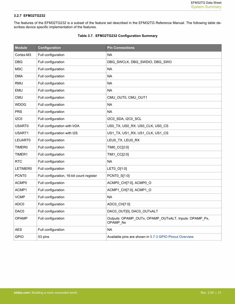
3.2.7 EFM32TG232
The features of the EFM32TG232 is a subset of the feature set described in the EFM32TG Reference Manual. The following table de-scribes device specific implementation of the features.
Table 3.7. EFM32TG232 Configuration Summary
Module Configuration Pin Connections
Cortex-M3 Full configuration NA
DBG Full configuration DBG_SWCLK, DBG_SWDIO, DBG_SWO
MSC Full configuration NA
DMA Full configuration NA
RMU Full configuration NA
EMU Full configuration NA
CMU Full configuration CMU_OUT0, CMU_OUT1
WDOG Full configuration NA
PRS Full configuration NA
I2C0 Full configuration I2C0_SDA, I2C0_SCL
USART0 Full configuration with IrDA US0_TX, US0_RX. US0_CLK, US0_CS
USART1 Full configuration with I2S US1_TX, US1_RX, US1_CLK, US1_CS
LEUART0 Full configuration LEU0_TX, LEU0_RX
TIMER0 Full configuration TIM0_CC[2:0]
TIMER1 Full configuration TIM1_CC[2:0]
RTC Full configuration NA
LETIMER0 Full configuration LET0_O[1:0]
PCNT0 Full configuration, 16-bit count register PCNT0_S[1:0]
ACMP0 Full configuration ACMP0_CH[7:0], ACMP0_O
ACMP1 Full configuration ACMP1_CH[7:0], ACMP1_O
VCMP Full configuration NA
ADC0 Full configuration ADC0_CH[7:0]
DAC0 Full configuration DAC0_OUT[0], DAC0_OUTxALT
OPAMP Full configuration Outputs: OPAMP_OUTx, OPAMP_OUTxALT, Inputs: OPAMP_Px,OPAMP_Nx
AES Full configuration NA
GPIO 53 pins Available pins are shown in 5.7.3 GPIO Pinout Overview
EFM32TG Data SheetSystem Summary
silabs.com | Building a more connected world. Rev. 2.00 | 21

3.2.8 EFM32TG822
The features of the EFM32TG822 is a subset of the feature set described in the EFM32TG Reference Manual. The following table de-scribes device specific implementation of the features.
Table 3.8. EFM32TG822 Configuration Summary
Module Configuration Pin Connections
Cortex-M3 Full configuration NA
DBG Full configuration DBG_SWCLK, DBG_SWDIO, DBG_SWO
MSC Full configuration NA
DMA Full configuration NA
RMU Full configuration NA
EMU Full configuration NA
CMU Full configuration CMU_OUT0, CMU_OUT1
WDOG Full configuration NA
PRS Full configuration NA
I2C0 Full configuration I2C0_SDA, I2C0_SCL
USART0 Full configuration with IrDA US0_TX, US0_RX. US0_CLK, US0_CS
USART1 Full configuration with I2S US1_TX, US1_RX, US1_CLK, US1_CS
LEUART0 Full configuration LEU0_TX, LEU0_RX
TIMER0 Full configuration TIM0_CC[2:0]
TIMER1 Full configuration TIM1_CC[2:0]
RTC Full configuration NA
LETIMER0 Full configuration LET0_O[1:0]
PCNT0 Full configuration, 16-bit count register PCNT0_S[1:0]
ACMP0 Full configuration ACMP0_CH[4], ACMP0_O
ACMP1 Full configuration ACMP1_CH[7:5], ACMP1_O
VCMP Full configuration NA
ADC0 Full configuration ADC0_CH[7:4]
DAC0 Full configuration DAC0_OUT[0], DAC0_OUTxALT
OPAMP Full configuration Outputs: OPAMP_OUT0, OPAMP_OUT1ALT, OPAMP_OUT2, Inputs:OPAMP_P0, OPAMP_P1, OPAMP_N1, OPAMP_P2
AES Full configuration NA
GPIO 37 pins Available pins are shown in 5.8.3 GPIO Pinout Overview
LCD Full configuration LCD_SEG[10:0], LCD_COM[7:0], LCD_BCAP_P, LCD_BCAP_N,LCD_BEXT
EFM32TG Data SheetSystem Summary
silabs.com | Building a more connected world. Rev. 2.00 | 22
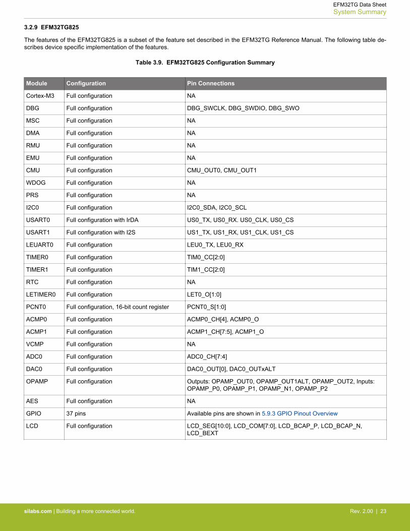
3.2.9 EFM32TG825
The features of the EFM32TG825 is a subset of the feature set described in the EFM32TG Reference Manual. The following table de-scribes device specific implementation of the features.
Table 3.9. EFM32TG825 Configuration Summary
Module Configuration Pin Connections
Cortex-M3 Full configuration NA
DBG Full configuration DBG_SWCLK, DBG_SWDIO, DBG_SWO
MSC Full configuration NA
DMA Full configuration NA
RMU Full configuration NA
EMU Full configuration NA
CMU Full configuration CMU_OUT0, CMU_OUT1
WDOG Full configuration NA
PRS Full configuration NA
I2C0 Full configuration I2C0_SDA, I2C0_SCL
USART0 Full configuration with IrDA US0_TX, US0_RX. US0_CLK, US0_CS
USART1 Full configuration with I2S US1_TX, US1_RX, US1_CLK, US1_CS
LEUART0 Full configuration LEU0_TX, LEU0_RX
TIMER0 Full configuration TIM0_CC[2:0]
TIMER1 Full configuration TIM1_CC[2:0]
RTC Full configuration NA
LETIMER0 Full configuration LET0_O[1:0]
PCNT0 Full configuration, 16-bit count register PCNT0_S[1:0]
ACMP0 Full configuration ACMP0_CH[4], ACMP0_O
ACMP1 Full configuration ACMP1_CH[7:5], ACMP1_O
VCMP Full configuration NA
ADC0 Full configuration ADC0_CH[7:4]
DAC0 Full configuration DAC0_OUT[0], DAC0_OUTxALT
OPAMP Full configuration Outputs: OPAMP_OUT0, OPAMP_OUT1ALT, OPAMP_OUT2, Inputs:OPAMP_P0, OPAMP_P1, OPAMP_N1, OPAMP_P2
AES Full configuration NA
GPIO 37 pins Available pins are shown in 5.9.3 GPIO Pinout Overview
LCD Full configuration LCD_SEG[10:0], LCD_COM[7:0], LCD_BCAP_P, LCD_BCAP_N,LCD_BEXT
EFM32TG Data SheetSystem Summary
silabs.com | Building a more connected world. Rev. 2.00 | 23

3.2.10 EFM32TG840
The features of the EFM32TG840 is a subset of the feature set described in the EFM32TG Reference Manual. The following table de-scribes device specific implementation of the features.
Table 3.10. EFM32TG840 Configuration Summary
Module Configuration Pin Connections
Cortex-M3 Full configuration NA
DBG Full configuration DBG_SWCLK, DBG_SWDIO, DBG_SWO
MSC Full configuration NA
DMA Full configuration NA
RMU Full configuration NA
EMU Full configuration NA
CMU Full configuration CMU_OUT0, CMU_OUT1
WDOG Full configuration NA
PRS Full configuration NA
I2C0 Full configuration I2C0_SDA, I2C0_SCL
USART0 Full configuration with IrDA US0_TX, US0_RX. US0_CLK, US0_CS
USART1 Full configuration with I2S US1_TX, US1_RX, US1_CLK, US1_CS
LEUART0 Full configuration LEU0_TX, LEU0_RX
TIMER0 Full configuration TIM0_CC[2:0]
TIMER1 Full configuration TIM1_CC[2:0]
RTC Full configuration NA
LETIMER0 Full configuration LET0_O[1:0]
PCNT0 Full configuration, 16-bit count register PCNT0_S[1:0]
ACMP0 Full configuration ACMP0_CH[7:4], ACMP0_O
ACMP1 Full configuration ACMP1_CH[7:4], ACMP1_O
VCMP Full configuration NA
ADC0 Full configuration ADC0_CH[7:0]
DAC0 Full configuration DAC0_OUT[0], DAC0_OUTxALT
OPAMP Full configuration Outputs: OPAMP_OUT0, OPAMP_OUT0ALT, OPAMP_OUT1ALT,OPAMP_OUT2, Inputs: OPAMP_Px, OPAMP_Nx
AES Full configuration NA
GPIO 56 pins Available pins are shown in 5.10.3 GPIO Pinout Overview
LCD Full configuration LCD_SEG[19:0], LCD_COM[7:0], LCD_BCAP_P, LCD_BCAP_N,LCD_BEXT
EFM32TG Data SheetSystem Summary
silabs.com | Building a more connected world. Rev. 2.00 | 24
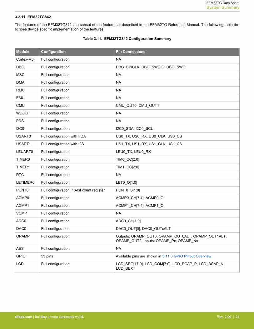
3.2.11 EFM32TG842
The features of the EFM32TG842 is a subset of the feature set described in the EFM32TG Reference Manual. The following table de-scribes device specific implementation of the features.
Table 3.11. EFM32TG842 Configuration Summary
Module Configuration Pin Connections
Cortex-M3 Full configuration NA
DBG Full configuration DBG_SWCLK, DBG_SWDIO, DBG_SWO
MSC Full configuration NA
DMA Full configuration NA
RMU Full configuration NA
EMU Full configuration NA
CMU Full configuration CMU_OUT0, CMU_OUT1
WDOG Full configuration NA
PRS Full configuration NA
I2C0 Full configuration I2C0_SDA, I2C0_SCL
USART0 Full configuration with IrDA US0_TX, US0_RX. US0_CLK, US0_CS
USART1 Full configuration with I2S US1_TX, US1_RX, US1_CLK, US1_CS
LEUART0 Full configuration LEU0_TX, LEU0_RX
TIMER0 Full configuration TIM0_CC[2:0]
TIMER1 Full configuration TIM1_CC[2:0]
RTC Full configuration NA
LETIMER0 Full configuration LET0_O[1:0]
PCNT0 Full configuration, 16-bit count register PCNT0_S[1:0]
ACMP0 Full configuration ACMP0_CH[7:4], ACMP0_O
ACMP1 Full configuration ACMP1_CH[7:4], ACMP1_O
VCMP Full configuration NA
ADC0 Full configuration ADC0_CH[7:0]
DAC0 Full configuration DAC0_OUT[0], DAC0_OUTxALT
OPAMP Full configuration Outputs: OPAMP_OUT0, OPAMP_OUT0ALT, OPAMP_OUT1ALT,OPAMP_OUT2, Inputs: OPAMP_Px, OPAMP_Nx
AES Full configuration NA
GPIO 53 pins Available pins are shown in 5.11.3 GPIO Pinout Overview
LCD Full configuration LCD_SEG[17:0], LCD_COM[7:0], LCD_BCAP_P, LCD_BCAP_N,LCD_BEXT
EFM32TG Data SheetSystem Summary
silabs.com | Building a more connected world. Rev. 2.00 | 25
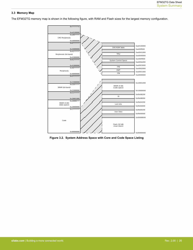
3.3 Memory Map
The EFM32TG memory map is shown in the following figure, with RAM and Flash sizes for the largest memory configuration.
Figure 3.2. System Address Space with Core and Code Space Listing
EFM32TG Data SheetSystem Summary
silabs.com | Building a more connected world. Rev. 2.00 | 26
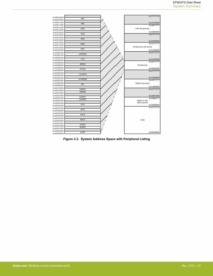
Figure 3.3. System Address Space with Peripheral Listing
EFM32TG Data SheetSystem Summary
silabs.com | Building a more connected world. Rev. 2.00 | 27
4. Electrical Characteristics
4.1 Test Conditions
4.1.1 Typical Values
The typical data are based on TAMB=25°C and VDD=3.0 V, as defined in 4.3 General Operating Conditions, unless otherwise specified.
4.1.2 Minimum and Maximum Values
The minimum and maximum values represent the worst conditions of ambient temperature, supply voltage and frequencies, as definedin 4.3 General Operating Conditions, unless otherwise specified.
4.2 Absolute Maximum Ratings
The absolute maximum ratings are stress ratings, and functional operation under such conditions are not guaranteed. Stress beyondthe limits specified in the following table may affect the device reliability or cause permanent damage to the device. Functional operat-ing conditions are given in 4.3 General Operating Conditions.
Table 4.1. Absolute Maximum Ratings
Parameter Symbol Test Condition Min Typ Max Unit
Storage temperature range TSTG -40 — 1501 °C
Maximum soldering temperature TS Latest IPC/JEDEC J-STD-020 Standard
— — 260 °C
External main supply voltage VDDMAX 0 — 3.8 V
Voltage on any I/O pin VIOPIN -0.3 — VDD+0.3 V
Note:1. Based on programmed devices tested for 10000 hours at 150°C. Storage temperature affects retention of preprogrammed cali-
bration values stored in flash. Please refer to the Flash section in the Electrical Characteristics for information on flash data reten-tion for different temperatures.
4.3 General Operating Conditions
Table 4.2. General Operating Conditions
Parameter Symbol Min Typ Max Unit
Ambient temperature range TAMB -40 — 85 °C
Operating supply voltage VDDOP 1.98 — 3.8 V
Internal APB clock frequency fAPB — — 32 MHz
Internal AHB clock frequency fAHB — — 32 MHz
EFM32TG Data SheetElectrical Characteristics
silabs.com | Building a more connected world. Rev. 2.00 | 28
4.4 Current Consumption
Table 4.3. Current Consumption
Parameter Symbol Test Condition Min Typ Max Unit
EM0 current. No prescaling.Running prime number calcula-tion code from Flash. (Produc-tion test condition = 14 MHz)
IEM0
32 MHz HFXO, all peripheral clocks disa-bled, VDD= 3.0 V
— 157 — µA/MHz
28 MHz HFRCO, all peripheral clocks disa-bled, VDD= 3.0 V
— 150 170 µA/MHz
21 MHz HFRCO, all peripheral clocks disa-bled, VDD= 3.0 V
— 153 172 µA/MHz
14 MHz HFRCO, all peripheral clocks disa-bled, VDD= 3.0 V
— 155 175 µA/MHz
11 MHz HFRCO, all peripheral clocks disa-bled, VDD= 3.0 V
— 157 178 µA/MHz
6.6 MHz HFRCO, all peripheral clocks disa-bled, VDD= 3.0 V
— 162 183 µA/MHz
1.2 MHz HFRCO, all peripheral clocks disa-bled, VDD= 3.0 V
— 200 240 µA/MHz
EM1 current (Production testcondition = 14 MHz)
IEM1
32 MHz HFXO, all peripheral clocks disa-bled, VDD= 3.0 V
— 53 — µA/MHz
28 MHz HFRCO, all peripheral clocks disa-bled, VDD= 3.0 V
— 51 57 µA/MHz
21 MHz HFRCO, all peripheral clocks disa-bled, VDD= 3.0 V
— 55 59 µA/MHz
14 MHz HFRCO, all peripheral clocks disa-bled, VDD= 3.0 V
— 56 61 µA/MHz
11 MHz HFRCO, all peripheral clocks disa-bled, VDD= 3.0 V
— 58 63 µA/MHz
6.6 MHz HFRCO, all peripheral clocks disa-bled, VDD= 3.0 V
— 63 68 µA/MHz
1.2 MHz HFRCO. all peripheral clocks disa-bled, VDD= 3.0 V
— 100 122 µA/MHz
EM2 current IEM2
EM2 current with RTC prescaled to 1 Hz,32.768 kHz LFRCO, VDD= 3.0 V,TAMB=25ºC
— 1.0 1.2 µA
EM2 current with RTC prescaled to 1 Hz,32.768 kHz LFRCO, VDD= 3.0 V,TAMB=85ºC
— 2.4 5.0 µA
EM3 current IEM3VDD= 3.0 V, TAMB=25ºC — 0.59 1.0 µA
VDD= 3.0 V, TAMB=85ºC — 2.0 4.5 µA
EM4 current IEM4VDD= 3.0 V, TAMB=25ºC — 0.02 0.055 µA
VDD= 3.0 V, TAMB=85ºC — 0.25 0.70 µA
EFM32TG Data SheetElectrical Characteristics
silabs.com | Building a more connected world. Rev. 2.00 | 29
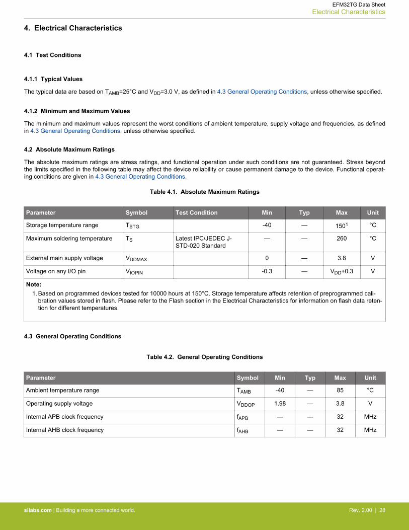
4.4.1 EM2 Current Consumption
Figure 4.1. EM2 Current Consumption, RTC prescaled to 1 kHz, 32.768 kHz LFRCO
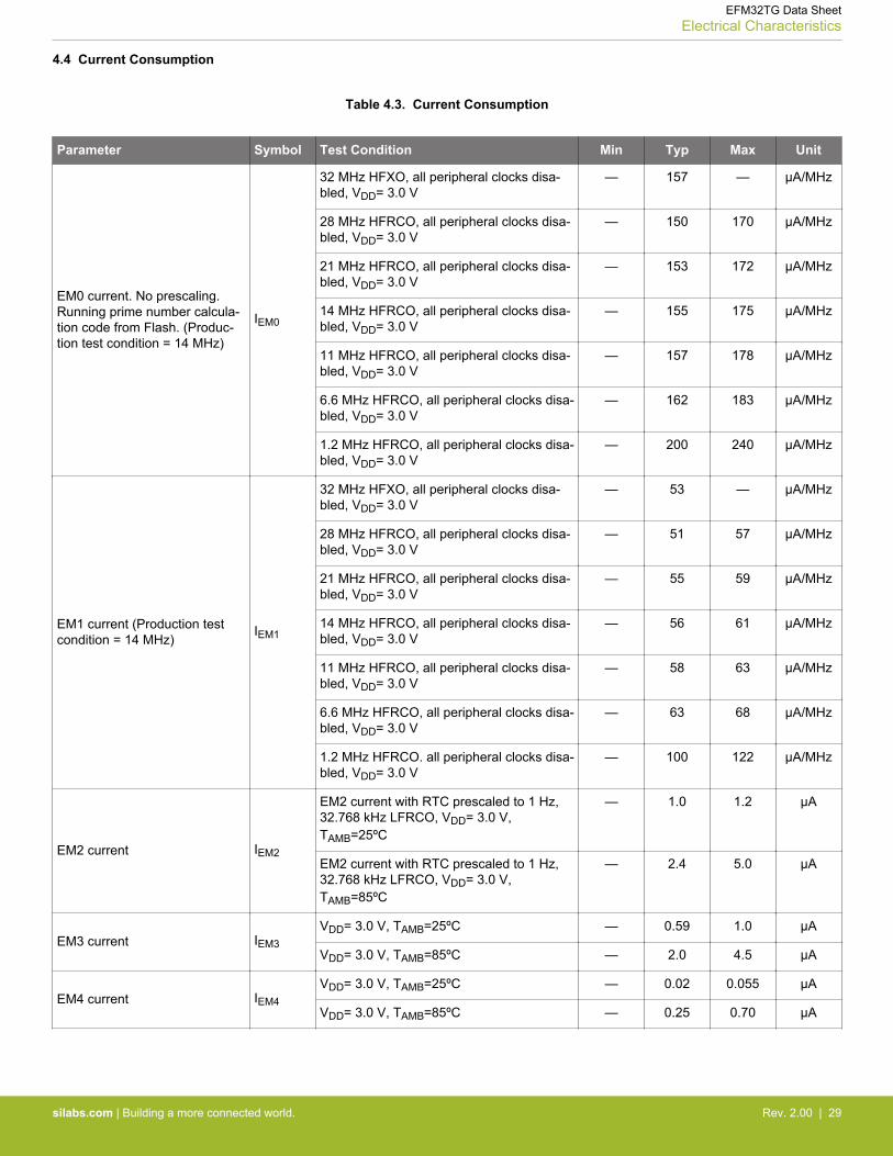
4.4.2 EM3 Current Consumption
Figure 4.2. EM3 Current Consumption
EFM32TG Data SheetElectrical Characteristics
silabs.com | Building a more connected world. Rev. 2.00 | 30
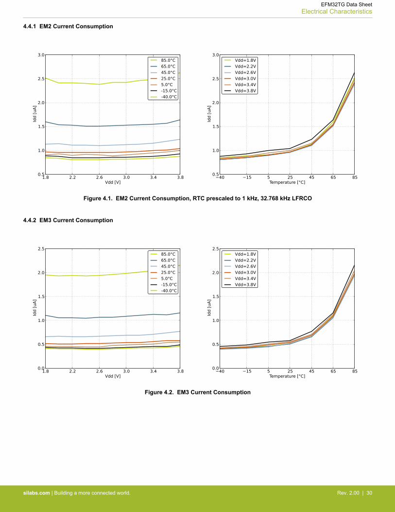
4.4.3 EM4 Current Consumption
Figure 4.3. EM4 Current Consumption
4.5 Transition between Energy Modes
The transition times are measured from the trigger to the first clock edge in the CPU.
Table 4.4. Energy Modes Transitions
Parameter Symbol Min Typ Max Unit
Transition time from EM1 to EM0 tEM10 — 0 — HFCORECLK cycles
Transition time from EM2 to EM0 tEM20 — 2 — µs
Transition time from EM3 to EM0 tEM30 — 2 — µs
Transition time from EM4 to EM0 tEM40 — 163 — µs
EFM32TG Data SheetElectrical Characteristics
silabs.com | Building a more connected world. Rev. 2.00 | 31
4.6 Power Management
The EFM32TG requires the AVDD_x, VDD_DREG and IOVDD_x pins to be connected together (with optional filter) at the PCB level.For practical schematic recommendations, please see the application note, AN0002 EFM32 Hardware Design Considerations.
Table 4.5. Power Management
Parameter Symbol Test Condition Min Typ Max Unit
BOD threshold on falling exter-nal supply voltage
VBODextthr- 1.74 — 1.96 V
BOD threshold on rising exter-nal supply voltage
VBODextthr+ — 1.85 1.98 V
Power-on Reset (POR) thresh-old on rising external supplyvoltage
VPORthr+ — — 1.98 V
Delay from reset is released un-til program execution starts
tRESET Applies to Power-on Reset, Brown-out Reset and pin reset.
— 163 — µs
Voltage regulator decouplingcapacitor.
CDECOUPLE X5R capacitor recommended. Applybetween DECOUPLE pin andGROUND
— 1 — µF
4.7 Flash
Table 4.6. Flash
Parameter Symbol Test Condition Min Typ Max Unit
Flash erase cycles before fail-ure
ECFLASH 20000 — — cycles
Flash data retention RETFLASH
TAMB<150ºC 10000 — — h
TAMB<85ºC 10 — — years
TAMB<70ºC 20 — — years
Word (32-bit) programming time tW_PROG 20 — — µs
Page erase time tP_ERASE 20 20.4 20.8 ms
Device erase time tD_ERASE 40 40.8 41.6 ms
Erase current IERASE — — 71 mA
Write current IWRITE — — 71 mA
Supply voltage during flasherase and write
VFLASH 1.98 — 3.8 V
Note:1. Measured at 25°C
EFM32TG Data SheetElectrical Characteristics
silabs.com | Building a more connected world. Rev. 2.00 | 32
4.8 General Purpose Input Output
Table 4.7. GPIO
Parameter Symbol Test Condition Min Typ Max Unit
Input low voltage VIOIL — — 0.30×VDD V
Input high voltage VIOIH 0.70×VDD — — V
Output high voltage (Produc-tion test condition = 3.0V,DRIVEMODE = STANDARD)
VIOOH
Sourcing 0.1 mA, VDD=1.98 V,GPIO_Px_CTRL DRIVEMODE = LOW-EST
— 0.80×VDD — V
Sourcing 0.1 mA, VDD=3.0 V,GPIO_Px_CTRL DRIVEMODE = LOW-EST
— 0.90×VDD — V
Sourcing 1 mA, VDD=1.98 V,GPIO_Px_CTRL DRIVEMODE = LOW
— 0.85×VDD — V
Sourcing 1 mA, VDD=3.0 V,GPIO_Px_CTRL DRIVEMODE = LOW
— 0.90×VDD — V
Sourcing 6 mA, VDD=1.98 V,GPIO_Px_CTRL DRIVEMODE =STANDARD
0.75×VDD — — V
Sourcing 6 mA, VDD=3.0 V,GPIO_Px_CTRL DRIVEMODE =STANDARD
0.85×VDD — — V
Sourcing 20 mA, VDD=1.98 V,GPIO_Px_CTRL DRIVEMODE = HIGH
0.60×VDD — — V
Sourcing 20 mA, VDD=3.0 V,GPIO_Px_CTRL DRIVEMODE = HIGH
0.80×VDD — — V
Output low voltage (Produc-tion test condition = 3.0V,DRIVEMODE = STANDARD)
VIOOL
Sinking 0.1 mA, VDD=1.98 V,GPIO_Px_CTRL DRIVEMODE = LOW-EST
— 0.20×VDD — V
Sinking 0.1 mA, VDD=3.0 V,GPIO_Px_CTRL DRIVEMODE = LOW-EST
— 0.10×VDD — V
Sinking 1 mA, VDD=1.98 V,GPIO_Px_CTRL DRIVEMODE = LOW
— 0.10×VDD — V
Sinking 1 mA, VDD=3.0 V,GPIO_Px_CTRL DRIVEMODE = LOW
— 0.05×VDD — V
Sinking 6 mA, VDD=1.98 V,GPIO_Px_CTRL DRIVEMODE =STANDARD
— — 0.30×VDD V
Sinking 6 mA, VDD=3.0 V,GPIO_Px_CTRL DRIVEMODE =STANDARD
— — 0.20×VDD V
Sinking 20 mA, VDD=1.98 V,GPIO_Px_CTRL DRIVEMODE = HIGH
— — 0.35×VDD V
Sinking 20 mA, VDD=3.0 V,GPIO_Px_CTRL DRIVEMODE = HIGH
— — 0.20×VDD V
EFM32TG Data SheetElectrical Characteristics
silabs.com | Building a more connected world. Rev. 2.00 | 33
Parameter Symbol Test Condition Min Typ Max Unit
Input leakage current IIOLEAK High Impedance IO connected toGROUND or VDD
— ±0.1 ±100 nA
I/O pin pull-up resistor RPU — 40 — kΩ
I/O pin pull-down resistor RPD — 40 — kΩ
Internal ESD series resistor RIOESD — 200 — Ω
Pulse width of pulses to be re-moved by the glitch suppres-sion filter
tIO-
GLITCH
10 — 50 ns
Output fall time
tIOOF GPIO_Px_CTRL DRIVEMODE = LOW-EST and load capacitanceCL=12.5-25pF.
20+0.1×CL — 250 ns
GPIO_Px_CTRL DRIVEMODE = LOWand load capacitance CL=350-600pF
20+0.1×CL — 250 ns
I/O pin hysteresis (VIOTHR+ -VIOTHR-)
VIOHYST VDD = 1.98 - 3.8 V 0.1×VDD — — V
EFM32TG Data SheetElectrical Characteristics
silabs.com | Building a more connected world. Rev. 2.00 | 34
0.0 0.5 1.0 1.5 2.0Low-Level Output Voltage [V]
0
1
2
3
4
5
Low
-Lev
el O
utpu
t Cur
rent
[mA
]
-40°C
25°C
85°C
0.0 0.5 1.0 1.5 2.0Low-Level Output Voltage [V]
0
5
10
15
20
Low
-Lev
el O
utpu
t Cur
rent
[mA
]
-40°C
25°C
85°C
0.0 0.5 1.0 1.5 2.0Low-Level Output Voltage [V]
0
5
10
15
20
25
30
35
40
45
Low
-Lev
el O
utpu
t Cur
rent
[mA
]
-40°C
25°C
85°C
0.0 0.5 1.0 1.5 2.0Low-Level Output Voltage [V]
0.00
0.05
0.10
0.15
0.20
Low
-Lev
el O
utpu
t Cur
rent
[mA
]
-40°C
25°C
85°C
GPIO_Px_CTRL DRIVEMODE = LOWEST GPIO_Px_CTRL DRIVEMODE = LOW
GPIO_Px_CTRL DRIVEMODE = STANDARD GPIO_Px_CTRL DRIVEMODE = HIGH
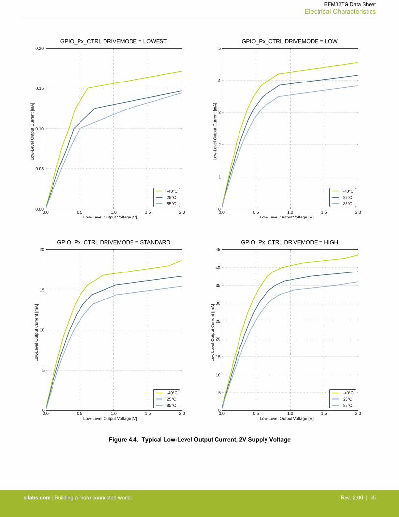
Figure 4.4. Typical Low-Level Output Current, 2V Supply Voltage
EFM32TG Data SheetElectrical Characteristics
silabs.com | Building a more connected world. Rev. 2.00 | 35
0.0 0.5 1.0 1.5 2.0High-Level Output Voltage [V]
–20
–15
–10
–5
0
Hig
h-Le
vel O
utpu
t Cur
rent
[mA
]
-40°C
25°C
85°C
0.0 0.5 1.0 1.5 2.0High-Level Output Voltage [V]
–50
–40
–30
–20
–10
0
Hig
h-Le
vel O
utpu
t Cur
rent
[mA
]
-40°C
25°C
85°C
0.0 0.5 1.0 1.5 2.0High-Level Output Voltage [V]
–0.20
–0.15
–0.10
–0.05
0.00
Hig
h-Le
vel O
utpu
t Cur
rent
[mA
]
-40°C
25°C
85°C
0.0 0.5 1.0 1.5 2.0High-Level Output Voltage [V]
–2.5
–2.0
–1.5
–1.0
–0.5
0.0
Hig
h-Le
vel O
utpu
t Cur
rent
[mA
]
-40°C
25°C
85°C
GPIO_Px_CTRL DRIVEMODE = LOWEST GPIO_Px_CTRL DRIVEMODE = LOW
GPIO_Px_CTRL DRIVEMODE = STANDARD GPIO_Px_CTRL DRIVEMODE = HIGH
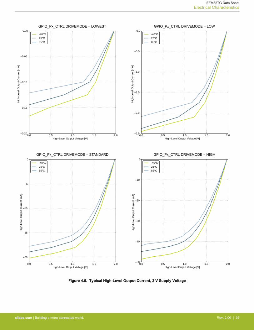
Figure 4.5. Typical High-Level Output Current, 2 V Supply Voltage
EFM32TG Data SheetElectrical Characteristics
silabs.com | Building a more connected world. Rev. 2.00 | 36
0.0 0.5 1.0 1.5 2.0 2.5 3.0Low-Level Output Voltage [V]
0.0
0.1
0.2
0.3
0.4
0.5
Low
-Lev
el O
utpu
t Cur
rent
[mA
]
-40°C
25°C
85°C
0.0 0.5 1.0 1.5 2.0 2.5 3.0Low-Level Output Voltage [V]
0
2
4
6
8
10
Low
-Lev
el O
utpu
t Cur
rent
[mA
]
-40°C
25°C
85°C
0.0 0.5 1.0 1.5 2.0 2.5 3.0Low-Level Output Voltage [V]
0
5
10
15
20
25
30
35
40
Low
-Lev
el O
utpu
t Cur
rent
[mA
]
-40°C
25°C
85°C
0.0 0.5 1.0 1.5 2.0 2.5 3.0Low-Level Output Voltage [V]
0
10
20
30
40
50
Low
-Lev
el O
utpu
t Cur
rent
[mA
]
-40°C
25°C
85°C
GPIO_Px_CTRL DRIVEMODE = LOWEST GPIO_Px_CTRL DRIVEMODE = LOW
GPIO_Px_CTRL DRIVEMODE = STANDARD GPIO_Px_CTRL DRIVEMODE = HIGH
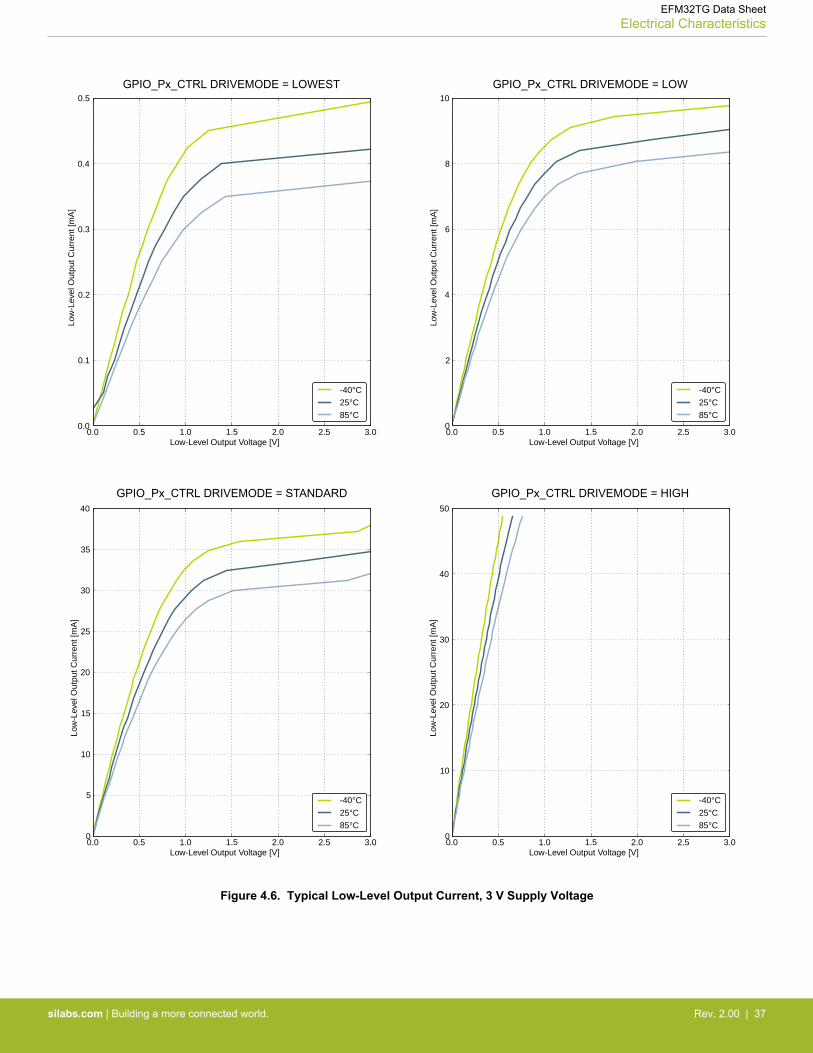
Figure 4.6. Typical Low-Level Output Current, 3 V Supply Voltage
EFM32TG Data SheetElectrical Characteristics
silabs.com | Building a more connected world. Rev. 2.00 | 37
0.0 0.5 1.0 1.5 2.0 2.5 3.0High-Level Output Voltage [V]
–50
–40
–30
–20
–10
0
Hig
h-Le
vel O
utpu
t Cur
rent
[mA
]
-40°C
25°C
85°C
0.0 0.5 1.0 1.5 2.0 2.5 3.0High-Level Output Voltage [V]
–50
–40
–30
–20
–10
0
Hig
h-Le
vel O
utpu
t Cur
rent
[mA
]
-40°C
25°C
85°C
0.0 0.5 1.0 1.5 2.0 2.5 3.0High-Level Output Voltage [V]
–0.5
–0.4
–0.3
–0.2
–0.1
0.0
Hig
h-Le
vel O
utpu
t Cur
rent
[mA
]
-40°C
25°C
85°C
0.0 0.5 1.0 1.5 2.0 2.5 3.0High-Level Output Voltage [V]
–6
–5
–4
–3
–2
–1
0
Hig
h-Le
vel O
utpu
t Cur
rent
[mA
]
-40°C
25°C
85°C
GPIO_Px_CTRL DRIVEMODE = LOWEST GPIO_Px_CTRL DRIVEMODE = LOW
GPIO_Px_CTRL DRIVEMODE = STANDARD GPIO_Px_CTRL DRIVEMODE = HIGH
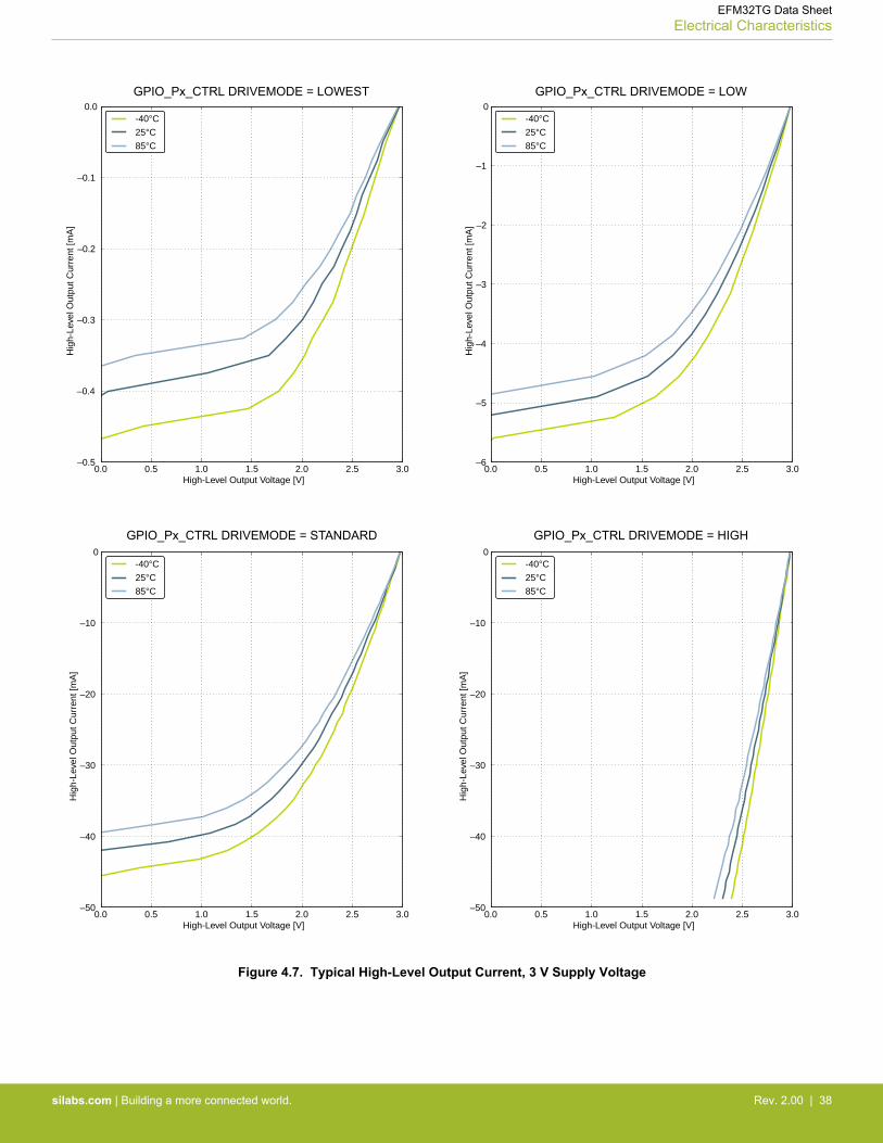
Figure 4.7. Typical High-Level Output Current, 3 V Supply Voltage
EFM32TG Data SheetElectrical Characteristics
silabs.com | Building a more connected world. Rev. 2.00 | 38
0.0 0.5 1.0 1.5 2.0 2.5 3.0 3.5Low-Level Output Voltage [V]
0.0
0.1
0.2
0.3
0.4
0.5
0.6
0.7
0.8
Low
-Lev
el O
utpu
t Cur
rent
[mA
]
-40°C
25°C
85°C
0.0 0.5 1.0 1.5 2.0 2.5 3.0 3.5Low-Level Output Voltage [V]
0
2
4
6
8
10
12
14
Low
-Lev
el O
utpu
t Cur
rent
[mA
]
-40°C
25°C
85°C
0.0 0.5 1.0 1.5 2.0 2.5 3.0 3.5Low-Level Output Voltage [V]
0
10
20
30
40
50
Low
-Lev
el O
utpu
t Cur
rent
[mA
]
-40°C
25°C
85°C
0.0 0.5 1.0 1.5 2.0 2.5 3.0 3.5Low-Level Output Voltage [V]
0
10
20
30
40
50
Low
-Lev
el O
utpu
t Cur
rent
[mA
]
-40°C
25°C
85°C
GPIO_Px_CTRL DRIVEMODE = LOWEST GPIO_Px_CTRL DRIVEMODE = LOW
GPIO_Px_CTRL DRIVEMODE = STANDARD GPIO_Px_CTRL DRIVEMODE = HIGH
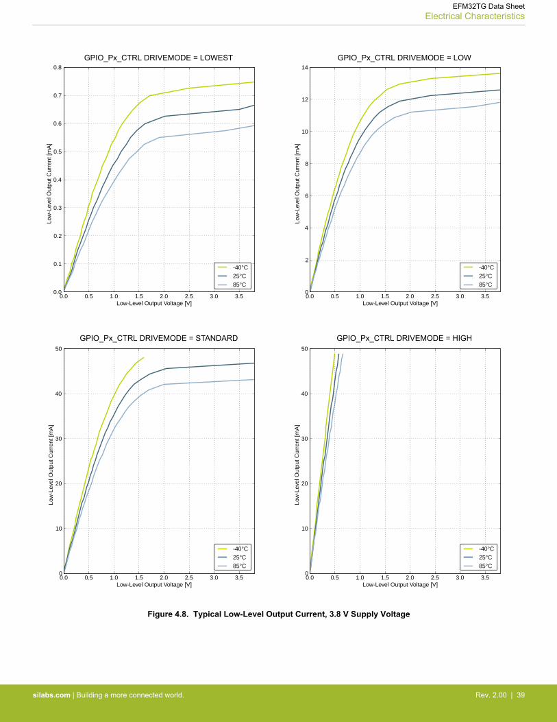
Figure 4.8. Typical Low-Level Output Current, 3.8 V Supply Voltage
EFM32TG Data SheetElectrical Characteristics
silabs.com | Building a more connected world. Rev. 2.00 | 39
0.0 0.5 1.0 1.5 2.0 2.5 3.0 3.5High-Level Output Voltage [V]
–0.8
–0.7
–0.6
–0.5
–0.4
–0.3
–0.2
–0.1
0.0
Hig
h-Le
vel O
utpu
t Cur
rent
[mA
]
-40°C
25°C
85°C
0.0 0.5 1.0 1.5 2.0 2.5 3.0 3.5High-Level Output Voltage [V]
–9
–8
–7
–6
–5
–4
–3
–2
–1
0
Hig
h-Le
vel O
utpu
t Cur
rent
[mA
]
-40°C
25°C
85°C
0.0 0.5 1.0 1.5 2.0 2.5 3.0 3.5High-Level Output Voltage [V]
–50
–40
–30
–20
–10
0
Hig
h-Le
vel O
utpu
t Cur
rent
[mA
]
-40°C
25°C
85°C
0.0 0.5 1.0 1.5 2.0 2.5 3.0 3.5High-Level Output Voltage [V]
–50
–40
–30
–20
–10
0
Hig
h-Le
vel O
utpu
t Cur
rent
[mA
]
-40°C
25°C
85°C
GPIO_Px_CTRL DRIVEMODE = LOWEST GPIO_Px_CTRL DRIVEMODE = LOW
GPIO_Px_CTRL DRIVEMODE = STANDARD GPIO_Px_CTRL DRIVEMODE = HIGH
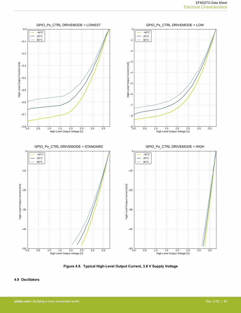
Figure 4.9. Typical High-Level Output Current, 3.8 V Supply Voltage
4.9 Oscillators
EFM32TG Data SheetElectrical Characteristics
silabs.com | Building a more connected world. Rev. 2.00 | 40
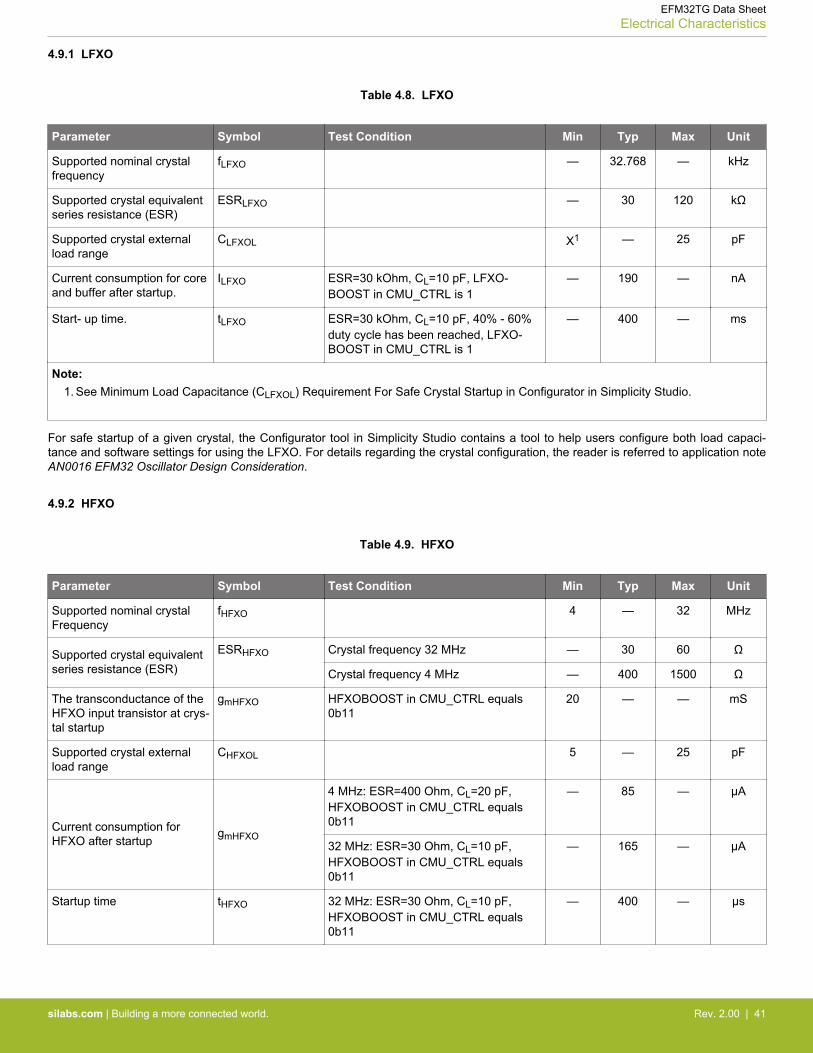
4.9.1 LFXO
Table 4.8. LFXO
Parameter Symbol Test Condition Min Typ Max Unit
Supported nominal crystalfrequency
fLFXO — 32.768 — kHz
Supported crystal equivalentseries resistance (ESR)
ESRLFXO — 30 120 kΩ
Supported crystal externalload range
CLFXOL X1 — 25 pF
Current consumption for coreand buffer after startup.
ILFXO ESR=30 kOhm, CL=10 pF, LFXO-BOOST in CMU_CTRL is 1
— 190 — nA
Start- up time. tLFXO ESR=30 kOhm, CL=10 pF, 40% - 60%duty cycle has been reached, LFXO-BOOST in CMU_CTRL is 1
— 400 — ms
Note:1. See Minimum Load Capacitance (CLFXOL) Requirement For Safe Crystal Startup in Configurator in Simplicity Studio.
For safe startup of a given crystal, the Configurator tool in Simplicity Studio contains a tool to help users configure both load capaci-tance and software settings for using the LFXO. For details regarding the crystal configuration, the reader is referred to application noteAN0016 EFM32 Oscillator Design Consideration.
4.9.2 HFXO
Table 4.9. HFXO
Parameter Symbol Test Condition Min Typ Max Unit
Supported nominal crystalFrequency
fHFXO 4 — 32 MHz
Supported crystal equivalentseries resistance (ESR)
ESRHFXO Crystal frequency 32 MHz — 30 60 Ω
Crystal frequency 4 MHz — 400 1500 Ω
The transconductance of theHFXO input transistor at crys-tal startup
gmHFXO HFXOBOOST in CMU_CTRL equals0b11
20 — — mS
Supported crystal externalload range
CHFXOL 5 — 25 pF
Current consumption forHFXO after startup
gmHFXO
4 MHz: ESR=400 Ohm, CL=20 pF,HFXOBOOST in CMU_CTRL equals0b11
— 85 — µA
32 MHz: ESR=30 Ohm, CL=10 pF,HFXOBOOST in CMU_CTRL equals0b11
— 165 — µA
Startup time tHFXO 32 MHz: ESR=30 Ohm, CL=10 pF,HFXOBOOST in CMU_CTRL equals0b11
— 400 — µs
EFM32TG Data SheetElectrical Characteristics
silabs.com | Building a more connected world. Rev. 2.00 | 41
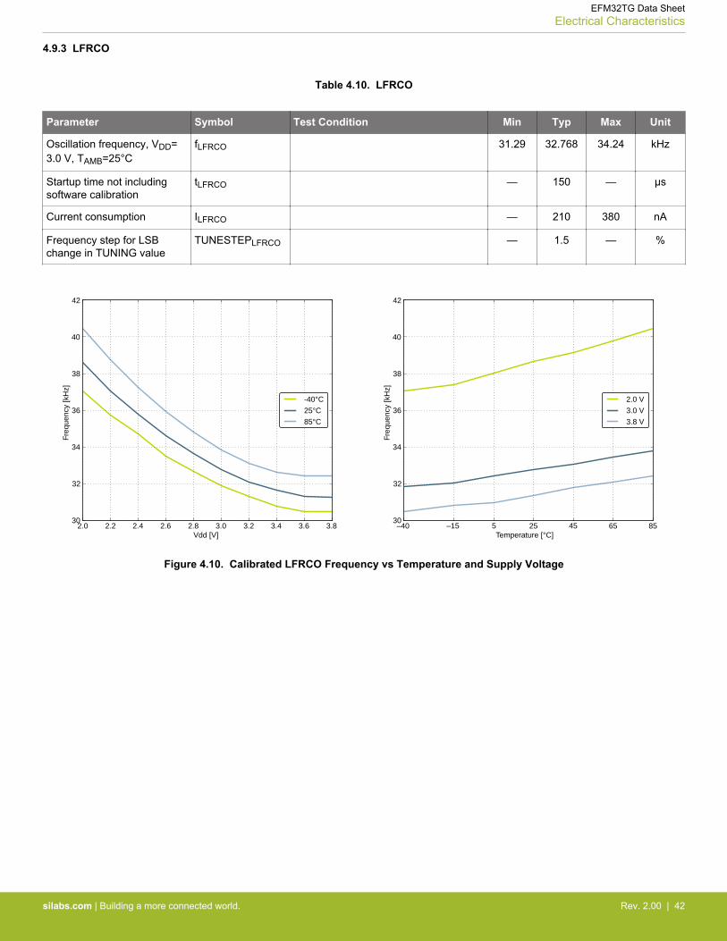
4.9.3 LFRCO
Table 4.10. LFRCO
Parameter Symbol Test Condition Min Typ Max Unit
Oscillation frequency, VDD=3.0 V, TAMB=25°C
fLFRCO 31.29 32.768 34.24 kHz
Startup time not includingsoftware calibration
tLFRCO — 150 — µs
Current consumption ILFRCO — 210 380 nA
Frequency step for LSBchange in TUNING value
TUNESTEPLFRCO — 1.5 — %
–40 –15 5 25 45 65 85Temperature [°C]
30
32
34
36
38
40
42
Freq
uenc
y [k
Hz]
2.0 V
3.0 V
3.8 V
2.0 2.2 2.4 2.6 2.8 3.0 3.2 3.4 3.6 3.8Vdd [V]
30
32
34
36
38
40
42
Freq
uenc
y [k
Hz]
-40°C
25°C
85°C
Figure 4.10. Calibrated LFRCO Frequency vs Temperature and Supply Voltage
EFM32TG Data SheetElectrical Characteristics
silabs.com | Building a more connected world. Rev. 2.00 | 42
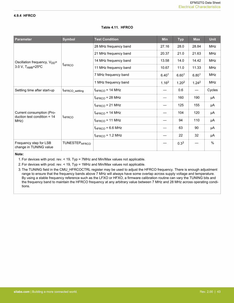
4.9.4 HFRCO
Table 4.11. HFRCO
Parameter Symbol Test Condition Min Typ Max Unit
Oscillation frequency, VDD=3.0 V, TAMB=25ºC
fHFRCO
28 MHz frequency band 27.16 28.0 28.84 MHz
21 MHz frequency band 20.37 21.0 21.63 MHz
14 MHz frequency band 13.58 14.0 14.42 MHz
11 MHz frequency band 10.67 11.0 11.33 MHz
7 MHz frequency band 6.401 6.601 6.801 MHz
1 MHz frequency band 1.162 1.202 1.242 MHz
Settling time after start-up tHFRCO_settling fHFRCO = 14 MHz — 0.6 — Cycles
Current consumption (Pro-duction test condition = 14MHz)
IHFRCO
fHFRCO = 28 MHz — 160 190 µA
fHFRCO = 21 MHz — 125 155 µA
fHFRCO = 14 MHz — 104 120 µA
fHFRCO = 11 MHz — 94 110 µA
fHFRCO = 6.6 MHz — 63 90 µA
fHFRCO = 1.2 MHz — 22 32 µA
Frequency step for LSBchange in TUNING value
TUNESTEPHFRCO — 0.33 — %
Note:1. For devices with prod. rev. < 19, Typ = 7MHz and Min/Max values not applicable.2. For devices with prod. rev. < 19, Typ = 1MHz and Min/Max values not applicable.3. The TUNING field in the CMU_HFRCOCTRL register may be used to adjust the HFRCO frequency. There is enough adjustment
range to ensure that the frequency bands above 7 MHz will always have some overlap across supply voltage and temperature.By using a stable frequency reference such as the LFXO or HFXO, a firmware calibration routine can vary the TUNING bits andthe frequency band to maintain the HFRCO frequency at any arbitrary value between 7 MHz and 28 MHz across operating condi-tions.
EFM32TG Data SheetElectrical Characteristics
silabs.com | Building a more connected world. Rev. 2.00 | 43
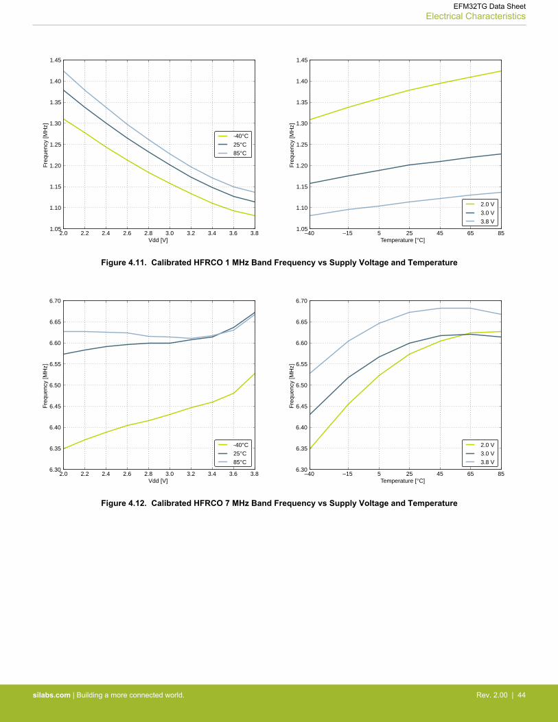
2.0 2.2 2.4 2.6 2.8 3.0 3.2 3.4 3.6 3.8Vdd [V]
1.05
1.10
1.15
1.20
1.25
1.30
1.35
1.40
1.45
Freq
uenc
y [M
Hz]
-40°C
25°C
85°C
–40 –15 5 25 45 65 85Temperature [°C]
1.05
1.10
1.15
1.20
1.25
1.30
1.35
1.40
1.45
Freq
uenc
y [M
Hz]
2.0 V
3.0 V
3.8 V
Figure 4.11. Calibrated HFRCO 1 MHz Band Frequency vs Supply Voltage and Temperature
2.0 2.2 2.4 2.6 2.8 3.0 3.2 3.4 3.6 3.8Vdd [V]
6.30
6.35
6.40
6.45
6.50
6.55
6.60
6.65
6.70
Freq
uenc
y [M
Hz]
-40°C
25°C
85°C
–40 –15 5 25 45 65 85Temperature [°C]
6.30
6.35
6.40
6.45
6.50
6.55
6.60
6.65
6.70
Freq
uenc
y [M
Hz]
2.0 V
3.0 V
3.8 V
Figure 4.12. Calibrated HFRCO 7 MHz Band Frequency vs Supply Voltage and Temperature
EFM32TG Data SheetElectrical Characteristics
silabs.com | Building a more connected world. Rev. 2.00 | 44
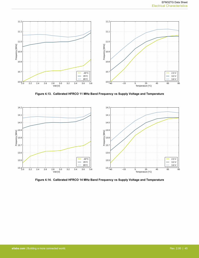
2.0 2.2 2.4 2.6 2.8 3.0 3.2 3.4 3.6 3.8Vdd [V]
10.6
10.7
10.8
10.9
11.0
11.1
11.2
Freq
uenc
y [M
Hz]
-40°C
25°C
85°C
–40 –15 5 25 45 65 85Temperature [°C]
10.6
10.7
10.8
10.9
11.0
11.1
11.2
Freq
uenc
y [M
Hz]
2.0 V
3.0 V
3.8 V
Figure 4.13. Calibrated HFRCO 11 MHz Band Frequency vs Supply Voltage and Temperature
2.0 2.2 2.4 2.6 2.8 3.0 3.2 3.4 3.6 3.8Vdd [V]
13.4
13.5
13.6
13.7
13.8
13.9
14.0
14.1
14.2
Freq
uenc
y [M
Hz]
-40°C
25°C
85°C
–40 –15 5 25 45 65 85Temperature [°C]
13.4
13.5
13.6
13.7
13.8
13.9
14.0
14.1
14.2
Freq
uenc
y [M
Hz]
2.0 V
3.0 V
3.8 V
Figure 4.14. Calibrated HFRCO 14 MHz Band Frequency vs Supply Voltage and Temperature
EFM32TG Data SheetElectrical Characteristics
silabs.com | Building a more connected world. Rev. 2.00 | 45
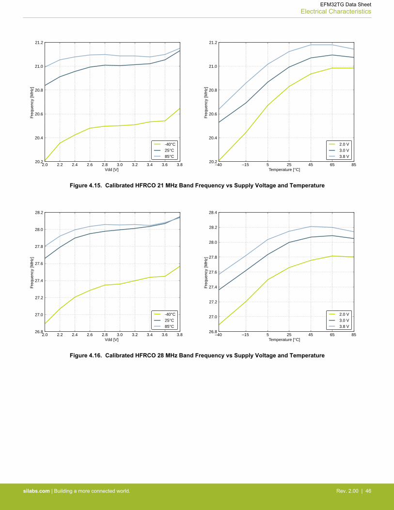
2.0 2.2 2.4 2.6 2.8 3.0 3.2 3.4 3.6 3.8Vdd [V]
20.2
20.4
20.6
20.8
21.0
21.2
Freq
uenc
y [M
Hz]
-40°C
25°C
85°C
–40 –15 5 25 45 65 85Temperature [°C]
20.2
20.4
20.6
20.8
21.0
21.2
Freq
uenc
y [M
Hz]
2.0 V
3.0 V
3.8 V
Figure 4.15. Calibrated HFRCO 21 MHz Band Frequency vs Supply Voltage and Temperature
2.0 2.2 2.4 2.6 2.8 3.0 3.2 3.4 3.6 3.8Vdd [V]
26.8
27.0
27.2
27.4
27.6
27.8
28.0
28.2
Freq
uenc
y [M
Hz]
-40°C
25°C
85°C
–40 –15 5 25 45 65 85Temperature [°C]
26.8
27.0
27.2
27.4
27.6
27.8
28.0
28.2
28.4
Freq
uenc
y [M
Hz]
2.0 V
3.0 V
3.8 V
Figure 4.16. Calibrated HFRCO 28 MHz Band Frequency vs Supply Voltage and Temperature
EFM32TG Data SheetElectrical Characteristics
silabs.com | Building a more connected world. Rev. 2.00 | 46
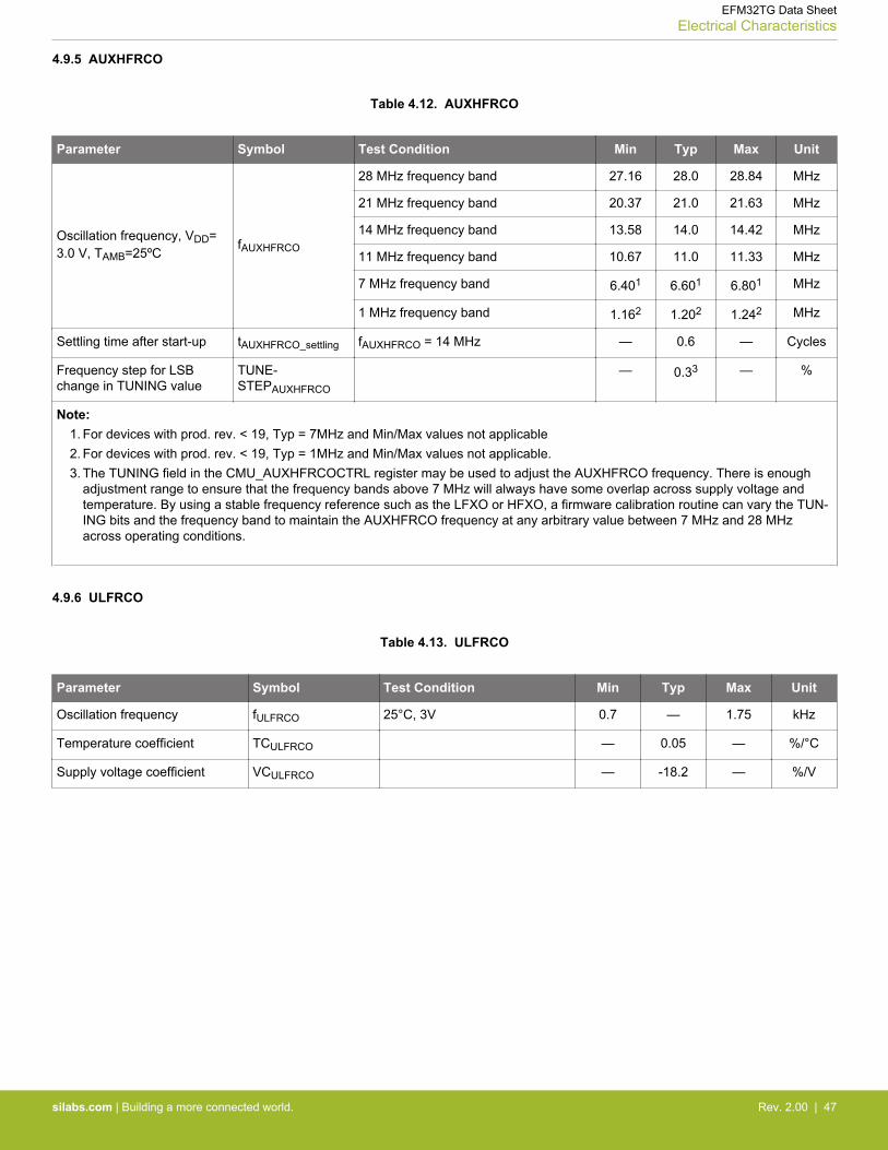
4.9.5 AUXHFRCO
Table 4.12. AUXHFRCO
Parameter Symbol Test Condition Min Typ Max Unit
Oscillation frequency, VDD=3.0 V, TAMB=25ºC
fAUXHFRCO
28 MHz frequency band 27.16 28.0 28.84 MHz
21 MHz frequency band 20.37 21.0 21.63 MHz
14 MHz frequency band 13.58 14.0 14.42 MHz
11 MHz frequency band 10.67 11.0 11.33 MHz
7 MHz frequency band 6.401 6.601 6.801 MHz
1 MHz frequency band 1.162 1.202 1.242 MHz
Settling time after start-up tAUXHFRCO_settling fAUXHFRCO = 14 MHz — 0.6 — Cycles
Frequency step for LSBchange in TUNING value
TUNE-STEPAUXHFRCO
— 0.33 — %
Note:1. For devices with prod. rev. < 19, Typ = 7MHz and Min/Max values not applicable2. For devices with prod. rev. < 19, Typ = 1MHz and Min/Max values not applicable.3. The TUNING field in the CMU_AUXHFRCOCTRL register may be used to adjust the AUXHFRCO frequency. There is enough
adjustment range to ensure that the frequency bands above 7 MHz will always have some overlap across supply voltage andtemperature. By using a stable frequency reference such as the LFXO or HFXO, a firmware calibration routine can vary the TUN-ING bits and the frequency band to maintain the AUXHFRCO frequency at any arbitrary value between 7 MHz and 28 MHzacross operating conditions.
4.9.6 ULFRCO
Table 4.13. ULFRCO
Parameter Symbol Test Condition Min Typ Max Unit
Oscillation frequency fULFRCO 25°C, 3V 0.7 — 1.75 kHz
Temperature coefficient TCULFRCO — 0.05 — %/°C
Supply voltage coefficient VCULFRCO — -18.2 — %/V
EFM32TG Data SheetElectrical Characteristics
silabs.com | Building a more connected world. Rev. 2.00 | 47
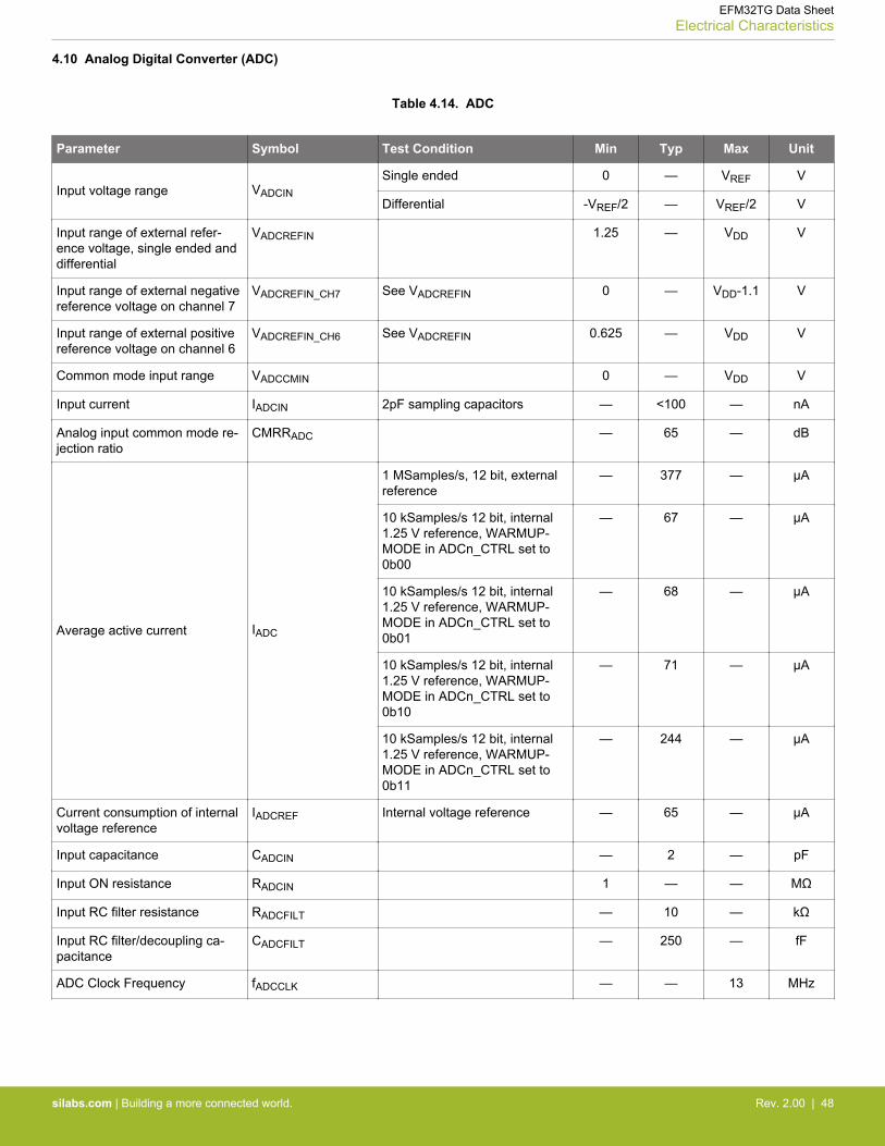
4.10 Analog Digital Converter (ADC)
Table 4.14. ADC
Parameter Symbol Test Condition Min Typ Max Unit
Input voltage range VADCINSingle ended 0 — VREF V
Differential -VREF/2 — VREF/2 V
Input range of external refer-ence voltage, single ended anddifferential
VADCREFIN 1.25 — VDD V
Input range of external negativereference voltage on channel 7
VADCREFIN_CH7 See VADCREFIN 0 — VDD-1.1 V
Input range of external positivereference voltage on channel 6
VADCREFIN_CH6 See VADCREFIN 0.625 — VDD V
Common mode input range VADCCMIN 0 — VDD V
Input current IADCIN 2pF sampling capacitors — <100 — nA
Analog input common mode re-jection ratio
CMRRADC — 65 — dB
Average active current IADC
1 MSamples/s, 12 bit, externalreference
— 377 — µA
10 kSamples/s 12 bit, internal1.25 V reference, WARMUP-MODE in ADCn_CTRL set to0b00
— 67 — µA
10 kSamples/s 12 bit, internal1.25 V reference, WARMUP-MODE in ADCn_CTRL set to0b01
— 68 — µA
10 kSamples/s 12 bit, internal1.25 V reference, WARMUP-MODE in ADCn_CTRL set to0b10
— 71 — µA
10 kSamples/s 12 bit, internal1.25 V reference, WARMUP-MODE in ADCn_CTRL set to0b11
— 244 — µA
Current consumption of internalvoltage reference
IADCREF Internal voltage reference — 65 — µA
Input capacitance CADCIN — 2 — pF
Input ON resistance RADCIN 1 — — MΩ
Input RC filter resistance RADCFILT — 10 — kΩ
Input RC filter/decoupling ca-pacitance
CADCFILT — 250 — fF
ADC Clock Frequency fADCCLK — — 13 MHz
EFM32TG Data SheetElectrical Characteristics
silabs.com | Building a more connected world. Rev. 2.00 | 48
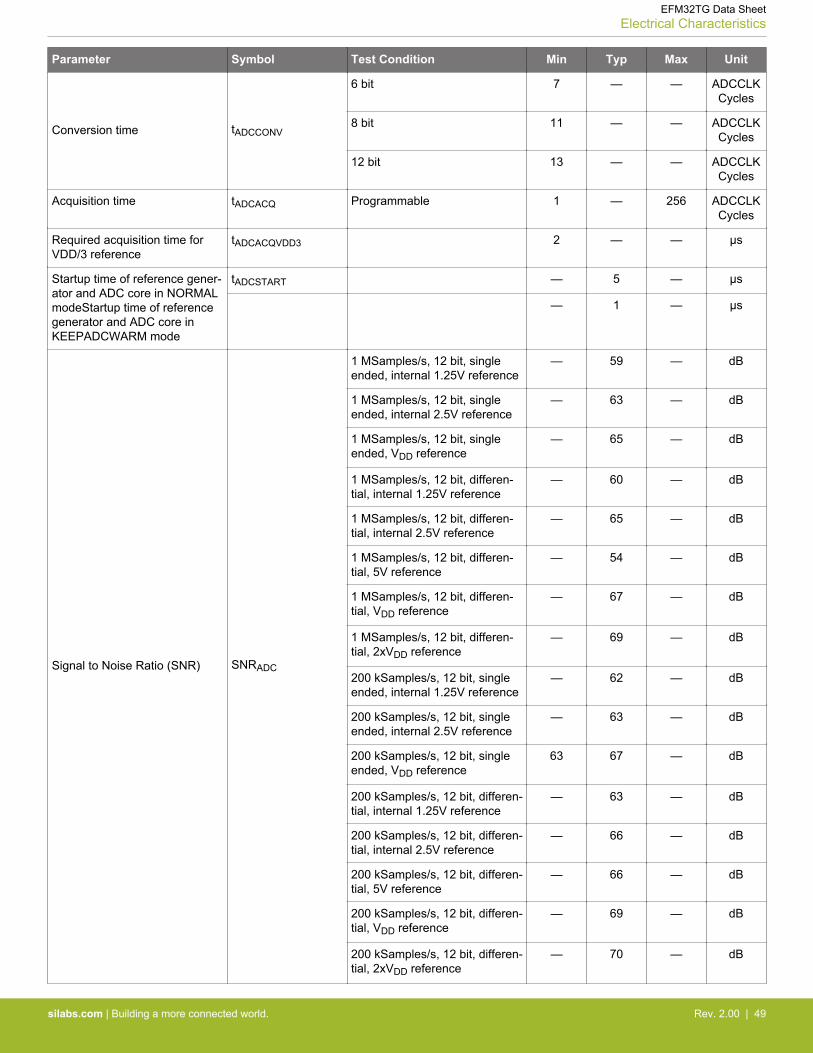
Parameter Symbol Test Condition Min Typ Max Unit
Conversion time tADCCONV
6 bit 7 — — ADCCLKCycles
8 bit 11 — — ADCCLKCycles
12 bit 13 — — ADCCLKCycles
Acquisition time tADCACQ Programmable 1 — 256 ADCCLKCycles
Required acquisition time forVDD/3 reference
tADCACQVDD3 2 — — µs
Startup time of reference gener-ator and ADC core in NORMALmodeStartup time of referencegenerator and ADC core inKEEPADCWARM mode
tADCSTART — 5 — µs
— 1 — µs
Signal to Noise Ratio (SNR) SNRADC
1 MSamples/s, 12 bit, singleended, internal 1.25V reference
— 59 — dB
1 MSamples/s, 12 bit, singleended, internal 2.5V reference
— 63 — dB
1 MSamples/s, 12 bit, singleended, VDD reference
— 65 — dB
1 MSamples/s, 12 bit, differen-tial, internal 1.25V reference
— 60 — dB
1 MSamples/s, 12 bit, differen-tial, internal 2.5V reference
— 65 — dB
1 MSamples/s, 12 bit, differen-tial, 5V reference
— 54 — dB
1 MSamples/s, 12 bit, differen-tial, VDD reference
— 67 — dB
1 MSamples/s, 12 bit, differen-tial, 2xVDD reference
— 69 — dB
200 kSamples/s, 12 bit, singleended, internal 1.25V reference
— 62 — dB
200 kSamples/s, 12 bit, singleended, internal 2.5V reference
— 63 — dB
200 kSamples/s, 12 bit, singleended, VDD reference
63 67 — dB
200 kSamples/s, 12 bit, differen-tial, internal 1.25V reference
— 63 — dB
200 kSamples/s, 12 bit, differen-tial, internal 2.5V reference
— 66 — dB
200 kSamples/s, 12 bit, differen-tial, 5V reference
— 66 — dB
200 kSamples/s, 12 bit, differen-tial, VDD reference
— 69 — dB
200 kSamples/s, 12 bit, differen-tial, 2xVDD reference
— 70 — dB
EFM32TG Data SheetElectrical Characteristics
silabs.com | Building a more connected world. Rev. 2.00 | 49
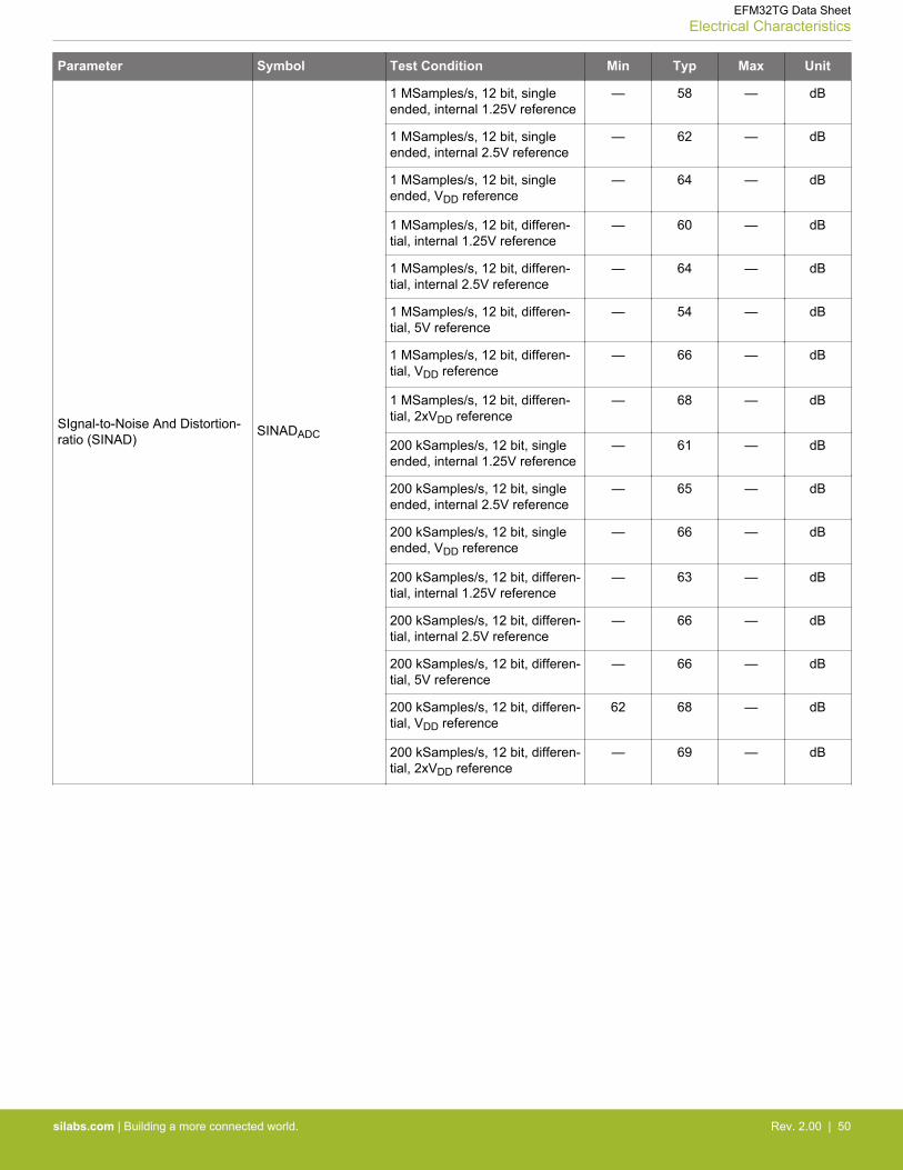
Parameter Symbol Test Condition Min Typ Max Unit
SIgnal-to-Noise And Distortion-ratio (SINAD)
SINADADC
1 MSamples/s, 12 bit, singleended, internal 1.25V reference
— 58 — dB
1 MSamples/s, 12 bit, singleended, internal 2.5V reference
— 62 — dB
1 MSamples/s, 12 bit, singleended, VDD reference
— 64 — dB
1 MSamples/s, 12 bit, differen-tial, internal 1.25V reference
— 60 — dB
1 MSamples/s, 12 bit, differen-tial, internal 2.5V reference
— 64 — dB
1 MSamples/s, 12 bit, differen-tial, 5V reference
— 54 — dB
1 MSamples/s, 12 bit, differen-tial, VDD reference
— 66 — dB
1 MSamples/s, 12 bit, differen-tial, 2xVDD reference
— 68 — dB
200 kSamples/s, 12 bit, singleended, internal 1.25V reference
— 61 — dB
200 kSamples/s, 12 bit, singleended, internal 2.5V reference
— 65 — dB
200 kSamples/s, 12 bit, singleended, VDD reference
— 66 — dB
200 kSamples/s, 12 bit, differen-tial, internal 1.25V reference
— 63 — dB
200 kSamples/s, 12 bit, differen-tial, internal 2.5V reference
— 66 — dB
200 kSamples/s, 12 bit, differen-tial, 5V reference
— 66 — dB
200 kSamples/s, 12 bit, differen-tial, VDD reference
62 68 — dB
200 kSamples/s, 12 bit, differen-tial, 2xVDD reference
— 69 — dB
EFM32TG Data SheetElectrical Characteristics
silabs.com | Building a more connected world. Rev. 2.00 | 50
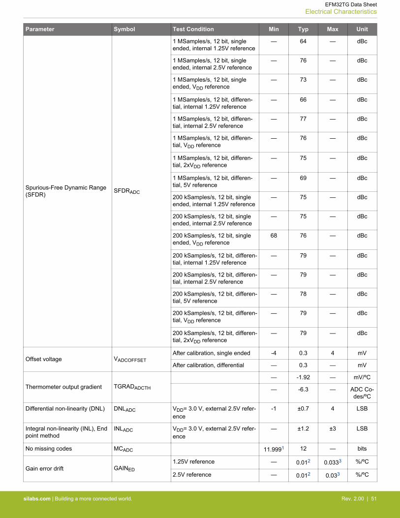
Parameter Symbol Test Condition Min Typ Max Unit
Spurious-Free Dynamic Range(SFDR)
SFDRADC
1 MSamples/s, 12 bit, singleended, internal 1.25V reference
— 64 — dBc
1 MSamples/s, 12 bit, singleended, internal 2.5V reference
— 76 — dBc
1 MSamples/s, 12 bit, singleended, VDD reference
— 73 — dBc
1 MSamples/s, 12 bit, differen-tial, internal 1.25V reference
— 66 — dBc
1 MSamples/s, 12 bit, differen-tial, internal 2.5V reference
— 77 — dBc
1 MSamples/s, 12 bit, differen-tial, VDD reference
— 76 — dBc
1 MSamples/s, 12 bit, differen-tial, 2xVDD reference
— 75 — dBc
1 MSamples/s, 12 bit, differen-tial, 5V reference
— 69 — dBc
200 kSamples/s, 12 bit, singleended, internal 1.25V reference
— 75 — dBc
200 kSamples/s, 12 bit, singleended, internal 2.5V reference
— 75 — dBc
200 kSamples/s, 12 bit, singleended, VDD reference
68 76 — dBc
200 kSamples/s, 12 bit, differen-tial, internal 1.25V reference
— 79 — dBc
200 kSamples/s, 12 bit, differen-tial, internal 2.5V reference
— 79 — dBc
200 kSamples/s, 12 bit, differen-tial, 5V reference
— 78 — dBc
200 kSamples/s, 12 bit, differen-tial, VDD reference
— 79 — dBc
200 kSamples/s, 12 bit, differen-tial, 2xVDD reference
— 79 — dBc
Offset voltage VADCOFFSETAfter calibration, single ended -4 0.3 4 mV
After calibration, differential — 0.3 — mV
Thermometer output gradient TGRADADCTH
— -1.92 — mV/ºC
— -6.3 — ADC Co-des/ºC
Differential non-linearity (DNL) DNLADC VDD= 3.0 V, external 2.5V refer-ence
-1 ±0.7 4 LSB
Integral non-linearity (INL), Endpoint method
INLADC VDD= 3.0 V, external 2.5V refer-ence
— ±1.2 ±3 LSB
No missing codes MCADC 11.9991 12 — bits
Gain error drift GAINED1.25V reference — 0.012 0.0333 %/ºC
2.5V reference — 0.012 0.033 %/ºC
EFM32TG Data SheetElectrical Characteristics
silabs.com | Building a more connected world. Rev. 2.00 | 51
Parameter Symbol Test Condition Min Typ Max Unit
Offset error drift OFFSETED1.25V reference — 0.22 0.73 LSB/ºC
2.5V reference — 0.22 0.623 LSB/ºC
Note:1. On the average every ADC will have one missing code, most likely to appear around 2048 ± n*512 where n can be a value in the
set {-3, -2, -1, 1, 2, 3}. There will be no missing code around 2048, and in spite of the missing code the ADC will be monotonic atall times so that a response to a slowly increasing input will always be a slowly increasing output. Around the one code that ismissing, the neighbour codes will look wider in the DNL plot. The spectra will show spurs on the level of -78dBc for a full scaleinput for chips that have the missing code issue.
2. Typical numbers given by abs(Mean) / (85 - 25).3. Max number given by (abs(Mean) + 3x stddev) / (85 - 25).
The integral non-linearity (INL) and differential non-linearity parameters are explained in the following two figures.
Ideal transfer curve
Digital output code
Analog Input
INL=|[(VD-VSS)/VLSBIDEAL] - D| where 0 < D < 2N- 1
0
1
2
3
4092
4093
4094
4095
VOFFSET
Actual ADC tranfer function before offset and gain correction Actual ADC
tranfer function after offset and gain correction
INL Error (End Point INL)
Figure 4.17. Integral Non-Linearity (INL)
EFM32TG Data SheetElectrical Characteristics
silabs.com | Building a more connected world. Rev. 2.00 | 52
Ideal transfer curve
Digital outputcode
Analog Input
DNL=|[(VD+1 - VD)/VLSBIDEAL] - 1| where 0 < D < 2N- 2
0
1
2
3
4092
4093
4094
4095
Actual transfer function with one missing code.
4
5
Full Scale Range
0.5 LSB
Ideal Code Center
Ideal 50% Transition Point
Ideal spacing between two adjacent codesVLSBIDEAL=1 LSB
Code width =2 LSBDNL=1 LSB
Example: Adjacent input value VD+1
corrresponds to digital output code D+1
Example: Input value VDcorrresponds to digital output code D
Figure 4.18. Differential Non-Linearity (DNL)
EFM32TG Data SheetElectrical Characteristics
silabs.com | Building a more connected world. Rev. 2.00 | 53
4.10.1 Typical Performance
1.25V Reference 2.5V Reference
2XVDDVSS Reference 5VDIFF Reference
VDD Reference
Figure 4.19. ADC Frequency Spectrum, VDD = 3 V, Temp = 25 °C
EFM32TG Data SheetElectrical Characteristics
silabs.com | Building a more connected world. Rev. 2.00 | 54
1.25V Reference 2.5V Reference
2XVDDVSS Reference 5VDIFF Reference
VDD Reference
Figure 4.20. ADC Integral Linearity Error vs Code, VDD = 3 V, Temp = 25 °C
EFM32TG Data SheetElectrical Characteristics
silabs.com | Building a more connected world. Rev. 2.00 | 55
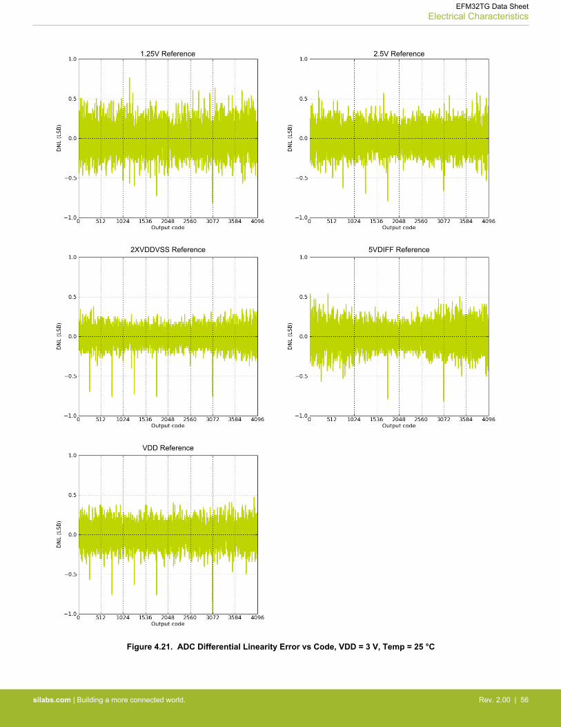
1.25V Reference 2.5V Reference
2XVDDVSS Reference 5VDIFF Reference
VDD Reference
Figure 4.21. ADC Differential Linearity Error vs Code, VDD = 3 V, Temp = 25 °C
EFM32TG Data SheetElectrical Characteristics
silabs.com | Building a more connected world. Rev. 2.00 | 56
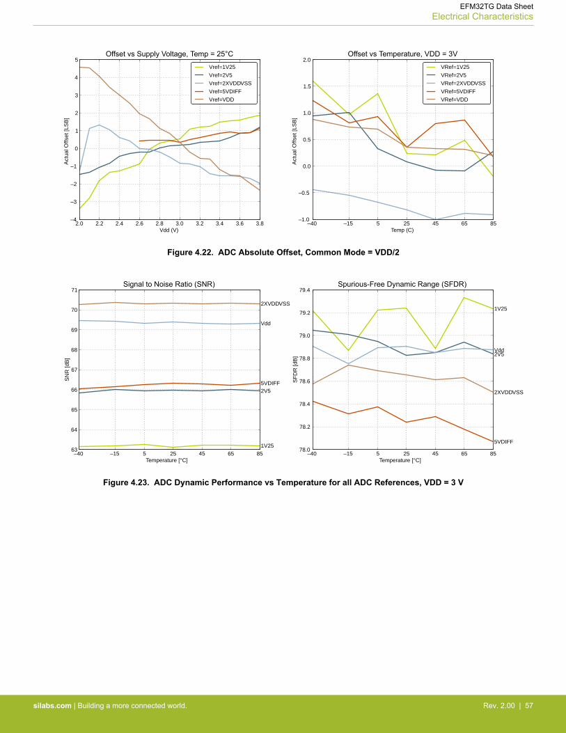
2.0 2.2 2.4 2.6 2.8 3.0 3.2 3.4 3.6 3.8Vdd (V)
–4
–3
–2
–1
0
1
2
3
4
5A
ctua
l Offs
et [L
SB
]Vref=1V25
Vref=2V5
Vref=2XVDDVSS
Vref=5VDIFF
Vref=VDD
–40 –15 5 25 45 65 85Temp (C)
–1.0
–0.5
0.0
0.5
1.0
1.5
2.0
Act
ual O
ffset
[LS
B]
VRef=1V25
VRef=2V5
VRef=2XVDDVSS
VRef=5VDIFF
VRef=VDD
Offset vs Supply Voltage, Temp = 25°C Offset vs Temperature, VDD = 3V
Figure 4.22. ADC Absolute Offset, Common Mode = VDD/2
–40 –15 5 25 45 65 85Temperature [°C]
78.0
78.2
78.4
78.6
78.8
79.0
79.2
79.4S
FD
R [d
B]
1V25
2V5Vdd
5VDIFF
2XVDDVSS
–40 –15 5 25 45 65 85Temperature [°C]
63
64
65
66
67
68
69
70
71
SN
R [d
B]
1V25
2V5
Vdd
5VDIFF
2XVDDVSS
Signal to Noise Ratio (SNR) Spurious-Free Dynamic Range (SFDR)
Figure 4.23. ADC Dynamic Performance vs Temperature for all ADC References, VDD = 3 V
EFM32TG Data SheetElectrical Characteristics
silabs.com | Building a more connected world. Rev. 2.00 | 57
4.11 Digital Analog Converter (DAC)
Table 4.15. DAC
Parameter Symbol Test Condition Min Typ Max Unit
Output voltage range VDACOUT VDD voltage reference, single ended 0 — VDD V
VDD voltage reference, differential -VDD — VDD V
Output common mode voltagerange
VDACCM 0 — VDD V
Active current including referen-ces for 2 channels
IDAC
500 kSamples/s, 12bit — 400 650 µA
100 kSamples/s, 12 bit — 200 250 µA
1 kSamples/s 12 bit NORMAL — 17 25 µA
Sample rate SRDAC — — 500 ksamples/s
DAC clock frequency fDAC
Continuous Mode — — 1000 kHz
Sample/Hold Mode — — 250 kHz
Sample/Off Mode — — 250 kHz
Clock cycles per conversion CYCDAC-
CONV
— 2 — cycles
Conversion time tDACCONV 2 — — µs
Settling time tDACSET-
TLE
— 5 — µs
Signal to Noise Ratio (SNR) SNRDAC
500 kSamples/s, 12 bit, single ended,internal 1.25V reference
— 58 — dB
500 kSamples/s, 12 bit, single ended,internal 2.5V reference
— 59 — dB
500 kSamples/s, 12 bit, differential, in-ternal 1.25V reference
— 58 — dB
500 kSamples/s, 12 bit, differential, in-ternal 2.5V reference
— 58 — dB
500 kSamples/s, 12 bit, differential,VDD reference
— 59 — dB
Signal to Noise-pulse DistortionRatio (SNDR)
SNDRDAC
500 kSamples/s, 12 bit, single ended,internal 1.25V reference
— 57 — dB
500 kSamples/s, 12 bit, single ended,internal 2.5V reference
— 54 — dB
500 kSamples/s, 12 bit, differential, in-ternal 1.25V reference
— 56 — dB
500 kSamples/s, 12 bit, differential, in-ternal 2.5V reference
— 53 — dB
500 kSamples/s, 12 bit, differential,VDD reference
— 55 — dB
EFM32TG Data SheetElectrical Characteristics
silabs.com | Building a more connected world. Rev. 2.00 | 58
Parameter Symbol Test Condition Min Typ Max Unit
Spurious-Free DynamicRange(SFDR)
SFDRDAC
500 kSamples/s, 12 bit, single ended,internal 1.25V reference
— 62 — dBc
500 kSamples/s, 12 bit, single ended,internal 2.5V reference
— 56 — dBc
500 kSamples/s, 12 bit, differential, in-ternal 1.25V reference
— 61 — dBc
500 kSamples/s, 12 bit, differential, in-ternal 2.5V reference
— 55 — dBc
500 kSamples/s, 12 bit, differential,VDD reference
— 60 — dBc
Offset voltage VDACOFF-
SET
After calibration, single ended — 2 — mV
After calibration, differential — 2 — mV
Differential non-linearity DNLDAC VDD= 3.0 V, VDD reference — ±1 — LSB
Integral non-linearity INLDAC VDD= 3.0 V, VDD reference — ±5 — LSB
No missing codes MCDAC — 12 — bits
EFM32TG Data SheetElectrical Characteristics
silabs.com | Building a more connected world. Rev. 2.00 | 59
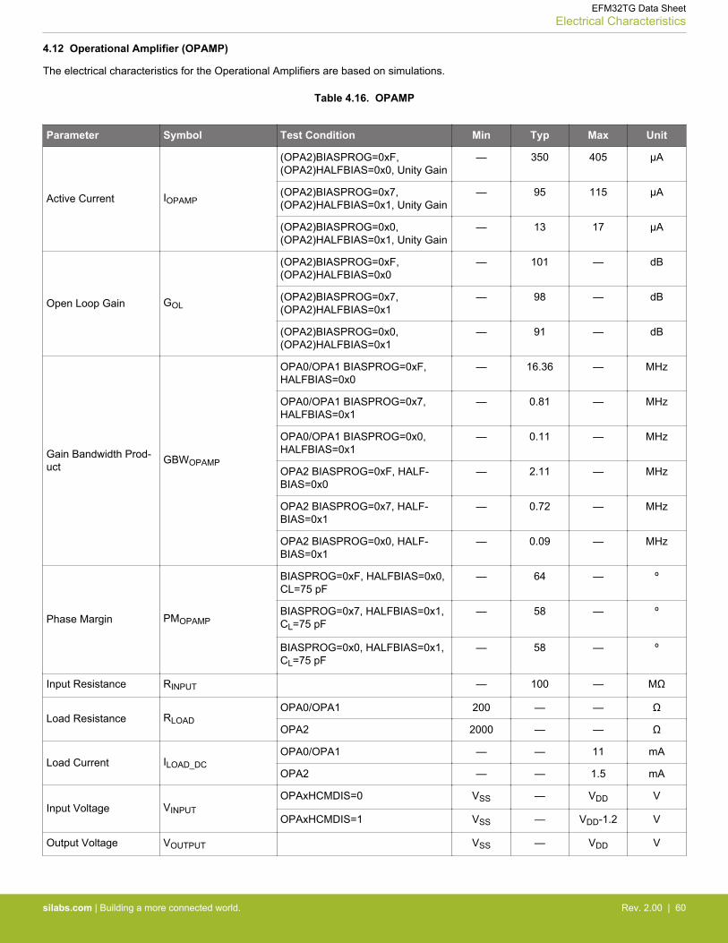
4.12 Operational Amplifier (OPAMP)
The electrical characteristics for the Operational Amplifiers are based on simulations.
Table 4.16. OPAMP
Parameter Symbol Test Condition Min Typ Max Unit
Active Current IOPAMP
(OPA2)BIASPROG=0xF,(OPA2)HALFBIAS=0x0, Unity Gain
— 350 405 µA
(OPA2)BIASPROG=0x7,(OPA2)HALFBIAS=0x1, Unity Gain
— 95 115 µA
(OPA2)BIASPROG=0x0,(OPA2)HALFBIAS=0x1, Unity Gain
— 13 17 µA
Open Loop Gain GOL
(OPA2)BIASPROG=0xF,(OPA2)HALFBIAS=0x0
— 101 — dB
(OPA2)BIASPROG=0x7,(OPA2)HALFBIAS=0x1
— 98 — dB
(OPA2)BIASPROG=0x0,(OPA2)HALFBIAS=0x1
— 91 — dB
Gain Bandwidth Prod-uct
GBWOPAMP
OPA0/OPA1 BIASPROG=0xF,HALFBIAS=0x0
— 16.36 — MHz
OPA0/OPA1 BIASPROG=0x7,HALFBIAS=0x1
— 0.81 — MHz
OPA0/OPA1 BIASPROG=0x0,HALFBIAS=0x1
— 0.11 — MHz
OPA2 BIASPROG=0xF, HALF-BIAS=0x0
— 2.11 — MHz
OPA2 BIASPROG=0x7, HALF-BIAS=0x1
— 0.72 — MHz
OPA2 BIASPROG=0x0, HALF-BIAS=0x1
— 0.09 — MHz
Phase Margin PMOPAMP
BIASPROG=0xF, HALFBIAS=0x0,CL=75 pF
— 64 — º
BIASPROG=0x7, HALFBIAS=0x1,CL=75 pF
— 58 — º
BIASPROG=0x0, HALFBIAS=0x1,CL=75 pF
— 58 — º
Input Resistance RINPUT — 100 — MΩ
Load Resistance RLOADOPA0/OPA1 200 — — Ω
OPA2 2000 — — Ω
Load Current ILOAD_DCOPA0/OPA1 — — 11 mA
OPA2 — — 1.5 mA
Input Voltage VINPUTOPAxHCMDIS=0 VSS — VDD V
OPAxHCMDIS=1 VSS — VDD-1.2 V
Output Voltage VOUTPUT VSS — VDD V
EFM32TG Data SheetElectrical Characteristics
silabs.com | Building a more connected world. Rev. 2.00 | 60
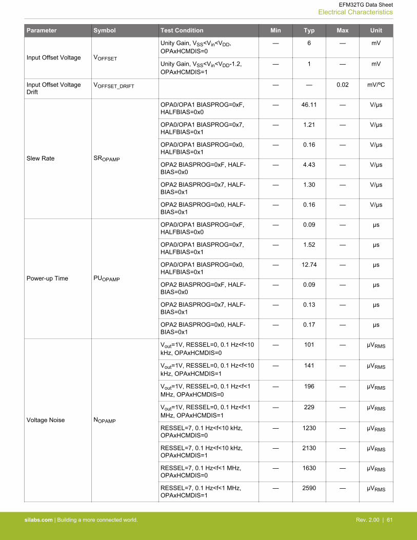
Parameter Symbol Test Condition Min Typ Max Unit
Input Offset Voltage VOFFSET
Unity Gain, VSS<Vin<VDD,OPAxHCMDIS=0
— 6 — mV
Unity Gain, VSS<Vin<VDD-1.2,OPAxHCMDIS=1
— 1 — mV
Input Offset VoltageDrift
VOFFSET_DRIFT — — 0.02 mV/ºC
Slew Rate SROPAMP
OPA0/OPA1 BIASPROG=0xF,HALFBIAS=0x0
— 46.11 — V/µs
OPA0/OPA1 BIASPROG=0x7,HALFBIAS=0x1
— 1.21 — V/µs
OPA0/OPA1 BIASPROG=0x0,HALFBIAS=0x1
— 0.16 — V/µs
OPA2 BIASPROG=0xF, HALF-BIAS=0x0
— 4.43 — V/µs
OPA2 BIASPROG=0x7, HALF-BIAS=0x1
— 1.30 — V/µs
OPA2 BIASPROG=0x0, HALF-BIAS=0x1
— 0.16 — V/µs
Power-up Time PUOPAMP
OPA0/OPA1 BIASPROG=0xF,HALFBIAS=0x0
— 0.09 — µs
OPA0/OPA1 BIASPROG=0x7,HALFBIAS=0x1
— 1.52 — µs
OPA0/OPA1 BIASPROG=0x0,HALFBIAS=0x1
— 12.74 — µs
OPA2 BIASPROG=0xF, HALF-BIAS=0x0
— 0.09 — µs
OPA2 BIASPROG=0x7, HALF-BIAS=0x1
— 0.13 — µs
OPA2 BIASPROG=0x0, HALF-BIAS=0x1
— 0.17 — µs
Voltage Noise NOPAMP
Vout=1V, RESSEL=0, 0.1 Hz<f<10kHz, OPAxHCMDIS=0
— 101 — µVRMS
Vout=1V, RESSEL=0, 0.1 Hz<f<10kHz, OPAxHCMDIS=1
— 141 — µVRMS
Vout=1V, RESSEL=0, 0.1 Hz<f<1MHz, OPAxHCMDIS=0
— 196 — µVRMS
Vout=1V, RESSEL=0, 0.1 Hz<f<1MHz, OPAxHCMDIS=1
— 229 — µVRMS
RESSEL=7, 0.1 Hz<f<10 kHz,OPAxHCMDIS=0
— 1230 — µVRMS
RESSEL=7, 0.1 Hz<f<10 kHz,OPAxHCMDIS=1
— 2130 — µVRMS
RESSEL=7, 0.1 Hz<f<1 MHz,OPAxHCMDIS=0
— 1630 — µVRMS
RESSEL=7, 0.1 Hz<f<1 MHz,OPAxHCMDIS=1
— 2590 — µVRMS
EFM32TG Data SheetElectrical Characteristics
silabs.com | Building a more connected world. Rev. 2.00 | 61
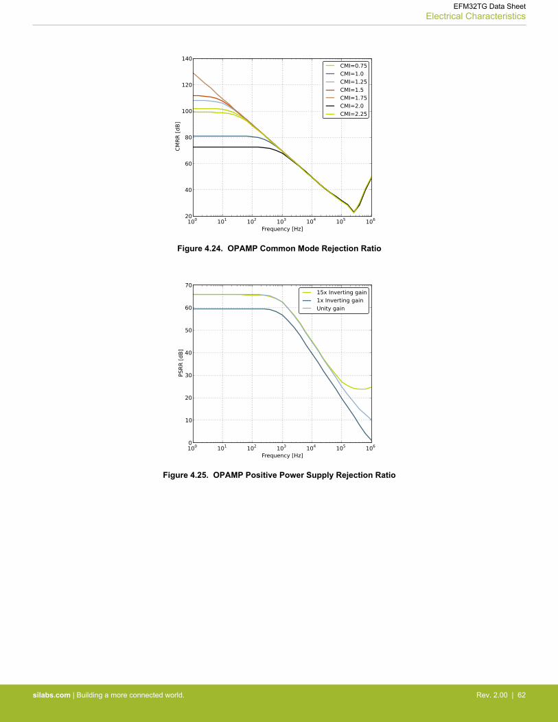
Figure 4.24. OPAMP Common Mode Rejection Ratio
Figure 4.25. OPAMP Positive Power Supply Rejection Ratio
EFM32TG Data SheetElectrical Characteristics
silabs.com | Building a more connected world. Rev. 2.00 | 62
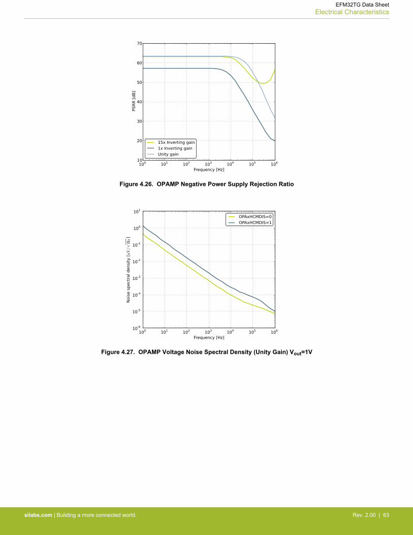
Figure 4.26. OPAMP Negative Power Supply Rejection Ratio
Figure 4.27. OPAMP Voltage Noise Spectral Density (Unity Gain) Vout=1V
EFM32TG Data SheetElectrical Characteristics
silabs.com | Building a more connected world. Rev. 2.00 | 63
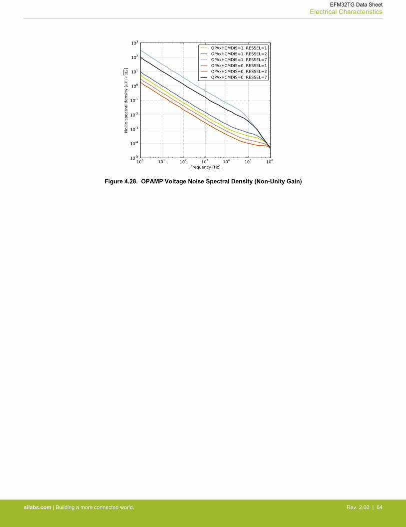
Figure 4.28. OPAMP Voltage Noise Spectral Density (Non-Unity Gain)
EFM32TG Data SheetElectrical Characteristics
silabs.com | Building a more connected world. Rev. 2.00 | 64
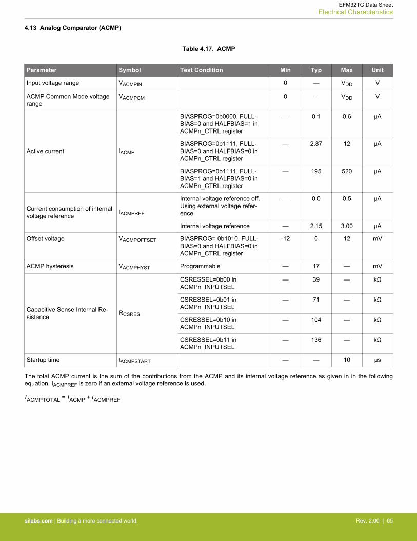
4.13 Analog Comparator (ACMP)
Table 4.17. ACMP
Parameter Symbol Test Condition Min Typ Max Unit
Input voltage range VACMPIN 0 — VDD V
ACMP Common Mode voltagerange
VACMPCM 0 — VDD V
Active current IACMP
BIASPROG=0b0000, FULL-BIAS=0 and HALFBIAS=1 inACMPn_CTRL register
— 0.1 0.6 µA
BIASPROG=0b1111, FULL-BIAS=0 and HALFBIAS=0 inACMPn_CTRL register
— 2.87 12 µA
BIASPROG=0b1111, FULL-BIAS=1 and HALFBIAS=0 inACMPn_CTRL register
— 195 520 µA
Current consumption of internalvoltage reference
IACMPREF
Internal voltage reference off.Using external voltage refer-ence
— 0.0 0.5 µA
Internal voltage reference — 2.15 3.00 µA
Offset voltage VACMPOFFSET BIASPROG= 0b1010, FULL-BIAS=0 and HALFBIAS=0 inACMPn_CTRL register
-12 0 12 mV
ACMP hysteresis VACMPHYST Programmable — 17 — mV
Capacitive Sense Internal Re-sistance
RCSRES
CSRESSEL=0b00 inACMPn_INPUTSEL
— 39 — kΩ
CSRESSEL=0b01 inACMPn_INPUTSEL
— 71 — kΩ
CSRESSEL=0b10 inACMPn_INPUTSEL
— 104 — kΩ
CSRESSEL=0b11 inACMPn_INPUTSEL
— 136 — kΩ
Startup time tACMPSTART — — 10 µs
The total ACMP current is the sum of the contributions from the ACMP and its internal voltage reference as given in in the followingequation. IACMPREF is zero if an external voltage reference is used.
IACMPTOTAL = IACMP + IACMPREF
EFM32TG Data SheetElectrical Characteristics
silabs.com | Building a more connected world. Rev. 2.00 | 65
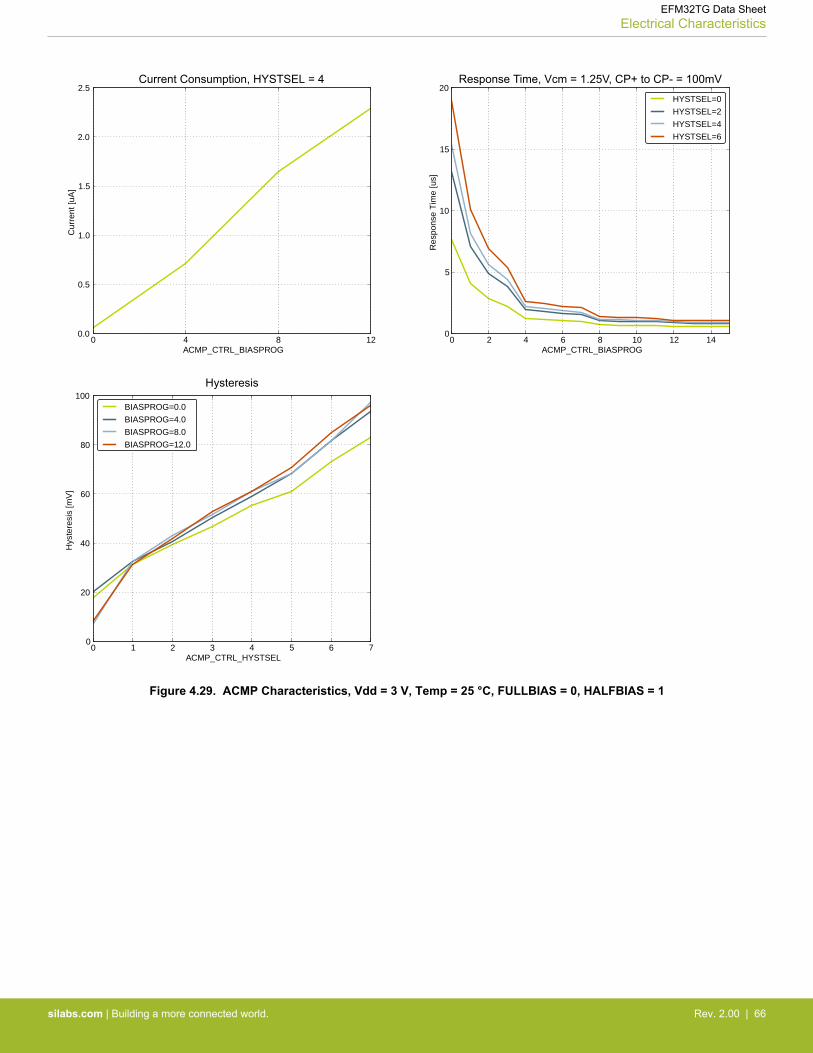
0 2 4 6 8 10 12 14ACMP_CTRL_BIASPROG
0
5
10
15
20
Res
pons
e T
ime
[us]
HYSTSEL=0
HYSTSEL=2
HYSTSEL=4
HYSTSEL=6
0 4 8 12ACMP_CTRL_BIASPROG
0.0
0.5
1.0
1.5
2.0
2.5
Cur
rent
[uA
]
0 1 2 3 4 5 6 7ACMP_CTRL_HYSTSEL
0
20
40
60
80
100
Hys
tere
sis
[mV
]
BIASPROG=0.0
BIASPROG=4.0
BIASPROG=8.0
BIASPROG=12.0
Current Consumption, HYSTSEL = 4 Response Time, Vcm = 1.25V, CP+ to CP- = 100mV
Hysteresis
Figure 4.29. ACMP Characteristics, Vdd = 3 V, Temp = 25 °C, FULLBIAS = 0, HALFBIAS = 1
EFM32TG Data SheetElectrical Characteristics
silabs.com | Building a more connected world. Rev. 2.00 | 66
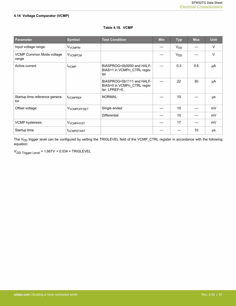
4.14 Voltage Comparator (VCMP)
Table 4.18. VCMP
Parameter Symbol Test Condition Min Typ Max Unit
Input voltage range VVCMPIN — VDD — V
VCMP Common Mode voltagerange
VVCMPCM — VDD — V
Active current IVCMP BIASPROG=0b0000 and HALF-BIAS=1 in VCMPn_CTRL regis-ter
— 0.3 0.6 µA
BIASPROG=0b1111 and HALF-BIAS=0 in VCMPn_CTRL regis-ter. LPREF=0.
— 22 30 µA
Startup time reference genera-tor
tVCMPREF NORMAL — 10 — µs
Offset voltage VVCMPOFFSET Single ended — 10 — mV
Differential — 10 — mV
VCMP hysteresis VVCMPHYST — 17 — mV
Startup time tVCMPSTART — — 10 µs
The VDD trigger level can be configured by setting the TRIGLEVEL field of the VCMP_CTRL register in accordance with the followingequation:
VDD Trigger Level = 1.667V + 0.034 × TRIGLEVEL
EFM32TG Data SheetElectrical Characteristics
silabs.com | Building a more connected world. Rev. 2.00 | 67
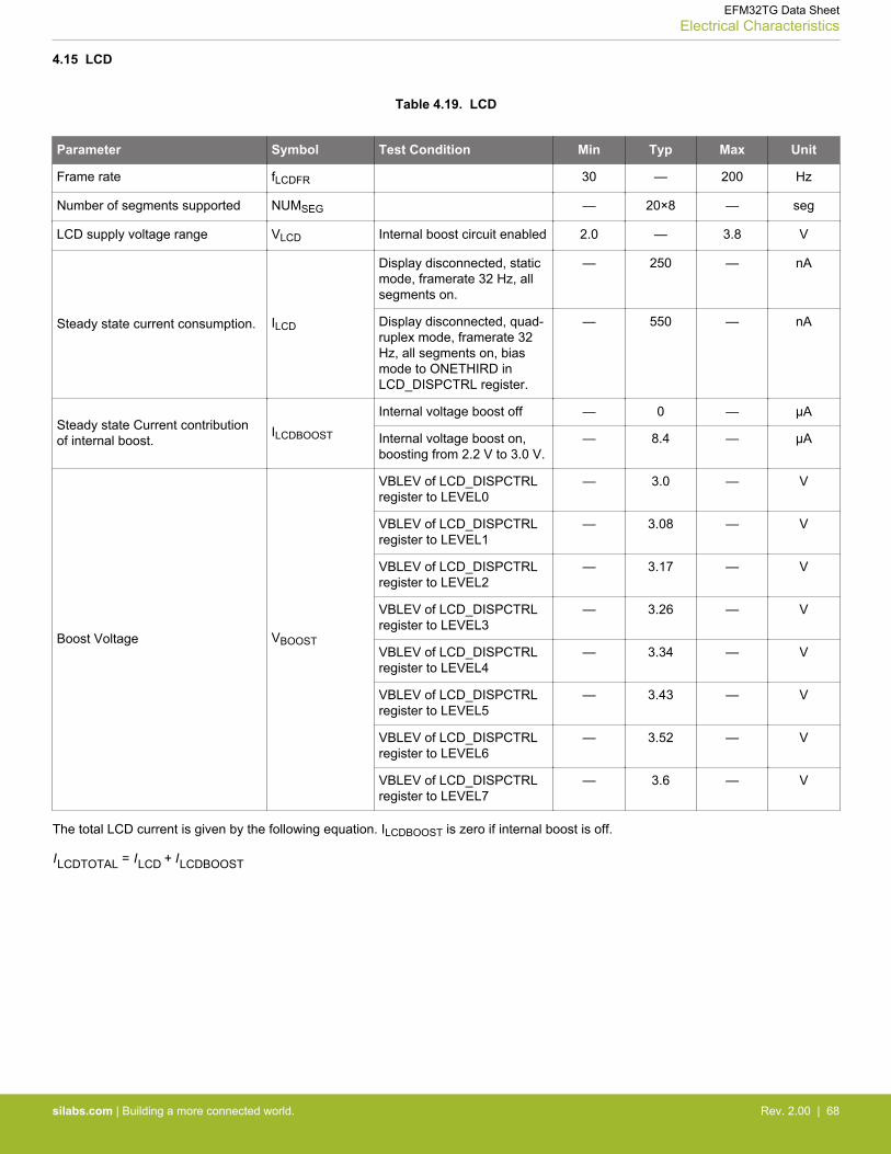
4.15 LCD
Table 4.19. LCD
Parameter Symbol Test Condition Min Typ Max Unit
Frame rate fLCDFR 30 — 200 Hz
Number of segments supported NUMSEG — 20×8 — seg
LCD supply voltage range VLCD Internal boost circuit enabled 2.0 — 3.8 V
Steady state current consumption. ILCD
Display disconnected, staticmode, framerate 32 Hz, allsegments on.
— 250 — nA
Display disconnected, quad-ruplex mode, framerate 32Hz, all segments on, biasmode to ONETHIRD inLCD_DISPCTRL register.
— 550 — nA
Steady state Current contributionof internal boost.
ILCDBOOST
Internal voltage boost off — 0 — µA
Internal voltage boost on,boosting from 2.2 V to 3.0 V.
— 8.4 — µA
Boost Voltage VBOOST
VBLEV of LCD_DISPCTRLregister to LEVEL0
— 3.0 — V
VBLEV of LCD_DISPCTRLregister to LEVEL1
— 3.08 — V
VBLEV of LCD_DISPCTRLregister to LEVEL2
— 3.17 — V
VBLEV of LCD_DISPCTRLregister to LEVEL3
— 3.26 — V
VBLEV of LCD_DISPCTRLregister to LEVEL4
— 3.34 — V
VBLEV of LCD_DISPCTRLregister to LEVEL5
— 3.43 — V
VBLEV of LCD_DISPCTRLregister to LEVEL6
— 3.52 — V
VBLEV of LCD_DISPCTRLregister to LEVEL7
— 3.6 — V
The total LCD current is given by the following equation. ILCDBOOST is zero if internal boost is off.
ILCDTOTAL = ILCD + ILCDBOOST
EFM32TG Data SheetElectrical Characteristics
silabs.com | Building a more connected world. Rev. 2.00 | 68
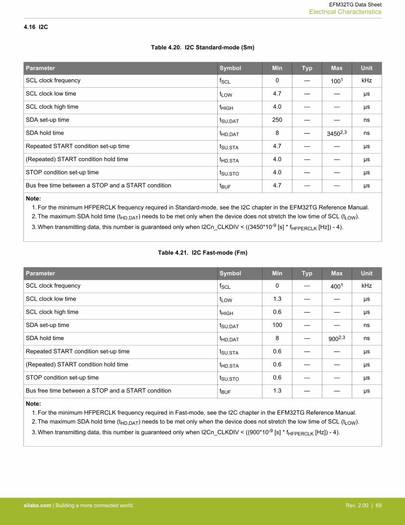
4.16 I2C
Table 4.20. I2C Standard-mode (Sm)
Parameter Symbol Min Typ Max Unit
SCL clock frequency fSCL 0 — 1001 kHz
SCL clock low time tLOW 4.7 — — µs
SCL clock high time tHIGH 4.0 — — µs
SDA set-up time tSU,DAT 250 — — ns
SDA hold time tHD,DAT 8 — 34502,3 ns
Repeated START condition set-up time tSU,STA 4.7 — — µs
(Repeated) START condition hold time tHD,STA 4.0 — — µs
STOP condition set-up time tSU,STO 4.0 — — µs
Bus free time between a STOP and a START condition tBUF 4.7 — — µs
Note:1. For the minimum HFPERCLK frequency required in Standard-mode, see the I2C chapter in the EFM32TG Reference Manual.2. The maximum SDA hold time (tHD,DAT) needs to be met only when the device does not stretch the low time of SCL (tLOW).
3. When transmitting data, this number is guaranteed only when I2Cn_CLKDIV < ((3450*10-9 [s] * fHFPERCLK [Hz]) - 4).
Table 4.21. I2C Fast-mode (Fm)
Parameter Symbol Min Typ Max Unit
SCL clock frequency fSCL 0 — 4001 kHz
SCL clock low time tLOW 1.3 — — µs
SCL clock high time tHIGH 0.6 — — µs
SDA set-up time tSU,DAT 100 — — ns
SDA hold time tHD,DAT 8 — 9002,3 ns
Repeated START condition set-up time tSU,STA 0.6 — — µs
(Repeated) START condition hold time tHD,STA 0.6 — — µs
STOP condition set-up time tSU,STO 0.6 — — µs
Bus free time between a STOP and a START condition tBUF 1.3 — — µs
Note:1. For the minimum HFPERCLK frequency required in Fast-mode, see the I2C chapter in the EFM32TG Reference Manual.2. The maximum SDA hold time (tHD,DAT) needs to be met only when the device does not stretch the low time of SCL (tLOW).
3. When transmitting data, this number is guaranteed only when I2Cn_CLKDIV < ((900*10-9 [s] * fHFPERCLK [Hz]) - 4).
EFM32TG Data SheetElectrical Characteristics
silabs.com | Building a more connected world. Rev. 2.00 | 69
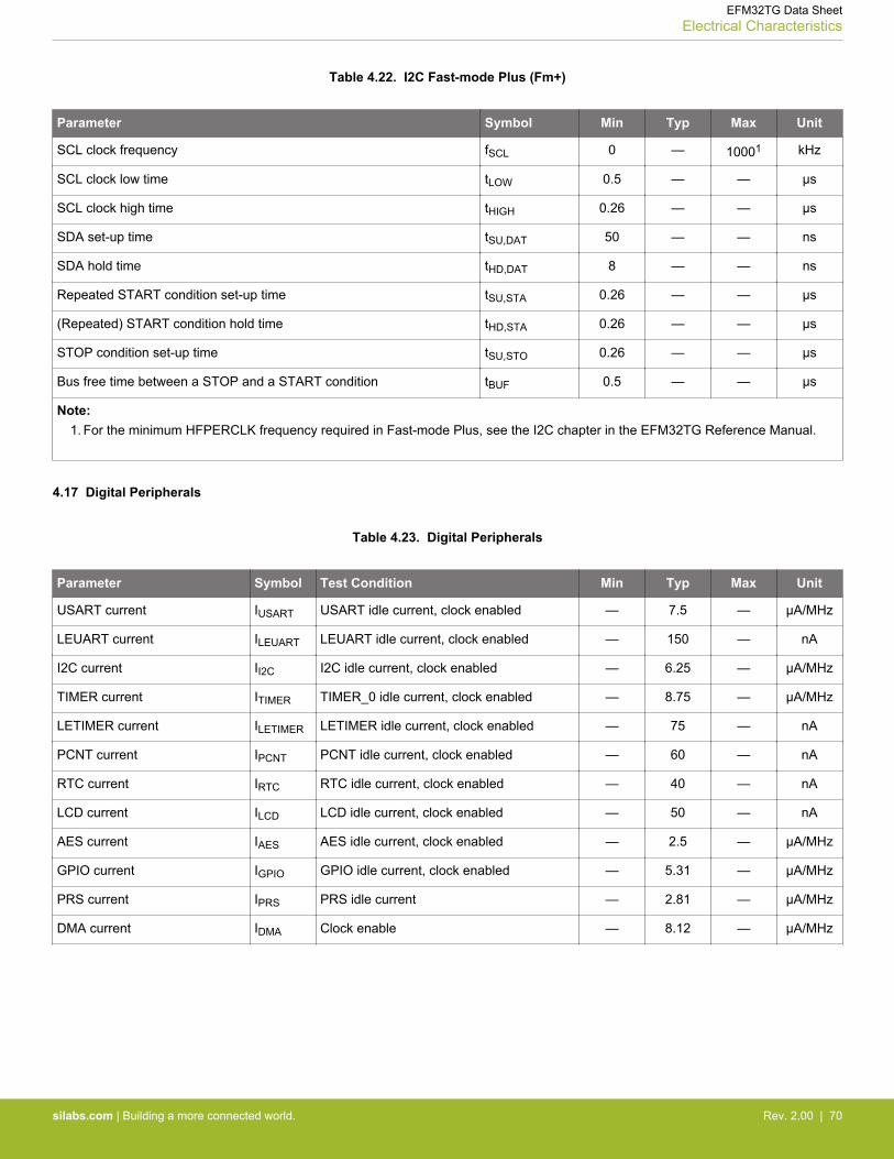
Table 4.22. I2C Fast-mode Plus (Fm+)
Parameter Symbol Min Typ Max Unit
SCL clock frequency fSCL 0 — 10001 kHz
SCL clock low time tLOW 0.5 — — µs
SCL clock high time tHIGH 0.26 — — µs
SDA set-up time tSU,DAT 50 — — ns
SDA hold time tHD,DAT 8 — — ns
Repeated START condition set-up time tSU,STA 0.26 — — µs
(Repeated) START condition hold time tHD,STA 0.26 — — µs
STOP condition set-up time tSU,STO 0.26 — — µs
Bus free time between a STOP and a START condition tBUF 0.5 — — µs
Note:1. For the minimum HFPERCLK frequency required in Fast-mode Plus, see the I2C chapter in the EFM32TG Reference Manual.
4.17 Digital Peripherals
Table 4.23. Digital Peripherals
Parameter Symbol Test Condition Min Typ Max Unit
USART current IUSART USART idle current, clock enabled — 7.5 — µA/MHz
LEUART current ILEUART LEUART idle current, clock enabled — 150 — nA
I2C current II2C I2C idle current, clock enabled — 6.25 — µA/MHz
TIMER current ITIMER TIMER_0 idle current, clock enabled — 8.75 — µA/MHz
LETIMER current ILETIMER LETIMER idle current, clock enabled — 75 — nA
PCNT current IPCNT PCNT idle current, clock enabled — 60 — nA
RTC current IRTC RTC idle current, clock enabled — 40 — nA
LCD current ILCD LCD idle current, clock enabled — 50 — nA
AES current IAES AES idle current, clock enabled — 2.5 — µA/MHz
GPIO current IGPIO GPIO idle current, clock enabled — 5.31 — µA/MHz
PRS current IPRS PRS idle current — 2.81 — µA/MHz
DMA current IDMA Clock enable — 8.12 — µA/MHz
EFM32TG Data SheetElectrical Characteristics
silabs.com | Building a more connected world. Rev. 2.00 | 70

5. Pin Definitions
Note: Please refer to the application note AN0002 EFM32 Hardware Design Considerations for guidelines on designing Printed CircuitBoards (PCBs) for the EFM32TG.
EFM32TG Data SheetPin Definitions
silabs.com | Building a more connected world. Rev. 2.00 | 71
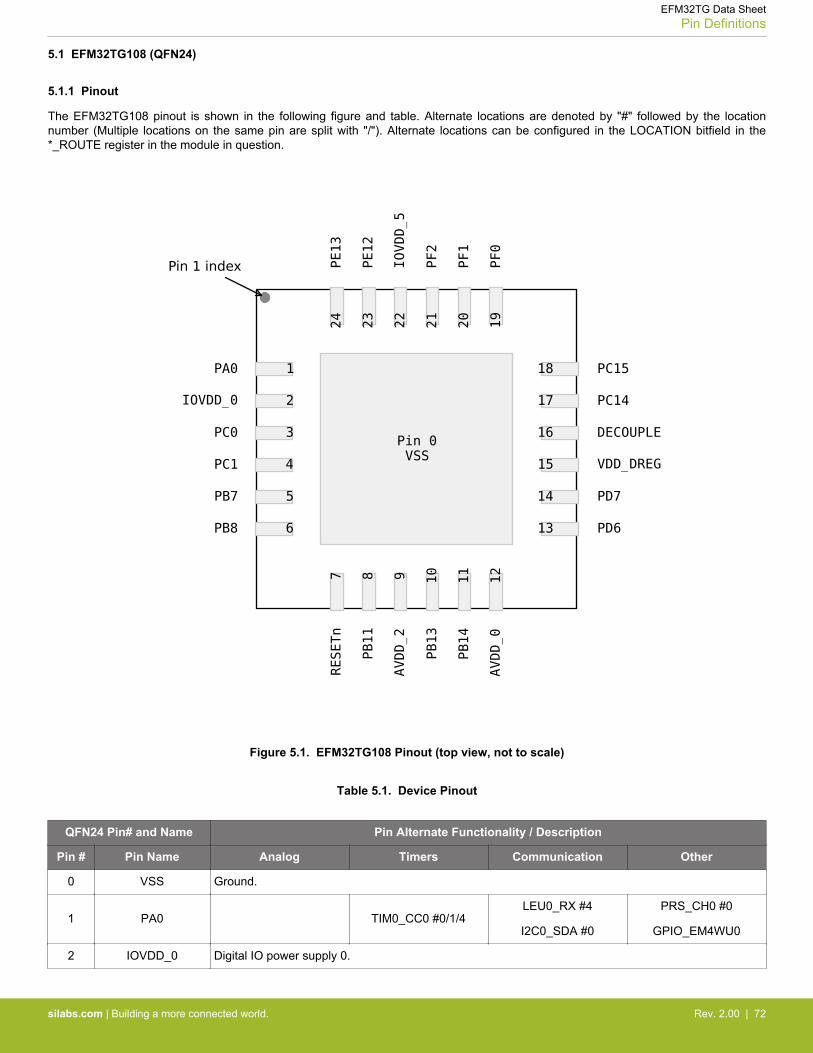
5.1 EFM32TG108 (QFN24)
5.1.1 Pinout
The EFM32TG108 pinout is shown in the following figure and table. Alternate locations are denoted by "#" followed by the locationnumber (Multiple locations on the same pin are split with "/"). Alternate locations can be configured in the LOCATION bitfield in the*_ROUTE register in the module in question.
Figure 5.1. EFM32TG108 Pinout (top view, not to scale)
Table 5.1. Device Pinout
QFN24 Pin# and Name Pin Alternate Functionality / Description
Pin # Pin Name Analog Timers Communication Other
0 VSS Ground.
1 PA0 TIM0_CC0 #0/1/4LEU0_RX #4
I2C0_SDA #0
PRS_CH0 #0
GPIO_EM4WU0
2 IOVDD_0 Digital IO power supply 0.
EFM32TG Data SheetPin Definitions
silabs.com | Building a more connected world. Rev. 2.00 | 72
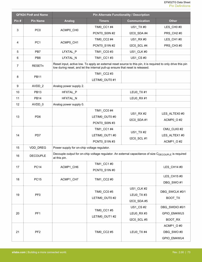
QFN24 Pin# and Name Pin Alternate Functionality / Description
Pin # Pin Name Analog Timers Communication Other
3 PC0 ACMP0_CH0TIM0_CC1 #4
PCNT0_S0IN #2
US1_TX #0
I2C0_SDA #4
LES_CH0 #0
PRS_CH2 #0
4 PC1 ACMP0_CH1TIM0_CC2 #4
PCNT0_S1IN #2
US1_RX #0
I2C0_SCL #4
LES_CH1 #0
PRS_CH3 #0
5 PB7 LFXTAL_P TIM1_CC0 #3 US1_CLK #0
6 PB8 LFXTAL_N TIM1_CC1 #3 US1_CS #0
7 RESETn Reset input, active low. To apply an external reset source to this pin, it is required to only drive this pinlow during reset, and let the internal pull-up ensure that reset is released.
8 PB11TIM1_CC2 #3
LETIM0_OUT0 #1
9 AVDD_2 Analog power supply 2.
10 PB13 HFXTAL_P LEU0_TX #1
11 PB14 HFXTAL_N LEU0_RX #1
12 AVDD_0 Analog power supply 0.
13 PD6
TIM1_CC0 #4
LETIM0_OUT0 #0
PCNT0_S0IN #3
US1_RX #2
I2C0_SDA #1
LES_ALTEX0 #0
ACMP0_O #2
14 PD7
TIM1_CC1 #4
LETIM0_OUT1 #0
PCNT0_S1IN #3
US1_TX #2
I2C0_SCL #1
CMU_CLK0 #2
LES_ALTEX1 #0
ACMP1_O #2
15 VDD_DREG Power supply for on-chip voltage regulator.
16 DECOUPLEDecouple output for on-chip voltage regulator. An external capacitance of size CDECOUPLE is requiredat this pin.
17 PC14 ACMP1_CH6TIM1_CC1 #0
PCNT0_S1IN #0LES_CH14 #0
18 PC15 ACMP1_CH7 TIM1_CC2 #0LES_CH15 #0
DBG_SWO #1
19 PF0TIM0_CC0 #5
LETIM0_OUT0 #2
US1_CLK #2
LEU0_TX #3
I2C0_SDA #5
DBG_SWCLK #0/1
BOOT_TX
20 PF1TIM0_CC1 #5
LETIM0_OUT1 #2
US1_CS #2
LEU0_RX #3
I2C0_SCL #5
DBG_SWDIO #0/1
GPIO_EM4WU3
BOOT_RX
21 PF2 TIM0_CC2 #5 LEU0_TX #4
ACMP1_O #0
DBG_SWO #0
GPIO_EM4WU4
EFM32TG Data SheetPin Definitions
silabs.com | Building a more connected world. Rev. 2.00 | 73
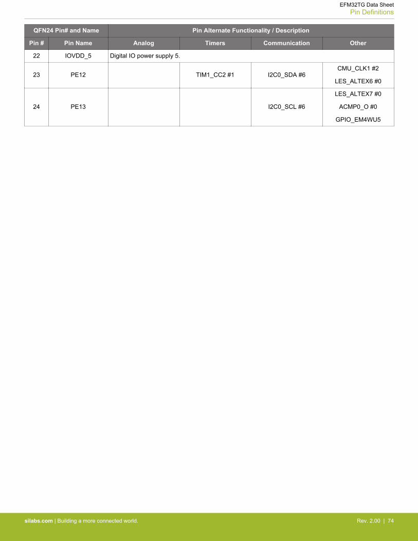
QFN24 Pin# and Name Pin Alternate Functionality / Description
Pin # Pin Name Analog Timers Communication Other
22 IOVDD_5 Digital IO power supply 5.
23 PE12 TIM1_CC2 #1 I2C0_SDA #6CMU_CLK1 #2
LES_ALTEX6 #0
24 PE13 I2C0_SCL #6
LES_ALTEX7 #0
ACMP0_O #0
GPIO_EM4WU5
EFM32TG Data SheetPin Definitions
silabs.com | Building a more connected world. Rev. 2.00 | 74
5.1.2 Alternate Functionality Pinout
A wide selection of alternate functionality is available for multiplexing to various pins. This is shown in the following table. The tableshows the name of the alternate functionality in the first column, followed by columns showing the possible LOCATION bitfield settings.
Note: Some functionality, such as analog interfaces, do not have alternate settings or a LOCATION bitfield. In these cases, the pinoutis shown in the column corresponding to LOCATION 0.
Table 5.2. Alternate functionality overview
Alternate LOCATION
Functionality 0 1 2 3 4 5 6 Description
ACMP0_CH0 PC0 Analog comparator ACMP0, channel 0.
ACMP0_CH1 PC1 Analog comparator ACMP0, channel 1.
ACMP0_O PE13 PD6 Analog comparator ACMP0, digital output.
ACMP1_CH6 PC14 Analog comparator ACMP1, channel 6.
ACMP1_CH7 PC15 Analog comparator ACMP1, channel 7.
ACMP1_O PF2 PD7 Analog comparator ACMP1, digital output.
BOOT_RX PF1 Bootloader RX.
BOOT_TX PF0 Bootloader TX.
CMU_CLK0 PD7 Clock Management Unit, clock output number 0.
CMU_CLK1 PE12 Clock Management Unit, clock output number 1.
DBG_SWCLK PF0 PF0Debug-interface Serial Wire clock input.
Note that this function is enabled to pin out of reset,and has a built-in pull down.
DBG_SWDIO PF1 PF1Debug-interface Serial Wire data input / output.
Note that this function is enabled to pin out of reset,and has a built-in pull up.
DBG_SWO PF2 PC15Debug-interface Serial Wire viewer Output.
Note that this function is not enabled after reset, andmust be enabled by software to be used.
GPIO_EM4WU0 PA0 Pin can be used to wake the system up from EM4
GPIO_EM4WU3 PF1 Pin can be used to wake the system up from EM4
GPIO_EM4WU4 PF2 Pin can be used to wake the system up from EM4
GPIO_EM4WU5 PE13 Pin can be used to wake the system up from EM4
HFXTAL_N PB14 High Frequency Crystal negative pin. Also used asexternal optional clock input pin.
HFXTAL_P PB13 High Frequency Crystal positive pin.
I2C0_SCL PD7 PC1 PF1 PE13 I2C0 Serial Clock Line input / output.
I2C0_SDA PA0 PD6 PC0 PF0 PE12 I2C0 Serial Data input / output.
LES_ALTEX0 PD6 LESENSE alternate exite output 0.
LES_ALTEX1 PD7 LESENSE alternate exite output 1.
LES_ALTEX6 PE12 LESENSE alternate exite output 6.
EFM32TG Data SheetPin Definitions
silabs.com | Building a more connected world. Rev. 2.00 | 75
Alternate LOCATION
Functionality 0 1 2 3 4 5 6 Description
LES_ALTEX7 PE13 LESENSE alternate exite output 7.
LES_CH0 PC0 LESENSE channel 0.
LES_CH1 PC1 LESENSE channel 1.
LES_CH14 PC14 LESENSE channel 14.
LES_CH15 PC15 LESENSE channel 15.
LETIM0_OUT0 PD6 PB11 PF0 Low Energy Timer LETIM0, output channel 0.
LETIM0_OUT1 PD7 PF1 Low Energy Timer LETIM0, output channel 1.
LEU0_RX PB14 PF1 PA0 LEUART0 Receive input.
LEU0_TX PB13 PF0 PF2 LEUART0 Transmit output. Also used as receive in-put in half duplex communication.
LFXTAL_N PB8Low Frequency Crystal (typically 32.768 kHz) nega-tive pin. Also used as an optional external clock in-put pin.
LFXTAL_P PB7 Low Frequency Crystal (typically 32.768 kHz) posi-tive pin.
PCNT0_S0IN PC0 PD6 Pulse Counter PCNT0 input number 0.
PCNT0_S1IN PC14 PC1 PD7 Pulse Counter PCNT0 input number 1.
PRS_CH0 PA0 Peripheral Reflex System PRS, channel 0.
PRS_CH2 PC0 Peripheral Reflex System PRS, channel 2.
PRS_CH3 PC1 Peripheral Reflex System PRS, channel 3.
TIM0_CC0 PA0 PA0 PA0 PF0 Timer 0 Capture Compare input / output channel 0.
TIM0_CC1 PC0 PF1 Timer 0 Capture Compare input / output channel 1.
TIM0_CC2 PC1 PF2 Timer 0 Capture Compare input / output channel 2.
TIM1_CC0 PB7 PD6 Timer 1 Capture Compare input / output channel 0.
TIM1_CC1 PC14 PB8 PD7 Timer 1 Capture Compare input / output channel 1.
TIM1_CC2 PC15 PE12 PB11 Timer 1 Capture Compare input / output channel 2.
US1_CLK PB7 PF0 USART1 clock input / output.
US1_CS PB8 PF1 USART1 chip select input / output.
US1_RX PC1 PD6USART1 Asynchronous Receive.
USART1 Synchronous mode Master Input / SlaveOutput (MISO).
US1_TX PC0 PD7
USART1 Asynchronous Transmit.Also used as re-ceive input in half duplex communication.
USART1 Synchronous mode Master Output / SlaveInput (MOSI).
EFM32TG Data SheetPin Definitions
silabs.com | Building a more connected world. Rev. 2.00 | 76
5.1.3 GPIO Pinout Overview
The specific GPIO pins available in EFM32TG108 is shown in the following table. Each GPIO port is organized as 16-bit ports indicatedby letters A through F, and the individual pin on this port is indicated by a number from 15 down to 0.
Table 5.3. GPIO Pinout
Port Pin15
Pin14
Pin13
Pin12
Pin11
Pin10
Pin 9 Pin 8 Pin 7 Pin 6 Pin 5 Pin 4 Pin 3 Pin 2 Pin 1 Pin 0
Port A - - - - - - - - - - - - - - - PA0
Port B - PB14 PB13 - PB11 - - PB8 PB7 - - - - - - -
Port C PC15 PC14 - - - - - - - - - - - - PC1 PC0
Port D - - - - - - - - PD7 PD6 - - - - - -
Port E - - PE13 PE12 - - - - - - - - - - - -
Port F - - - - - - - - - - - - - PF2 PF1 PF0
EFM32TG Data SheetPin Definitions
silabs.com | Building a more connected world. Rev. 2.00 | 77

5.2 EFM32TG110 (QFN24)
5.2.1 Pinout
The EFM32TG110 pinout is shown in the following figure and table. Alternate locations are denoted by "#" followed by the locationnumber (Multiple locations on the same pin are split with "/"). Alternate locations can be configured in the LOCATION bitfield in the*_ROUTE register in the module in question.
Figure 5.2. EFM32TG110 Pinout (top view, not to scale)
Table 5.4. Device Pinout
QFN24 Pin# and Name Pin Alternate Functionality / Description
Pin # Pin Name Analog Timers Communication Other
0 VSS Ground.
1 PA0 TIM0_CC0 #0/1/4LEU0_RX #4
I2C0_SDA #0
PRS_CH0 #0
GPIO_EM4WU0
2 IOVDD_0 Digital IO power supply 0.
EFM32TG Data SheetPin Definitions
silabs.com | Building a more connected world. Rev. 2.00 | 78
QFN24 Pin# and Name Pin Alternate Functionality / Description
Pin # Pin Name Analog Timers Communication Other
3 PC0
ACMP0_CH0
DAC0_OUT0ALT #0/
OPAMP_OUT0ALT
TIM0_CC1 #4
PCNT0_S0IN #2
US0_TX #5
US1_TX #0
I2C0_SDA #4
LES_CH0 #0
PRS_CH2 #0
4 PC1
ACMP0_CH1
DAC0_OUT0ALT #1/
OPAMP_OUT0ALT
TIM0_CC2 #4
PCNT0_S1IN #2
US0_RX #5
US1_RX #0
I2C0_SCL #4
LES_CH1 #0
PRS_CH3 #0
5 PB7 LFXTAL_P TIM1_CC0 #3US0_TX #4
US1_CLK #0
6 PB8 LFXTAL_N TIM1_CC1 #3US0_RX #4
US1_CS #0
7 RESETn Reset input, active low. To apply an external reset source to this pin, it is required to only drive this pinlow during reset, and let the internal pull-up ensure that reset is released.
8 PB11DAC0_OUT0 /
OPAMP_OUT0
TIM1_CC2 #3
LETIM0_OUT0 #1
9 AVDD_2 Analog power supply 2.
10 PB13 HFXTAL_PUS0_CLK #4/5
LEU0_TX #1
11 PB14 HFXTAL_NUS0_CS #4/5
LEU0_RX #1
12 AVDD_0 Analog power supply 0.
13 PD6
ADC0_CH6
DAC0_P1/
OPAMP_P1
TIM1_CC0 #4
LETIM0_OUT0 #0
PCNT0_S0IN #3
US1_RX #2
I2C0_SDA #1
LES_ALTEX0 #0
ACMP0_O #2
14 PD7
ADC0_CH7
DAC0_N1/
OPAMP_N1
TIM1_CC1 #4
LETIM0_OUT1 #0
PCNT0_S1IN #3
US1_TX #2
I2C0_SCL #1
CMU_CLK0 #2
LES_ALTEX1 #0
ACMP1_O #2
15 VDD_DREG Power supply for on-chip voltage regulator.
16 DECOUPLEDecouple output for on-chip voltage regulator. An external capacitance of size CDECOUPLE is requiredat this pin.
17 PC14
ACMP1_CH6
DAC0_OUT1ALT #2/
OPAMP_OUT1ALT
TIM1_CC1 #0
PCNT0_S1IN #0US0_CS #3 LES_CH14 #0
18 PC15
ACMP1_CH7
DAC0_OUT1ALT #3/
OPAMP_OUT1ALT
TIM1_CC2 #0 US0_CLK #3LES_CH15 #0
DBG_SWO #1
EFM32TG Data SheetPin Definitions
silabs.com | Building a more connected world. Rev. 2.00 | 79
QFN24 Pin# and Name Pin Alternate Functionality / Description
Pin # Pin Name Analog Timers Communication Other
19 PF0TIM0_CC0 #5
LETIM0_OUT0 #2
US1_CLK #2
LEU0_TX #3
I2C0_SDA #5
DBG_SWCLK #0/1
BOOT_TX
20 PF1TIM0_CC1 #5
LETIM0_OUT1 #2
US1_CS #2
LEU0_RX #3
I2C0_SCL #5
DBG_SWDIO #0/1
GPIO_EM4WU3
BOOT_RX
21 PF2 TIM0_CC2 #5 LEU0_TX #4
ACMP1_O #0
DBG_SWO #0
GPIO_EM4WU4
22 IOVDD_5 Digital IO power supply 5.
23 PE12 TIM1_CC2 #1
US0_RX #3
US0_CLK #0
I2C0_SDA #6
CMU_CLK1 #2
LES_ALTEX6 #0
24 PE13
US0_TX #3
US0_CS #0
I2C0_SCL #6
LES_ALTEX7 #0
ACMP0_O #0
GPIO_EM4WU5
EFM32TG Data SheetPin Definitions
silabs.com | Building a more connected world. Rev. 2.00 | 80
5.2.2 Alternate Functionality Pinout
A wide selection of alternate functionality is available for multiplexing to various pins. This is shown in the following table. The tableshows the name of the alternate functionality in the first column, followed by columns showing the possible LOCATION bitfield settings.
Note: Some functionality, such as analog interfaces, do not have alternate settings or a LOCATION bitfield. In these cases, the pinoutis shown in the column corresponding to LOCATION 0.
Table 5.5. Alternate functionality overview
Alternate LOCATION
Functionality 0 1 2 3 4 5 6 Description
ACMP0_CH0 PC0 Analog comparator ACMP0, channel 0.
ACMP0_CH1 PC1 Analog comparator ACMP0, channel 1.
ACMP0_O PE13 PD6 Analog comparator ACMP0, digital output.
ACMP1_CH6 PC14 Analog comparator ACMP1, channel 6.
ACMP1_CH7 PC15 Analog comparator ACMP1, channel 7.
ACMP1_O PF2 PD7 Analog comparator ACMP1, digital output.
ADC0_CH6 PD6 Analog to digital converter ADC0, input channelnumber 6.
ADC0_CH7 PD7 Analog to digital converter ADC0, input channelnumber 7.
BOOT_RX PF1 Bootloader RX.
BOOT_TX PF0 Bootloader TX.
CMU_CLK0 PD7 Clock Management Unit, clock output number 0.
CMU_CLK1 PE12 Clock Management Unit, clock output number 1.
DAC0_N1/OPAMP_N1 PD7 Operational Amplifier 1 external negative input.
DAC0_OUT0/OPAMP_OUT0 PB11 Digital to Analog Converter DAC0_OUT0 /OPAMP
output channel number 0.
DAC0_OUT0ALT/OPAMP_OUT0ALT
PC0 PC1 Digital to Analog Converter DAC0_OUT0ALT /OPAMP alternative output for channel 0.
DAC0_OUT1ALT/OPAMP_OUT1ALT
PC14 PC15 Digital to Analog Converter DAC0_OUT1ALT /OPAMP alternative output for channel 1.
DAC0_P1/OPAMP_P1 PD6 Operational Amplifier 1 external positive input.
DBG_SWCLK PF0 PF0Debug-interface Serial Wire clock input.
Note that this function is enabled to pin out of reset,and has a built-in pull down.
DBG_SWDIO PF1 PF1Debug-interface Serial Wire data input / output.
Note that this function is enabled to pin out of reset,and has a built-in pull up.
EFM32TG Data SheetPin Definitions
silabs.com | Building a more connected world. Rev. 2.00 | 81
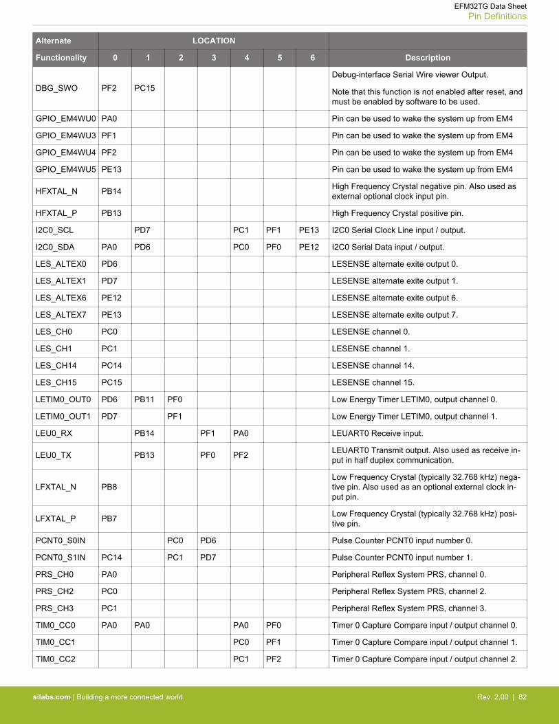
Alternate LOCATION
Functionality 0 1 2 3 4 5 6 Description
DBG_SWO PF2 PC15Debug-interface Serial Wire viewer Output.
Note that this function is not enabled after reset, andmust be enabled by software to be used.
GPIO_EM4WU0 PA0 Pin can be used to wake the system up from EM4
GPIO_EM4WU3 PF1 Pin can be used to wake the system up from EM4
GPIO_EM4WU4 PF2 Pin can be used to wake the system up from EM4
GPIO_EM4WU5 PE13 Pin can be used to wake the system up from EM4
HFXTAL_N PB14 High Frequency Crystal negative pin. Also used asexternal optional clock input pin.
HFXTAL_P PB13 High Frequency Crystal positive pin.
I2C0_SCL PD7 PC1 PF1 PE13 I2C0 Serial Clock Line input / output.
I2C0_SDA PA0 PD6 PC0 PF0 PE12 I2C0 Serial Data input / output.
LES_ALTEX0 PD6 LESENSE alternate exite output 0.
LES_ALTEX1 PD7 LESENSE alternate exite output 1.
LES_ALTEX6 PE12 LESENSE alternate exite output 6.
LES_ALTEX7 PE13 LESENSE alternate exite output 7.
LES_CH0 PC0 LESENSE channel 0.
LES_CH1 PC1 LESENSE channel 1.
LES_CH14 PC14 LESENSE channel 14.
LES_CH15 PC15 LESENSE channel 15.
LETIM0_OUT0 PD6 PB11 PF0 Low Energy Timer LETIM0, output channel 0.
LETIM0_OUT1 PD7 PF1 Low Energy Timer LETIM0, output channel 1.
LEU0_RX PB14 PF1 PA0 LEUART0 Receive input.
LEU0_TX PB13 PF0 PF2 LEUART0 Transmit output. Also used as receive in-put in half duplex communication.
LFXTAL_N PB8Low Frequency Crystal (typically 32.768 kHz) nega-tive pin. Also used as an optional external clock in-put pin.
LFXTAL_P PB7 Low Frequency Crystal (typically 32.768 kHz) posi-tive pin.
PCNT0_S0IN PC0 PD6 Pulse Counter PCNT0 input number 0.
PCNT0_S1IN PC14 PC1 PD7 Pulse Counter PCNT0 input number 1.
PRS_CH0 PA0 Peripheral Reflex System PRS, channel 0.
PRS_CH2 PC0 Peripheral Reflex System PRS, channel 2.
PRS_CH3 PC1 Peripheral Reflex System PRS, channel 3.
TIM0_CC0 PA0 PA0 PA0 PF0 Timer 0 Capture Compare input / output channel 0.
TIM0_CC1 PC0 PF1 Timer 0 Capture Compare input / output channel 1.
TIM0_CC2 PC1 PF2 Timer 0 Capture Compare input / output channel 2.
EFM32TG Data SheetPin Definitions
silabs.com | Building a more connected world. Rev. 2.00 | 82
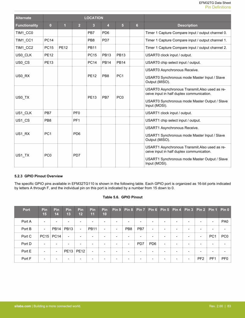
Alternate LOCATION
Functionality 0 1 2 3 4 5 6 Description
TIM1_CC0 PB7 PD6 Timer 1 Capture Compare input / output channel 0.
TIM1_CC1 PC14 PB8 PD7 Timer 1 Capture Compare input / output channel 1.
TIM1_CC2 PC15 PE12 PB11 Timer 1 Capture Compare input / output channel 2.
US0_CLK PE12 PC15 PB13 PB13 USART0 clock input / output.
US0_CS PE13 PC14 PB14 PB14 USART0 chip select input / output.
US0_RX PE12 PB8 PC1USART0 Asynchronous Receive.
USART0 Synchronous mode Master Input / SlaveOutput (MISO).
US0_TX PE13 PB7 PC0
USART0 Asynchronous Transmit.Also used as re-ceive input in half duplex communication.
USART0 Synchronous mode Master Output / SlaveInput (MOSI).
US1_CLK PB7 PF0 USART1 clock input / output.
US1_CS PB8 PF1 USART1 chip select input / output.
US1_RX PC1 PD6USART1 Asynchronous Receive.
USART1 Synchronous mode Master Input / SlaveOutput (MISO).
US1_TX PC0 PD7
USART1 Asynchronous Transmit.Also used as re-ceive input in half duplex communication.
USART1 Synchronous mode Master Output / SlaveInput (MOSI).
5.2.3 GPIO Pinout Overview
The specific GPIO pins available in EFM32TG110 is shown in the following table. Each GPIO port is organized as 16-bit ports indicatedby letters A through F, and the individual pin on this port is indicated by a number from 15 down to 0.
Table 5.6. GPIO Pinout
Port Pin15
Pin14
Pin13
Pin12
Pin11
Pin10
Pin 9 Pin 8 Pin 7 Pin 6 Pin 5 Pin 4 Pin 3 Pin 2 Pin 1 Pin 0
Port A - - - - - - - - - - - - - - - PA0
Port B - PB14 PB13 - PB11 - - PB8 PB7 - - - - - - -
Port C PC15 PC14 - - - - - - - - - - - - PC1 PC0
Port D - - - - - - - - PD7 PD6 - - - - - -
Port E - - PE13 PE12 - - - - - - - - - - - -
Port F - - - - - - - - - - - - - PF2 PF1 PF0
EFM32TG Data SheetPin Definitions
silabs.com | Building a more connected world. Rev. 2.00 | 83
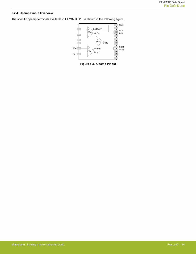
5.2.4 Opamp Pinout Overview
The specific opamp terminals available in EFM32TG110 is shown in the following figure.
-
+OPA0
-
+OPA2
-
+OPA1
OUT0ALT
OUT0
OUT2
OUT1ALT
OUT1
PD6
PD7
PB11
PC0PC1
PC14PC15
Figure 5.3. Opamp Pinout
EFM32TG Data SheetPin Definitions
silabs.com | Building a more connected world. Rev. 2.00 | 84
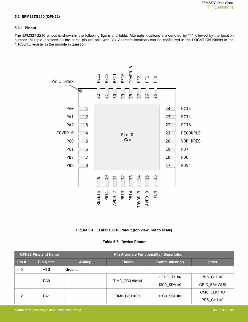
5.3 EFM32TG210 (QFN32)
5.3.1 Pinout
The EFM32TG210 pinout is shown in the following figure and table. Alternate locations are denoted by "#" followed by the locationnumber (Multiple locations on the same pin are split with "/"). Alternate locations can be configured in the LOCATION bitfield in the*_ROUTE register in the module in question.
Figure 5.4. EFM32TG210 Pinout (top view, not to scale)
Table 5.7. Device Pinout
QFN32 Pin# and Name Pin Alternate Functionality / Description
Pin # Pin Name Analog Timers Communication Other
0 VSS Ground.
1 PA0 TIM0_CC0 #0/1/4LEU0_RX #4
I2C0_SDA #0
PRS_CH0 #0
GPIO_EM4WU0
2 PA1 TIM0_CC1 #0/1 I2C0_SCL #0CMU_CLK1 #0
PRS_CH1 #0
EFM32TG Data SheetPin Definitions
silabs.com | Building a more connected world. Rev. 2.00 | 85
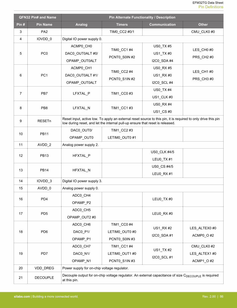
QFN32 Pin# and Name Pin Alternate Functionality / Description
Pin # Pin Name Analog Timers Communication Other
3 PA2 TIM0_CC2 #0/1 CMU_CLK0 #0
4 IOVDD_0 Digital IO power supply 0.
5 PC0
ACMP0_CH0
DAC0_OUT0ALT #0/
OPAMP_OUT0ALT
TIM0_CC1 #4
PCNT0_S0IN #2
US0_TX #5
US1_TX #0
I2C0_SDA #4
LES_CH0 #0
PRS_CH2 #0
6 PC1
ACMP0_CH1
DAC0_OUT0ALT #1/
OPAMP_OUT0ALT
TIM0_CC2 #4
PCNT0_S1IN #2
US0_RX #5
US1_RX #0
I2C0_SCL #4
LES_CH1 #0
PRS_CH3 #0
7 PB7 LFXTAL_P TIM1_CC0 #3US0_TX #4
US1_CLK #0
8 PB8 LFXTAL_N TIM1_CC1 #3US0_RX #4
US1_CS #0
9 RESETn Reset input, active low. To apply an external reset source to this pin, it is required to only drive this pinlow during reset, and let the internal pull-up ensure that reset is released.
10 PB11DAC0_OUT0/
OPAMP_OUT0
TIM1_CC2 #3
LETIM0_OUT0 #1
11 AVDD_2 Analog power supply 2.
12 PB13 HFXTAL_PUS0_CLK #4/5
LEU0_TX #1
13 PB14 HFXTAL_NUS0_CS #4/5
LEU0_RX #1
14 IOVDD_3 Digital IO power supply 3.
15 AVDD_0 Analog power supply 0.
16 PD4ADC0_CH4
OPAMP_P2LEU0_TX #0
17 PD5ADC0_CH5
OPAMP_OUT2 #0LEU0_RX #0
18 PD6
ADC0_CH6
DAC0_P1/
OPAMP_P1
TIM1_CC0 #4
LETIM0_OUT0 #0
PCNT0_S0IN #3
US1_RX #2
I2C0_SDA #1
LES_ALTEX0 #0
ACMP0_O #2
19 PD7
ADC0_CH7
DAC0_N1/
OPAMP_N1
TIM1_CC1 #4
LETIM0_OUT1 #0
PCNT0_S1IN #3
US1_TX #2
I2C0_SCL #1
CMU_CLK0 #2
LES_ALTEX1 #0
ACMP1_O #2
20 VDD_DREG Power supply for on-chip voltage regulator.
21 DECOUPLEDecouple output for on-chip voltage regulator. An external capacitance of size CDECOUPLE is requiredat this pin.
EFM32TG Data SheetPin Definitions
silabs.com | Building a more connected world. Rev. 2.00 | 86
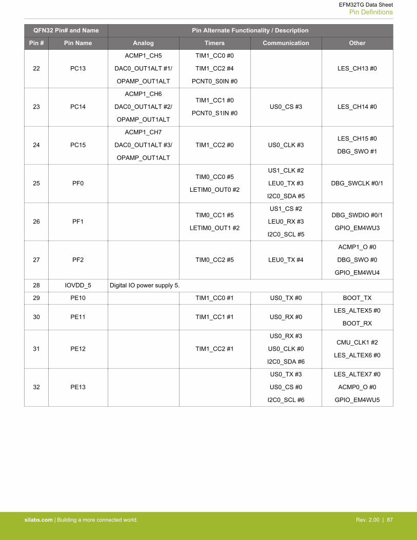
QFN32 Pin# and Name Pin Alternate Functionality / Description
Pin # Pin Name Analog Timers Communication Other
22 PC13
ACMP1_CH5
DAC0_OUT1ALT #1/
OPAMP_OUT1ALT
TIM1_CC0 #0
TIM1_CC2 #4
PCNT0_S0IN #0
LES_CH13 #0
23 PC14
ACMP1_CH6
DAC0_OUT1ALT #2/
OPAMP_OUT1ALT
TIM1_CC1 #0
PCNT0_S1IN #0US0_CS #3 LES_CH14 #0
24 PC15
ACMP1_CH7
DAC0_OUT1ALT #3/
OPAMP_OUT1ALT
TIM1_CC2 #0 US0_CLK #3LES_CH15 #0
DBG_SWO #1
25 PF0TIM0_CC0 #5
LETIM0_OUT0 #2
US1_CLK #2
LEU0_TX #3
I2C0_SDA #5
DBG_SWCLK #0/1
26 PF1TIM0_CC1 #5
LETIM0_OUT1 #2
US1_CS #2
LEU0_RX #3
I2C0_SCL #5
DBG_SWDIO #0/1
GPIO_EM4WU3
27 PF2 TIM0_CC2 #5 LEU0_TX #4
ACMP1_O #0
DBG_SWO #0
GPIO_EM4WU4
28 IOVDD_5 Digital IO power supply 5.
29 PE10 TIM1_CC0 #1 US0_TX #0 BOOT_TX
30 PE11 TIM1_CC1 #1 US0_RX #0LES_ALTEX5 #0
BOOT_RX
31 PE12 TIM1_CC2 #1
US0_RX #3
US0_CLK #0
I2C0_SDA #6
CMU_CLK1 #2
LES_ALTEX6 #0
32 PE13
US0_TX #3
US0_CS #0
I2C0_SCL #6
LES_ALTEX7 #0
ACMP0_O #0
GPIO_EM4WU5
EFM32TG Data SheetPin Definitions
silabs.com | Building a more connected world. Rev. 2.00 | 87
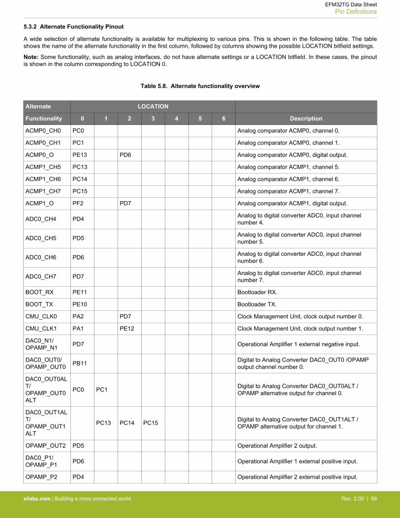
5.3.2 Alternate Functionality Pinout
A wide selection of alternate functionality is available for multiplexing to various pins. This is shown in the following table. The tableshows the name of the alternate functionality in the first column, followed by columns showing the possible LOCATION bitfield settings.
Note: Some functionality, such as analog interfaces, do not have alternate settings or a LOCATION bitfield. In these cases, the pinoutis shown in the column corresponding to LOCATION 0.
Table 5.8. Alternate functionality overview
Alternate LOCATION
Functionality 0 1 2 3 4 5 6 Description
ACMP0_CH0 PC0 Analog comparator ACMP0, channel 0.
ACMP0_CH1 PC1 Analog comparator ACMP0, channel 1.
ACMP0_O PE13 PD6 Analog comparator ACMP0, digital output.
ACMP1_CH5 PC13 Analog comparator ACMP1, channel 5.
ACMP1_CH6 PC14 Analog comparator ACMP1, channel 6.
ACMP1_CH7 PC15 Analog comparator ACMP1, channel 7.
ACMP1_O PF2 PD7 Analog comparator ACMP1, digital output.
ADC0_CH4 PD4 Analog to digital converter ADC0, input channelnumber 4.
ADC0_CH5 PD5 Analog to digital converter ADC0, input channelnumber 5.
ADC0_CH6 PD6 Analog to digital converter ADC0, input channelnumber 6.
ADC0_CH7 PD7 Analog to digital converter ADC0, input channelnumber 7.
BOOT_RX PE11 Bootloader RX.
BOOT_TX PE10 Bootloader TX.
CMU_CLK0 PA2 PD7 Clock Management Unit, clock output number 0.
CMU_CLK1 PA1 PE12 Clock Management Unit, clock output number 1.
DAC0_N1/OPAMP_N1 PD7 Operational Amplifier 1 external negative input.
DAC0_OUT0/OPAMP_OUT0 PB11 Digital to Analog Converter DAC0_OUT0 /OPAMP
output channel number 0.
DAC0_OUT0ALT/OPAMP_OUT0ALT
PC0 PC1 Digital to Analog Converter DAC0_OUT0ALT /OPAMP alternative output for channel 0.
DAC0_OUT1ALT/OPAMP_OUT1ALT
PC13 PC14 PC15 Digital to Analog Converter DAC0_OUT1ALT /OPAMP alternative output for channel 1.
OPAMP_OUT2 PD5 Operational Amplifier 2 output.
DAC0_P1/OPAMP_P1 PD6 Operational Amplifier 1 external positive input.
OPAMP_P2 PD4 Operational Amplifier 2 external positive input.
EFM32TG Data SheetPin Definitions
silabs.com | Building a more connected world. Rev. 2.00 | 88
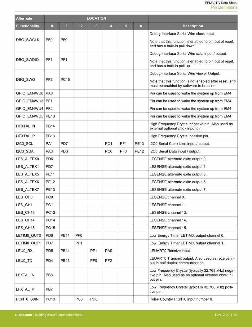
Alternate LOCATION
Functionality 0 1 2 3 4 5 6 Description
DBG_SWCLK PF0 PF0Debug-interface Serial Wire clock input.
Note that this function is enabled to pin out of reset,and has a built-in pull down.
DBG_SWDIO PF1 PF1Debug-interface Serial Wire data input / output.
Note that this function is enabled to pin out of reset,and has a built-in pull up.
DBG_SWO PF2 PC15Debug-interface Serial Wire viewer Output.
Note that this function is not enabled after reset, andmust be enabled by software to be used.
GPIO_EM4WU0 PA0 Pin can be used to wake the system up from EM4
GPIO_EM4WU3 PF1 Pin can be used to wake the system up from EM4
GPIO_EM4WU4 PF2 Pin can be used to wake the system up from EM4
GPIO_EM4WU5 PE13 Pin can be used to wake the system up from EM4
HFXTAL_N PB14 High Frequency Crystal negative pin. Also used asexternal optional clock input pin.
HFXTAL_P PB13 High Frequency Crystal positive pin.
I2C0_SCL PA1 PD7 PC1 PF1 PE13 I2C0 Serial Clock Line input / output.
I2C0_SDA PA0 PD6 PC0 PF0 PE12 I2C0 Serial Data input / output.
LES_ALTEX0 PD6 LESENSE alternate exite output 0.
LES_ALTEX1 PD7 LESENSE alternate exite output 1.
LES_ALTEX5 PE11 LESENSE alternate exite output 5.
LES_ALTEX6 PE12 LESENSE alternate exite output 6.
LES_ALTEX7 PE13 LESENSE alternate exite output 7.
LES_CH0 PC0 LESENSE channel 0.
LES_CH1 PC1 LESENSE channel 1.
LES_CH13 PC13 LESENSE channel 13.
LES_CH14 PC14 LESENSE channel 14.
LES_CH15 PC15 LESENSE channel 15.
LETIM0_OUT0 PD6 PB11 PF0 Low Energy Timer LETIM0, output channel 0.
LETIM0_OUT1 PD7 PF1 Low Energy Timer LETIM0, output channel 1.
LEU0_RX PD5 PB14 PF1 PA0 LEUART0 Receive input.
LEU0_TX PD4 PB13 PF0 PF2 LEUART0 Transmit output. Also used as receive in-put in half duplex communication.
LFXTAL_N PB8Low Frequency Crystal (typically 32.768 kHz) nega-tive pin. Also used as an optional external clock in-put pin.
LFXTAL_P PB7 Low Frequency Crystal (typically 32.768 kHz) posi-tive pin.
PCNT0_S0IN PC13 PC0 PD6 Pulse Counter PCNT0 input number 0.
EFM32TG Data SheetPin Definitions
silabs.com | Building a more connected world. Rev. 2.00 | 89
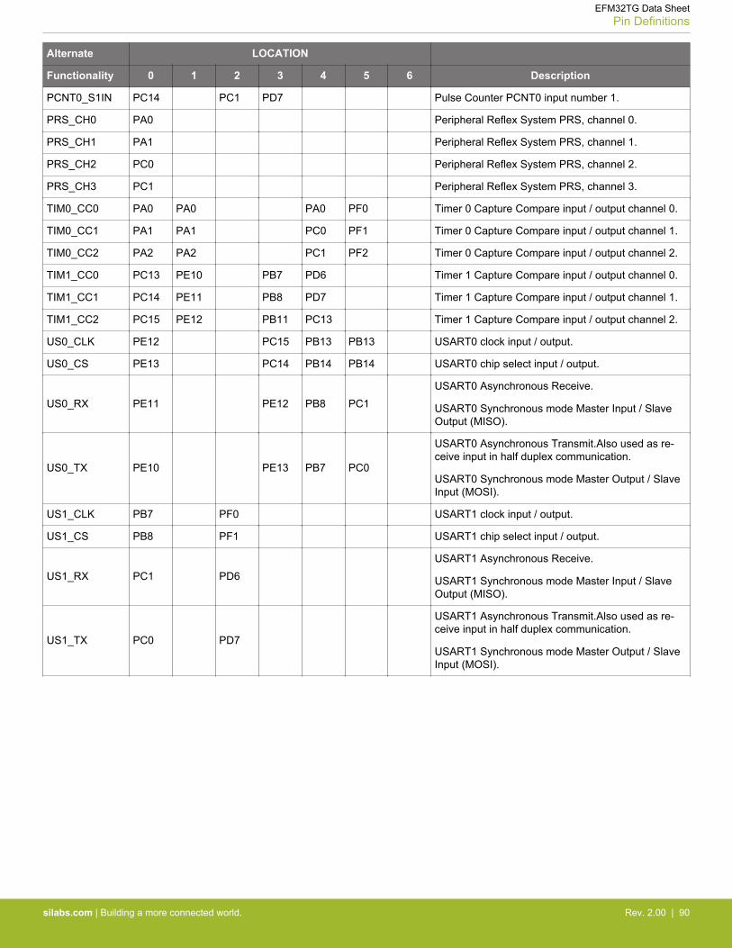
Alternate LOCATION
Functionality 0 1 2 3 4 5 6 Description
PCNT0_S1IN PC14 PC1 PD7 Pulse Counter PCNT0 input number 1.
PRS_CH0 PA0 Peripheral Reflex System PRS, channel 0.
PRS_CH1 PA1 Peripheral Reflex System PRS, channel 1.
PRS_CH2 PC0 Peripheral Reflex System PRS, channel 2.
PRS_CH3 PC1 Peripheral Reflex System PRS, channel 3.
TIM0_CC0 PA0 PA0 PA0 PF0 Timer 0 Capture Compare input / output channel 0.
TIM0_CC1 PA1 PA1 PC0 PF1 Timer 0 Capture Compare input / output channel 1.
TIM0_CC2 PA2 PA2 PC1 PF2 Timer 0 Capture Compare input / output channel 2.
TIM1_CC0 PC13 PE10 PB7 PD6 Timer 1 Capture Compare input / output channel 0.
TIM1_CC1 PC14 PE11 PB8 PD7 Timer 1 Capture Compare input / output channel 1.
TIM1_CC2 PC15 PE12 PB11 PC13 Timer 1 Capture Compare input / output channel 2.
US0_CLK PE12 PC15 PB13 PB13 USART0 clock input / output.
US0_CS PE13 PC14 PB14 PB14 USART0 chip select input / output.
US0_RX PE11 PE12 PB8 PC1USART0 Asynchronous Receive.
USART0 Synchronous mode Master Input / SlaveOutput (MISO).
US0_TX PE10 PE13 PB7 PC0
USART0 Asynchronous Transmit.Also used as re-ceive input in half duplex communication.
USART0 Synchronous mode Master Output / SlaveInput (MOSI).
US1_CLK PB7 PF0 USART1 clock input / output.
US1_CS PB8 PF1 USART1 chip select input / output.
US1_RX PC1 PD6USART1 Asynchronous Receive.
USART1 Synchronous mode Master Input / SlaveOutput (MISO).
US1_TX PC0 PD7
USART1 Asynchronous Transmit.Also used as re-ceive input in half duplex communication.
USART1 Synchronous mode Master Output / SlaveInput (MOSI).
EFM32TG Data SheetPin Definitions
silabs.com | Building a more connected world. Rev. 2.00 | 90
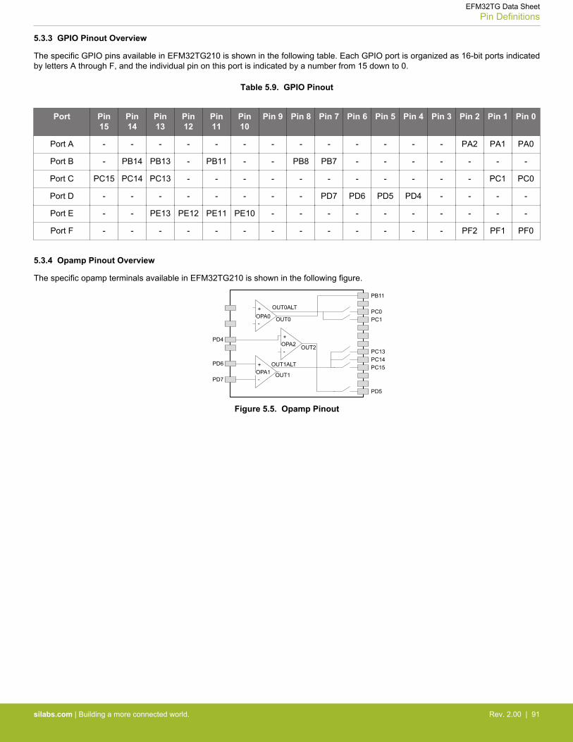
5.3.3 GPIO Pinout Overview
The specific GPIO pins available in EFM32TG210 is shown in the following table. Each GPIO port is organized as 16-bit ports indicatedby letters A through F, and the individual pin on this port is indicated by a number from 15 down to 0.
Table 5.9. GPIO Pinout
Port Pin15
Pin14
Pin13
Pin12
Pin11
Pin10
Pin 9 Pin 8 Pin 7 Pin 6 Pin 5 Pin 4 Pin 3 Pin 2 Pin 1 Pin 0
Port A - - - - - - - - - - - - - PA2 PA1 PA0
Port B - PB14 PB13 - PB11 - - PB8 PB7 - - - - - - -
Port C PC15 PC14 PC13 - - - - - - - - - - - PC1 PC0
Port D - - - - - - - - PD7 PD6 PD5 PD4 - - - -
Port E - - PE13 PE12 PE11 PE10 - - - - - - - - - -
Port F - - - - - - - - - - - - - PF2 PF1 PF0
5.3.4 Opamp Pinout Overview
The specific opamp terminals available in EFM32TG210 is shown in the following figure.
-
+OPA0
-
+OPA2
-
+OPA1
OUT0ALT
OUT0
OUT2
OUT1ALT
OUT1
PD4
PD6
PD7
PB11
PC0PC1
PC13PC14PC15
PD5
Figure 5.5. Opamp Pinout
EFM32TG Data SheetPin Definitions
silabs.com | Building a more connected world. Rev. 2.00 | 91
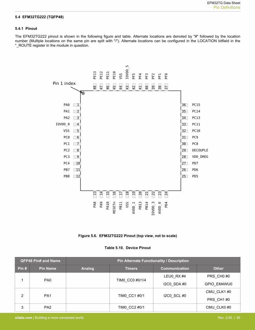
5.4 EFM32TG222 (TQFP48)
5.4.1 Pinout
The EFM32TG222 pinout is shown in the following figure and table. Alternate locations are denoted by "#" followed by the locationnumber (Multiple locations on the same pin are split with "/"). Alternate locations can be configured in the LOCATION bitfield in the*_ROUTE register in the module in question.
Figure 5.6. EFM32TG222 Pinout (top view, not to scale)
Table 5.10. Device Pinout
QFP48 Pin# and Name Pin Alternate Functionality / Description
Pin # Pin Name Analog Timers Communication Other
1 PA0 TIM0_CC0 #0/1/4LEU0_RX #4
I2C0_SDA #0
PRS_CH0 #0
GPIO_EM4WU0
2 PA1 TIM0_CC1 #0/1 I2C0_SCL #0CMU_CLK1 #0
PRS_CH1 #0
3 PA2 TIM0_CC2 #0/1 CMU_CLK0 #0
EFM32TG Data SheetPin Definitions
silabs.com | Building a more connected world. Rev. 2.00 | 92
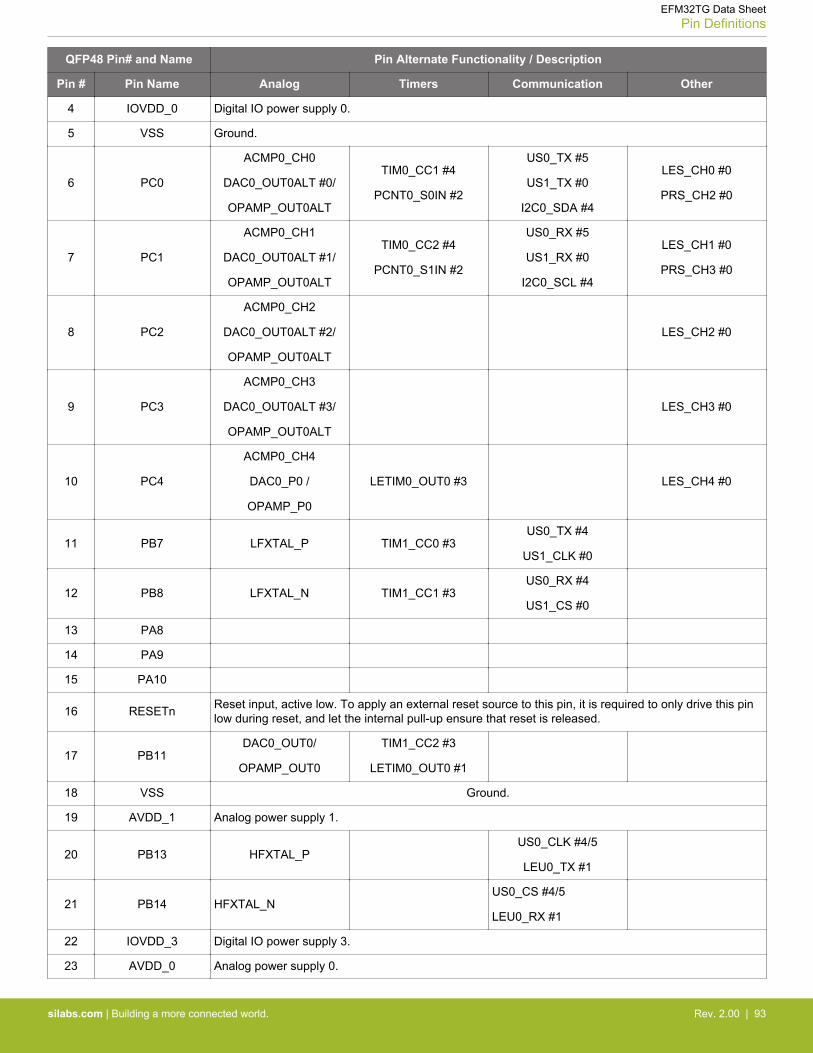
QFP48 Pin# and Name Pin Alternate Functionality / Description
Pin # Pin Name Analog Timers Communication Other
4 IOVDD_0 Digital IO power supply 0.
5 VSS Ground.
6 PC0
ACMP0_CH0
DAC0_OUT0ALT #0/
OPAMP_OUT0ALT
TIM0_CC1 #4
PCNT0_S0IN #2
US0_TX #5
US1_TX #0
I2C0_SDA #4
LES_CH0 #0
PRS_CH2 #0
7 PC1
ACMP0_CH1
DAC0_OUT0ALT #1/
OPAMP_OUT0ALT
TIM0_CC2 #4
PCNT0_S1IN #2
US0_RX #5
US1_RX #0
I2C0_SCL #4
LES_CH1 #0
PRS_CH3 #0
8 PC2
ACMP0_CH2
DAC0_OUT0ALT #2/
OPAMP_OUT0ALT
LES_CH2 #0
9 PC3
ACMP0_CH3
DAC0_OUT0ALT #3/
OPAMP_OUT0ALT
LES_CH3 #0
10 PC4
ACMP0_CH4
DAC0_P0 /
OPAMP_P0
LETIM0_OUT0 #3 LES_CH4 #0
11 PB7 LFXTAL_P TIM1_CC0 #3US0_TX #4
US1_CLK #0
12 PB8 LFXTAL_N TIM1_CC1 #3US0_RX #4
US1_CS #0
13 PA8
14 PA9
15 PA10
16 RESETn Reset input, active low. To apply an external reset source to this pin, it is required to only drive this pinlow during reset, and let the internal pull-up ensure that reset is released.
17 PB11DAC0_OUT0/
OPAMP_OUT0
TIM1_CC2 #3
LETIM0_OUT0 #1
18 VSS Ground.
19 AVDD_1 Analog power supply 1.
20 PB13 HFXTAL_PUS0_CLK #4/5
LEU0_TX #1
21 PB14 HFXTAL_NUS0_CS #4/5
LEU0_RX #1
22 IOVDD_3 Digital IO power supply 3.
23 AVDD_0 Analog power supply 0.
EFM32TG Data SheetPin Definitions
silabs.com | Building a more connected world. Rev. 2.00 | 93
QFP48 Pin# and Name Pin Alternate Functionality / Description
Pin # Pin Name Analog Timers Communication Other
24 PD4ADC0_CH4
OPAMP_P2LEU0_TX #0
25 PD5ADC0_CH5
OPAMP_OUT2 #0LEU0_RX #0
26 PD6
ADC0_CH6
DAC0_P1/
OPAMP_P1
TIM1_CC0 #4
LETIM0_OUT0 #0
PCNT0_S0IN #3
US1_RX #2
I2C0_SDA #1
LES_ALTEX0 #0
ACMP0_O #2
27 PD7
ADC0_CH7
DAC0_N1/
OPAMP_N1
TIM1_CC1 #4
LETIM0_OUT1 #0
PCNT0_S1IN #3
US1_TX #2
I2C0_SCL #1
CMU_CLK0 #2
LES_ALTEX1 #0
ACMP1_O #2
28 VDD_DREG Power supply for on-chip voltage regulator.
29 DECOUPLEDecouple output for on-chip voltage regulator. An external capacitance of size CDECOUPLE is requiredat this pin.
30 PC8 ACMP1_CH0 US0_CS #2 LES_CH8 #0
31 PC9 ACMP1_CH1 US0_CLK #2LES_CH9 #0
GPIO_EM4WU2
32 PC10 ACMP1_CH2 US0_RX #2 LES_CH10 #0
33 PC11 ACMP1_CH3 US0_TX #2 LES_CH11 #0
34 PC13
ACMP1_CH5
DAC0_OUT1ALT #1/
OPAMP_OUT1ALT
TIM1_CC0 #0
TIM1_CC2 #4
PCNT0_S0IN #0
LES_CH13 #0
35 PC14
ACMP1_CH6
DAC0_OUT1ALT #2/
OPAMP_OUT1ALT
TIM1_CC1 #0
PCNT0_S1IN #0US0_CS #3 LES_CH14 #0
36 PC15
ACMP1_CH7
DAC0_OUT1ALT #3/
OPAMP_OUT1ALT
TIM1_CC2 #0 US0_CLK #3LES_CH15 #0
DBG_SWO #1
37 PF0TIM0_CC0 #5
LETIM0_OUT0 #2
US1_CLK #2
LEU0_TX #3
I2C0_SDA #5
DBG_SWCLK #0/1
38 PF1TIM0_CC1 #5
LETIM0_OUT1 #2
US1_CS #2
LEU0_RX #3
I2C0_SCL #5
DBG_SWDIO #0/1
GPIO_EM4WU3
39 PF2 TIM0_CC2 #5 LEU0_TX #4
ACMP1_O #0
DBG_SWO #0
GPIO_EM4WU4
EFM32TG Data SheetPin Definitions
silabs.com | Building a more connected world. Rev. 2.00 | 94
QFP48 Pin# and Name Pin Alternate Functionality / Description
Pin # Pin Name Analog Timers Communication Other
40 PF3 PRS_CH0 #1
41 PF4 PRS_CH1 #1
42 PF5 PRS_CH2 #1
43 IOVDD_5 Digital IO power supply 5.
44 VSS Ground.
45 PE10 TIM1_CC0 #1 US0_TX #0 BOOT_TX
46 PE11 TIM1_CC1 #1 US0_RX #0LES_ALTEX5 #0
BOOT_RX
47 PE12 TIM1_CC2 #1
US0_RX #3
US0_CLK #0
I2C0_SDA #6
CMU_CLK1 #2
LES_ALTEX6 #0
48 PE13
US0_TX #3
US0_CS #0
I2C0_SCL #6
LES_ALTEX7 #0
ACMP0_O #0
GPIO_EM4WU5
EFM32TG Data SheetPin Definitions
silabs.com | Building a more connected world. Rev. 2.00 | 95

5.4.2 Alternate Functionality Pinout
A wide selection of alternate functionality is available for multiplexing to various pins. This is shown in the following table. The tableshows the name of the alternate functionality in the first column, followed by columns showing the possible LOCATION bitfield settings.
Note: Some functionality, such as analog interfaces, do not have alternate settings or a LOCATION bitfield. In these cases, the pinoutis shown in the column corresponding to LOCATION 0.
Table 5.11. Alternate functionality overview
Alternate LOCATION
Functionality 0 1 2 3 4 5 6 Description
ACMP0_CH0 PC0 Analog comparator ACMP0, channel 0.
ACMP0_CH1 PC1 Analog comparator ACMP0, channel 1.
ACMP0_CH2 PC2 Analog comparator ACMP0, channel 2.
ACMP0_CH3 PC3 Analog comparator ACMP0, channel 3.
ACMP0_CH4 PC4 Analog comparator ACMP0, channel 4.
ACMP0_O PE13 PD6 Analog comparator ACMP0, digital output.
ACMP1_CH0 PC8 Analog comparator ACMP1, channel 0.
ACMP1_CH1 PC9 Analog comparator ACMP1, channel 1.
ACMP1_CH2 PC10 Analog comparator ACMP1, channel 2.
ACMP1_CH3 PC11 Analog comparator ACMP1, channel 3.
ACMP1_CH5 PC13 Analog comparator ACMP1, channel 5.
ACMP1_CH6 PC14 Analog comparator ACMP1, channel 6.
ACMP1_CH7 PC15 Analog comparator ACMP1, channel 7.
ACMP1_O PF2 PD7 Analog comparator ACMP1, digital output.
ADC0_CH4 PD4 Analog to digital converter ADC0, input channelnumber 4.
ADC0_CH5 PD5 Analog to digital converter ADC0, input channelnumber 5.
ADC0_CH6 PD6 Analog to digital converter ADC0, input channelnumber 6.
ADC0_CH7 PD7 Analog to digital converter ADC0, input channelnumber 7.
BOOT_RX PE11 Bootloader RX.
BOOT_TX PE10 Bootloader TX.
CMU_CLK0 PA2 PD7 Clock Management Unit, clock output number 0.
CMU_CLK1 PA1 PE12 Clock Management Unit, clock output number 1.
DAC0_N1/OPAMP_N1 PD7 Operational Amplifier 1 external negative input.
DAC0_OUT0/OPAMP_OUT0 PB11 Digital to Analog Converter DAC0_OUT0 /OPAMP
output channel number 0.
EFM32TG Data SheetPin Definitions
silabs.com | Building a more connected world. Rev. 2.00 | 96

Alternate LOCATION
Functionality 0 1 2 3 4 5 6 Description
DAC0_OUT0ALT/OPAMP_OUT0ALT
PC0 PC1 PC2 PC3 Digital to Analog Converter DAC0_OUT0ALT /OPAMP alternative output for channel 0.
DAC0_OUT1ALT/OPAMP_OUT1ALT
PC13 PC14 PC15 Digital to Analog Converter DAC0_OUT1ALT /OPAMP alternative output for channel 1.
OPAMP_OUT2 PD5 Operational Amplifier 2 output.
DAC0_P0/OPAMP_P0 PC4 Operational Amplifier 0 external positive input.
DAC0_P1/OPAMP_P1 PD6 Operational Amplifier 1 external positive input.
OPAMP_P2 PD4 Operational Amplifier 2 external positive input.
DBG_SWCLK PF0 PF0Debug-interface Serial Wire clock input.
Note that this function is enabled to pin out of reset,and has a built-in pull down.
DBG_SWDIO PF1 PF1Debug-interface Serial Wire data input / output.
Note that this function is enabled to pin out of reset,and has a built-in pull up.
DBG_SWO PF2 PC15Debug-interface Serial Wire viewer Output.
Note that this function is not enabled after reset, andmust be enabled by software to be used.
GPIO_EM4WU0 PA0 Pin can be used to wake the system up from EM4
GPIO_EM4WU2 PC9 Pin can be used to wake the system up from EM4
GPIO_EM4WU3 PF1 Pin can be used to wake the system up from EM4
GPIO_EM4WU4 PF2 Pin can be used to wake the system up from EM4
GPIO_EM4WU5 PE13 Pin can be used to wake the system up from EM4
HFXTAL_N PB14 High Frequency Crystal negative pin. Also used asexternal optional clock input pin.
HFXTAL_P PB13 High Frequency Crystal positive pin.
I2C0_SCL PA1 PD7 PC1 PF1 PE13 I2C0 Serial Clock Line input / output.
I2C0_SDA PA0 PD6 PC0 PF0 PE12 I2C0 Serial Data input / output.
LES_ALTEX0 PD6 LESENSE alternate exite output 0.
LES_ALTEX1 PD7 LESENSE alternate exite output 1.
LES_ALTEX5 PE11 LESENSE alternate exite output 5.
LES_ALTEX6 PE12 LESENSE alternate exite output 6.
LES_ALTEX7 PE13 LESENSE alternate exite output 7.
LES_CH0 PC0 LESENSE channel 0.
LES_CH1 PC1 LESENSE channel 1.
LES_CH2 PC2 LESENSE channel 2.
EFM32TG Data SheetPin Definitions
silabs.com | Building a more connected world. Rev. 2.00 | 97
Alternate LOCATION
Functionality 0 1 2 3 4 5 6 Description
LES_CH3 PC3 LESENSE channel 3.
LES_CH4 PC4 LESENSE channel 4.
LES_CH8 PC8 LESENSE channel 8.
LES_CH9 PC9 LESENSE channel 9.
LES_CH10 PC10 LESENSE channel 10.
LES_CH11 PC11 LESENSE channel 11.
LES_CH13 PC13 LESENSE channel 13.
LES_CH14 PC14 LESENSE channel 14.
LES_CH15 PC15 LESENSE channel 15.
LETIM0_OUT0 PD6 PB11 PF0 PC4 Low Energy Timer LETIM0, output channel 0.
LETIM0_OUT1 PD7 PF1 Low Energy Timer LETIM0, output channel 1.
LEU0_RX PD5 PB14 PF1 PA0 LEUART0 Receive input.
LEU0_TX PD4 PB13 PF0 PF2 LEUART0 Transmit output. Also used as receive in-put in half duplex communication.
LFXTAL_N PB8Low Frequency Crystal (typically 32.768 kHz) nega-tive pin. Also used as an optional external clock in-put pin.
LFXTAL_P PB7 Low Frequency Crystal (typically 32.768 kHz) posi-tive pin.
PCNT0_S0IN PC13 PC0 PD6 Pulse Counter PCNT0 input number 0.
PCNT0_S1IN PC14 PC1 PD7 Pulse Counter PCNT0 input number 1.
PRS_CH0 PA0 PF3 Peripheral Reflex System PRS, channel 0.
PRS_CH1 PA1 PF4 Peripheral Reflex System PRS, channel 1.
PRS_CH2 PC0 PF5 Peripheral Reflex System PRS, channel 2.
PRS_CH3 PC1 Peripheral Reflex System PRS, channel 3.
TIM0_CC0 PA0 PA0 PA0 PF0 Timer 0 Capture Compare input / output channel 0.
TIM0_CC1 PA1 PA1 PC0 PF1 Timer 0 Capture Compare input / output channel 1.
TIM0_CC2 PA2 PA2 PC1 PF2 Timer 0 Capture Compare input / output channel 2.
TIM1_CC0 PC13 PE10 PB7 PD6 Timer 1 Capture Compare input / output channel 0.
TIM1_CC1 PC14 PE11 PB8 PD7 Timer 1 Capture Compare input / output channel 1.
TIM1_CC2 PC15 PE12 PB11 PC13 Timer 1 Capture Compare input / output channel 2.
US0_CLK PE12 PC9 PC15 PB13 PB13 USART0 clock input / output.
US0_CS PE13 PC8 PC14 PB14 PB14 USART0 chip select input / output.
US0_RX PE11 PC10 PE12 PB8 PC1USART0 Asynchronous Receive.
USART0 Synchronous mode Master Input / SlaveOutput (MISO).
EFM32TG Data SheetPin Definitions
silabs.com | Building a more connected world. Rev. 2.00 | 98

Alternate LOCATION
Functionality 0 1 2 3 4 5 6 Description
US0_TX PE10 PC11 PE13 PB7 PC0
USART0 Asynchronous Transmit.Also used as re-ceive input in half duplex communication.
USART0 Synchronous mode Master Output / SlaveInput (MOSI).
US1_CLK PB7 PF0 USART1 clock input / output.
US1_CS PB8 PF1 USART1 chip select input / output.
US1_RX PC1 PD6USART1 Asynchronous Receive.
USART1 Synchronous mode Master Input / SlaveOutput (MISO).
US1_TX PC0 PD7
USART1 Asynchronous Transmit.Also used as re-ceive input in half duplex communication.
USART1 Synchronous mode Master Output / SlaveInput (MOSI).
5.4.3 GPIO Pinout Overview
The specific GPIO pins available in EFM32TG222 is shown in the following table. Each GPIO port is organized as 16-bit ports indicatedby letters A through F, and the individual pin on this port is indicated by a number from 15 down to 0.
Table 5.12. GPIO Pinout
Port Pin15
Pin14
Pin13
Pin12
Pin11
Pin10
Pin 9 Pin 8 Pin 7 Pin 6 Pin 5 Pin 4 Pin 3 Pin 2 Pin 1 Pin 0
Port A - - - - - PA10 PA9 PA8 - - - - - PA2 PA1 PA0
Port B - PB14 PB13 - PB11 - - PB8 PB7 - - - - - - -
Port C PC15 PC14 PC13 - PC11 PC10 PC9 PC8 - - - PC4 PC3 PC2 PC1 PC0
Port D - - - - - - - - PD7 PD6 PD5 PD4 - - - -
Port E - - PE13 PE12 PE11 PE10 - - - - - - - - - -
Port F - - - - - - - - - - PF5 PF4 PF3 PF2 PF1 PF0
5.4.4 Opamp Pinout Overview
The specific opamp terminals available in EFM32TG222 is shown in the following figure.
-
+OPA0
-
+OPA2
-
+OPA1
OUT0ALT
OUT0
OUT2
OUT1ALT
OUT1
PC4
PD4
PD6
PD7
PB11
PC0PC1PC2PC3
PC13PC14PC15
PD5
Figure 5.7. Opamp Pinout
EFM32TG Data SheetPin Definitions
silabs.com | Building a more connected world. Rev. 2.00 | 99
5.5 EFM32TG225 (BGA48)
5.5.1 Pinout
The EFM32TG225 pinout is shown in the following figure and table. Alternate locations are denoted by "#" followed by the locationnumber (Multiple locations on the same pin are split with "/"). Alternate locations can be configured in the LOCATION bitfield in the*_ROUTE register in the module in question.
Figure 5.8. EFM32TG225 Pinout (top view, not to scale)
Table 5.13. Device Pinout
BGA48 Pin# and Name Pin Alternate Functionality / Description
Pin # Pin Name Analog Timers Communication Other
A1 PE13
US0_TX #3
US0_CS #0
I2C0_SCL #6
LES_ALTEX7 #0
ACMP0_O #0
GPIO_EM4WU5
EFM32TG Data SheetPin Definitions
silabs.com | Building a more connected world. Rev. 2.00 | 100
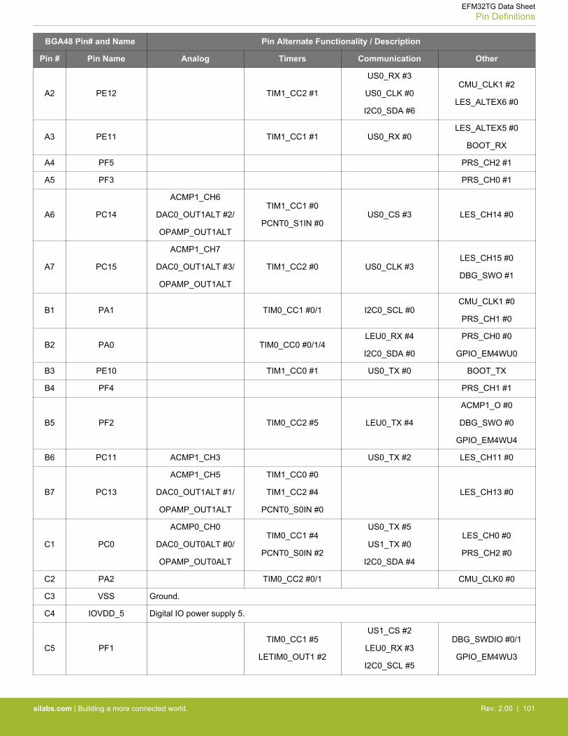
BGA48 Pin# and Name Pin Alternate Functionality / Description
Pin # Pin Name Analog Timers Communication Other
A2 PE12 TIM1_CC2 #1
US0_RX #3
US0_CLK #0
I2C0_SDA #6
CMU_CLK1 #2
LES_ALTEX6 #0
A3 PE11 TIM1_CC1 #1 US0_RX #0LES_ALTEX5 #0
BOOT_RX
A4 PF5 PRS_CH2 #1
A5 PF3 PRS_CH0 #1
A6 PC14
ACMP1_CH6
DAC0_OUT1ALT #2/
OPAMP_OUT1ALT
TIM1_CC1 #0
PCNT0_S1IN #0US0_CS #3 LES_CH14 #0
A7 PC15
ACMP1_CH7
DAC0_OUT1ALT #3/
OPAMP_OUT1ALT
TIM1_CC2 #0 US0_CLK #3LES_CH15 #0
DBG_SWO #1
B1 PA1 TIM0_CC1 #0/1 I2C0_SCL #0CMU_CLK1 #0
PRS_CH1 #0
B2 PA0 TIM0_CC0 #0/1/4LEU0_RX #4
I2C0_SDA #0
PRS_CH0 #0
GPIO_EM4WU0
B3 PE10 TIM1_CC0 #1 US0_TX #0 BOOT_TX
B4 PF4 PRS_CH1 #1
B5 PF2 TIM0_CC2 #5 LEU0_TX #4
ACMP1_O #0
DBG_SWO #0
GPIO_EM4WU4
B6 PC11 ACMP1_CH3 US0_TX #2 LES_CH11 #0
B7 PC13
ACMP1_CH5
DAC0_OUT1ALT #1/
OPAMP_OUT1ALT
TIM1_CC0 #0
TIM1_CC2 #4
PCNT0_S0IN #0
LES_CH13 #0
C1 PC0
ACMP0_CH0
DAC0_OUT0ALT #0/
OPAMP_OUT0ALT
TIM0_CC1 #4
PCNT0_S0IN #2
US0_TX #5
US1_TX #0
I2C0_SDA #4
LES_CH0 #0
PRS_CH2 #0
C2 PA2 TIM0_CC2 #0/1 CMU_CLK0 #0
C3 VSS Ground.
C4 IOVDD_5 Digital IO power supply 5.
C5 PF1TIM0_CC1 #5
LETIM0_OUT1 #2
US1_CS #2
LEU0_RX #3
I2C0_SCL #5
DBG_SWDIO #0/1
GPIO_EM4WU3
EFM32TG Data SheetPin Definitions
silabs.com | Building a more connected world. Rev. 2.00 | 101
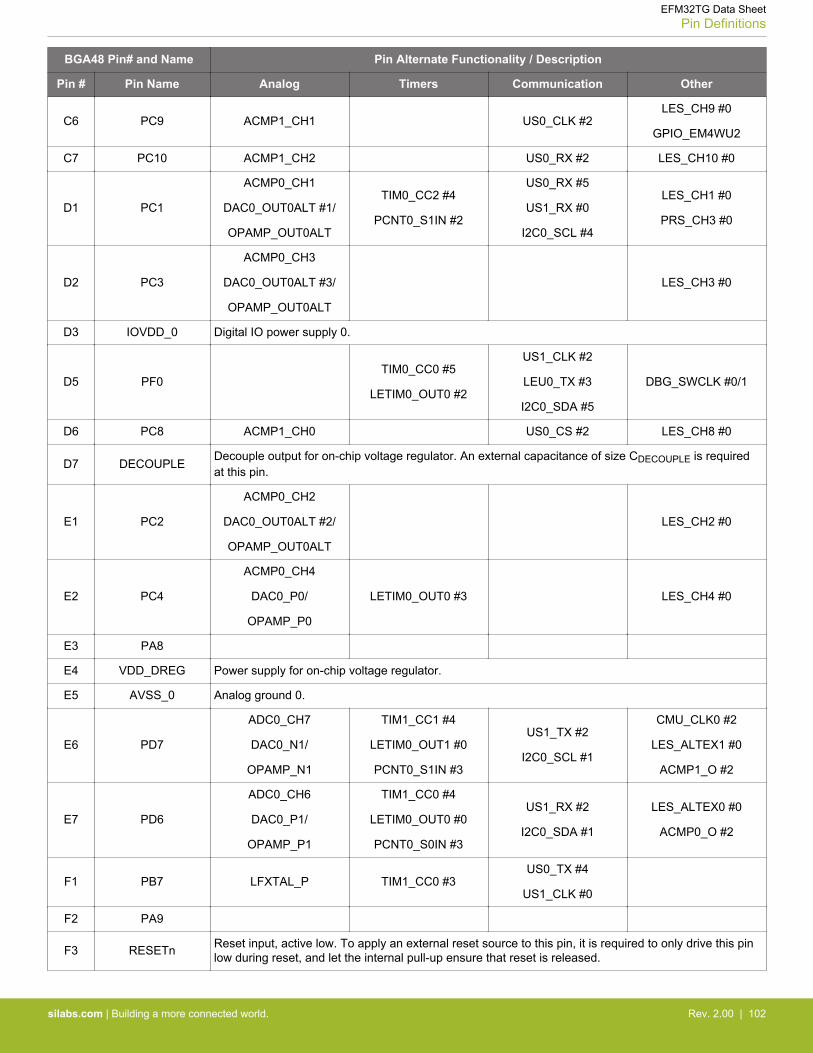
BGA48 Pin# and Name Pin Alternate Functionality / Description
Pin # Pin Name Analog Timers Communication Other
C6 PC9 ACMP1_CH1 US0_CLK #2LES_CH9 #0
GPIO_EM4WU2
C7 PC10 ACMP1_CH2 US0_RX #2 LES_CH10 #0
D1 PC1
ACMP0_CH1
DAC0_OUT0ALT #1/
OPAMP_OUT0ALT
TIM0_CC2 #4
PCNT0_S1IN #2
US0_RX #5
US1_RX #0
I2C0_SCL #4
LES_CH1 #0
PRS_CH3 #0
D2 PC3
ACMP0_CH3
DAC0_OUT0ALT #3/
OPAMP_OUT0ALT
LES_CH3 #0
D3 IOVDD_0 Digital IO power supply 0.
D5 PF0TIM0_CC0 #5
LETIM0_OUT0 #2
US1_CLK #2
LEU0_TX #3
I2C0_SDA #5
DBG_SWCLK #0/1
D6 PC8 ACMP1_CH0 US0_CS #2 LES_CH8 #0
D7 DECOUPLEDecouple output for on-chip voltage regulator. An external capacitance of size CDECOUPLE is requiredat this pin.
E1 PC2
ACMP0_CH2
DAC0_OUT0ALT #2/
OPAMP_OUT0ALT
LES_CH2 #0
E2 PC4
ACMP0_CH4
DAC0_P0/
OPAMP_P0
LETIM0_OUT0 #3 LES_CH4 #0
E3 PA8
E4 VDD_DREG Power supply for on-chip voltage regulator.
E5 AVSS_0 Analog ground 0.
E6 PD7
ADC0_CH7
DAC0_N1/
OPAMP_N1
TIM1_CC1 #4
LETIM0_OUT1 #0
PCNT0_S1IN #3
US1_TX #2
I2C0_SCL #1
CMU_CLK0 #2
LES_ALTEX1 #0
ACMP1_O #2
E7 PD6
ADC0_CH6
DAC0_P1/
OPAMP_P1
TIM1_CC0 #4
LETIM0_OUT0 #0
PCNT0_S0IN #3
US1_RX #2
I2C0_SDA #1
LES_ALTEX0 #0
ACMP0_O #2
F1 PB7 LFXTAL_P TIM1_CC0 #3US0_TX #4
US1_CLK #0
F2 PA9
F3 RESETn Reset input, active low. To apply an external reset source to this pin, it is required to only drive this pinlow during reset, and let the internal pull-up ensure that reset is released.
EFM32TG Data SheetPin Definitions
silabs.com | Building a more connected world. Rev. 2.00 | 102
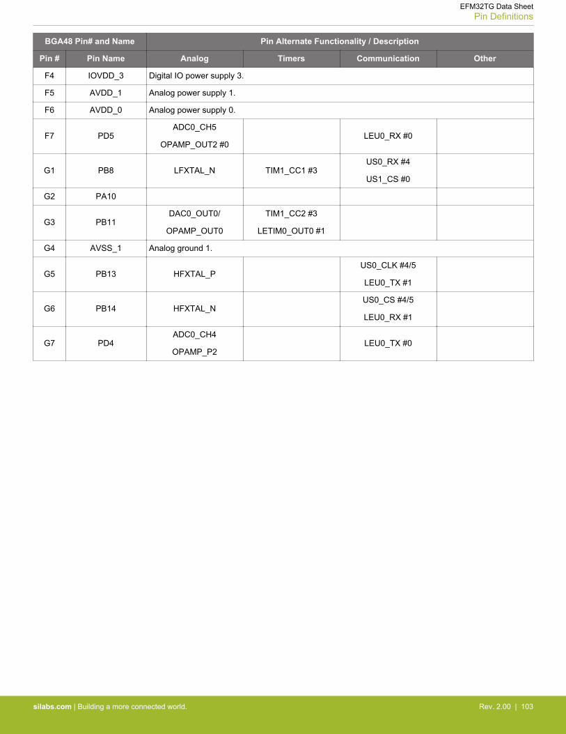
BGA48 Pin# and Name Pin Alternate Functionality / Description
Pin # Pin Name Analog Timers Communication Other
F4 IOVDD_3 Digital IO power supply 3.
F5 AVDD_1 Analog power supply 1.
F6 AVDD_0 Analog power supply 0.
F7 PD5ADC0_CH5
OPAMP_OUT2 #0LEU0_RX #0
G1 PB8 LFXTAL_N TIM1_CC1 #3US0_RX #4
US1_CS #0
G2 PA10
G3 PB11DAC0_OUT0/
OPAMP_OUT0
TIM1_CC2 #3
LETIM0_OUT0 #1
G4 AVSS_1 Analog ground 1.
G5 PB13 HFXTAL_PUS0_CLK #4/5
LEU0_TX #1
G6 PB14 HFXTAL_NUS0_CS #4/5
LEU0_RX #1
G7 PD4ADC0_CH4
OPAMP_P2LEU0_TX #0
EFM32TG Data SheetPin Definitions
silabs.com | Building a more connected world. Rev. 2.00 | 103
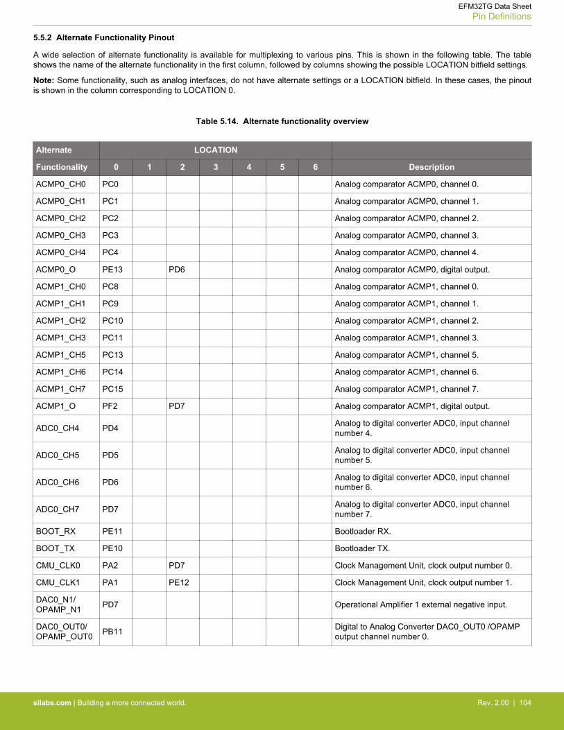
5.5.2 Alternate Functionality Pinout
A wide selection of alternate functionality is available for multiplexing to various pins. This is shown in the following table. The tableshows the name of the alternate functionality in the first column, followed by columns showing the possible LOCATION bitfield settings.
Note: Some functionality, such as analog interfaces, do not have alternate settings or a LOCATION bitfield. In these cases, the pinoutis shown in the column corresponding to LOCATION 0.
Table 5.14. Alternate functionality overview
Alternate LOCATION
Functionality 0 1 2 3 4 5 6 Description
ACMP0_CH0 PC0 Analog comparator ACMP0, channel 0.
ACMP0_CH1 PC1 Analog comparator ACMP0, channel 1.
ACMP0_CH2 PC2 Analog comparator ACMP0, channel 2.
ACMP0_CH3 PC3 Analog comparator ACMP0, channel 3.
ACMP0_CH4 PC4 Analog comparator ACMP0, channel 4.
ACMP0_O PE13 PD6 Analog comparator ACMP0, digital output.
ACMP1_CH0 PC8 Analog comparator ACMP1, channel 0.
ACMP1_CH1 PC9 Analog comparator ACMP1, channel 1.
ACMP1_CH2 PC10 Analog comparator ACMP1, channel 2.
ACMP1_CH3 PC11 Analog comparator ACMP1, channel 3.
ACMP1_CH5 PC13 Analog comparator ACMP1, channel 5.
ACMP1_CH6 PC14 Analog comparator ACMP1, channel 6.
ACMP1_CH7 PC15 Analog comparator ACMP1, channel 7.
ACMP1_O PF2 PD7 Analog comparator ACMP1, digital output.
ADC0_CH4 PD4 Analog to digital converter ADC0, input channelnumber 4.
ADC0_CH5 PD5 Analog to digital converter ADC0, input channelnumber 5.
ADC0_CH6 PD6 Analog to digital converter ADC0, input channelnumber 6.
ADC0_CH7 PD7 Analog to digital converter ADC0, input channelnumber 7.
BOOT_RX PE11 Bootloader RX.
BOOT_TX PE10 Bootloader TX.
CMU_CLK0 PA2 PD7 Clock Management Unit, clock output number 0.
CMU_CLK1 PA1 PE12 Clock Management Unit, clock output number 1.
DAC0_N1/OPAMP_N1 PD7 Operational Amplifier 1 external negative input.
DAC0_OUT0/OPAMP_OUT0 PB11 Digital to Analog Converter DAC0_OUT0 /OPAMP
output channel number 0.
EFM32TG Data SheetPin Definitions
silabs.com | Building a more connected world. Rev. 2.00 | 104
Alternate LOCATION
Functionality 0 1 2 3 4 5 6 Description
DAC0_OUT0ALT/OPAMP_OUT0ALT
PC0 PC1 PC2 PC3 Digital to Analog Converter DAC0_OUT0ALT /OPAMP alternative output for channel 0.
DAC0_OUT1ALT/OPAMP_OUT1ALT
PC13 PC14 PC15 Digital to Analog Converter DAC0_OUT1ALT /OPAMP alternative output for channel 1.
OPAMP_OUT2 PD5 Operational Amplifier 2 output.
DAC0_P0/OPAMP_P0 PC4 Operational Amplifier 0 external positive input.
DAC0_P1/OPAMP_P1 PD6 Operational Amplifier 1 external positive input.
OPAMP_P2 PD4 Operational Amplifier 2 external positive input.
DBG_SWCLK PF0 PF0Debug-interface Serial Wire clock input.
Note that this function is enabled to pin out of reset,and has a built-in pull down.
DBG_SWDIO PF1 PF1Debug-interface Serial Wire data input / output.
Note that this function is enabled to pin out of reset,and has a built-in pull up.
DBG_SWO PF2 PC15Debug-interface Serial Wire viewer Output.
Note that this function is not enabled after reset, andmust be enabled by software to be used.
GPIO_EM4WU0 PA0 Pin can be used to wake the system up from EM4
GPIO_EM4WU2 PC9 Pin can be used to wake the system up from EM4
GPIO_EM4WU3 PF1 Pin can be used to wake the system up from EM4
GPIO_EM4WU4 PF2 Pin can be used to wake the system up from EM4
GPIO_EM4WU5 PE13 Pin can be used to wake the system up from EM4
HFXTAL_N PB14 High Frequency Crystal negative pin. Also used asexternal optional clock input pin.
HFXTAL_P PB13 High Frequency Crystal positive pin.
I2C0_SCL PA1 PD7 PC1 PF1 PE13 I2C0 Serial Clock Line input / output.
I2C0_SDA PA0 PD6 PC0 PF0 PE12 I2C0 Serial Data input / output.
LES_ALTEX0 PD6 LESENSE alternate exite output 0.
LES_ALTEX1 PD7 LESENSE alternate exite output 1.
LES_ALTEX5 PE11 LESENSE alternate exite output 5.
LES_ALTEX6 PE12 LESENSE alternate exite output 6.
LES_ALTEX7 PE13 LESENSE alternate exite output 7.
LES_CH0 PC0 LESENSE channel 0.
LES_CH1 PC1 LESENSE channel 1.
LES_CH2 PC2 LESENSE channel 2.
EFM32TG Data SheetPin Definitions
silabs.com | Building a more connected world. Rev. 2.00 | 105

Alternate LOCATION
Functionality 0 1 2 3 4 5 6 Description
LES_CH3 PC3 LESENSE channel 3.
LES_CH4 PC4 LESENSE channel 4.
LES_CH8 PC8 LESENSE channel 8.
LES_CH9 PC9 LESENSE channel 9.
LES_CH10 PC10 LESENSE channel 10.
LES_CH11 PC11 LESENSE channel 11.
LES_CH13 PC13 LESENSE channel 13.
LES_CH14 PC14 LESENSE channel 14.
LES_CH15 PC15 LESENSE channel 15.
LETIM0_OUT0 PD6 PB11 PF0 PC4 Low Energy Timer LETIM0, output channel 0.
LETIM0_OUT1 PD7 PF1 Low Energy Timer LETIM0, output channel 1.
LEU0_RX PD5 PB14 PF1 PA0 LEUART0 Receive input.
LEU0_TX PD4 PB13 PF0 PF2 LEUART0 Transmit output. Also used as receive in-put in half duplex communication.
LFXTAL_N PB8Low Frequency Crystal (typically 32.768 kHz) nega-tive pin. Also used as an optional external clock in-put pin.
LFXTAL_P PB7 Low Frequency Crystal (typically 32.768 kHz) posi-tive pin.
PCNT0_S0IN PC13 PC0 PD6 Pulse Counter PCNT0 input number 0.
PCNT0_S1IN PC14 PC1 PD7 Pulse Counter PCNT0 input number 1.
PRS_CH0 PA0 PF3 Peripheral Reflex System PRS, channel 0.
PRS_CH1 PA1 PF4 Peripheral Reflex System PRS, channel 1.
PRS_CH2 PC0 PF5 Peripheral Reflex System PRS, channel 2.
PRS_CH3 PC1 Peripheral Reflex System PRS, channel 3.
TIM0_CC0 PA0 PA0 PA0 PF0 Timer 0 Capture Compare input / output channel 0.
TIM0_CC1 PA1 PA1 PC0 PF1 Timer 0 Capture Compare input / output channel 1.
TIM0_CC2 PA2 PA2 PC1 PF2 Timer 0 Capture Compare input / output channel 2.
TIM1_CC0 PC13 PE10 PB7 PD6 Timer 1 Capture Compare input / output channel 0.
TIM1_CC1 PC14 PE11 PB8 PD7 Timer 1 Capture Compare input / output channel 1.
TIM1_CC2 PC15 PE12 PB11 PC13 Timer 1 Capture Compare input / output channel 2.
US0_CLK PE12 PC9 PC15 PB13 PB13 USART0 clock input / output.
US0_CS PE13 PC8 PC14 PB14 PB14 USART0 chip select input / output.
US0_RX PE11 PC10 PE12 PB8 PC1USART0 Asynchronous Receive.
USART0 Synchronous mode Master Input / SlaveOutput (MISO).
EFM32TG Data SheetPin Definitions
silabs.com | Building a more connected world. Rev. 2.00 | 106
Alternate LOCATION
Functionality 0 1 2 3 4 5 6 Description
US0_TX PE10 PC11 PE13 PB7 PC0
USART0 Asynchronous Transmit.Also used as re-ceive input in half duplex communication.
USART0 Synchronous mode Master Output / SlaveInput (MOSI).
US1_CLK PB7 PF0 USART1 clock input / output.
US1_CS PB8 PF1 USART1 chip select input / output.
US1_RX PC1 PD6USART1 Asynchronous Receive.
USART1 Synchronous mode Master Input / SlaveOutput (MISO).
US1_TX PC0 PD7
USART1 Asynchronous Transmit.Also used as re-ceive input in half duplex communication.
USART1 Synchronous mode Master Output / SlaveInput (MOSI).
5.5.3 GPIO Pinout Overview
The specific GPIO pins available in EFM32TG225 is shown in the following table. Each GPIO port is organized as 16-bit ports indicatedby letters A through F, and the individual pin on this port is indicated by a number from 15 down to 0.
Table 5.15. GPIO Pinout
Port Pin15
Pin14
Pin13
Pin12
Pin11
Pin10
Pin 9 Pin 8 Pin 7 Pin 6 Pin 5 Pin 4 Pin 3 Pin 2 Pin 1 Pin 0
Port A - - - - - PA10 PA9 PA8 - - - - - PA2 PA1 PA0
Port B - PB14 PB13 - PB11 - - PB8 PB7 - - - - - - -
Port C PC15 PC14 PC13 - PC11 PC10 PC9 PC8 - - - PC4 PC3 PC2 PC1 PC0
Port D - - - - - - - - PD7 PD6 PD5 PD4 - - - -
Port E - - PE13 PE12 PE11 PE10 - - - - - - - - - -
Port F - - - - - - - - - - PF5 PF4 PF3 PF2 PF1 PF0
5.5.4 Opamp Pinout Overview
The specific opamp terminals available in EFM32TG225 is shown in the following figure.
-
+OPA0
-
+OPA2
-
+OPA1
OUT0ALT
OUT0
OUT2
OUT1ALT
OUT1
PC4
PD4
PD6
PD7
PB11
PC0PC1PC2PC3
PC13PC14PC15
PD5
Figure 5.9. Opamp Pinout
EFM32TG Data SheetPin Definitions
silabs.com | Building a more connected world. Rev. 2.00 | 107
5.6 EFM32TG230 (QFN64)
5.6.1 Pinout
The EFM32TG230 pinout is shown in the following figure and table. Alternate locations are denoted by "#" followed by the locationnumber (Multiple locations on the same pin are split with "/"). Alternate locations can be configured in the LOCATION bitfield in the*_ROUTE register in the module in question.
Figure 5.10. EFM32TG230 Pinout (top view, not to scale)
Table 5.16. Device Pinout
QFN64 Pin# and Name Pin Alternate Functionality / Description
Pin # Pin Name Analog Timers Communication Other
0 VSS Ground.
1 PA0 TIM0_CC0 #0/1/4LEU0_RX #4
I2C0_SDA #0
PRS_CH0 #0
GPIO_EM4WU0
2 PA1 TIM0_CC1 #0/1 I2C0_SCL #0CMU_CLK1 #0
PRS_CH1 #0
EFM32TG Data SheetPin Definitions
silabs.com | Building a more connected world. Rev. 2.00 | 108
QFN64 Pin# and Name Pin Alternate Functionality / Description
Pin # Pin Name Analog Timers Communication Other
3 PA2 TIM0_CC2 #0/1 CMU_CLK0 #0
4 PA3 LES_ALTEX2 #0
5 PA4 LES_ALTEX3 #0
6 PA5 LES_ALTEX4 #0
7 PA6 GPIO_EM4WU1
8 IOVDD_0 Digital IO power supply 0.
9 PC0
ACMP0_CH0
DAC0_OUT0ALT #0/
OPAMP_OUT0ALT
TIM0_CC1 #4
PCNT0_S0IN #2
US0_TX #5
US1_TX #0
I2C0_SDA #4
LES_CH0 #0
PRS_CH2 #0
10 PC1
ACMP0_CH1
DAC0_OUT0ALT #1/
OPAMP_OUT0ALT
TIM0_CC2 #4
PCNT0_S1IN #2
US0_RX #5
US1_RX #0
I2C0_SCL #4
LES_CH1 #0
PRS_CH3 #0
11 PC2
ACMP0_CH2
DAC0_OUT0ALT #2/
OPAMP_OUT0ALT
LES_CH2 #0
12 PC3
ACMP0_CH3
DAC0_OUT0ALT #3/
OPAMP_OUT0ALT
LES_CH3 #0
13 PC4
ACMP0_CH4
DAC0_P0/
OPAMP_P0
LETIM0_OUT0 #3 LES_CH4 #0
14 PC5
ACMP0_CH5
DAC0_N0/
OPAMP_N0
LETIM0_OUT1 #3 LES_CH5 #0
15 PB7 LFXTAL_P TIM1_CC0 #3US0_TX #4
US1_CLK #0
16 PB8 LFXTAL_N TIM1_CC1 #3US0_RX #4
US1_CS #0
17 PA8
18 PA9
19 PA10
20 RESETn Reset input, active low. To apply an external reset source to this pin, it is required to only drive this pinlow during reset, and let the internal pull-up ensure that reset is released.
21 PB11DAC0_OUT0/
OPAMP_OUT0
TIM1_CC2 #3
LETIM0_OUT0 #1
EFM32TG Data SheetPin Definitions
silabs.com | Building a more connected world. Rev. 2.00 | 109
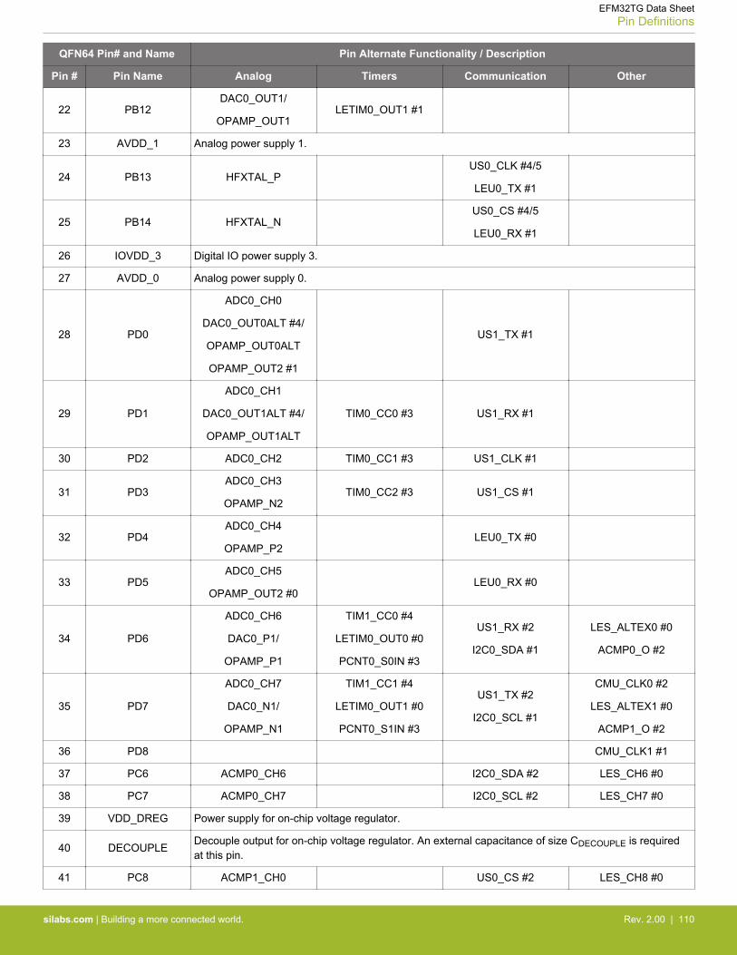
QFN64 Pin# and Name Pin Alternate Functionality / Description
Pin # Pin Name Analog Timers Communication Other
22 PB12DAC0_OUT1/
OPAMP_OUT1LETIM0_OUT1 #1
23 AVDD_1 Analog power supply 1.
24 PB13 HFXTAL_PUS0_CLK #4/5
LEU0_TX #1
25 PB14 HFXTAL_NUS0_CS #4/5
LEU0_RX #1
26 IOVDD_3 Digital IO power supply 3.
27 AVDD_0 Analog power supply 0.
28 PD0
ADC0_CH0
DAC0_OUT0ALT #4/
OPAMP_OUT0ALT
OPAMP_OUT2 #1
US1_TX #1
29 PD1
ADC0_CH1
DAC0_OUT1ALT #4/
OPAMP_OUT1ALT
TIM0_CC0 #3 US1_RX #1
30 PD2 ADC0_CH2 TIM0_CC1 #3 US1_CLK #1
31 PD3ADC0_CH3
OPAMP_N2TIM0_CC2 #3 US1_CS #1
32 PD4ADC0_CH4
OPAMP_P2LEU0_TX #0
33 PD5ADC0_CH5
OPAMP_OUT2 #0LEU0_RX #0
34 PD6
ADC0_CH6
DAC0_P1/
OPAMP_P1
TIM1_CC0 #4
LETIM0_OUT0 #0
PCNT0_S0IN #3
US1_RX #2
I2C0_SDA #1
LES_ALTEX0 #0
ACMP0_O #2
35 PD7
ADC0_CH7
DAC0_N1/
OPAMP_N1
TIM1_CC1 #4
LETIM0_OUT1 #0
PCNT0_S1IN #3
US1_TX #2
I2C0_SCL #1
CMU_CLK0 #2
LES_ALTEX1 #0
ACMP1_O #2
36 PD8 CMU_CLK1 #1
37 PC6 ACMP0_CH6 I2C0_SDA #2 LES_CH6 #0
38 PC7 ACMP0_CH7 I2C0_SCL #2 LES_CH7 #0
39 VDD_DREG Power supply for on-chip voltage regulator.
40 DECOUPLEDecouple output for on-chip voltage regulator. An external capacitance of size CDECOUPLE is requiredat this pin.
41 PC8 ACMP1_CH0 US0_CS #2 LES_CH8 #0
EFM32TG Data SheetPin Definitions
silabs.com | Building a more connected world. Rev. 2.00 | 110
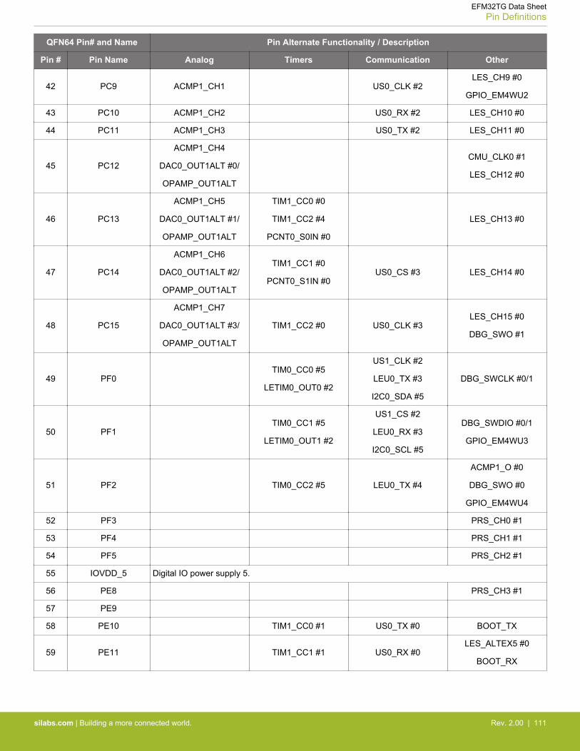
QFN64 Pin# and Name Pin Alternate Functionality / Description
Pin # Pin Name Analog Timers Communication Other
42 PC9 ACMP1_CH1 US0_CLK #2LES_CH9 #0
GPIO_EM4WU2
43 PC10 ACMP1_CH2 US0_RX #2 LES_CH10 #0
44 PC11 ACMP1_CH3 US0_TX #2 LES_CH11 #0
45 PC12
ACMP1_CH4
DAC0_OUT1ALT #0/
OPAMP_OUT1ALT
CMU_CLK0 #1
LES_CH12 #0
46 PC13
ACMP1_CH5
DAC0_OUT1ALT #1/
OPAMP_OUT1ALT
TIM1_CC0 #0
TIM1_CC2 #4
PCNT0_S0IN #0
LES_CH13 #0
47 PC14
ACMP1_CH6
DAC0_OUT1ALT #2/
OPAMP_OUT1ALT
TIM1_CC1 #0
PCNT0_S1IN #0US0_CS #3 LES_CH14 #0
48 PC15
ACMP1_CH7
DAC0_OUT1ALT #3/
OPAMP_OUT1ALT
TIM1_CC2 #0 US0_CLK #3LES_CH15 #0
DBG_SWO #1
49 PF0TIM0_CC0 #5
LETIM0_OUT0 #2
US1_CLK #2
LEU0_TX #3
I2C0_SDA #5
DBG_SWCLK #0/1
50 PF1TIM0_CC1 #5
LETIM0_OUT1 #2
US1_CS #2
LEU0_RX #3
I2C0_SCL #5
DBG_SWDIO #0/1
GPIO_EM4WU3
51 PF2 TIM0_CC2 #5 LEU0_TX #4
ACMP1_O #0
DBG_SWO #0
GPIO_EM4WU4
52 PF3 PRS_CH0 #1
53 PF4 PRS_CH1 #1
54 PF5 PRS_CH2 #1
55 IOVDD_5 Digital IO power supply 5.
56 PE8 PRS_CH3 #1
57 PE9
58 PE10 TIM1_CC0 #1 US0_TX #0 BOOT_TX
59 PE11 TIM1_CC1 #1 US0_RX #0LES_ALTEX5 #0
BOOT_RX
EFM32TG Data SheetPin Definitions
silabs.com | Building a more connected world. Rev. 2.00 | 111
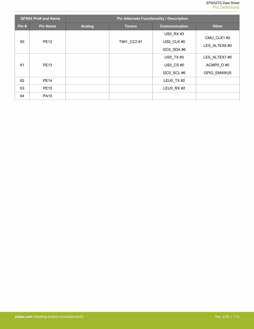
QFN64 Pin# and Name Pin Alternate Functionality / Description
Pin # Pin Name Analog Timers Communication Other
60 PE12 TIM1_CC2 #1
US0_RX #3
US0_CLK #0
I2C0_SDA #6
CMU_CLK1 #2
LES_ALTEX6 #0
61 PE13
US0_TX #3
US0_CS #0
I2C0_SCL #6
LES_ALTEX7 #0
ACMP0_O #0
GPIO_EM4WU5
62 PE14 LEU0_TX #2
63 PE15 LEU0_RX #2
64 PA15
EFM32TG Data SheetPin Definitions
silabs.com | Building a more connected world. Rev. 2.00 | 112
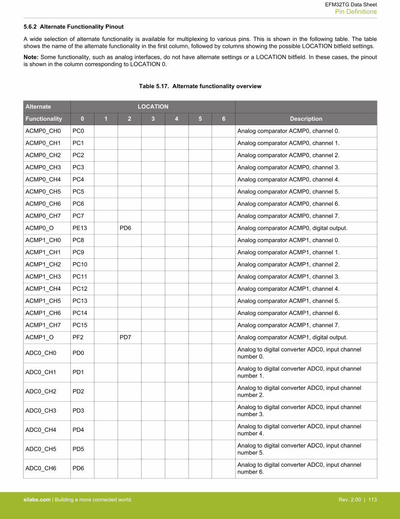
5.6.2 Alternate Functionality Pinout
A wide selection of alternate functionality is available for multiplexing to various pins. This is shown in the following table. The tableshows the name of the alternate functionality in the first column, followed by columns showing the possible LOCATION bitfield settings.
Note: Some functionality, such as analog interfaces, do not have alternate settings or a LOCATION bitfield. In these cases, the pinoutis shown in the column corresponding to LOCATION 0.
Table 5.17. Alternate functionality overview
Alternate LOCATION
Functionality 0 1 2 3 4 5 6 Description
ACMP0_CH0 PC0 Analog comparator ACMP0, channel 0.
ACMP0_CH1 PC1 Analog comparator ACMP0, channel 1.
ACMP0_CH2 PC2 Analog comparator ACMP0, channel 2.
ACMP0_CH3 PC3 Analog comparator ACMP0, channel 3.
ACMP0_CH4 PC4 Analog comparator ACMP0, channel 4.
ACMP0_CH5 PC5 Analog comparator ACMP0, channel 5.
ACMP0_CH6 PC6 Analog comparator ACMP0, channel 6.
ACMP0_CH7 PC7 Analog comparator ACMP0, channel 7.
ACMP0_O PE13 PD6 Analog comparator ACMP0, digital output.
ACMP1_CH0 PC8 Analog comparator ACMP1, channel 0.
ACMP1_CH1 PC9 Analog comparator ACMP1, channel 1.
ACMP1_CH2 PC10 Analog comparator ACMP1, channel 2.
ACMP1_CH3 PC11 Analog comparator ACMP1, channel 3.
ACMP1_CH4 PC12 Analog comparator ACMP1, channel 4.
ACMP1_CH5 PC13 Analog comparator ACMP1, channel 5.
ACMP1_CH6 PC14 Analog comparator ACMP1, channel 6.
ACMP1_CH7 PC15 Analog comparator ACMP1, channel 7.
ACMP1_O PF2 PD7 Analog comparator ACMP1, digital output.
ADC0_CH0 PD0 Analog to digital converter ADC0, input channelnumber 0.
ADC0_CH1 PD1 Analog to digital converter ADC0, input channelnumber 1.
ADC0_CH2 PD2 Analog to digital converter ADC0, input channelnumber 2.
ADC0_CH3 PD3 Analog to digital converter ADC0, input channelnumber 3.
ADC0_CH4 PD4 Analog to digital converter ADC0, input channelnumber 4.
ADC0_CH5 PD5 Analog to digital converter ADC0, input channelnumber 5.
ADC0_CH6 PD6 Analog to digital converter ADC0, input channelnumber 6.
EFM32TG Data SheetPin Definitions
silabs.com | Building a more connected world. Rev. 2.00 | 113
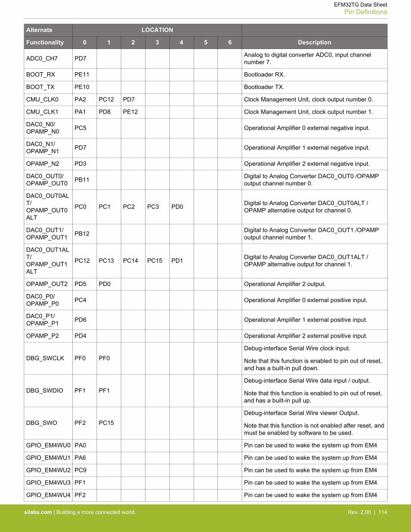
Alternate LOCATION
Functionality 0 1 2 3 4 5 6 Description
ADC0_CH7 PD7 Analog to digital converter ADC0, input channelnumber 7.
BOOT_RX PE11 Bootloader RX.
BOOT_TX PE10 Bootloader TX.
CMU_CLK0 PA2 PC12 PD7 Clock Management Unit, clock output number 0.
CMU_CLK1 PA1 PD8 PE12 Clock Management Unit, clock output number 1.
DAC0_N0/OPAMP_N0 PC5 Operational Amplifier 0 external negative input.
DAC0_N1/OPAMP_N1 PD7 Operational Amplifier 1 external negative input.
OPAMP_N2 PD3 Operational Amplifier 2 external negative input.
DAC0_OUT0/OPAMP_OUT0 PB11 Digital to Analog Converter DAC0_OUT0 /OPAMP
output channel number 0.
DAC0_OUT0ALT/OPAMP_OUT0ALT
PC0 PC1 PC2 PC3 PD0 Digital to Analog Converter DAC0_OUT0ALT /OPAMP alternative output for channel 0.
DAC0_OUT1/OPAMP_OUT1 PB12 Digital to Analog Converter DAC0_OUT1 /OPAMP
output channel number 1.
DAC0_OUT1ALT/OPAMP_OUT1ALT
PC12 PC13 PC14 PC15 PD1 Digital to Analog Converter DAC0_OUT1ALT /OPAMP alternative output for channel 1.
OPAMP_OUT2 PD5 PD0 Operational Amplifier 2 output.
DAC0_P0/OPAMP_P0 PC4 Operational Amplifier 0 external positive input.
DAC0_P1/OPAMP_P1 PD6 Operational Amplifier 1 external positive input.
OPAMP_P2 PD4 Operational Amplifier 2 external positive input.
DBG_SWCLK PF0 PF0Debug-interface Serial Wire clock input.
Note that this function is enabled to pin out of reset,and has a built-in pull down.
DBG_SWDIO PF1 PF1Debug-interface Serial Wire data input / output.
Note that this function is enabled to pin out of reset,and has a built-in pull up.
DBG_SWO PF2 PC15Debug-interface Serial Wire viewer Output.
Note that this function is not enabled after reset, andmust be enabled by software to be used.
GPIO_EM4WU0 PA0 Pin can be used to wake the system up from EM4
GPIO_EM4WU1 PA6 Pin can be used to wake the system up from EM4
GPIO_EM4WU2 PC9 Pin can be used to wake the system up from EM4
GPIO_EM4WU3 PF1 Pin can be used to wake the system up from EM4
GPIO_EM4WU4 PF2 Pin can be used to wake the system up from EM4
EFM32TG Data SheetPin Definitions
silabs.com | Building a more connected world. Rev. 2.00 | 114
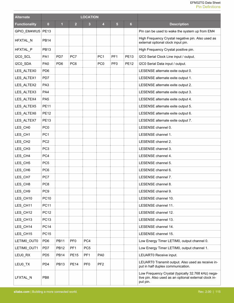
Alternate LOCATION
Functionality 0 1 2 3 4 5 6 Description
GPIO_EM4WU5 PE13 Pin can be used to wake the system up from EM4
HFXTAL_N PB14 High Frequency Crystal negative pin. Also used asexternal optional clock input pin.
HFXTAL_P PB13 High Frequency Crystal positive pin.
I2C0_SCL PA1 PD7 PC7 PC1 PF1 PE13 I2C0 Serial Clock Line input / output.
I2C0_SDA PA0 PD6 PC6 PC0 PF0 PE12 I2C0 Serial Data input / output.
LES_ALTEX0 PD6 LESENSE alternate exite output 0.
LES_ALTEX1 PD7 LESENSE alternate exite output 1.
LES_ALTEX2 PA3 LESENSE alternate exite output 2.
LES_ALTEX3 PA4 LESENSE alternate exite output 3.
LES_ALTEX4 PA5 LESENSE alternate exite output 4.
LES_ALTEX5 PE11 LESENSE alternate exite output 5.
LES_ALTEX6 PE12 LESENSE alternate exite output 6.
LES_ALTEX7 PE13 LESENSE alternate exite output 7.
LES_CH0 PC0 LESENSE channel 0.
LES_CH1 PC1 LESENSE channel 1.
LES_CH2 PC2 LESENSE channel 2.
LES_CH3 PC3 LESENSE channel 3.
LES_CH4 PC4 LESENSE channel 4.
LES_CH5 PC5 LESENSE channel 5.
LES_CH6 PC6 LESENSE channel 6.
LES_CH7 PC7 LESENSE channel 7.
LES_CH8 PC8 LESENSE channel 8.
LES_CH9 PC9 LESENSE channel 9.
LES_CH10 PC10 LESENSE channel 10.
LES_CH11 PC11 LESENSE channel 11.
LES_CH12 PC12 LESENSE channel 12.
LES_CH13 PC13 LESENSE channel 13.
LES_CH14 PC14 LESENSE channel 14.
LES_CH15 PC15 LESENSE channel 15.
LETIM0_OUT0 PD6 PB11 PF0 PC4 Low Energy Timer LETIM0, output channel 0.
LETIM0_OUT1 PD7 PB12 PF1 PC5 Low Energy Timer LETIM0, output channel 1.
LEU0_RX PD5 PB14 PE15 PF1 PA0 LEUART0 Receive input.
LEU0_TX PD4 PB13 PE14 PF0 PF2 LEUART0 Transmit output. Also used as receive in-put in half duplex communication.
LFXTAL_N PB8Low Frequency Crystal (typically 32.768 kHz) nega-tive pin. Also used as an optional external clock in-put pin.
EFM32TG Data SheetPin Definitions
silabs.com | Building a more connected world. Rev. 2.00 | 115
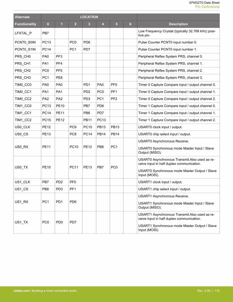
Alternate LOCATION
Functionality 0 1 2 3 4 5 6 Description
LFXTAL_P PB7 Low Frequency Crystal (typically 32.768 kHz) posi-tive pin.
PCNT0_S0IN PC13 PC0 PD6 Pulse Counter PCNT0 input number 0.
PCNT0_S1IN PC14 PC1 PD7 Pulse Counter PCNT0 input number 1.
PRS_CH0 PA0 PF3 Peripheral Reflex System PRS, channel 0.
PRS_CH1 PA1 PF4 Peripheral Reflex System PRS, channel 1.
PRS_CH2 PC0 PF5 Peripheral Reflex System PRS, channel 2.
PRS_CH3 PC1 PE8 Peripheral Reflex System PRS, channel 3.
TIM0_CC0 PA0 PA0 PD1 PA0 PF0 Timer 0 Capture Compare input / output channel 0.
TIM0_CC1 PA1 PA1 PD2 PC0 PF1 Timer 0 Capture Compare input / output channel 1.
TIM0_CC2 PA2 PA2 PD3 PC1 PF2 Timer 0 Capture Compare input / output channel 2.
TIM1_CC0 PC13 PE10 PB7 PD6 Timer 1 Capture Compare input / output channel 0.
TIM1_CC1 PC14 PE11 PB8 PD7 Timer 1 Capture Compare input / output channel 1.
TIM1_CC2 PC15 PE12 PB11 PC13 Timer 1 Capture Compare input / output channel 2.
US0_CLK PE12 PC9 PC15 PB13 PB13 USART0 clock input / output.
US0_CS PE13 PC8 PC14 PB14 PB14 USART0 chip select input / output.
US0_RX PE11 PC10 PE12 PB8 PC1USART0 Asynchronous Receive.
USART0 Synchronous mode Master Input / SlaveOutput (MISO).
US0_TX PE10 PC11 PE13 PB7 PC0
USART0 Asynchronous Transmit.Also used as re-ceive input in half duplex communication.
USART0 Synchronous mode Master Output / SlaveInput (MOSI).
US1_CLK PB7 PD2 PF0 USART1 clock input / output.
US1_CS PB8 PD3 PF1 USART1 chip select input / output.
US1_RX PC1 PD1 PD6USART1 Asynchronous Receive.
USART1 Synchronous mode Master Input / SlaveOutput (MISO).
US1_TX PC0 PD0 PD7
USART1 Asynchronous Transmit.Also used as re-ceive input in half duplex communication.
USART1 Synchronous mode Master Output / SlaveInput (MOSI).
EFM32TG Data SheetPin Definitions
silabs.com | Building a more connected world. Rev. 2.00 | 116
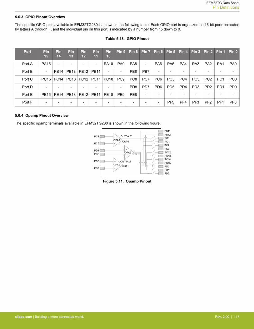
5.6.3 GPIO Pinout Overview
The specific GPIO pins available in EFM32TG230 is shown in the following table. Each GPIO port is organized as 16-bit ports indicatedby letters A through F, and the individual pin on this port is indicated by a number from 15 down to 0.
Table 5.18. GPIO Pinout
Port Pin15
Pin14
Pin13
Pin12
Pin11
Pin10
Pin 9 Pin 8 Pin 7 Pin 6 Pin 5 Pin 4 Pin 3 Pin 2 Pin 1 Pin 0
Port A PA15 - - - - PA10 PA9 PA8 - PA6 PA5 PA4 PA3 PA2 PA1 PA0
Port B - PB14 PB13 PB12 PB11 - - PB8 PB7 - - - - - - -
Port C PC15 PC14 PC13 PC12 PC11 PC10 PC9 PC8 PC7 PC6 PC5 PC4 PC3 PC2 PC1 PC0
Port D - - - - - - - PD8 PD7 PD6 PD5 PD4 PD3 PD2 PD1 PD0
Port E PE15 PE14 PE13 PE12 PE11 PE10 PE9 PE8 - - - - - - - -
Port F - - - - - - - - - - PF5 PF4 PF3 PF2 PF1 PF0
5.6.4 Opamp Pinout Overview
The specific opamp terminals available in EFM32TG230 is shown in the following figure.
-
+OPA0
-
+OPA2
-
+OPA1
OUT0ALT
OUT0
OUT2
OUT1ALT
OUT1
PC4
PC5
PD4PD3
PD6
PD7
PB11PB12PC0PC1PC2PC3PC12PC13PC14PC15PD0PD1PD5
Figure 5.11. Opamp Pinout
EFM32TG Data SheetPin Definitions
silabs.com | Building a more connected world. Rev. 2.00 | 117
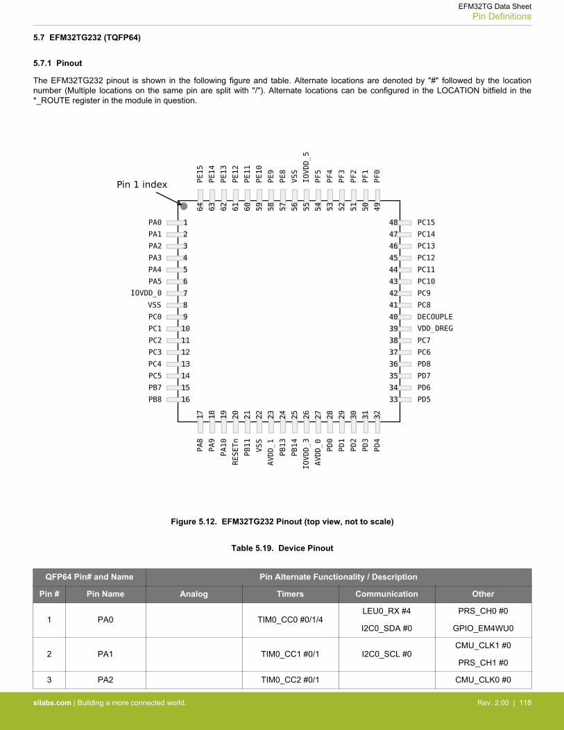
5.7 EFM32TG232 (TQFP64)
5.7.1 Pinout
The EFM32TG232 pinout is shown in the following figure and table. Alternate locations are denoted by "#" followed by the locationnumber (Multiple locations on the same pin are split with "/"). Alternate locations can be configured in the LOCATION bitfield in the*_ROUTE register in the module in question.
Figure 5.12. EFM32TG232 Pinout (top view, not to scale)
Table 5.19. Device Pinout
QFP64 Pin# and Name Pin Alternate Functionality / Description
Pin # Pin Name Analog Timers Communication Other
1 PA0 TIM0_CC0 #0/1/4LEU0_RX #4
I2C0_SDA #0
PRS_CH0 #0
GPIO_EM4WU0
2 PA1 TIM0_CC1 #0/1 I2C0_SCL #0CMU_CLK1 #0
PRS_CH1 #0
3 PA2 TIM0_CC2 #0/1 CMU_CLK0 #0
EFM32TG Data SheetPin Definitions
silabs.com | Building a more connected world. Rev. 2.00 | 118
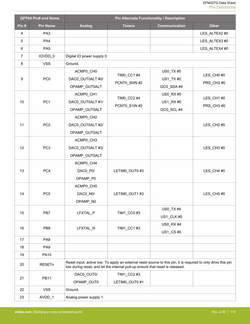
QFP64 Pin# and Name Pin Alternate Functionality / Description
Pin # Pin Name Analog Timers Communication Other
4 PA3 LES_ALTEX2 #0
5 PA4 LES_ALTEX3 #0
6 PA5 LES_ALTEX4 #0
7 IOVDD_0 Digital IO power supply 0.
8 VSS Ground.
9 PC0
ACMP0_CH0
DAC0_OUT0ALT #0/
OPAMP_OUT0ALT
TIM0_CC1 #4
PCNT0_S0IN #2
US0_TX #5
US1_TX #0
I2C0_SDA #4
LES_CH0 #0
PRS_CH2 #0
10 PC1
ACMP0_CH1
DAC0_OUT0ALT #1/
OPAMP_OUT0ALT
TIM0_CC2 #4
PCNT0_S1IN #2
US0_RX #5
US1_RX #0
I2C0_SCL #4
LES_CH1 #0
PRS_CH3 #0
11 PC2
ACMP0_CH2
DAC0_OUT0ALT #2/
OPAMP_OUT0ALT
LES_CH2 #0
12 PC3
ACMP0_CH3
DAC0_OUT0ALT #3/
OPAMP_OUT0ALT
LES_CH3 #0
13 PC4
ACMP0_CH4
DAC0_P0/
OPAMP_P0
LETIM0_OUT0 #3 LES_CH4 #0
14 PC5
ACMP0_CH5
DAC0_N0/
OPAMP_N0
LETIM0_OUT1 #3 LES_CH5 #0
15 PB7 LFXTAL_P TIM1_CC0 #3US0_TX #4
US1_CLK #0
16 PB8 LFXTAL_N TIM1_CC1 #3US0_RX #4
US1_CS #0
17 PA8
18 PA9
19 PA10
20 RESETn Reset input, active low. To apply an external reset source to this pin, it is required to only drive this pinlow during reset, and let the internal pull-up ensure that reset is released.
21 PB11DAC0_OUT0/
OPAMP_OUT0
TIM1_CC2 #3
LETIM0_OUT0 #1
22 VSS Ground.
23 AVDD_1 Analog power supply 1.
EFM32TG Data SheetPin Definitions
silabs.com | Building a more connected world. Rev. 2.00 | 119
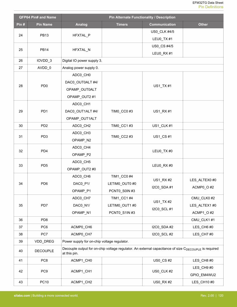
QFP64 Pin# and Name Pin Alternate Functionality / Description
Pin # Pin Name Analog Timers Communication Other
24 PB13 HFXTAL_PUS0_CLK #4/5
LEU0_TX #1
25 PB14 HFXTAL_NUS0_CS #4/5
LEU0_RX #1
26 IOVDD_3 Digital IO power supply 3.
27 AVDD_0 Analog power supply 0.
28 PD0
ADC0_CH0
DAC0_OUT0ALT #4/
OPAMP_OUT0ALT
OPAMP_OUT2 #1
US1_TX #1
29 PD1
ADC0_CH1
DAC0_OUT1ALT #4/
OPAMP_OUT1ALT
TIM0_CC0 #3 US1_RX #1
30 PD2 ADC0_CH2 TIM0_CC1 #3 US1_CLK #1
31 PD3ADC0_CH3
OPAMP_N2TIM0_CC2 #3 US1_CS #1
32 PD4ADC0_CH4
OPAMP_P2LEU0_TX #0
33 PD5ADC0_CH5
OPAMP_OUT2 #0LEU0_RX #0
34 PD6
ADC0_CH6
DAC0_P1/
OPAMP_P1
TIM1_CC0 #4
LETIM0_OUT0 #0
PCNT0_S0IN #3
US1_RX #2
I2C0_SDA #1
LES_ALTEX0 #0
ACMP0_O #2
35 PD7
ADC0_CH7
DAC0_N1/
OPAMP_N1
TIM1_CC1 #4
LETIM0_OUT1 #0
PCNT0_S1IN #3
US1_TX #2
I2C0_SCL #1
CMU_CLK0 #2
LES_ALTEX1 #0
ACMP1_O #2
36 PD8 CMU_CLK1 #1
37 PC6 ACMP0_CH6 I2C0_SDA #2 LES_CH6 #0
38 PC7 ACMP0_CH7 I2C0_SCL #2 LES_CH7 #0
39 VDD_DREG Power supply for on-chip voltage regulator.
40 DECOUPLEDecouple output for on-chip voltage regulator. An external capacitance of size CDECOUPLE is requiredat this pin.
41 PC8 ACMP1_CH0 US0_CS #2 LES_CH8 #0
42 PC9 ACMP1_CH1 US0_CLK #2LES_CH9 #0
GPIO_EM4WU2
43 PC10 ACMP1_CH2 US0_RX #2 LES_CH10 #0
EFM32TG Data SheetPin Definitions
silabs.com | Building a more connected world. Rev. 2.00 | 120
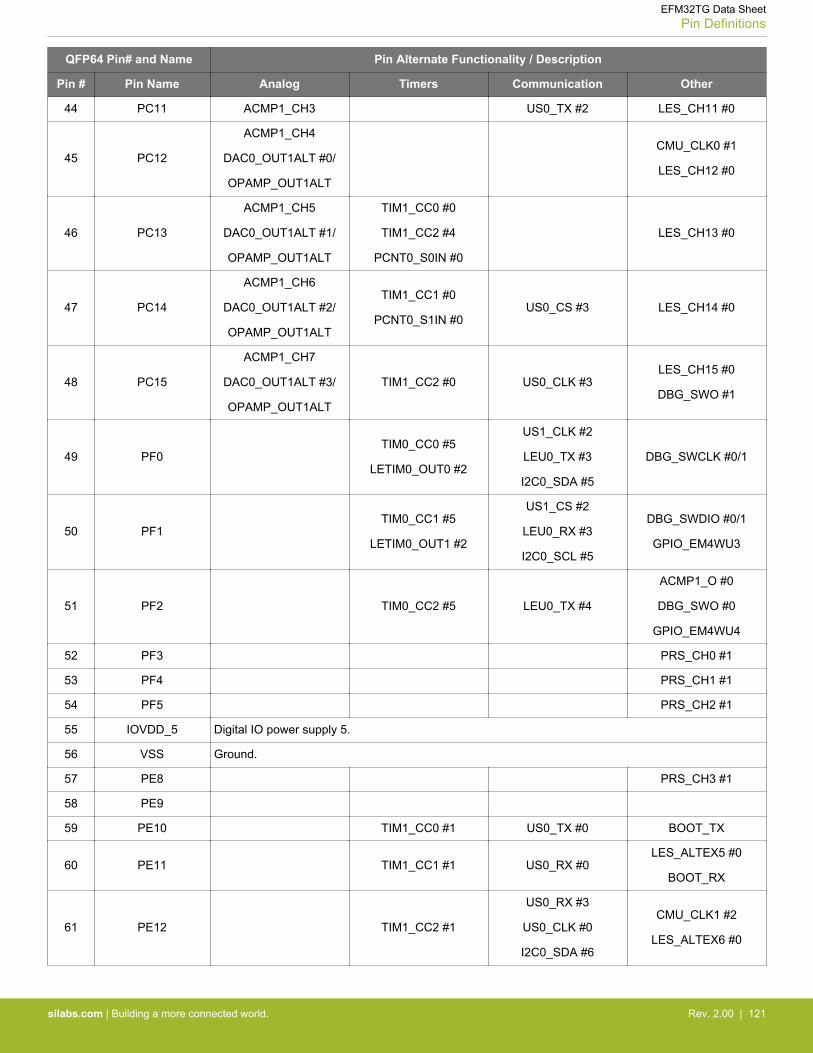
QFP64 Pin# and Name Pin Alternate Functionality / Description
Pin # Pin Name Analog Timers Communication Other
44 PC11 ACMP1_CH3 US0_TX #2 LES_CH11 #0
45 PC12
ACMP1_CH4
DAC0_OUT1ALT #0/
OPAMP_OUT1ALT
CMU_CLK0 #1
LES_CH12 #0
46 PC13
ACMP1_CH5
DAC0_OUT1ALT #1/
OPAMP_OUT1ALT
TIM1_CC0 #0
TIM1_CC2 #4
PCNT0_S0IN #0
LES_CH13 #0
47 PC14
ACMP1_CH6
DAC0_OUT1ALT #2/
OPAMP_OUT1ALT
TIM1_CC1 #0
PCNT0_S1IN #0US0_CS #3 LES_CH14 #0
48 PC15
ACMP1_CH7
DAC0_OUT1ALT #3/
OPAMP_OUT1ALT
TIM1_CC2 #0 US0_CLK #3LES_CH15 #0
DBG_SWO #1
49 PF0TIM0_CC0 #5
LETIM0_OUT0 #2
US1_CLK #2
LEU0_TX #3
I2C0_SDA #5
DBG_SWCLK #0/1
50 PF1TIM0_CC1 #5
LETIM0_OUT1 #2
US1_CS #2
LEU0_RX #3
I2C0_SCL #5
DBG_SWDIO #0/1
GPIO_EM4WU3
51 PF2 TIM0_CC2 #5 LEU0_TX #4
ACMP1_O #0
DBG_SWO #0
GPIO_EM4WU4
52 PF3 PRS_CH0 #1
53 PF4 PRS_CH1 #1
54 PF5 PRS_CH2 #1
55 IOVDD_5 Digital IO power supply 5.
56 VSS Ground.
57 PE8 PRS_CH3 #1
58 PE9
59 PE10 TIM1_CC0 #1 US0_TX #0 BOOT_TX
60 PE11 TIM1_CC1 #1 US0_RX #0LES_ALTEX5 #0
BOOT_RX
61 PE12 TIM1_CC2 #1
US0_RX #3
US0_CLK #0
I2C0_SDA #6
CMU_CLK1 #2
LES_ALTEX6 #0
EFM32TG Data SheetPin Definitions
silabs.com | Building a more connected world. Rev. 2.00 | 121
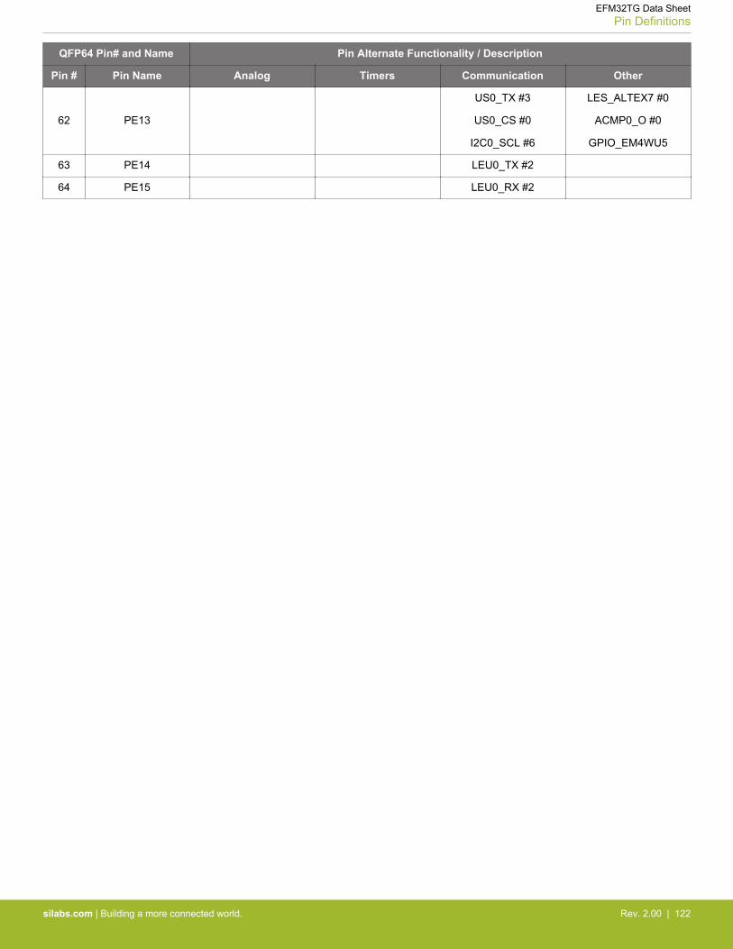
QFP64 Pin# and Name Pin Alternate Functionality / Description
Pin # Pin Name Analog Timers Communication Other
62 PE13
US0_TX #3
US0_CS #0
I2C0_SCL #6
LES_ALTEX7 #0
ACMP0_O #0
GPIO_EM4WU5
63 PE14 LEU0_TX #2
64 PE15 LEU0_RX #2
EFM32TG Data SheetPin Definitions
silabs.com | Building a more connected world. Rev. 2.00 | 122

5.7.2 Alternate Functionality Pinout
A wide selection of alternate functionality is available for multiplexing to various pins. This is shown in the following table. The tableshows the name of the alternate functionality in the first column, followed by columns showing the possible LOCATION bitfield settings.
Note: Some functionality, such as analog interfaces, do not have alternate settings or a LOCATION bitfield. In these cases, the pinoutis shown in the column corresponding to LOCATION 0.
Table 5.20. Alternate functionality overview
Alternate LOCATION
Functionality 0 1 2 3 4 5 6 Description
ACMP0_CH0 PC0 Analog comparator ACMP0, channel 0.
ACMP0_CH1 PC1 Analog comparator ACMP0, channel 1.
ACMP0_CH2 PC2 Analog comparator ACMP0, channel 2.
ACMP0_CH3 PC3 Analog comparator ACMP0, channel 3.
ACMP0_CH4 PC4 Analog comparator ACMP0, channel 4.
ACMP0_CH5 PC5 Analog comparator ACMP0, channel 5.
ACMP0_CH6 PC6 Analog comparator ACMP0, channel 6.
ACMP0_CH7 PC7 Analog comparator ACMP0, channel 7.
ACMP0_O PE13 PD6 Analog comparator ACMP0, digital output.
ACMP1_CH0 PC8 Analog comparator ACMP1, channel 0.
ACMP1_CH1 PC9 Analog comparator ACMP1, channel 1.
ACMP1_CH2 PC10 Analog comparator ACMP1, channel 2.
ACMP1_CH3 PC11 Analog comparator ACMP1, channel 3.
ACMP1_CH4 PC12 Analog comparator ACMP1, channel 4.
ACMP1_CH5 PC13 Analog comparator ACMP1, channel 5.
ACMP1_CH6 PC14 Analog comparator ACMP1, channel 6.
ACMP1_CH7 PC15 Analog comparator ACMP1, channel 7.
ACMP1_O PF2 PD7 Analog comparator ACMP1, digital output.
ADC0_CH0 PD0 Analog to digital converter ADC0, input channelnumber 0.
ADC0_CH1 PD1 Analog to digital converter ADC0, input channelnumber 1.
ADC0_CH2 PD2 Analog to digital converter ADC0, input channelnumber 2.
ADC0_CH3 PD3 Analog to digital converter ADC0, input channelnumber 3.
ADC0_CH4 PD4 Analog to digital converter ADC0, input channelnumber 4.
ADC0_CH5 PD5 Analog to digital converter ADC0, input channelnumber 5.
ADC0_CH6 PD6 Analog to digital converter ADC0, input channelnumber 6.
EFM32TG Data SheetPin Definitions
silabs.com | Building a more connected world. Rev. 2.00 | 123
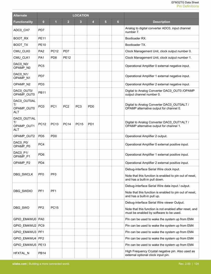
Alternate LOCATION
Functionality 0 1 2 3 4 5 6 Description
ADC0_CH7 PD7 Analog to digital converter ADC0, input channelnumber 7.
BOOT_RX PE11 Bootloader RX.
BOOT_TX PE10 Bootloader TX.
CMU_CLK0 PA2 PC12 PD7 Clock Management Unit, clock output number 0.
CMU_CLK1 PA1 PD8 PE12 Clock Management Unit, clock output number 1.
DAC0_N0/OPAMP_N0 PC5 Operational Amplifier 0 external negative input.
DAC0_N1/OPAMP_N1 PD7 Operational Amplifier 1 external negative input.
OPAMP_N2 PD3 Operational Amplifier 2 external negative input.
DAC0_OUT0/OPAMP_OUT0 PB11 Digital to Analog Converter DAC0_OUT0 /OPAMP
output channel number 0.
DAC0_OUT0ALT/OPAMP_OUT0ALT
PC0 PC1 PC2 PC3 PD0 Digital to Analog Converter DAC0_OUT0ALT /OPAMP alternative output for channel 0.
DAC0_OUT1ALT/OPAMP_OUT1ALT
PC12 PC13 PC14 PC15 PD1 Digital to Analog Converter DAC0_OUT1ALT /OPAMP alternative output for channel 1.
OPAMP_OUT2 PD5 PD0 Operational Amplifier 2 output.
DAC0_P0/OPAMP_P0 PC4 Operational Amplifier 0 external positive input.
DAC0_P1/OPAMP_P1 PD6 Operational Amplifier 1 external positive input.
OPAMP_P2 PD4 Operational Amplifier 2 external positive input.
DBG_SWCLK PF0 PF0Debug-interface Serial Wire clock input.
Note that this function is enabled to pin out of reset,and has a built-in pull down.
DBG_SWDIO PF1 PF1Debug-interface Serial Wire data input / output.
Note that this function is enabled to pin out of reset,and has a built-in pull up.
DBG_SWO PF2 PC15Debug-interface Serial Wire viewer Output.
Note that this function is not enabled after reset, andmust be enabled by software to be used.
GPIO_EM4WU0 PA0 Pin can be used to wake the system up from EM4
GPIO_EM4WU2 PC9 Pin can be used to wake the system up from EM4
GPIO_EM4WU3 PF1 Pin can be used to wake the system up from EM4
GPIO_EM4WU4 PF2 Pin can be used to wake the system up from EM4
GPIO_EM4WU5 PE13 Pin can be used to wake the system up from EM4
HFXTAL_N PB14 High Frequency Crystal negative pin. Also used asexternal optional clock input pin.
EFM32TG Data SheetPin Definitions
silabs.com | Building a more connected world. Rev. 2.00 | 124
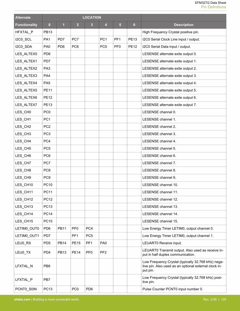
Alternate LOCATION
Functionality 0 1 2 3 4 5 6 Description
HFXTAL_P PB13 High Frequency Crystal positive pin.
I2C0_SCL PA1 PD7 PC7 PC1 PF1 PE13 I2C0 Serial Clock Line input / output.
I2C0_SDA PA0 PD6 PC6 PC0 PF0 PE12 I2C0 Serial Data input / output.
LES_ALTEX0 PD6 LESENSE alternate exite output 0.
LES_ALTEX1 PD7 LESENSE alternate exite output 1.
LES_ALTEX2 PA3 LESENSE alternate exite output 2.
LES_ALTEX3 PA4 LESENSE alternate exite output 3.
LES_ALTEX4 PA5 LESENSE alternate exite output 4.
LES_ALTEX5 PE11 LESENSE alternate exite output 5.
LES_ALTEX6 PE12 LESENSE alternate exite output 6.
LES_ALTEX7 PE13 LESENSE alternate exite output 7.
LES_CH0 PC0 LESENSE channel 0.
LES_CH1 PC1 LESENSE channel 1.
LES_CH2 PC2 LESENSE channel 2.
LES_CH3 PC3 LESENSE channel 3.
LES_CH4 PC4 LESENSE channel 4.
LES_CH5 PC5 LESENSE channel 5.
LES_CH6 PC6 LESENSE channel 6.
LES_CH7 PC7 LESENSE channel 7.
LES_CH8 PC8 LESENSE channel 8.
LES_CH9 PC9 LESENSE channel 9.
LES_CH10 PC10 LESENSE channel 10.
LES_CH11 PC11 LESENSE channel 11.
LES_CH12 PC12 LESENSE channel 12.
LES_CH13 PC13 LESENSE channel 13.
LES_CH14 PC14 LESENSE channel 14.
LES_CH15 PC15 LESENSE channel 15.
LETIM0_OUT0 PD6 PB11 PF0 PC4 Low Energy Timer LETIM0, output channel 0.
LETIM0_OUT1 PD7 PF1 PC5 Low Energy Timer LETIM0, output channel 1.
LEU0_RX PD5 PB14 PE15 PF1 PA0 LEUART0 Receive input.
LEU0_TX PD4 PB13 PE14 PF0 PF2 LEUART0 Transmit output. Also used as receive in-put in half duplex communication.
LFXTAL_N PB8Low Frequency Crystal (typically 32.768 kHz) nega-tive pin. Also used as an optional external clock in-put pin.
LFXTAL_P PB7 Low Frequency Crystal (typically 32.768 kHz) posi-tive pin.
PCNT0_S0IN PC13 PC0 PD6 Pulse Counter PCNT0 input number 0.
EFM32TG Data SheetPin Definitions
silabs.com | Building a more connected world. Rev. 2.00 | 125

Alternate LOCATION
Functionality 0 1 2 3 4 5 6 Description
PCNT0_S1IN PC14 PC1 PD7 Pulse Counter PCNT0 input number 1.
PRS_CH0 PA0 PF3 Peripheral Reflex System PRS, channel 0.
PRS_CH1 PA1 PF4 Peripheral Reflex System PRS, channel 1.
PRS_CH2 PC0 PF5 Peripheral Reflex System PRS, channel 2.
PRS_CH3 PC1 PE8 Peripheral Reflex System PRS, channel 3.
TIM0_CC0 PA0 PA0 PD1 PA0 PF0 Timer 0 Capture Compare input / output channel 0.
TIM0_CC1 PA1 PA1 PD2 PC0 PF1 Timer 0 Capture Compare input / output channel 1.
TIM0_CC2 PA2 PA2 PD3 PC1 PF2 Timer 0 Capture Compare input / output channel 2.
TIM1_CC0 PC13 PE10 PB7 PD6 Timer 1 Capture Compare input / output channel 0.
TIM1_CC1 PC14 PE11 PB8 PD7 Timer 1 Capture Compare input / output channel 1.
TIM1_CC2 PC15 PE12 PB11 PC13 Timer 1 Capture Compare input / output channel 2.
US0_CLK PE12 PC9 PC15 PB13 PB13 USART0 clock input / output.
US0_CS PE13 PC8 PC14 PB14 PB14 USART0 chip select input / output.
US0_RX PE11 PC10 PE12 PB8 PC1USART0 Asynchronous Receive.
USART0 Synchronous mode Master Input / SlaveOutput (MISO).
US0_TX PE10 PC11 PE13 PB7 PC0
USART0 Asynchronous Transmit.Also used as re-ceive input in half duplex communication.
USART0 Synchronous mode Master Output / SlaveInput (MOSI).
US1_CLK PB7 PD2 PF0 USART1 clock input / output.
US1_CS PB8 PD3 PF1 USART1 chip select input / output.
US1_RX PC1 PD1 PD6USART1 Asynchronous Receive.
USART1 Synchronous mode Master Input / SlaveOutput (MISO).
US1_TX PC0 PD0 PD7
USART1 Asynchronous Transmit.Also used as re-ceive input in half duplex communication.
USART1 Synchronous mode Master Output / SlaveInput (MOSI).
EFM32TG Data SheetPin Definitions
silabs.com | Building a more connected world. Rev. 2.00 | 126
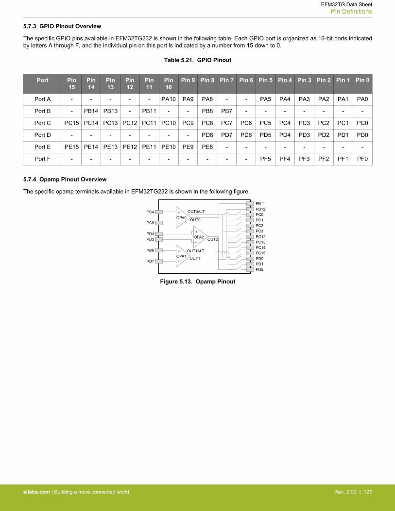
5.7.3 GPIO Pinout Overview
The specific GPIO pins available in EFM32TG232 is shown in the following table. Each GPIO port is organized as 16-bit ports indicatedby letters A through F, and the individual pin on this port is indicated by a number from 15 down to 0.
Table 5.21. GPIO Pinout
Port Pin15
Pin14
Pin13
Pin12
Pin11
Pin10
Pin 9 Pin 8 Pin 7 Pin 6 Pin 5 Pin 4 Pin 3 Pin 2 Pin 1 Pin 0
Port A - - - - - PA10 PA9 PA8 - - PA5 PA4 PA3 PA2 PA1 PA0
Port B - PB14 PB13 - PB11 - - PB8 PB7 - - - - - - -
Port C PC15 PC14 PC13 PC12 PC11 PC10 PC9 PC8 PC7 PC6 PC5 PC4 PC3 PC2 PC1 PC0
Port D - - - - - - - PD8 PD7 PD6 PD5 PD4 PD3 PD2 PD1 PD0
Port E PE15 PE14 PE13 PE12 PE11 PE10 PE9 PE8 - - - - - - - -
Port F - - - - - - - - - - PF5 PF4 PF3 PF2 PF1 PF0
5.7.4 Opamp Pinout Overview
The specific opamp terminals available in EFM32TG232 is shown in the following figure.
-
+OPA0
-
+OPA2
-
+OPA1
OUT0ALT
OUT0
OUT2
OUT1ALT
OUT1
PC4
PC5
PD4PD3
PD6
PD7
PB11PB12PC0PC1PC2PC3PC12PC13PC14PC15PD0PD1PD5
Figure 5.13. Opamp Pinout
EFM32TG Data SheetPin Definitions
silabs.com | Building a more connected world. Rev. 2.00 | 127

5.8 EFM32TG822 (TQFP48)
5.8.1 Pinout
The EFM32TG822 pinout is shown in the following figure and table. Alternate locations are denoted by "#" followed by the locationnumber (Multiple locations on the same pin are split with "/"). Alternate locations can be configured in the LOCATION bitfield in the*_ROUTE register in the module in question.
Figure 5.14. EFM32TG822 Pinout (top view, not to scale)
Table 5.22. Device Pinout
QFP48 Pin# and Name Pin Alternate Functionality / Description
Pin # Pin Name Analog Timers Communication Other
1 PA0 LCD_SEG13 TIM0_CC0 #0/1/4LEU0_RX #4
I2C0_SDA #0
PRS_CH0 #0
GPIO_EM4WU0
2 PA1 LCD_SEG14 TIM0_CC1 #0/1 I2C0_SCL #0CMU_CLK1 #0
PRS_CH1 #0
3 PA2 LCD_SEG15 TIM0_CC2 #0/1 CMU_CLK0 #0
EFM32TG Data SheetPin Definitions
silabs.com | Building a more connected world. Rev. 2.00 | 128
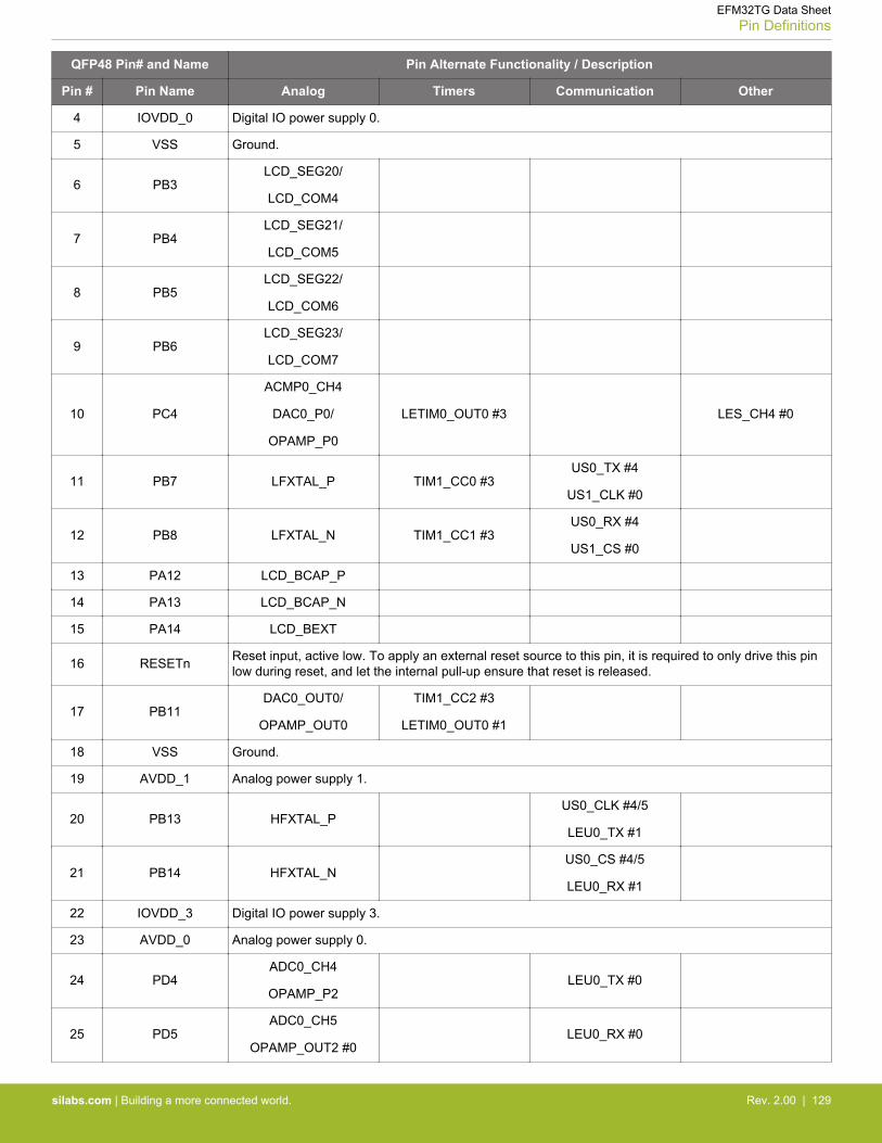
QFP48 Pin# and Name Pin Alternate Functionality / Description
Pin # Pin Name Analog Timers Communication Other
4 IOVDD_0 Digital IO power supply 0.
5 VSS Ground.
6 PB3LCD_SEG20/
LCD_COM4
7 PB4LCD_SEG21/
LCD_COM5
8 PB5LCD_SEG22/
LCD_COM6
9 PB6LCD_SEG23/
LCD_COM7
10 PC4
ACMP0_CH4
DAC0_P0/
OPAMP_P0
LETIM0_OUT0 #3 LES_CH4 #0
11 PB7 LFXTAL_P TIM1_CC0 #3US0_TX #4
US1_CLK #0
12 PB8 LFXTAL_N TIM1_CC1 #3US0_RX #4
US1_CS #0
13 PA12 LCD_BCAP_P
14 PA13 LCD_BCAP_N
15 PA14 LCD_BEXT
16 RESETn Reset input, active low. To apply an external reset source to this pin, it is required to only drive this pinlow during reset, and let the internal pull-up ensure that reset is released.
17 PB11DAC0_OUT0/
OPAMP_OUT0
TIM1_CC2 #3
LETIM0_OUT0 #1
18 VSS Ground.
19 AVDD_1 Analog power supply 1.
20 PB13 HFXTAL_PUS0_CLK #4/5
LEU0_TX #1
21 PB14 HFXTAL_NUS0_CS #4/5
LEU0_RX #1
22 IOVDD_3 Digital IO power supply 3.
23 AVDD_0 Analog power supply 0.
24 PD4ADC0_CH4
OPAMP_P2LEU0_TX #0
25 PD5ADC0_CH5
OPAMP_OUT2 #0LEU0_RX #0
EFM32TG Data SheetPin Definitions
silabs.com | Building a more connected world. Rev. 2.00 | 129
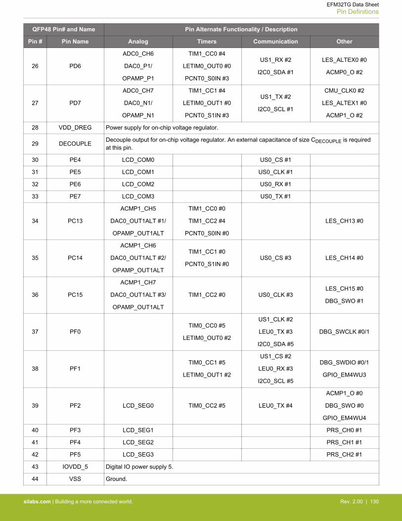
QFP48 Pin# and Name Pin Alternate Functionality / Description
Pin # Pin Name Analog Timers Communication Other
26 PD6
ADC0_CH6
DAC0_P1/
OPAMP_P1
TIM1_CC0 #4
LETIM0_OUT0 #0
PCNT0_S0IN #3
US1_RX #2
I2C0_SDA #1
LES_ALTEX0 #0
ACMP0_O #2
27 PD7
ADC0_CH7
DAC0_N1/
OPAMP_N1
TIM1_CC1 #4
LETIM0_OUT1 #0
PCNT0_S1IN #3
US1_TX #2
I2C0_SCL #1
CMU_CLK0 #2
LES_ALTEX1 #0
ACMP1_O #2
28 VDD_DREG Power supply for on-chip voltage regulator.
29 DECOUPLEDecouple output for on-chip voltage regulator. An external capacitance of size CDECOUPLE is requiredat this pin.
30 PE4 LCD_COM0 US0_CS #1
31 PE5 LCD_COM1 US0_CLK #1
32 PE6 LCD_COM2 US0_RX #1
33 PE7 LCD_COM3 US0_TX #1
34 PC13
ACMP1_CH5
DAC0_OUT1ALT #1/
OPAMP_OUT1ALT
TIM1_CC0 #0
TIM1_CC2 #4
PCNT0_S0IN #0
LES_CH13 #0
35 PC14
ACMP1_CH6
DAC0_OUT1ALT #2/
OPAMP_OUT1ALT
TIM1_CC1 #0
PCNT0_S1IN #0US0_CS #3 LES_CH14 #0
36 PC15
ACMP1_CH7
DAC0_OUT1ALT #3/
OPAMP_OUT1ALT
TIM1_CC2 #0 US0_CLK #3LES_CH15 #0
DBG_SWO #1
37 PF0TIM0_CC0 #5
LETIM0_OUT0 #2
US1_CLK #2
LEU0_TX #3
I2C0_SDA #5
DBG_SWCLK #0/1
38 PF1TIM0_CC1 #5
LETIM0_OUT1 #2
US1_CS #2
LEU0_RX #3
I2C0_SCL #5
DBG_SWDIO #0/1
GPIO_EM4WU3
39 PF2 LCD_SEG0 TIM0_CC2 #5 LEU0_TX #4
ACMP1_O #0
DBG_SWO #0
GPIO_EM4WU4
40 PF3 LCD_SEG1 PRS_CH0 #1
41 PF4 LCD_SEG2 PRS_CH1 #1
42 PF5 LCD_SEG3 PRS_CH2 #1
43 IOVDD_5 Digital IO power supply 5.
44 VSS Ground.
EFM32TG Data SheetPin Definitions
silabs.com | Building a more connected world. Rev. 2.00 | 130
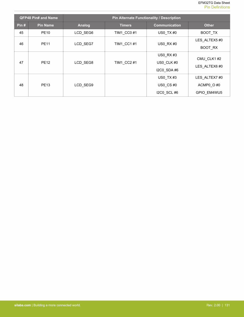
QFP48 Pin# and Name Pin Alternate Functionality / Description
Pin # Pin Name Analog Timers Communication Other
45 PE10 LCD_SEG6 TIM1_CC0 #1 US0_TX #0 BOOT_TX
46 PE11 LCD_SEG7 TIM1_CC1 #1 US0_RX #0LES_ALTEX5 #0
BOOT_RX
47 PE12 LCD_SEG8 TIM1_CC2 #1
US0_RX #3
US0_CLK #0
I2C0_SDA #6
CMU_CLK1 #2
LES_ALTEX6 #0
48 PE13 LCD_SEG9
US0_TX #3
US0_CS #0
I2C0_SCL #6
LES_ALTEX7 #0
ACMP0_O #0
GPIO_EM4WU5
EFM32TG Data SheetPin Definitions
silabs.com | Building a more connected world. Rev. 2.00 | 131

5.8.2 Alternate Functionality Pinout
A wide selection of alternate functionality is available for multiplexing to various pins. This is shown in the following table. The tableshows the name of the alternate functionality in the first column, followed by columns showing the possible LOCATION bitfield settings.
Note: Some functionality, such as analog interfaces, do not have alternate settings or a LOCATION bitfield. In these cases, the pinoutis shown in the column corresponding to LOCATION 0.
Table 5.23. Alternate functionality overview
Alternate LOCATION
Functionality 0 1 2 3 4 5 6 Description
ACMP0_CH4 PC4 Analog comparator ACMP0, channel 4.
ACMP0_O PE13 PD6 Analog comparator ACMP0, digital output.
ACMP1_CH5 PC13 Analog comparator ACMP1, channel 5.
ACMP1_CH6 PC14 Analog comparator ACMP1, channel 6.
ACMP1_CH7 PC15 Analog comparator ACMP1, channel 7.
ACMP1_O PF2 PD7 Analog comparator ACMP1, digital output.
ADC0_CH4 PD4 Analog to digital converter ADC0, input channelnumber 4.
ADC0_CH5 PD5 Analog to digital converter ADC0, input channelnumber 5.
ADC0_CH6 PD6 Analog to digital converter ADC0, input channelnumber 6.
ADC0_CH7 PD7 Analog to digital converter ADC0, input channelnumber 7.
BOOT_RX PE11 Bootloader RX.
BOOT_TX PE10 Bootloader TX.
CMU_CLK0 PA2 PD7 Clock Management Unit, clock output number 0.
CMU_CLK1 PA1 PE12 Clock Management Unit, clock output number 1.
DAC0_N1/OPAMP_N1 PD7 Operational Amplifier 1 external negative input.
DAC0_OUT0/OPAMP_OUT0 PB11 Digital to Analog Converter DAC0_OUT0 /OPAMP
output channel number 0.
DAC0_OUT1ALT/OPAMP_OUT1ALT
PC13 PC14 PC15 Digital to Analog Converter DAC0_OUT1ALT /OPAMP alternative output for channel 1.
OPAMP_OUT2 PD5 Operational Amplifier 2 output.
DAC0_P0/OPAMP_P0 PC4 Operational Amplifier 0 external positive input.
DAC0_P1/OPAMP_P1 PD6 Operational Amplifier 1 external positive input.
OPAMP_P2 PD4 Operational Amplifier 2 external positive input.
DBG_SWCLK PF0 PF0Debug-interface Serial Wire clock input.
Note that this function is enabled to pin out of reset,and has a built-in pull down.
EFM32TG Data SheetPin Definitions
silabs.com | Building a more connected world. Rev. 2.00 | 132

Alternate LOCATION
Functionality 0 1 2 3 4 5 6 Description
DBG_SWDIO PF1 PF1Debug-interface Serial Wire data input / output.
Note that this function is enabled to pin out of reset,and has a built-in pull up.
DBG_SWO PF2 PC15Debug-interface Serial Wire viewer Output.
Note that this function is not enabled after reset, andmust be enabled by software to be used.
GPIO_EM4WU0 PA0 Pin can be used to wake the system up from EM4
GPIO_EM4WU3 PF1 Pin can be used to wake the system up from EM4
GPIO_EM4WU4 PF2 Pin can be used to wake the system up from EM4
GPIO_EM4WU5 PE13 Pin can be used to wake the system up from EM4
HFXTAL_N PB14 High Frequency Crystal negative pin. Also used asexternal optional clock input pin.
HFXTAL_P PB13 High Frequency Crystal positive pin.
I2C0_SCL PA1 PD7 PF1 PE13 I2C0 Serial Clock Line input / output.
I2C0_SDA PA0 PD6 PF0 PE12 I2C0 Serial Data input / output.
LCD_BCAP_N PA13
LCD voltage booster (optional), boost capacitor,negative pin. If using the LCD voltage booster, con-nect a 22 nF capacitor between LCD_BCAP_N andLCD_BCAP_P.
LCD_BCAP_P PA12
LCD voltage booster (optional), boost capacitor,positive pin. If using the LCD voltage booster, con-nect a 22 nF capacitor between LCD_BCAP_N andLCD_BCAP_P.
LCD_BEXT PA14
LCD voltage booster (optional), boost output. If us-ing the LCD voltage booster, connect a 1 uF capaci-tor between this pin and VSS.
An external LCD voltage may also be applied to thispin if the booster is not enabled.
If AVDD is used directly as the LCD supply voltage,this pin may be left unconnected or used as a GPIO.
LCD_COM0 PE4 LCD driver common line number 0.
LCD_COM1 PE5 LCD driver common line number 1.
LCD_COM2 PE6 LCD driver common line number 2.
LCD_COM3 PE7 LCD driver common line number 3.
LCD_SEG0 PF2 LCD segment line 0. Segments 0, 1, 2 and 3 arecontrolled by SEGEN0.
LCD_SEG1 PF3 LCD segment line 1. Segments 0, 1, 2 and 3 arecontrolled by SEGEN0.
LCD_SEG2 PF4 LCD segment line 2. Segments 0, 1, 2 and 3 arecontrolled by SEGEN0.
LCD_SEG3 PF5 LCD segment line 3. Segments 0, 1, 2 and 3 arecontrolled by SEGEN0.
EFM32TG Data SheetPin Definitions
silabs.com | Building a more connected world. Rev. 2.00 | 133
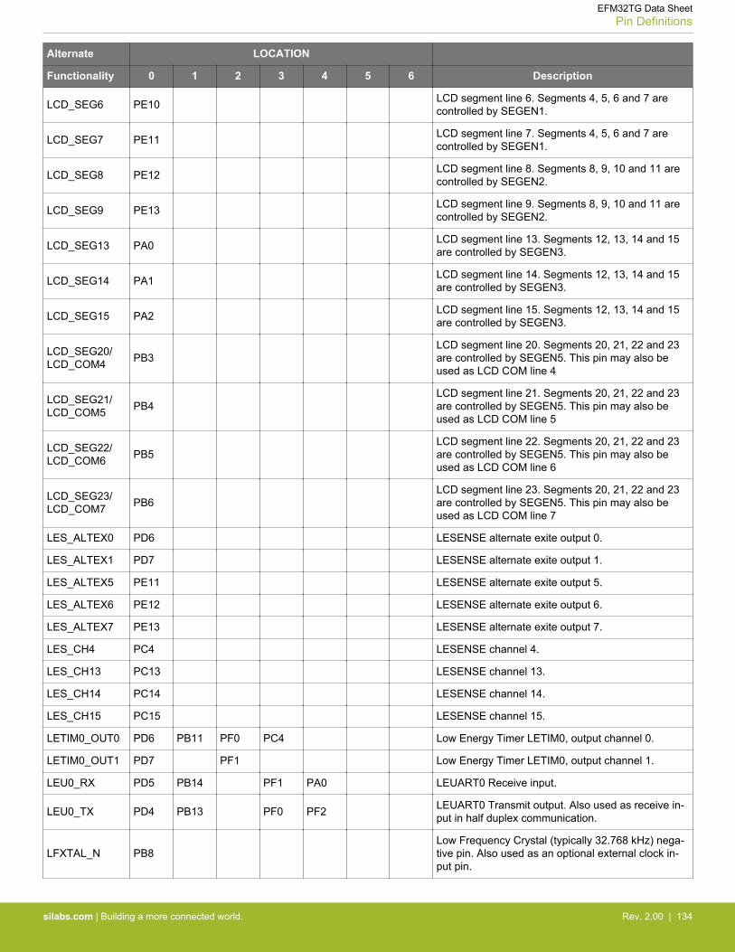
Alternate LOCATION
Functionality 0 1 2 3 4 5 6 Description
LCD_SEG6 PE10 LCD segment line 6. Segments 4, 5, 6 and 7 arecontrolled by SEGEN1.
LCD_SEG7 PE11 LCD segment line 7. Segments 4, 5, 6 and 7 arecontrolled by SEGEN1.
LCD_SEG8 PE12 LCD segment line 8. Segments 8, 9, 10 and 11 arecontrolled by SEGEN2.
LCD_SEG9 PE13 LCD segment line 9. Segments 8, 9, 10 and 11 arecontrolled by SEGEN2.
LCD_SEG13 PA0 LCD segment line 13. Segments 12, 13, 14 and 15are controlled by SEGEN3.
LCD_SEG14 PA1 LCD segment line 14. Segments 12, 13, 14 and 15are controlled by SEGEN3.
LCD_SEG15 PA2 LCD segment line 15. Segments 12, 13, 14 and 15are controlled by SEGEN3.
LCD_SEG20/LCD_COM4 PB3
LCD segment line 20. Segments 20, 21, 22 and 23are controlled by SEGEN5. This pin may also beused as LCD COM line 4
LCD_SEG21/LCD_COM5 PB4
LCD segment line 21. Segments 20, 21, 22 and 23are controlled by SEGEN5. This pin may also beused as LCD COM line 5
LCD_SEG22/LCD_COM6 PB5
LCD segment line 22. Segments 20, 21, 22 and 23are controlled by SEGEN5. This pin may also beused as LCD COM line 6
LCD_SEG23/LCD_COM7 PB6
LCD segment line 23. Segments 20, 21, 22 and 23are controlled by SEGEN5. This pin may also beused as LCD COM line 7
LES_ALTEX0 PD6 LESENSE alternate exite output 0.
LES_ALTEX1 PD7 LESENSE alternate exite output 1.
LES_ALTEX5 PE11 LESENSE alternate exite output 5.
LES_ALTEX6 PE12 LESENSE alternate exite output 6.
LES_ALTEX7 PE13 LESENSE alternate exite output 7.
LES_CH4 PC4 LESENSE channel 4.
LES_CH13 PC13 LESENSE channel 13.
LES_CH14 PC14 LESENSE channel 14.
LES_CH15 PC15 LESENSE channel 15.
LETIM0_OUT0 PD6 PB11 PF0 PC4 Low Energy Timer LETIM0, output channel 0.
LETIM0_OUT1 PD7 PF1 Low Energy Timer LETIM0, output channel 1.
LEU0_RX PD5 PB14 PF1 PA0 LEUART0 Receive input.
LEU0_TX PD4 PB13 PF0 PF2 LEUART0 Transmit output. Also used as receive in-put in half duplex communication.
LFXTAL_N PB8Low Frequency Crystal (typically 32.768 kHz) nega-tive pin. Also used as an optional external clock in-put pin.
EFM32TG Data SheetPin Definitions
silabs.com | Building a more connected world. Rev. 2.00 | 134

Alternate LOCATION
Functionality 0 1 2 3 4 5 6 Description
LFXTAL_P PB7 Low Frequency Crystal (typically 32.768 kHz) posi-tive pin.
PCNT0_S0IN PC13 PD6 Pulse Counter PCNT0 input number 0.
PCNT0_S1IN PC14 PD7 Pulse Counter PCNT0 input number 1.
PRS_CH0 PA0 PF3 Peripheral Reflex System PRS, channel 0.
PRS_CH1 PA1 PF4 Peripheral Reflex System PRS, channel 1.
PRS_CH2 PF5 Peripheral Reflex System PRS, channel 2.
TIM0_CC0 PA0 PA0 PA0 PF0 Timer 0 Capture Compare input / output channel 0.
TIM0_CC1 PA1 PA1 PF1 Timer 0 Capture Compare input / output channel 1.
TIM0_CC2 PA2 PA2 PF2 Timer 0 Capture Compare input / output channel 2.
TIM1_CC0 PC13 PE10 PB7 PD6 Timer 1 Capture Compare input / output channel 0.
TIM1_CC1 PC14 PE11 PB8 PD7 Timer 1 Capture Compare input / output channel 1.
TIM1_CC2 PC15 PE12 PB11 PC13 Timer 1 Capture Compare input / output channel 2.
US0_CLK PE12 PE5 PC15 PB13 PB13 USART0 clock input / output.
US0_CS PE13 PE4 PC14 PB14 PB14 USART0 chip select input / output.
US0_RX PE11 PE6 PE12 PB8USART0 Asynchronous Receive.
USART0 Synchronous mode Master Input / SlaveOutput (MISO).
US0_TX PE10 PE7 PE13 PB7
USART0 Asynchronous Transmit.Also used as re-ceive input in half duplex communication.
USART0 Synchronous mode Master Output / SlaveInput (MOSI).
US1_CLK PB7 PF0 USART1 clock input / output.
US1_CS PB8 PF1 USART1 chip select input / output.
US1_RX PD6USART1 Asynchronous Receive.
USART1 Synchronous mode Master Input / SlaveOutput (MISO).
US1_TX PD7
USART1 Asynchronous Transmit.Also used as re-ceive input in half duplex communication.
USART1 Synchronous mode Master Output / SlaveInput (MOSI).
EFM32TG Data SheetPin Definitions
silabs.com | Building a more connected world. Rev. 2.00 | 135
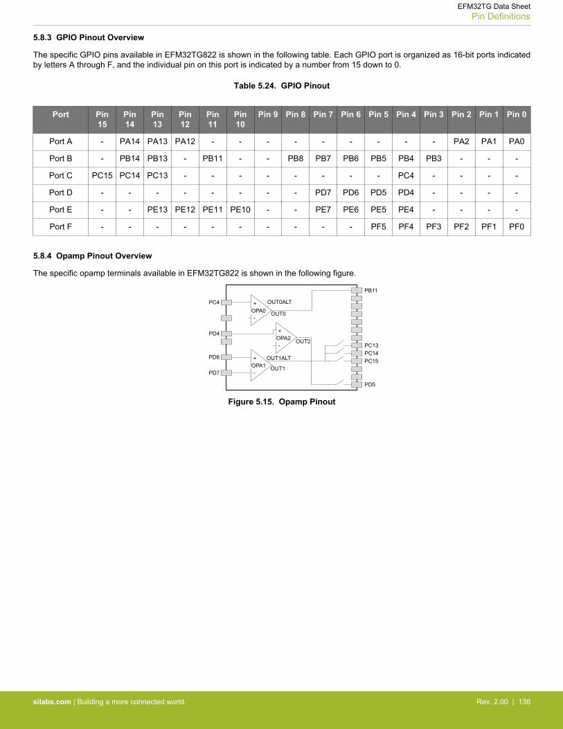
5.8.3 GPIO Pinout Overview
The specific GPIO pins available in EFM32TG822 is shown in the following table. Each GPIO port is organized as 16-bit ports indicatedby letters A through F, and the individual pin on this port is indicated by a number from 15 down to 0.
Table 5.24. GPIO Pinout
Port Pin15
Pin14
Pin13
Pin12
Pin11
Pin10
Pin 9 Pin 8 Pin 7 Pin 6 Pin 5 Pin 4 Pin 3 Pin 2 Pin 1 Pin 0
Port A - PA14 PA13 PA12 - - - - - - - - - PA2 PA1 PA0
Port B - PB14 PB13 - PB11 - - PB8 PB7 PB6 PB5 PB4 PB3 - - -
Port C PC15 PC14 PC13 - - - - - - - - PC4 - - - -
Port D - - - - - - - - PD7 PD6 PD5 PD4 - - - -
Port E - - PE13 PE12 PE11 PE10 - - PE7 PE6 PE5 PE4 - - - -
Port F - - - - - - - - - - PF5 PF4 PF3 PF2 PF1 PF0
5.8.4 Opamp Pinout Overview
The specific opamp terminals available in EFM32TG822 is shown in the following figure.
-
+OPA0
-
+OPA2
-
+OPA1
OUT0ALT
OUT0
OUT2
OUT1ALT
OUT1
PC4
PD4
PD6
PD7
PB11
PC13PC14PC15
PD5
Figure 5.15. Opamp Pinout
EFM32TG Data SheetPin Definitions
silabs.com | Building a more connected world. Rev. 2.00 | 136
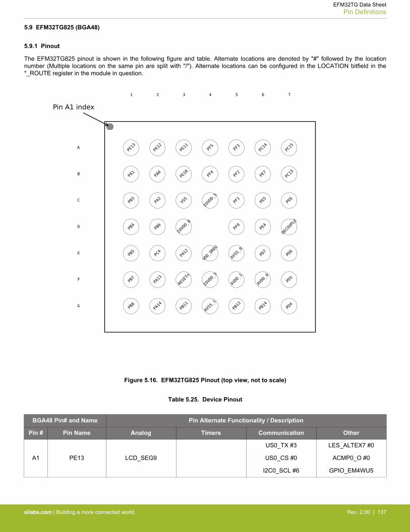
5.9 EFM32TG825 (BGA48)
5.9.1 Pinout
The EFM32TG825 pinout is shown in the following figure and table. Alternate locations are denoted by "#" followed by the locationnumber (Multiple locations on the same pin are split with "/"). Alternate locations can be configured in the LOCATION bitfield in the*_ROUTE register in the module in question.
Figure 5.16. EFM32TG825 Pinout (top view, not to scale)
Table 5.25. Device Pinout
BGA48 Pin# and Name Pin Alternate Functionality / Description
Pin # Pin Name Analog Timers Communication Other
A1 PE13 LCD_SEG9
US0_TX #3
US0_CS #0
I2C0_SCL #6
LES_ALTEX7 #0
ACMP0_O #0
GPIO_EM4WU5
EFM32TG Data SheetPin Definitions
silabs.com | Building a more connected world. Rev. 2.00 | 137
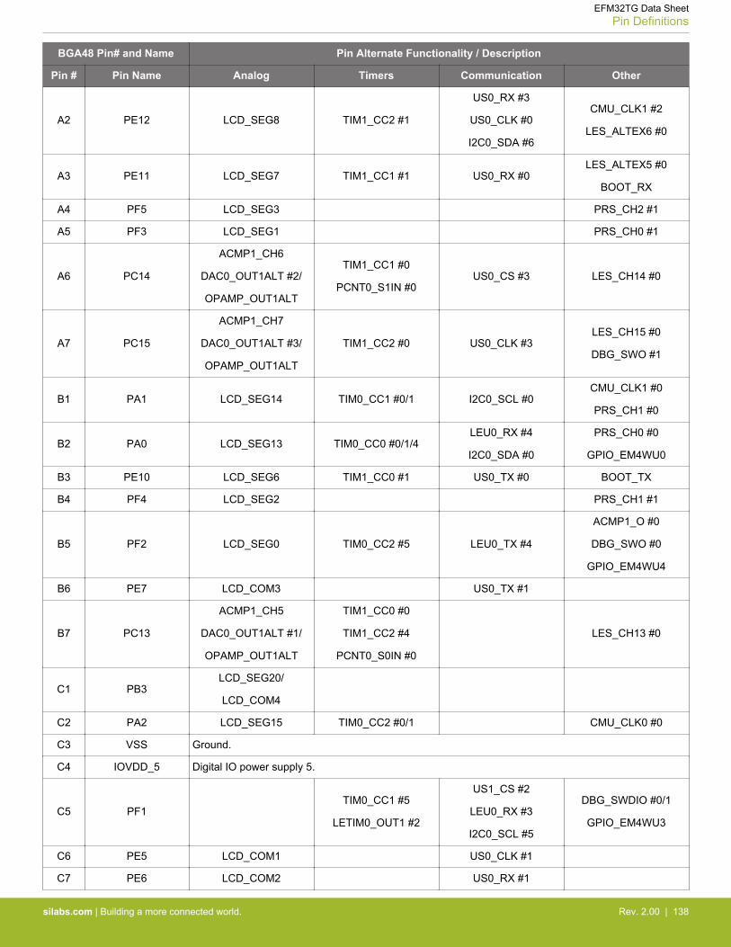
BGA48 Pin# and Name Pin Alternate Functionality / Description
Pin # Pin Name Analog Timers Communication Other
A2 PE12 LCD_SEG8 TIM1_CC2 #1
US0_RX #3
US0_CLK #0
I2C0_SDA #6
CMU_CLK1 #2
LES_ALTEX6 #0
A3 PE11 LCD_SEG7 TIM1_CC1 #1 US0_RX #0LES_ALTEX5 #0
BOOT_RX
A4 PF5 LCD_SEG3 PRS_CH2 #1
A5 PF3 LCD_SEG1 PRS_CH0 #1
A6 PC14
ACMP1_CH6
DAC0_OUT1ALT #2/
OPAMP_OUT1ALT
TIM1_CC1 #0
PCNT0_S1IN #0US0_CS #3 LES_CH14 #0
A7 PC15
ACMP1_CH7
DAC0_OUT1ALT #3/
OPAMP_OUT1ALT
TIM1_CC2 #0 US0_CLK #3LES_CH15 #0
DBG_SWO #1
B1 PA1 LCD_SEG14 TIM0_CC1 #0/1 I2C0_SCL #0CMU_CLK1 #0
PRS_CH1 #0
B2 PA0 LCD_SEG13 TIM0_CC0 #0/1/4LEU0_RX #4
I2C0_SDA #0
PRS_CH0 #0
GPIO_EM4WU0
B3 PE10 LCD_SEG6 TIM1_CC0 #1 US0_TX #0 BOOT_TX
B4 PF4 LCD_SEG2 PRS_CH1 #1
B5 PF2 LCD_SEG0 TIM0_CC2 #5 LEU0_TX #4
ACMP1_O #0
DBG_SWO #0
GPIO_EM4WU4
B6 PE7 LCD_COM3 US0_TX #1
B7 PC13
ACMP1_CH5
DAC0_OUT1ALT #1/
OPAMP_OUT1ALT
TIM1_CC0 #0
TIM1_CC2 #4
PCNT0_S0IN #0
LES_CH13 #0
C1 PB3LCD_SEG20/
LCD_COM4
C2 PA2 LCD_SEG15 TIM0_CC2 #0/1 CMU_CLK0 #0
C3 VSS Ground.
C4 IOVDD_5 Digital IO power supply 5.
C5 PF1TIM0_CC1 #5
LETIM0_OUT1 #2
US1_CS #2
LEU0_RX #3
I2C0_SCL #5
DBG_SWDIO #0/1
GPIO_EM4WU3
C6 PE5 LCD_COM1 US0_CLK #1
C7 PE6 LCD_COM2 US0_RX #1
EFM32TG Data SheetPin Definitions
silabs.com | Building a more connected world. Rev. 2.00 | 138
BGA48 Pin# and Name Pin Alternate Functionality / Description
Pin # Pin Name Analog Timers Communication Other
D1 PB4LCD_SEG21/
LCD_COM5
D2 PB6LCD_SEG23/
LCD_COM7
D3 IOVDD_0 Digital IO power supply 0.
D5 PF0TIM0_CC0 #5
LETIM0_OUT0 #2
US1_CLK #2
LEU0_TX #3
I2C0_SDA #5
DBG_SWCLK #0/1
D6 PE4 LCD_COM0 US0_CS #1
D7 DECOUPLEDecouple output for on-chip voltage regulator. An external capacitance of size CDECOUPLE is requiredat this pin.
E1 PB5LCD_SEG22/
LCD_COM6
E2 PC4
ACMP0_CH4
DAC0_P0/
OPAMP_P0
LETIM0_OUT0 #3 LES_CH4 #0
E3 PA12 LCD_BCAP_P
E4 VDD_DREG Power supply for on-chip voltage regulator.
E5 AVSS_0 Analog ground 0.
E6 PD7
ADC0_CH7
DAC0_N1/
OPAMP_N1
TIM1_CC1 #4
LETIM0_OUT1 #0
PCNT0_S1IN #3
US1_TX #2
I2C0_SCL #1
CMU_CLK0 #2
LES_ALTEX1 #0
ACMP1_O #2
E7 PD6
ADC0_CH6
DAC0_P1/
OPAMP_P1
TIM1_CC0 #4
LETIM0_OUT0 #0
PCNT0_S0IN #3
US1_RX #2
I2C0_SDA #1
LES_ALTEX0 #0
ACMP0_O #2
F1 PB7 LFXTAL_P TIM1_CC0 #3US0_TX #4
US1_CLK #0
F2 PA13 LCD_BCAP_N
F3 RESETn Reset input, active low. To apply an external reset source to this pin, it is required to only drive this pinlow during reset, and let the internal pull-up ensure that reset is released.
F4 IOVDD_3 Digital IO power supply 3.
F5 AVDD_1 Analog power supply 1.
F6 AVDD_0 Analog power supply 0.
F7 PD5ADC0_CH5
OPAMP_OUT2 #0LEU0_RX #0
G1 PB8 LFXTAL_N TIM1_CC1 #3US0_RX #4
US1_CS #0
EFM32TG Data SheetPin Definitions
silabs.com | Building a more connected world. Rev. 2.00 | 139
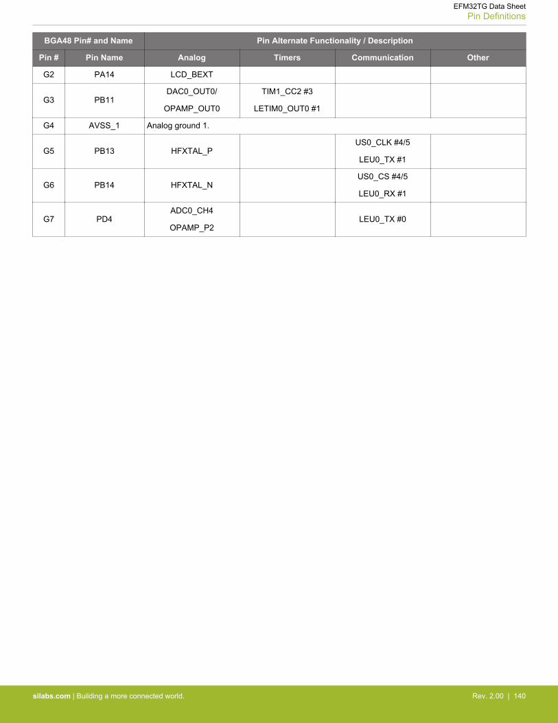
BGA48 Pin# and Name Pin Alternate Functionality / Description
Pin # Pin Name Analog Timers Communication Other
G2 PA14 LCD_BEXT
G3 PB11DAC0_OUT0/
OPAMP_OUT0
TIM1_CC2 #3
LETIM0_OUT0 #1
G4 AVSS_1 Analog ground 1.
G5 PB13 HFXTAL_PUS0_CLK #4/5
LEU0_TX #1
G6 PB14 HFXTAL_NUS0_CS #4/5
LEU0_RX #1
G7 PD4ADC0_CH4
OPAMP_P2LEU0_TX #0
EFM32TG Data SheetPin Definitions
silabs.com | Building a more connected world. Rev. 2.00 | 140
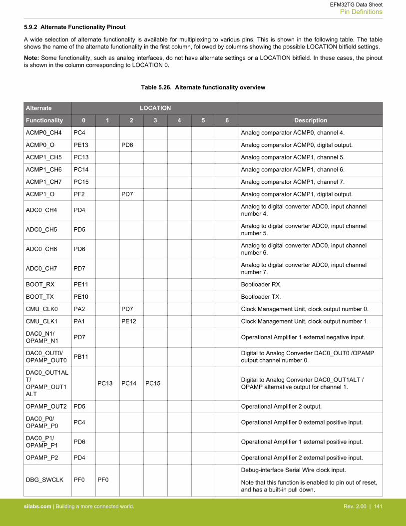
5.9.2 Alternate Functionality Pinout
A wide selection of alternate functionality is available for multiplexing to various pins. This is shown in the following table. The tableshows the name of the alternate functionality in the first column, followed by columns showing the possible LOCATION bitfield settings.
Note: Some functionality, such as analog interfaces, do not have alternate settings or a LOCATION bitfield. In these cases, the pinoutis shown in the column corresponding to LOCATION 0.
Table 5.26. Alternate functionality overview
Alternate LOCATION
Functionality 0 1 2 3 4 5 6 Description
ACMP0_CH4 PC4 Analog comparator ACMP0, channel 4.
ACMP0_O PE13 PD6 Analog comparator ACMP0, digital output.
ACMP1_CH5 PC13 Analog comparator ACMP1, channel 5.
ACMP1_CH6 PC14 Analog comparator ACMP1, channel 6.
ACMP1_CH7 PC15 Analog comparator ACMP1, channel 7.
ACMP1_O PF2 PD7 Analog comparator ACMP1, digital output.
ADC0_CH4 PD4 Analog to digital converter ADC0, input channelnumber 4.
ADC0_CH5 PD5 Analog to digital converter ADC0, input channelnumber 5.
ADC0_CH6 PD6 Analog to digital converter ADC0, input channelnumber 6.
ADC0_CH7 PD7 Analog to digital converter ADC0, input channelnumber 7.
BOOT_RX PE11 Bootloader RX.
BOOT_TX PE10 Bootloader TX.
CMU_CLK0 PA2 PD7 Clock Management Unit, clock output number 0.
CMU_CLK1 PA1 PE12 Clock Management Unit, clock output number 1.
DAC0_N1/OPAMP_N1 PD7 Operational Amplifier 1 external negative input.
DAC0_OUT0/OPAMP_OUT0 PB11 Digital to Analog Converter DAC0_OUT0 /OPAMP
output channel number 0.
DAC0_OUT1ALT/OPAMP_OUT1ALT
PC13 PC14 PC15 Digital to Analog Converter DAC0_OUT1ALT /OPAMP alternative output for channel 1.
OPAMP_OUT2 PD5 Operational Amplifier 2 output.
DAC0_P0/OPAMP_P0 PC4 Operational Amplifier 0 external positive input.
DAC0_P1/OPAMP_P1 PD6 Operational Amplifier 1 external positive input.
OPAMP_P2 PD4 Operational Amplifier 2 external positive input.
DBG_SWCLK PF0 PF0Debug-interface Serial Wire clock input.
Note that this function is enabled to pin out of reset,and has a built-in pull down.
EFM32TG Data SheetPin Definitions
silabs.com | Building a more connected world. Rev. 2.00 | 141
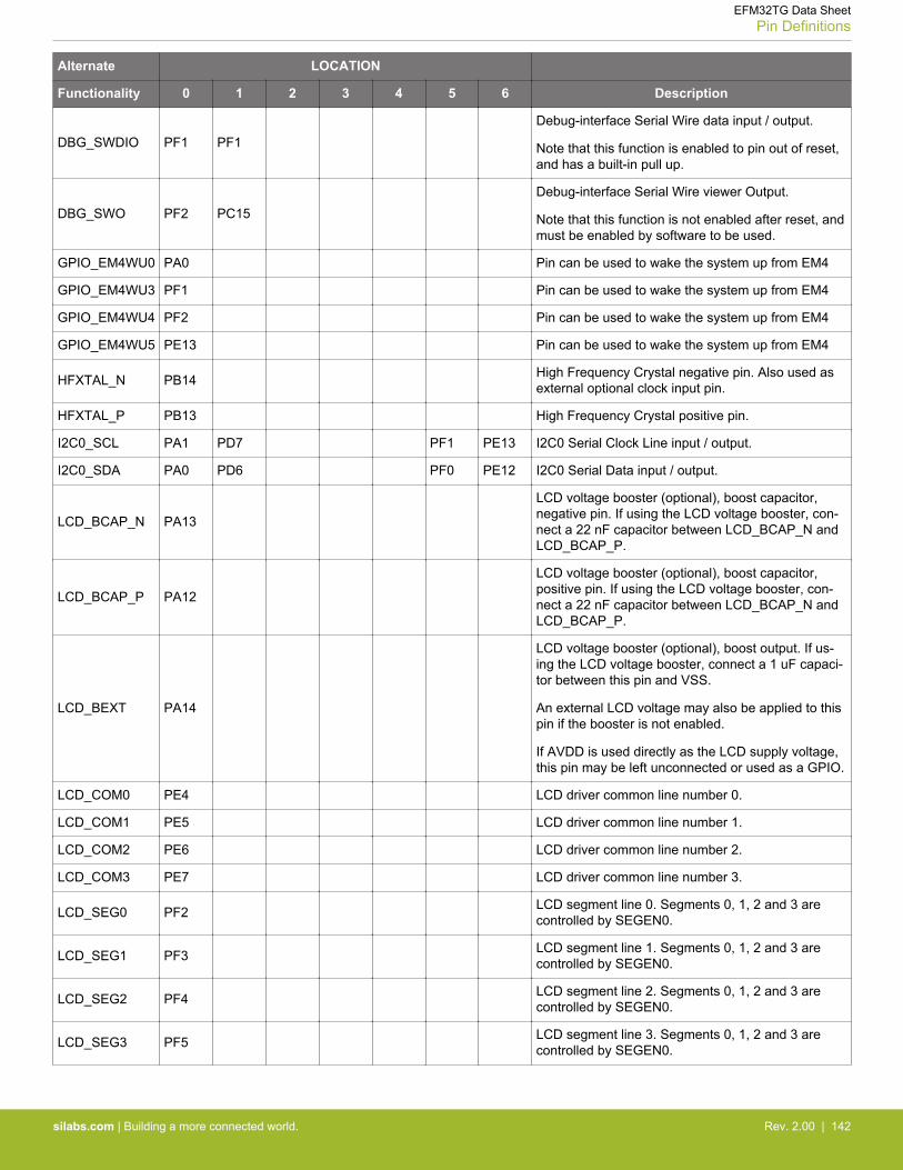
Alternate LOCATION
Functionality 0 1 2 3 4 5 6 Description
DBG_SWDIO PF1 PF1Debug-interface Serial Wire data input / output.
Note that this function is enabled to pin out of reset,and has a built-in pull up.
DBG_SWO PF2 PC15Debug-interface Serial Wire viewer Output.
Note that this function is not enabled after reset, andmust be enabled by software to be used.
GPIO_EM4WU0 PA0 Pin can be used to wake the system up from EM4
GPIO_EM4WU3 PF1 Pin can be used to wake the system up from EM4
GPIO_EM4WU4 PF2 Pin can be used to wake the system up from EM4
GPIO_EM4WU5 PE13 Pin can be used to wake the system up from EM4
HFXTAL_N PB14 High Frequency Crystal negative pin. Also used asexternal optional clock input pin.
HFXTAL_P PB13 High Frequency Crystal positive pin.
I2C0_SCL PA1 PD7 PF1 PE13 I2C0 Serial Clock Line input / output.
I2C0_SDA PA0 PD6 PF0 PE12 I2C0 Serial Data input / output.
LCD_BCAP_N PA13
LCD voltage booster (optional), boost capacitor,negative pin. If using the LCD voltage booster, con-nect a 22 nF capacitor between LCD_BCAP_N andLCD_BCAP_P.
LCD_BCAP_P PA12
LCD voltage booster (optional), boost capacitor,positive pin. If using the LCD voltage booster, con-nect a 22 nF capacitor between LCD_BCAP_N andLCD_BCAP_P.
LCD_BEXT PA14
LCD voltage booster (optional), boost output. If us-ing the LCD voltage booster, connect a 1 uF capaci-tor between this pin and VSS.
An external LCD voltage may also be applied to thispin if the booster is not enabled.
If AVDD is used directly as the LCD supply voltage,this pin may be left unconnected or used as a GPIO.
LCD_COM0 PE4 LCD driver common line number 0.
LCD_COM1 PE5 LCD driver common line number 1.
LCD_COM2 PE6 LCD driver common line number 2.
LCD_COM3 PE7 LCD driver common line number 3.
LCD_SEG0 PF2 LCD segment line 0. Segments 0, 1, 2 and 3 arecontrolled by SEGEN0.
LCD_SEG1 PF3 LCD segment line 1. Segments 0, 1, 2 and 3 arecontrolled by SEGEN0.
LCD_SEG2 PF4 LCD segment line 2. Segments 0, 1, 2 and 3 arecontrolled by SEGEN0.
LCD_SEG3 PF5 LCD segment line 3. Segments 0, 1, 2 and 3 arecontrolled by SEGEN0.
EFM32TG Data SheetPin Definitions
silabs.com | Building a more connected world. Rev. 2.00 | 142

Alternate LOCATION
Functionality 0 1 2 3 4 5 6 Description
LCD_SEG6 PE10 LCD segment line 6. Segments 4, 5, 6 and 7 arecontrolled by SEGEN1.
LCD_SEG7 PE11 LCD segment line 7. Segments 4, 5, 6 and 7 arecontrolled by SEGEN1.
LCD_SEG8 PE12 LCD segment line 8. Segments 8, 9, 10 and 11 arecontrolled by SEGEN2.
LCD_SEG9 PE13 LCD segment line 9. Segments 8, 9, 10 and 11 arecontrolled by SEGEN2.
LCD_SEG13 PA0 LCD segment line 13. Segments 12, 13, 14 and 15are controlled by SEGEN3.
LCD_SEG14 PA1 LCD segment line 14. Segments 12, 13, 14 and 15are controlled by SEGEN3.
LCD_SEG15 PA2 LCD segment line 15. Segments 12, 13, 14 and 15are controlled by SEGEN3.
LCD_SEG20/LCD_COM4 PB3
LCD segment line 20. Segments 20, 21, 22 and 23are controlled by SEGEN5. This pin may also beused as LCD COM line 4
LCD_SEG21/LCD_COM5 PB4
LCD segment line 21. Segments 20, 21, 22 and 23are controlled by SEGEN5. This pin may also beused as LCD COM line 5
LCD_SEG22/LCD_COM6 PB5
LCD segment line 22. Segments 20, 21, 22 and 23are controlled by SEGEN5. This pin may also beused as LCD COM line 6
LCD_SEG23/LCD_COM7 PB6
LCD segment line 23. Segments 20, 21, 22 and 23are controlled by SEGEN5. This pin may also beused as LCD COM line 7
LES_ALTEX0 PD6 LESENSE alternate exite output 0.
LES_ALTEX1 PD7 LESENSE alternate exite output 1.
LES_ALTEX5 PE11 LESENSE alternate exite output 5.
LES_ALTEX6 PE12 LESENSE alternate exite output 6.
LES_ALTEX7 PE13 LESENSE alternate exite output 7.
LES_CH4 PC4 LESENSE channel 4.
LES_CH13 PC13 LESENSE channel 13.
LES_CH14 PC14 LESENSE channel 14.
LES_CH15 PC15 LESENSE channel 15.
LETIM0_OUT0 PD6 PB11 PF0 PC4 Low Energy Timer LETIM0, output channel 0.
LETIM0_OUT1 PD7 PF1 Low Energy Timer LETIM0, output channel 1.
LEU0_RX PD5 PB14 PF1 PA0 LEUART0 Receive input.
LEU0_TX PD4 PB13 PF0 PF2 LEUART0 Transmit output. Also used as receive in-put in half duplex communication.
LFXTAL_N PB8Low Frequency Crystal (typically 32.768 kHz) nega-tive pin. Also used as an optional external clock in-put pin.
EFM32TG Data SheetPin Definitions
silabs.com | Building a more connected world. Rev. 2.00 | 143
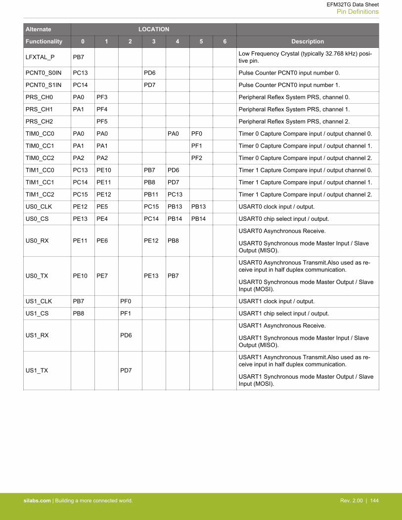
Alternate LOCATION
Functionality 0 1 2 3 4 5 6 Description
LFXTAL_P PB7 Low Frequency Crystal (typically 32.768 kHz) posi-tive pin.
PCNT0_S0IN PC13 PD6 Pulse Counter PCNT0 input number 0.
PCNT0_S1IN PC14 PD7 Pulse Counter PCNT0 input number 1.
PRS_CH0 PA0 PF3 Peripheral Reflex System PRS, channel 0.
PRS_CH1 PA1 PF4 Peripheral Reflex System PRS, channel 1.
PRS_CH2 PF5 Peripheral Reflex System PRS, channel 2.
TIM0_CC0 PA0 PA0 PA0 PF0 Timer 0 Capture Compare input / output channel 0.
TIM0_CC1 PA1 PA1 PF1 Timer 0 Capture Compare input / output channel 1.
TIM0_CC2 PA2 PA2 PF2 Timer 0 Capture Compare input / output channel 2.
TIM1_CC0 PC13 PE10 PB7 PD6 Timer 1 Capture Compare input / output channel 0.
TIM1_CC1 PC14 PE11 PB8 PD7 Timer 1 Capture Compare input / output channel 1.
TIM1_CC2 PC15 PE12 PB11 PC13 Timer 1 Capture Compare input / output channel 2.
US0_CLK PE12 PE5 PC15 PB13 PB13 USART0 clock input / output.
US0_CS PE13 PE4 PC14 PB14 PB14 USART0 chip select input / output.
US0_RX PE11 PE6 PE12 PB8USART0 Asynchronous Receive.
USART0 Synchronous mode Master Input / SlaveOutput (MISO).
US0_TX PE10 PE7 PE13 PB7
USART0 Asynchronous Transmit.Also used as re-ceive input in half duplex communication.
USART0 Synchronous mode Master Output / SlaveInput (MOSI).
US1_CLK PB7 PF0 USART1 clock input / output.
US1_CS PB8 PF1 USART1 chip select input / output.
US1_RX PD6USART1 Asynchronous Receive.
USART1 Synchronous mode Master Input / SlaveOutput (MISO).
US1_TX PD7
USART1 Asynchronous Transmit.Also used as re-ceive input in half duplex communication.
USART1 Synchronous mode Master Output / SlaveInput (MOSI).
EFM32TG Data SheetPin Definitions
silabs.com | Building a more connected world. Rev. 2.00 | 144

5.9.3 GPIO Pinout Overview
The specific GPIO pins available in EFM32TG825 is shown in the following table. Each GPIO port is organized as 16-bit ports indicatedby letters A through F, and the individual pin on this port is indicated by a number from 15 down to 0.
Table 5.27. GPIO Pinout
Port Pin15
Pin14
Pin13
Pin12
Pin11
Pin10
Pin 9 Pin 8 Pin 7 Pin 6 Pin 5 Pin 4 Pin 3 Pin 2 Pin 1 Pin 0
Port A - PA14 PA13 PA12 - - - - - - - - - PA2 PA1 PA0
Port B - PB14 PB13 - PB11 - - PB8 PB7 PB6 PB5 PB4 PB3 - - -
Port C PC15 PC14 PC13 - - - - - - - - PC4 - - - -
Port D - - - - - - - - PD7 PD6 PD5 PD4 - - - -
Port E - - PE13 PE12 PE11 PE10 - - PE7 PE6 PE5 PE4 - - - -
Port F - - - - - - - - - - PF5 PF4 PF3 PF2 PF1 PF0
5.9.4 Opamp Pinout Overview
The specific opamp terminals available in EFM32TG825 is shown in the following figure.
-
+OPA0
-
+OPA2
-
+OPA1
OUT0ALT
OUT0
OUT2
OUT1ALT
OUT1
PC4
PD4
PD6
PD7
PB11
PC13PC14PC15
PD5
Figure 5.17. Opamp Pinout
EFM32TG Data SheetPin Definitions
silabs.com | Building a more connected world. Rev. 2.00 | 145
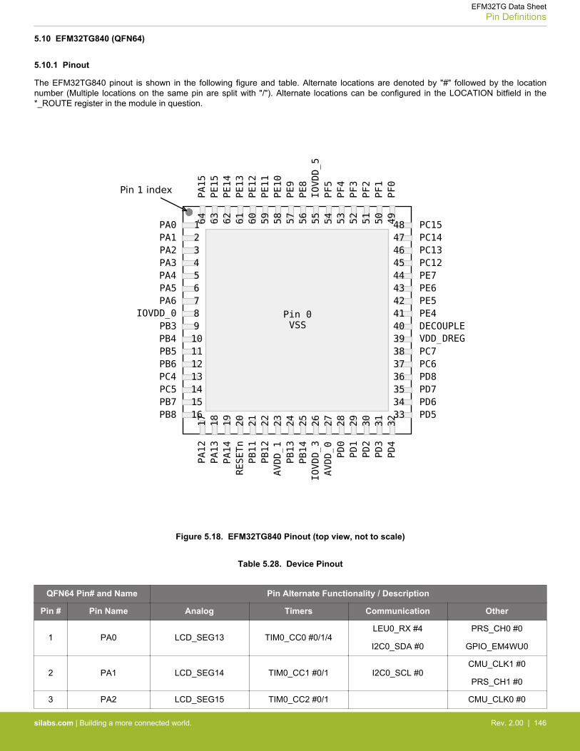
5.10 EFM32TG840 (QFN64)
5.10.1 Pinout
The EFM32TG840 pinout is shown in the following figure and table. Alternate locations are denoted by "#" followed by the locationnumber (Multiple locations on the same pin are split with "/"). Alternate locations can be configured in the LOCATION bitfield in the*_ROUTE register in the module in question.
Figure 5.18. EFM32TG840 Pinout (top view, not to scale)
Table 5.28. Device Pinout
QFN64 Pin# and Name Pin Alternate Functionality / Description
Pin # Pin Name Analog Timers Communication Other
1 PA0 LCD_SEG13 TIM0_CC0 #0/1/4LEU0_RX #4
I2C0_SDA #0
PRS_CH0 #0
GPIO_EM4WU0
2 PA1 LCD_SEG14 TIM0_CC1 #0/1 I2C0_SCL #0CMU_CLK1 #0
PRS_CH1 #0
3 PA2 LCD_SEG15 TIM0_CC2 #0/1 CMU_CLK0 #0
EFM32TG Data SheetPin Definitions
silabs.com | Building a more connected world. Rev. 2.00 | 146
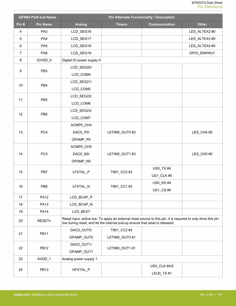
QFN64 Pin# and Name Pin Alternate Functionality / Description
Pin # Pin Name Analog Timers Communication Other
4 PA3 LCD_SEG16 LES_ALTEX2 #0
5 PA4 LCD_SEG17 LES_ALTEX3 #0
6 PA5 LCD_SEG18 LES_ALTEX4 #0
7 PA6 LCD_SEG19 GPIO_EM4WU1
8 IOVDD_0 Digital IO power supply 0.
9 PB3LCD_SEG20/
LCD_COM4
10 PB4LCD_SEG21/
LCD_COM5
11 PB5LCD_SEG22/
LCD_COM6
12 PB6LCD_SEG23/
LCD_COM7
13 PC4
ACMP0_CH4
DAC0_P0/
OPAMP_P0
LETIM0_OUT0 #3 LES_CH4 #0
14 PC5
ACMP0_CH5
DAC0_N0/
OPAMP_N0
LETIM0_OUT1 #3 LES_CH5 #0
15 PB7 LFXTAL_P TIM1_CC0 #3US0_TX #4
US1_CLK #0
16 PB8 LFXTAL_N TIM1_CC1 #3US0_RX #4
US1_CS #0
17 PA12 LCD_BCAP_P
18 PA13 LCD_BCAP_N
19 PA14 LCD_BEXT
20 RESETn Reset input, active low. To apply an external reset source to this pin, it is required to only drive this pinlow during reset, and let the internal pull-up ensure that reset is released.
21 PB11DAC0_OUT0/
OPAMP_OUT0
TIM1_CC2 #3
LETIM0_OUT0 #1
22 PB12DAC0_OUT1/
OPAMP_OUT1LETIM0_OUT1 #1
23 AVDD_1 Analog power supply 1.
24 PB13 HFXTAL_PUS0_CLK #4/5
LEU0_TX #1
EFM32TG Data SheetPin Definitions
silabs.com | Building a more connected world. Rev. 2.00 | 147
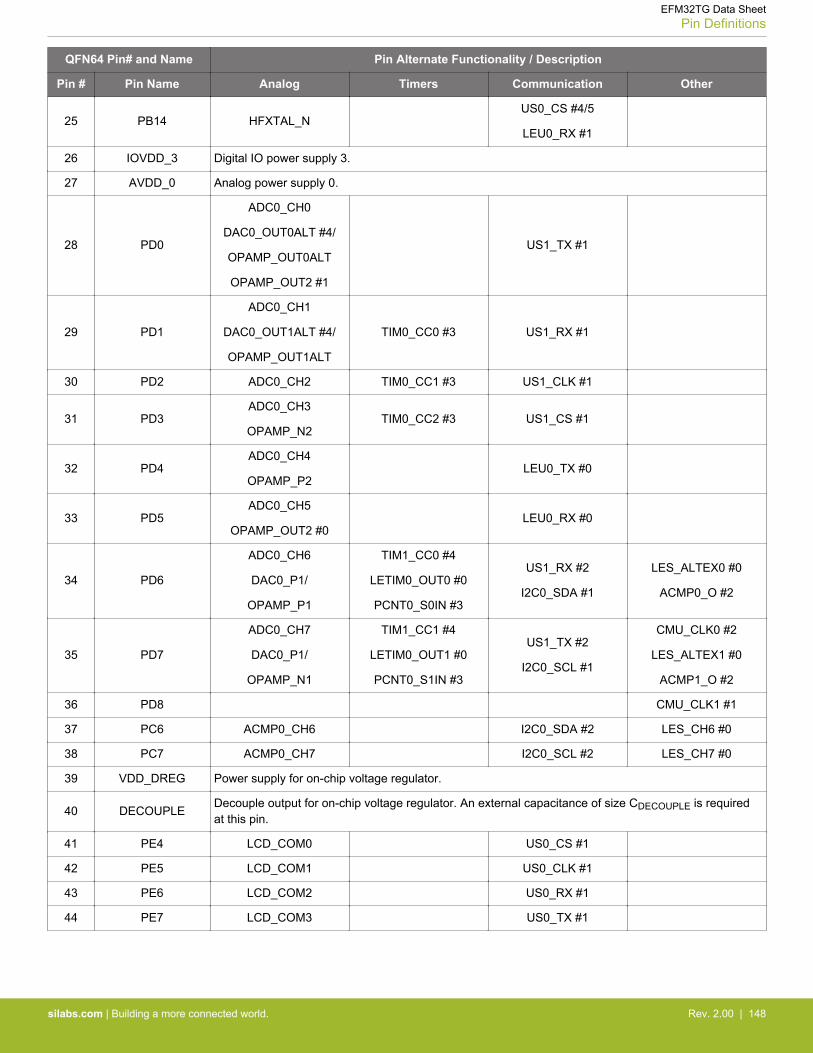
QFN64 Pin# and Name Pin Alternate Functionality / Description
Pin # Pin Name Analog Timers Communication Other
25 PB14 HFXTAL_NUS0_CS #4/5
LEU0_RX #1
26 IOVDD_3 Digital IO power supply 3.
27 AVDD_0 Analog power supply 0.
28 PD0
ADC0_CH0
DAC0_OUT0ALT #4/
OPAMP_OUT0ALT
OPAMP_OUT2 #1
US1_TX #1
29 PD1
ADC0_CH1
DAC0_OUT1ALT #4/
OPAMP_OUT1ALT
TIM0_CC0 #3 US1_RX #1
30 PD2 ADC0_CH2 TIM0_CC1 #3 US1_CLK #1
31 PD3ADC0_CH3
OPAMP_N2TIM0_CC2 #3 US1_CS #1
32 PD4ADC0_CH4
OPAMP_P2LEU0_TX #0
33 PD5ADC0_CH5
OPAMP_OUT2 #0LEU0_RX #0
34 PD6
ADC0_CH6
DAC0_P1/
OPAMP_P1
TIM1_CC0 #4
LETIM0_OUT0 #0
PCNT0_S0IN #3
US1_RX #2
I2C0_SDA #1
LES_ALTEX0 #0
ACMP0_O #2
35 PD7
ADC0_CH7
DAC0_P1/
OPAMP_N1
TIM1_CC1 #4
LETIM0_OUT1 #0
PCNT0_S1IN #3
US1_TX #2
I2C0_SCL #1
CMU_CLK0 #2
LES_ALTEX1 #0
ACMP1_O #2
36 PD8 CMU_CLK1 #1
37 PC6 ACMP0_CH6 I2C0_SDA #2 LES_CH6 #0
38 PC7 ACMP0_CH7 I2C0_SCL #2 LES_CH7 #0
39 VDD_DREG Power supply for on-chip voltage regulator.
40 DECOUPLEDecouple output for on-chip voltage regulator. An external capacitance of size CDECOUPLE is requiredat this pin.
41 PE4 LCD_COM0 US0_CS #1
42 PE5 LCD_COM1 US0_CLK #1
43 PE6 LCD_COM2 US0_RX #1
44 PE7 LCD_COM3 US0_TX #1
EFM32TG Data SheetPin Definitions
silabs.com | Building a more connected world. Rev. 2.00 | 148
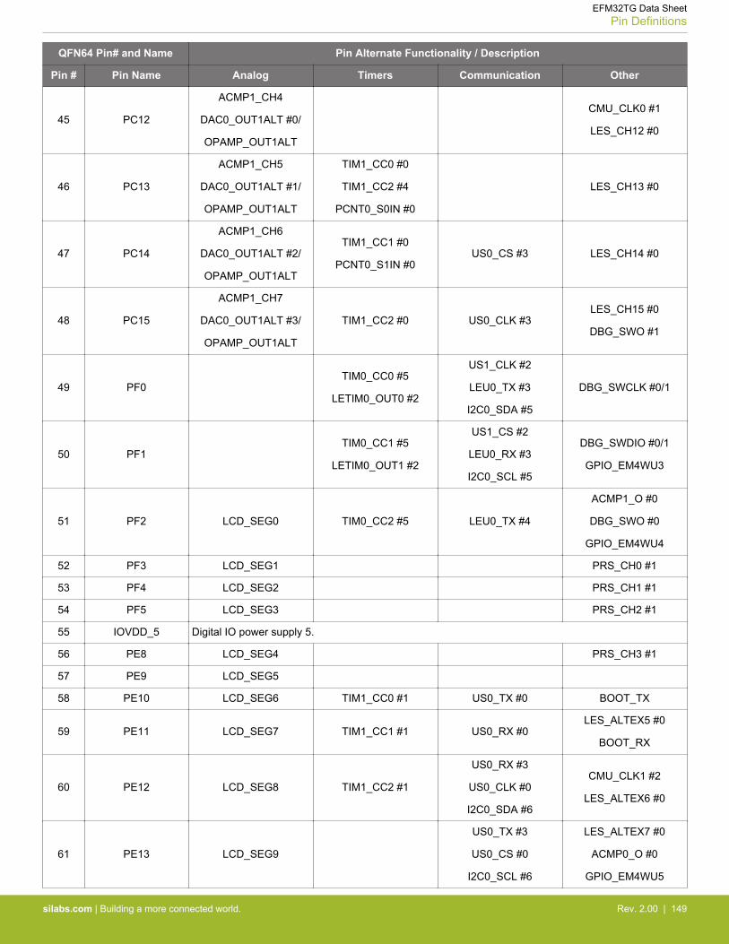
QFN64 Pin# and Name Pin Alternate Functionality / Description
Pin # Pin Name Analog Timers Communication Other
45 PC12
ACMP1_CH4
DAC0_OUT1ALT #0/
OPAMP_OUT1ALT
CMU_CLK0 #1
LES_CH12 #0
46 PC13
ACMP1_CH5
DAC0_OUT1ALT #1/
OPAMP_OUT1ALT
TIM1_CC0 #0
TIM1_CC2 #4
PCNT0_S0IN #0
LES_CH13 #0
47 PC14
ACMP1_CH6
DAC0_OUT1ALT #2/
OPAMP_OUT1ALT
TIM1_CC1 #0
PCNT0_S1IN #0US0_CS #3 LES_CH14 #0
48 PC15
ACMP1_CH7
DAC0_OUT1ALT #3/
OPAMP_OUT1ALT
TIM1_CC2 #0 US0_CLK #3LES_CH15 #0
DBG_SWO #1
49 PF0TIM0_CC0 #5
LETIM0_OUT0 #2
US1_CLK #2
LEU0_TX #3
I2C0_SDA #5
DBG_SWCLK #0/1
50 PF1TIM0_CC1 #5
LETIM0_OUT1 #2
US1_CS #2
LEU0_RX #3
I2C0_SCL #5
DBG_SWDIO #0/1
GPIO_EM4WU3
51 PF2 LCD_SEG0 TIM0_CC2 #5 LEU0_TX #4
ACMP1_O #0
DBG_SWO #0
GPIO_EM4WU4
52 PF3 LCD_SEG1 PRS_CH0 #1
53 PF4 LCD_SEG2 PRS_CH1 #1
54 PF5 LCD_SEG3 PRS_CH2 #1
55 IOVDD_5 Digital IO power supply 5.
56 PE8 LCD_SEG4 PRS_CH3 #1
57 PE9 LCD_SEG5
58 PE10 LCD_SEG6 TIM1_CC0 #1 US0_TX #0 BOOT_TX
59 PE11 LCD_SEG7 TIM1_CC1 #1 US0_RX #0LES_ALTEX5 #0
BOOT_RX
60 PE12 LCD_SEG8 TIM1_CC2 #1
US0_RX #3
US0_CLK #0
I2C0_SDA #6
CMU_CLK1 #2
LES_ALTEX6 #0
61 PE13 LCD_SEG9
US0_TX #3
US0_CS #0
I2C0_SCL #6
LES_ALTEX7 #0
ACMP0_O #0
GPIO_EM4WU5
EFM32TG Data SheetPin Definitions
silabs.com | Building a more connected world. Rev. 2.00 | 149
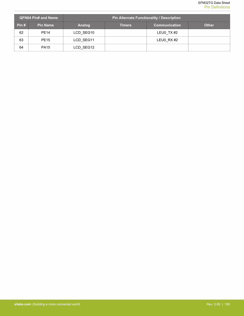
QFN64 Pin# and Name Pin Alternate Functionality / Description
Pin # Pin Name Analog Timers Communication Other
62 PE14 LCD_SEG10 LEU0_TX #2
63 PE15 LCD_SEG11 LEU0_RX #2
64 PA15 LCD_SEG12
EFM32TG Data SheetPin Definitions
silabs.com | Building a more connected world. Rev. 2.00 | 150

5.10.2 Alternate Functionality Pinout
A wide selection of alternate functionality is available for multiplexing to various pins. This is shown in the following table. The tableshows the name of the alternate functionality in the first column, followed by columns showing the possible LOCATION bitfield settings.
Note: Some functionality, such as analog interfaces, do not have alternate settings or a LOCATION bitfield. In these cases, the pinoutis shown in the column corresponding to LOCATION 0.
Table 5.29. Alternate functionality overview
Alternate LOCATION
Functionality 0 1 2 3 4 5 6 Description
ACMP0_CH4 PC4 Analog comparator ACMP0, channel 4.
ACMP0_CH5 PC5 Analog comparator ACMP0, channel 5.
ACMP0_CH6 PC6 Analog comparator ACMP0, channel 6.
ACMP0_CH7 PC7 Analog comparator ACMP0, channel 7.
ACMP0_O PE13 PD6 Analog comparator ACMP0, digital output.
ACMP1_CH4 PC12 Analog comparator ACMP1, channel 4.
ACMP1_CH5 PC13 Analog comparator ACMP1, channel 5.
ACMP1_CH6 PC14 Analog comparator ACMP1, channel 6.
ACMP1_CH7 PC15 Analog comparator ACMP1, channel 7.
ACMP1_O PF2 PD7 Analog comparator ACMP1, digital output.
ADC0_CH0 PD0 Analog to digital converter ADC0, input channelnumber 0.
ADC0_CH1 PD1 Analog to digital converter ADC0, input channelnumber 1.
ADC0_CH2 PD2 Analog to digital converter ADC0, input channelnumber 2.
ADC0_CH3 PD3 Analog to digital converter ADC0, input channelnumber 3.
ADC0_CH4 PD4 Analog to digital converter ADC0, input channelnumber 4.
ADC0_CH5 PD5 Analog to digital converter ADC0, input channelnumber 5.
ADC0_CH6 PD6 Analog to digital converter ADC0, input channelnumber 6.
ADC0_CH7 PD7 Analog to digital converter ADC0, input channelnumber 7.
BOOT_RX PE11 Bootloader RX.
BOOT_TX PE10 Bootloader TX.
CMU_CLK0 PA2 PC12 PD7 Clock Management Unit, clock output number 0.
CMU_CLK1 PA1 PD8 PE12 Clock Management Unit, clock output number 1.
DAC0_N0/OPAMP_N0 PC5 Operational Amplifier 0 external negative input.
DAC0_N1/OPAMP_N1 PD7 Operational Amplifier 1 external negative input.
EFM32TG Data SheetPin Definitions
silabs.com | Building a more connected world. Rev. 2.00 | 151
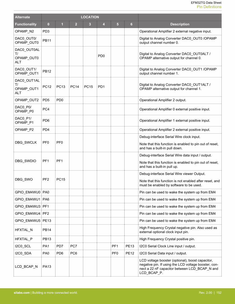
Alternate LOCATION
Functionality 0 1 2 3 4 5 6 Description
OPAMP_N2 PD3 Operational Amplifier 2 external negative input.
DAC0_OUT0/OPAMP_OUT0 PB11 Digital to Analog Converter DAC0_OUT0 /OPAMP
output channel number 0.
DAC0_OUT0ALT/OPAMP_OUT0ALT
PD0 Digital to Analog Converter DAC0_OUT0ALT /OPAMP alternative output for channel 0.
DAC0_OUT1/OPAMP_OUT1 PB12 Digital to Analog Converter DAC0_OUT1 /OPAMP
output channel number 1.
DAC0_OUT1ALT/OPAMP_OUT1ALT
PC12 PC13 PC14 PC15 PD1 Digital to Analog Converter DAC0_OUT1ALT /OPAMP alternative output for channel 1.
OPAMP_OUT2 PD5 PD0 Operational Amplifier 2 output.
DAC0_P0/OPAMP_P0 PC4 Operational Amplifier 0 external positive input.
DAC0_P1/OPAMP_P1 PD6 Operational Amplifier 1 external positive input.
OPAMP_P2 PD4 Operational Amplifier 2 external positive input.
DBG_SWCLK PF0 PF0Debug-interface Serial Wire clock input.
Note that this function is enabled to pin out of reset,and has a built-in pull down.
DBG_SWDIO PF1 PF1Debug-interface Serial Wire data input / output.
Note that this function is enabled to pin out of reset,and has a built-in pull up.
DBG_SWO PF2 PC15Debug-interface Serial Wire viewer Output.
Note that this function is not enabled after reset, andmust be enabled by software to be used.
GPIO_EM4WU0 PA0 Pin can be used to wake the system up from EM4
GPIO_EM4WU1 PA6 Pin can be used to wake the system up from EM4
GPIO_EM4WU3 PF1 Pin can be used to wake the system up from EM4
GPIO_EM4WU4 PF2 Pin can be used to wake the system up from EM4
GPIO_EM4WU5 PE13 Pin can be used to wake the system up from EM4
HFXTAL_N PB14 High Frequency Crystal negative pin. Also used asexternal optional clock input pin.
HFXTAL_P PB13 High Frequency Crystal positive pin.
I2C0_SCL PA1 PD7 PC7 PF1 PE13 I2C0 Serial Clock Line input / output.
I2C0_SDA PA0 PD6 PC6 PF0 PE12 I2C0 Serial Data input / output.
LCD_BCAP_N PA13
LCD voltage booster (optional), boost capacitor,negative pin. If using the LCD voltage booster, con-nect a 22 nF capacitor between LCD_BCAP_N andLCD_BCAP_P.
EFM32TG Data SheetPin Definitions
silabs.com | Building a more connected world. Rev. 2.00 | 152
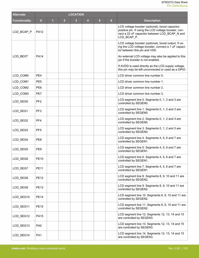
Alternate LOCATION
Functionality 0 1 2 3 4 5 6 Description
LCD_BCAP_P PA12
LCD voltage booster (optional), boost capacitor,positive pin. If using the LCD voltage booster, con-nect a 22 nF capacitor between LCD_BCAP_N andLCD_BCAP_P.
LCD_BEXT PA14
LCD voltage booster (optional), boost output. If us-ing the LCD voltage booster, connect a 1 uF capaci-tor between this pin and VSS.
An external LCD voltage may also be applied to thispin if the booster is not enabled.
If AVDD is used directly as the LCD supply voltage,this pin may be left unconnected or used as a GPIO.
LCD_COM0 PE4 LCD driver common line number 0.
LCD_COM1 PE5 LCD driver common line number 1.
LCD_COM2 PE6 LCD driver common line number 2.
LCD_COM3 PE7 LCD driver common line number 3.
LCD_SEG0 PF2 LCD segment line 0. Segments 0, 1, 2 and 3 arecontrolled by SEGEN0.
LCD_SEG1 PF3 LCD segment line 1. Segments 0, 1, 2 and 3 arecontrolled by SEGEN0.
LCD_SEG2 PF4 LCD segment line 2. Segments 0, 1, 2 and 3 arecontrolled by SEGEN0.
LCD_SEG3 PF5 LCD segment line 3. Segments 0, 1, 2 and 3 arecontrolled by SEGEN0.
LCD_SEG4 PE8 LCD segment line 4. Segments 4, 5, 6 and 7 arecontrolled by SEGEN1.
LCD_SEG5 PE9 LCD segment line 5. Segments 4, 5, 6 and 7 arecontrolled by SEGEN1.
LCD_SEG6 PE10 LCD segment line 6. Segments 4, 5, 6 and 7 arecontrolled by SEGEN1.
LCD_SEG7 PE11 LCD segment line 7. Segments 4, 5, 6 and 7 arecontrolled by SEGEN1.
LCD_SEG8 PE12 LCD segment line 8. Segments 8, 9, 10 and 11 arecontrolled by SEGEN2.
LCD_SEG9 PE13 LCD segment line 9. Segments 8, 9, 10 and 11 arecontrolled by SEGEN2.
LCD_SEG10 PE14 LCD segment line 10. Segments 8, 9, 10 and 11 arecontrolled by SEGEN2.
LCD_SEG11 PE15 LCD segment line 11. Segments 8, 9, 10 and 11 arecontrolled by SEGEN2.
LCD_SEG12 PA15 LCD segment line 12. Segments 12, 13, 14 and 15are controlled by SEGEN3.
LCD_SEG13 PA0 LCD segment line 13. Segments 12, 13, 14 and 15are controlled by SEGEN3.
LCD_SEG14 PA1 LCD segment line 14. Segments 12, 13, 14 and 15are controlled by SEGEN3.
EFM32TG Data SheetPin Definitions
silabs.com | Building a more connected world. Rev. 2.00 | 153
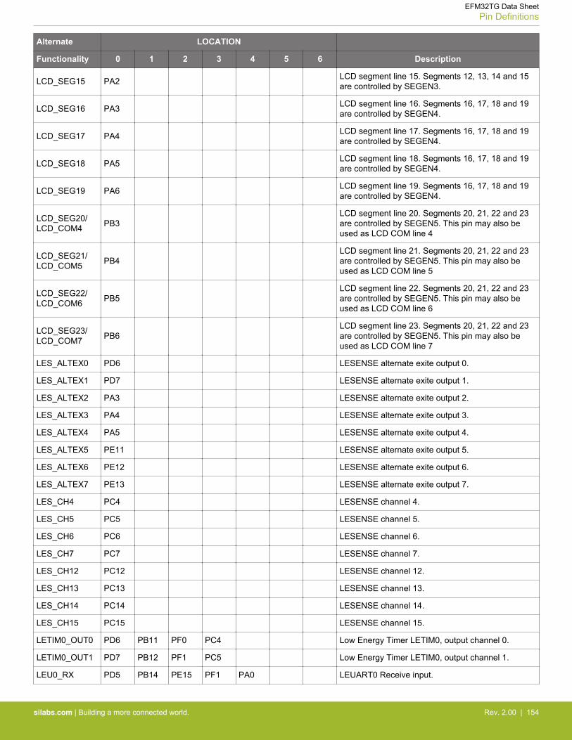
Alternate LOCATION
Functionality 0 1 2 3 4 5 6 Description
LCD_SEG15 PA2 LCD segment line 15. Segments 12, 13, 14 and 15are controlled by SEGEN3.
LCD_SEG16 PA3 LCD segment line 16. Segments 16, 17, 18 and 19are controlled by SEGEN4.
LCD_SEG17 PA4 LCD segment line 17. Segments 16, 17, 18 and 19are controlled by SEGEN4.
LCD_SEG18 PA5 LCD segment line 18. Segments 16, 17, 18 and 19are controlled by SEGEN4.
LCD_SEG19 PA6 LCD segment line 19. Segments 16, 17, 18 and 19are controlled by SEGEN4.
LCD_SEG20/LCD_COM4 PB3
LCD segment line 20. Segments 20, 21, 22 and 23are controlled by SEGEN5. This pin may also beused as LCD COM line 4
LCD_SEG21/LCD_COM5 PB4
LCD segment line 21. Segments 20, 21, 22 and 23are controlled by SEGEN5. This pin may also beused as LCD COM line 5
LCD_SEG22/LCD_COM6 PB5
LCD segment line 22. Segments 20, 21, 22 and 23are controlled by SEGEN5. This pin may also beused as LCD COM line 6
LCD_SEG23/LCD_COM7 PB6
LCD segment line 23. Segments 20, 21, 22 and 23are controlled by SEGEN5. This pin may also beused as LCD COM line 7
LES_ALTEX0 PD6 LESENSE alternate exite output 0.
LES_ALTEX1 PD7 LESENSE alternate exite output 1.
LES_ALTEX2 PA3 LESENSE alternate exite output 2.
LES_ALTEX3 PA4 LESENSE alternate exite output 3.
LES_ALTEX4 PA5 LESENSE alternate exite output 4.
LES_ALTEX5 PE11 LESENSE alternate exite output 5.
LES_ALTEX6 PE12 LESENSE alternate exite output 6.
LES_ALTEX7 PE13 LESENSE alternate exite output 7.
LES_CH4 PC4 LESENSE channel 4.
LES_CH5 PC5 LESENSE channel 5.
LES_CH6 PC6 LESENSE channel 6.
LES_CH7 PC7 LESENSE channel 7.
LES_CH12 PC12 LESENSE channel 12.
LES_CH13 PC13 LESENSE channel 13.
LES_CH14 PC14 LESENSE channel 14.
LES_CH15 PC15 LESENSE channel 15.
LETIM0_OUT0 PD6 PB11 PF0 PC4 Low Energy Timer LETIM0, output channel 0.
LETIM0_OUT1 PD7 PB12 PF1 PC5 Low Energy Timer LETIM0, output channel 1.
LEU0_RX PD5 PB14 PE15 PF1 PA0 LEUART0 Receive input.
EFM32TG Data SheetPin Definitions
silabs.com | Building a more connected world. Rev. 2.00 | 154
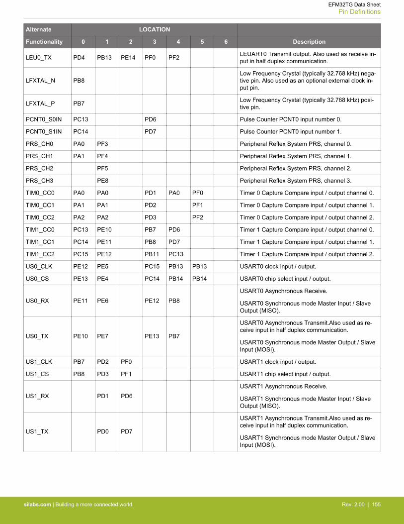
Alternate LOCATION
Functionality 0 1 2 3 4 5 6 Description
LEU0_TX PD4 PB13 PE14 PF0 PF2 LEUART0 Transmit output. Also used as receive in-put in half duplex communication.
LFXTAL_N PB8Low Frequency Crystal (typically 32.768 kHz) nega-tive pin. Also used as an optional external clock in-put pin.
LFXTAL_P PB7 Low Frequency Crystal (typically 32.768 kHz) posi-tive pin.
PCNT0_S0IN PC13 PD6 Pulse Counter PCNT0 input number 0.
PCNT0_S1IN PC14 PD7 Pulse Counter PCNT0 input number 1.
PRS_CH0 PA0 PF3 Peripheral Reflex System PRS, channel 0.
PRS_CH1 PA1 PF4 Peripheral Reflex System PRS, channel 1.
PRS_CH2 PF5 Peripheral Reflex System PRS, channel 2.
PRS_CH3 PE8 Peripheral Reflex System PRS, channel 3.
TIM0_CC0 PA0 PA0 PD1 PA0 PF0 Timer 0 Capture Compare input / output channel 0.
TIM0_CC1 PA1 PA1 PD2 PF1 Timer 0 Capture Compare input / output channel 1.
TIM0_CC2 PA2 PA2 PD3 PF2 Timer 0 Capture Compare input / output channel 2.
TIM1_CC0 PC13 PE10 PB7 PD6 Timer 1 Capture Compare input / output channel 0.
TIM1_CC1 PC14 PE11 PB8 PD7 Timer 1 Capture Compare input / output channel 1.
TIM1_CC2 PC15 PE12 PB11 PC13 Timer 1 Capture Compare input / output channel 2.
US0_CLK PE12 PE5 PC15 PB13 PB13 USART0 clock input / output.
US0_CS PE13 PE4 PC14 PB14 PB14 USART0 chip select input / output.
US0_RX PE11 PE6 PE12 PB8USART0 Asynchronous Receive.
USART0 Synchronous mode Master Input / SlaveOutput (MISO).
US0_TX PE10 PE7 PE13 PB7
USART0 Asynchronous Transmit.Also used as re-ceive input in half duplex communication.
USART0 Synchronous mode Master Output / SlaveInput (MOSI).
US1_CLK PB7 PD2 PF0 USART1 clock input / output.
US1_CS PB8 PD3 PF1 USART1 chip select input / output.
US1_RX PD1 PD6USART1 Asynchronous Receive.
USART1 Synchronous mode Master Input / SlaveOutput (MISO).
US1_TX PD0 PD7
USART1 Asynchronous Transmit.Also used as re-ceive input in half duplex communication.
USART1 Synchronous mode Master Output / SlaveInput (MOSI).
EFM32TG Data SheetPin Definitions
silabs.com | Building a more connected world. Rev. 2.00 | 155
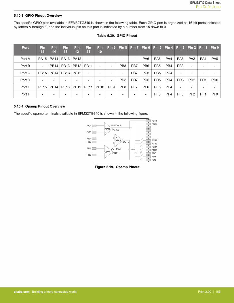
5.10.3 GPIO Pinout Overview
The specific GPIO pins available in EFM32TG840 is shown in the following table. Each GPIO port is organized as 16-bit ports indicatedby letters A through F, and the individual pin on this port is indicated by a number from 15 down to 0.
Table 5.30. GPIO Pinout
Port Pin15
Pin14
Pin13
Pin12
Pin11
Pin10
Pin 9 Pin 8 Pin 7 Pin 6 Pin 5 Pin 4 Pin 3 Pin 2 Pin 1 Pin 0
Port A PA15 PA14 PA13 PA12 - - - - - PA6 PA5 PA4 PA3 PA2 PA1 PA0
Port B - PB14 PB13 PB12 PB11 - - PB8 PB7 PB6 PB5 PB4 PB3 - - -
Port C PC15 PC14 PC13 PC12 - - - - PC7 PC6 PC5 PC4 - - - -
Port D - - - - - - - PD8 PD7 PD6 PD5 PD4 PD3 PD2 PD1 PD0
Port E PE15 PE14 PE13 PE12 PE11 PE10 PE9 PE8 PE7 PE6 PE5 PE4 - - - -
Port F - - - - - - - - - - PF5 PF4 PF3 PF2 PF1 PF0
5.10.4 Opamp Pinout Overview
The specific opamp terminals available in EFM32TG840 is shown in the following figure.
-
+OPA0
-
+OPA2
-
+OPA1
OUT0ALT
OUT0
OUT2
OUT1ALT
OUT1
PC4
PC5
PD4PD3
PD6
PD7
PB11PB12
PC12PC13PC14PC15PD0PD1PD5
Figure 5.19. Opamp Pinout
EFM32TG Data SheetPin Definitions
silabs.com | Building a more connected world. Rev. 2.00 | 156
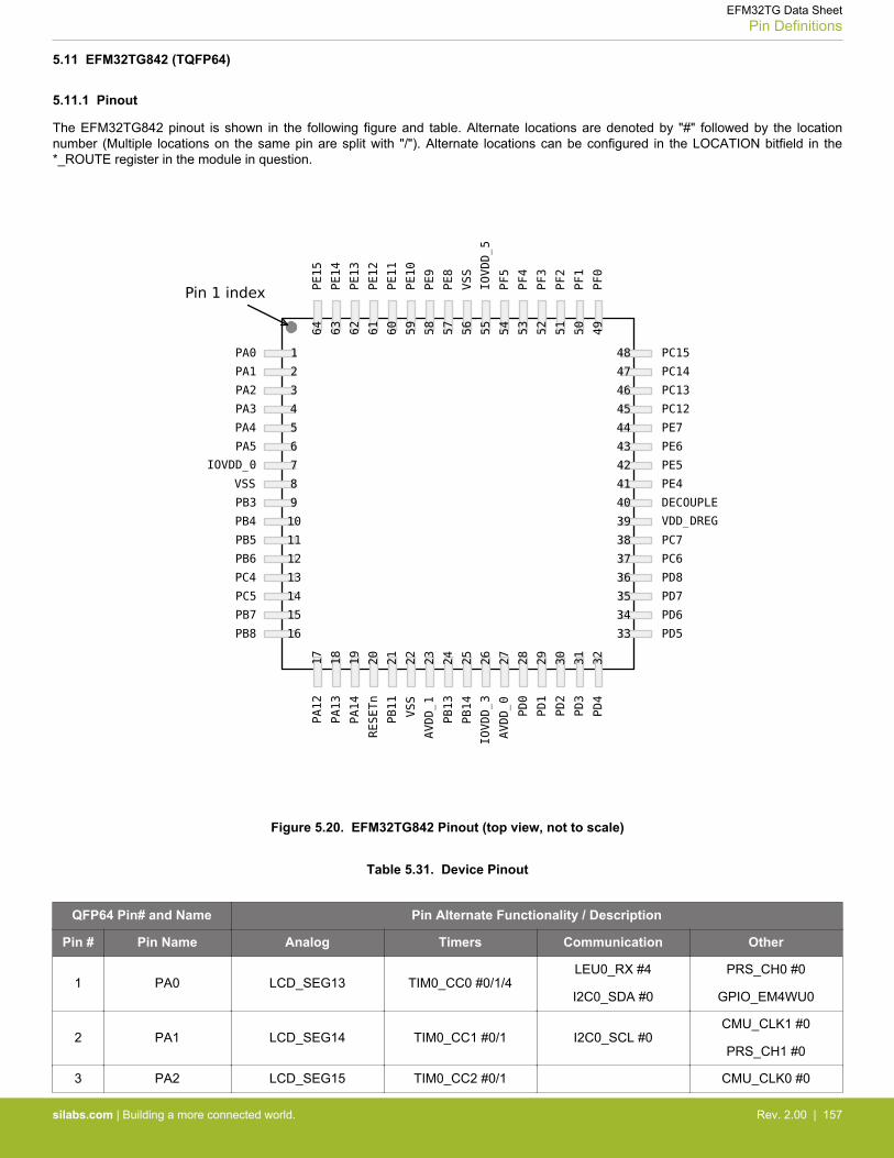
5.11 EFM32TG842 (TQFP64)
5.11.1 Pinout
The EFM32TG842 pinout is shown in the following figure and table. Alternate locations are denoted by "#" followed by the locationnumber (Multiple locations on the same pin are split with "/"). Alternate locations can be configured in the LOCATION bitfield in the*_ROUTE register in the module in question.
Figure 5.20. EFM32TG842 Pinout (top view, not to scale)
Table 5.31. Device Pinout
QFP64 Pin# and Name Pin Alternate Functionality / Description
Pin # Pin Name Analog Timers Communication Other
1 PA0 LCD_SEG13 TIM0_CC0 #0/1/4LEU0_RX #4
I2C0_SDA #0
PRS_CH0 #0
GPIO_EM4WU0
2 PA1 LCD_SEG14 TIM0_CC1 #0/1 I2C0_SCL #0CMU_CLK1 #0
PRS_CH1 #0
3 PA2 LCD_SEG15 TIM0_CC2 #0/1 CMU_CLK0 #0
EFM32TG Data SheetPin Definitions
silabs.com | Building a more connected world. Rev. 2.00 | 157
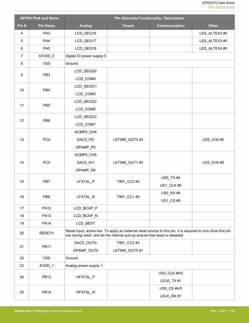
QFP64 Pin# and Name Pin Alternate Functionality / Description
Pin # Pin Name Analog Timers Communication Other
4 PA3 LCD_SEG16 LES_ALTEX2 #0
5 PA4 LCD_SEG17 LES_ALTEX3 #0
6 PA5 LCD_SEG18 LES_ALTEX4 #0
7 IOVDD_0 Digital IO power supply 0.
8 VSS Ground.
9 PB3LCD_SEG20/
LCD_COM4
10 PB4LCD_SEG21/
LCD_COM5
11 PB5LCD_SEG22/
LCD_COM6
12 PB6LCD_SEG23/
LCD_COM7
13 PC4
ACMP0_CH4
DAC0_P0/
OPAMP_P0
LETIM0_OUT0 #3 LES_CH4 #0
14 PC5
ACMP0_CH5
DAC0_N1/
OPAMP_N0
LETIM0_OUT1 #3 LES_CH5 #0
15 PB7 LFXTAL_P TIM1_CC0 #3US0_TX #4
US1_CLK #0
16 PB8 LFXTAL_N TIM1_CC1 #3US0_RX #4
US1_CS #0
17 PA12 LCD_BCAP_P
18 PA13 LCD_BCAP_N
19 PA14 LCD_BEXT
20 RESETn Reset input, active low. To apply an external reset source to this pin, it is required to only drive this pinlow during reset, and let the internal pull-up ensure that reset is released.
21 PB11DAC0_OUT0/
OPAMP_OUT0
TIM1_CC2 #3
LETIM0_OUT0 #1
22 VSS Ground.
23 AVDD_1 Analog power supply 1.
24 PB13 HFXTAL_PUS0_CLK #4/5
LEU0_TX #1
25 PB14 HFXTAL_NUS0_CS #4/5
LEU0_RX #1
EFM32TG Data SheetPin Definitions
silabs.com | Building a more connected world. Rev. 2.00 | 158
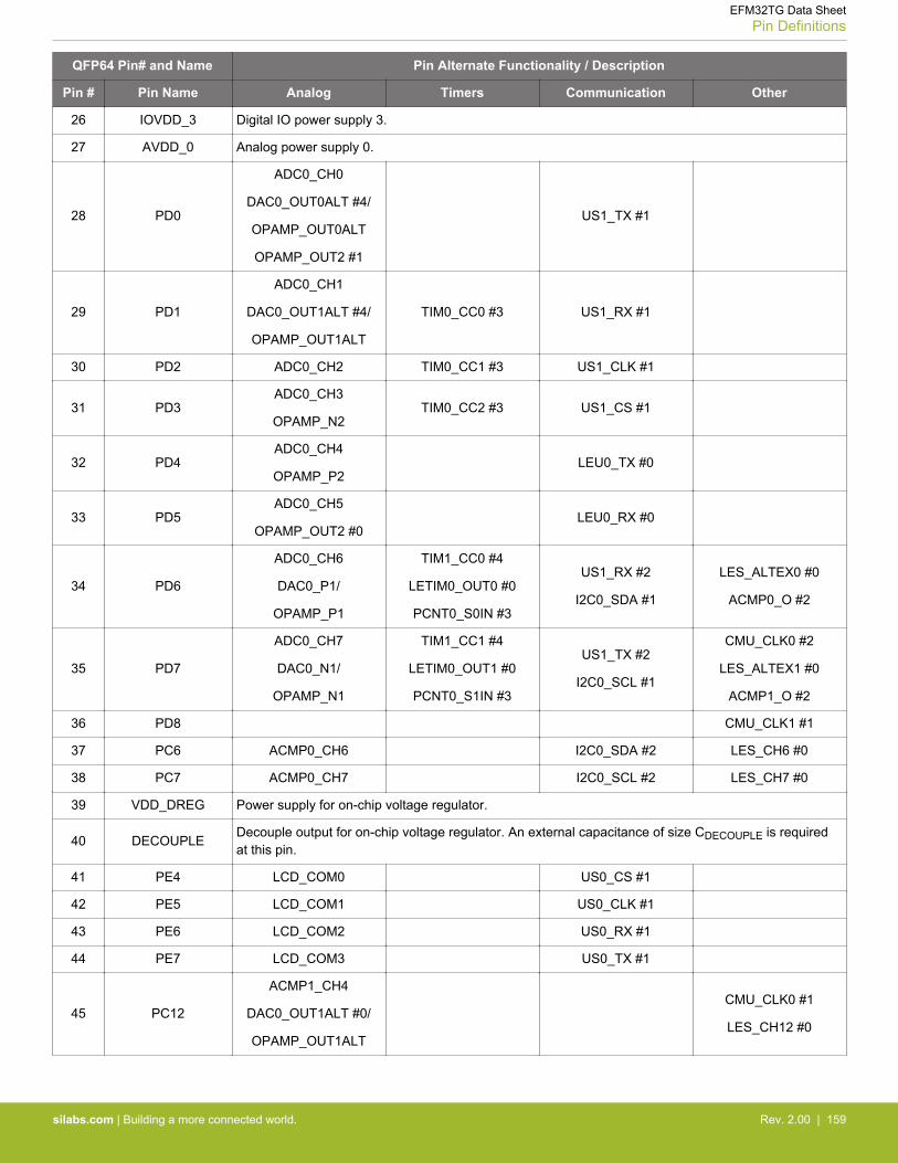
QFP64 Pin# and Name Pin Alternate Functionality / Description
Pin # Pin Name Analog Timers Communication Other
26 IOVDD_3 Digital IO power supply 3.
27 AVDD_0 Analog power supply 0.
28 PD0
ADC0_CH0
DAC0_OUT0ALT #4/
OPAMP_OUT0ALT
OPAMP_OUT2 #1
US1_TX #1
29 PD1
ADC0_CH1
DAC0_OUT1ALT #4/
OPAMP_OUT1ALT
TIM0_CC0 #3 US1_RX #1
30 PD2 ADC0_CH2 TIM0_CC1 #3 US1_CLK #1
31 PD3ADC0_CH3
OPAMP_N2TIM0_CC2 #3 US1_CS #1
32 PD4ADC0_CH4
OPAMP_P2LEU0_TX #0
33 PD5ADC0_CH5
OPAMP_OUT2 #0LEU0_RX #0
34 PD6
ADC0_CH6
DAC0_P1/
OPAMP_P1
TIM1_CC0 #4
LETIM0_OUT0 #0
PCNT0_S0IN #3
US1_RX #2
I2C0_SDA #1
LES_ALTEX0 #0
ACMP0_O #2
35 PD7
ADC0_CH7
DAC0_N1/
OPAMP_N1
TIM1_CC1 #4
LETIM0_OUT1 #0
PCNT0_S1IN #3
US1_TX #2
I2C0_SCL #1
CMU_CLK0 #2
LES_ALTEX1 #0
ACMP1_O #2
36 PD8 CMU_CLK1 #1
37 PC6 ACMP0_CH6 I2C0_SDA #2 LES_CH6 #0
38 PC7 ACMP0_CH7 I2C0_SCL #2 LES_CH7 #0
39 VDD_DREG Power supply for on-chip voltage regulator.
40 DECOUPLEDecouple output for on-chip voltage regulator. An external capacitance of size CDECOUPLE is requiredat this pin.
41 PE4 LCD_COM0 US0_CS #1
42 PE5 LCD_COM1 US0_CLK #1
43 PE6 LCD_COM2 US0_RX #1
44 PE7 LCD_COM3 US0_TX #1
45 PC12
ACMP1_CH4
DAC0_OUT1ALT #0/
OPAMP_OUT1ALT
CMU_CLK0 #1
LES_CH12 #0
EFM32TG Data SheetPin Definitions
silabs.com | Building a more connected world. Rev. 2.00 | 159
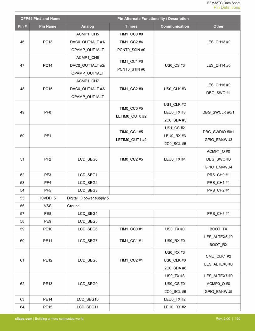
QFP64 Pin# and Name Pin Alternate Functionality / Description
Pin # Pin Name Analog Timers Communication Other
46 PC13
ACMP1_CH5
DAC0_OUT1ALT #1/
OPAMP_OUT1ALT
TIM1_CC0 #0
TIM1_CC2 #4
PCNT0_S0IN #0
LES_CH13 #0
47 PC14
ACMP1_CH6
DAC0_OUT1ALT #2/
OPAMP_OUT1ALT
TIM1_CC1 #0
PCNT0_S1IN #0US0_CS #3 LES_CH14 #0
48 PC15
ACMP1_CH7
DAC0_OUT1ALT #3/
OPAMP_OUT1ALT
TIM1_CC2 #0 US0_CLK #3LES_CH15 #0
DBG_SWO #1
49 PF0TIM0_CC0 #5
LETIM0_OUT0 #2
US1_CLK #2
LEU0_TX #3
I2C0_SDA #5
DBG_SWCLK #0/1
50 PF1TIM0_CC1 #5
LETIM0_OUT1 #2
US1_CS #2
LEU0_RX #3
I2C0_SCL #5
DBG_SWDIO #0/1
GPIO_EM4WU3
51 PF2 LCD_SEG0 TIM0_CC2 #5 LEU0_TX #4
ACMP1_O #0
DBG_SWO #0
GPIO_EM4WU4
52 PF3 LCD_SEG1 PRS_CH0 #1
53 PF4 LCD_SEG2 PRS_CH1 #1
54 PF5 LCD_SEG3 PRS_CH2 #1
55 IOVDD_5 Digital IO power supply 5.
56 VSS Ground.
57 PE8 LCD_SEG4 PRS_CH3 #1
58 PE9 LCD_SEG5
59 PE10 LCD_SEG6 TIM1_CC0 #1 US0_TX #0 BOOT_TX
60 PE11 LCD_SEG7 TIM1_CC1 #1 US0_RX #0LES_ALTEX5 #0
BOOT_RX
61 PE12 LCD_SEG8 TIM1_CC2 #1
US0_RX #3
US0_CLK #0
I2C0_SDA #6
CMU_CLK1 #2
LES_ALTEX6 #0
62 PE13 LCD_SEG9
US0_TX #3
US0_CS #0
I2C0_SCL #6
LES_ALTEX7 #0
ACMP0_O #0
GPIO_EM4WU5
63 PE14 LCD_SEG10 LEU0_TX #2
64 PE15 LCD_SEG11 LEU0_RX #2
EFM32TG Data SheetPin Definitions
silabs.com | Building a more connected world. Rev. 2.00 | 160
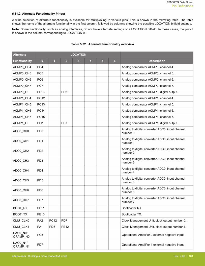
5.11.2 Alternate Functionality Pinout
A wide selection of alternate functionality is available for multiplexing to various pins. This is shown in the following table. The tableshows the name of the alternate functionality in the first column, followed by columns showing the possible LOCATION bitfield settings.
Note: Some functionality, such as analog interfaces, do not have alternate settings or a LOCATION bitfield. In these cases, the pinoutis shown in the column corresponding to LOCATION 0.
Table 5.32. Alternate functionality overview
Alternate LOCATION
Functionality 0 1 2 3 4 5 6 Description
ACMP0_CH4 PC4 Analog comparator ACMP0, channel 4.
ACMP0_CH5 PC5 Analog comparator ACMP0, channel 5.
ACMP0_CH6 PC6 Analog comparator ACMP0, channel 6.
ACMP0_CH7 PC7 Analog comparator ACMP0, channel 7.
ACMP0_O PE13 PD6 Analog comparator ACMP0, digital output.
ACMP1_CH4 PC12 Analog comparator ACMP1, channel 4.
ACMP1_CH5 PC13 Analog comparator ACMP1, channel 5.
ACMP1_CH6 PC14 Analog comparator ACMP1, channel 6.
ACMP1_CH7 PC15 Analog comparator ACMP1, channel 7.
ACMP1_O PF2 PD7 Analog comparator ACMP1, digital output.
ADC0_CH0 PD0 Analog to digital converter ADC0, input channelnumber 0.
ADC0_CH1 PD1 Analog to digital converter ADC0, input channelnumber 1.
ADC0_CH2 PD2 Analog to digital converter ADC0, input channelnumber 2.
ADC0_CH3 PD3 Analog to digital converter ADC0, input channelnumber 3.
ADC0_CH4 PD4 Analog to digital converter ADC0, input channelnumber 4.
ADC0_CH5 PD5 Analog to digital converter ADC0, input channelnumber 5.
ADC0_CH6 PD6 Analog to digital converter ADC0, input channelnumber 6.
ADC0_CH7 PD7 Analog to digital converter ADC0, input channelnumber 7.
BOOT_RX PE11 Bootloader RX.
BOOT_TX PE10 Bootloader TX.
CMU_CLK0 PA2 PC12 PD7 Clock Management Unit, clock output number 0.
CMU_CLK1 PA1 PD8 PE12 Clock Management Unit, clock output number 1.
DAC0_N0/OPAMP_N0 PC5 Operational Amplifier 0 external negative input.
DAC0_N1/OPAMP_N1 PD7 Operational Amplifier 1 external negative input.
EFM32TG Data SheetPin Definitions
silabs.com | Building a more connected world. Rev. 2.00 | 161
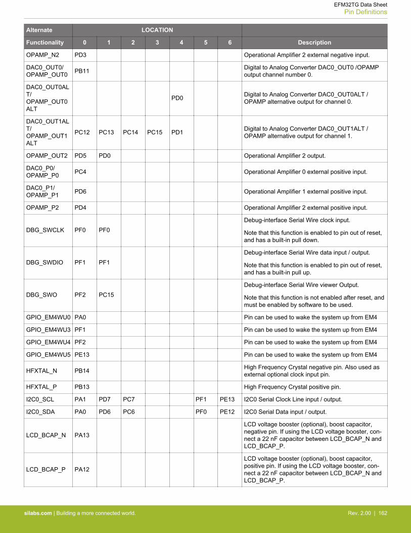
Alternate LOCATION
Functionality 0 1 2 3 4 5 6 Description
OPAMP_N2 PD3 Operational Amplifier 2 external negative input.
DAC0_OUT0/OPAMP_OUT0 PB11 Digital to Analog Converter DAC0_OUT0 /OPAMP
output channel number 0.
DAC0_OUT0ALT/OPAMP_OUT0ALT
PD0 Digital to Analog Converter DAC0_OUT0ALT /OPAMP alternative output for channel 0.
DAC0_OUT1ALT/OPAMP_OUT1ALT
PC12 PC13 PC14 PC15 PD1 Digital to Analog Converter DAC0_OUT1ALT /OPAMP alternative output for channel 1.
OPAMP_OUT2 PD5 PD0 Operational Amplifier 2 output.
DAC0_P0/OPAMP_P0 PC4 Operational Amplifier 0 external positive input.
DAC0_P1/OPAMP_P1 PD6 Operational Amplifier 1 external positive input.
OPAMP_P2 PD4 Operational Amplifier 2 external positive input.
DBG_SWCLK PF0 PF0Debug-interface Serial Wire clock input.
Note that this function is enabled to pin out of reset,and has a built-in pull down.
DBG_SWDIO PF1 PF1Debug-interface Serial Wire data input / output.
Note that this function is enabled to pin out of reset,and has a built-in pull up.
DBG_SWO PF2 PC15Debug-interface Serial Wire viewer Output.
Note that this function is not enabled after reset, andmust be enabled by software to be used.
GPIO_EM4WU0 PA0 Pin can be used to wake the system up from EM4
GPIO_EM4WU3 PF1 Pin can be used to wake the system up from EM4
GPIO_EM4WU4 PF2 Pin can be used to wake the system up from EM4
GPIO_EM4WU5 PE13 Pin can be used to wake the system up from EM4
HFXTAL_N PB14 High Frequency Crystal negative pin. Also used asexternal optional clock input pin.
HFXTAL_P PB13 High Frequency Crystal positive pin.
I2C0_SCL PA1 PD7 PC7 PF1 PE13 I2C0 Serial Clock Line input / output.
I2C0_SDA PA0 PD6 PC6 PF0 PE12 I2C0 Serial Data input / output.
LCD_BCAP_N PA13
LCD voltage booster (optional), boost capacitor,negative pin. If using the LCD voltage booster, con-nect a 22 nF capacitor between LCD_BCAP_N andLCD_BCAP_P.
LCD_BCAP_P PA12
LCD voltage booster (optional), boost capacitor,positive pin. If using the LCD voltage booster, con-nect a 22 nF capacitor between LCD_BCAP_N andLCD_BCAP_P.
EFM32TG Data SheetPin Definitions
silabs.com | Building a more connected world. Rev. 2.00 | 162
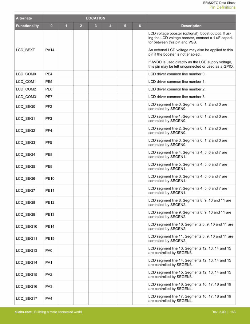
Alternate LOCATION
Functionality 0 1 2 3 4 5 6 Description
LCD_BEXT PA14
LCD voltage booster (optional), boost output. If us-ing the LCD voltage booster, connect a 1 uF capaci-tor between this pin and VSS.
An external LCD voltage may also be applied to thispin if the booster is not enabled.
If AVDD is used directly as the LCD supply voltage,this pin may be left unconnected or used as a GPIO.
LCD_COM0 PE4 LCD driver common line number 0.
LCD_COM1 PE5 LCD driver common line number 1.
LCD_COM2 PE6 LCD driver common line number 2.
LCD_COM3 PE7 LCD driver common line number 3.
LCD_SEG0 PF2 LCD segment line 0. Segments 0, 1, 2 and 3 arecontrolled by SEGEN0.
LCD_SEG1 PF3 LCD segment line 1. Segments 0, 1, 2 and 3 arecontrolled by SEGEN0.
LCD_SEG2 PF4 LCD segment line 2. Segments 0, 1, 2 and 3 arecontrolled by SEGEN0.
LCD_SEG3 PF5 LCD segment line 3. Segments 0, 1, 2 and 3 arecontrolled by SEGEN0.
LCD_SEG4 PE8 LCD segment line 4. Segments 4, 5, 6 and 7 arecontrolled by SEGEN1.
LCD_SEG5 PE9 LCD segment line 5. Segments 4, 5, 6 and 7 arecontrolled by SEGEN1.
LCD_SEG6 PE10 LCD segment line 6. Segments 4, 5, 6 and 7 arecontrolled by SEGEN1.
LCD_SEG7 PE11 LCD segment line 7. Segments 4, 5, 6 and 7 arecontrolled by SEGEN1.
LCD_SEG8 PE12 LCD segment line 8. Segments 8, 9, 10 and 11 arecontrolled by SEGEN2.
LCD_SEG9 PE13 LCD segment line 9. Segments 8, 9, 10 and 11 arecontrolled by SEGEN2.
LCD_SEG10 PE14 LCD segment line 10. Segments 8, 9, 10 and 11 arecontrolled by SEGEN2.
LCD_SEG11 PE15 LCD segment line 11. Segments 8, 9, 10 and 11 arecontrolled by SEGEN2.
LCD_SEG13 PA0 LCD segment line 13. Segments 12, 13, 14 and 15are controlled by SEGEN3.
LCD_SEG14 PA1 LCD segment line 14. Segments 12, 13, 14 and 15are controlled by SEGEN3.
LCD_SEG15 PA2 LCD segment line 15. Segments 12, 13, 14 and 15are controlled by SEGEN3.
LCD_SEG16 PA3 LCD segment line 16. Segments 16, 17, 18 and 19are controlled by SEGEN4.
LCD_SEG17 PA4 LCD segment line 17. Segments 16, 17, 18 and 19are controlled by SEGEN4.
EFM32TG Data SheetPin Definitions
silabs.com | Building a more connected world. Rev. 2.00 | 163
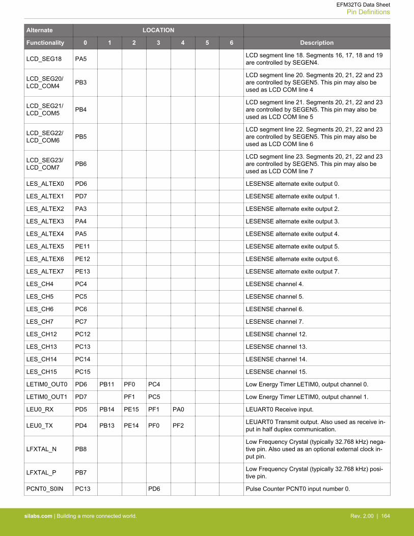
Alternate LOCATION
Functionality 0 1 2 3 4 5 6 Description
LCD_SEG18 PA5 LCD segment line 18. Segments 16, 17, 18 and 19are controlled by SEGEN4.
LCD_SEG20/LCD_COM4 PB3
LCD segment line 20. Segments 20, 21, 22 and 23are controlled by SEGEN5. This pin may also beused as LCD COM line 4
LCD_SEG21/LCD_COM5 PB4
LCD segment line 21. Segments 20, 21, 22 and 23are controlled by SEGEN5. This pin may also beused as LCD COM line 5
LCD_SEG22/LCD_COM6 PB5
LCD segment line 22. Segments 20, 21, 22 and 23are controlled by SEGEN5. This pin may also beused as LCD COM line 6
LCD_SEG23/LCD_COM7 PB6
LCD segment line 23. Segments 20, 21, 22 and 23are controlled by SEGEN5. This pin may also beused as LCD COM line 7
LES_ALTEX0 PD6 LESENSE alternate exite output 0.
LES_ALTEX1 PD7 LESENSE alternate exite output 1.
LES_ALTEX2 PA3 LESENSE alternate exite output 2.
LES_ALTEX3 PA4 LESENSE alternate exite output 3.
LES_ALTEX4 PA5 LESENSE alternate exite output 4.
LES_ALTEX5 PE11 LESENSE alternate exite output 5.
LES_ALTEX6 PE12 LESENSE alternate exite output 6.
LES_ALTEX7 PE13 LESENSE alternate exite output 7.
LES_CH4 PC4 LESENSE channel 4.
LES_CH5 PC5 LESENSE channel 5.
LES_CH6 PC6 LESENSE channel 6.
LES_CH7 PC7 LESENSE channel 7.
LES_CH12 PC12 LESENSE channel 12.
LES_CH13 PC13 LESENSE channel 13.
LES_CH14 PC14 LESENSE channel 14.
LES_CH15 PC15 LESENSE channel 15.
LETIM0_OUT0 PD6 PB11 PF0 PC4 Low Energy Timer LETIM0, output channel 0.
LETIM0_OUT1 PD7 PF1 PC5 Low Energy Timer LETIM0, output channel 1.
LEU0_RX PD5 PB14 PE15 PF1 PA0 LEUART0 Receive input.
LEU0_TX PD4 PB13 PE14 PF0 PF2 LEUART0 Transmit output. Also used as receive in-put in half duplex communication.
LFXTAL_N PB8Low Frequency Crystal (typically 32.768 kHz) nega-tive pin. Also used as an optional external clock in-put pin.
LFXTAL_P PB7 Low Frequency Crystal (typically 32.768 kHz) posi-tive pin.
PCNT0_S0IN PC13 PD6 Pulse Counter PCNT0 input number 0.
EFM32TG Data SheetPin Definitions
silabs.com | Building a more connected world. Rev. 2.00 | 164
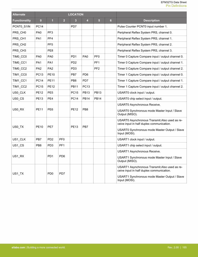
Alternate LOCATION
Functionality 0 1 2 3 4 5 6 Description
PCNT0_S1IN PC14 PD7 Pulse Counter PCNT0 input number 1.
PRS_CH0 PA0 PF3 Peripheral Reflex System PRS, channel 0.
PRS_CH1 PA1 PF4 Peripheral Reflex System PRS, channel 1.
PRS_CH2 PF5 Peripheral Reflex System PRS, channel 2.
PRS_CH3 PE8 Peripheral Reflex System PRS, channel 3.
TIM0_CC0 PA0 PA0 PD1 PA0 PF0 Timer 0 Capture Compare input / output channel 0.
TIM0_CC1 PA1 PA1 PD2 PF1 Timer 0 Capture Compare input / output channel 1.
TIM0_CC2 PA2 PA2 PD3 PF2 Timer 0 Capture Compare input / output channel 2.
TIM1_CC0 PC13 PE10 PB7 PD6 Timer 1 Capture Compare input / output channel 0.
TIM1_CC1 PC14 PE11 PB8 PD7 Timer 1 Capture Compare input / output channel 1.
TIM1_CC2 PC15 PE12 PB11 PC13 Timer 1 Capture Compare input / output channel 2.
US0_CLK PE12 PE5 PC15 PB13 PB13 USART0 clock input / output.
US0_CS PE13 PE4 PC14 PB14 PB14 USART0 chip select input / output.
US0_RX PE11 PE6 PE12 PB8USART0 Asynchronous Receive.
USART0 Synchronous mode Master Input / SlaveOutput (MISO).
US0_TX PE10 PE7 PE13 PB7
USART0 Asynchronous Transmit.Also used as re-ceive input in half duplex communication.
USART0 Synchronous mode Master Output / SlaveInput (MOSI).
US1_CLK PB7 PD2 PF0 USART1 clock input / output.
US1_CS PB8 PD3 PF1 USART1 chip select input / output.
US1_RX PD1 PD6USART1 Asynchronous Receive.
USART1 Synchronous mode Master Input / SlaveOutput (MISO).
US1_TX PD0 PD7
USART1 Asynchronous Transmit.Also used as re-ceive input in half duplex communication.
USART1 Synchronous mode Master Output / SlaveInput (MOSI).
EFM32TG Data SheetPin Definitions
silabs.com | Building a more connected world. Rev. 2.00 | 165

5.11.3 GPIO Pinout Overview
The specific GPIO pins available in EFM32TG842 is shown in the following table. Each GPIO port is organized as 16-bit ports indicatedby letters A through F, and the individual pin on this port is indicated by a number from 15 down to 0.
Table 5.33. GPIO Pinout
Port Pin15
Pin14
Pin13
Pin12
Pin11
Pin10
Pin 9 Pin 8 Pin 7 Pin 6 Pin 5 Pin 4 Pin 3 Pin 2 Pin 1 Pin 0
Port A - PA14 PA13 PA12 - - - - - - PA5 PA4 PA3 PA2 PA1 PA0
Port B - PB14 PB13 - PB11 - - PB8 PB7 PB6 PB5 PB4 PB3 - - -
Port C PC15 PC14 PC13 PC12 - - - - PC7 PC6 PC5 PC4 - - - -
Port D - - - - - - - PD8 PD7 PD6 PD5 PD4 PD3 PD2 PD1 PD0
Port E PE15 PE14 PE13 PE12 PE11 PE10 PE9 PE8 PE7 PE6 PE5 PE4 - - - -
Port F - - - - - - - - - - PF5 PF4 PF3 PF2 PF1 PF0
5.11.4 Opamp Pinout Overview
The specific opamp terminals available in EFM32TG842 is shown in the following figure.
-
+OPA0
-
+OPA2
-
+OPA1
OUT0ALT
OUT0
OUT2
OUT1ALT
OUT1
PC4
PC5
PD4PD3
PD6
PD7
PB11
PC12PC13PC14PC15PD0PD1PD5
Figure 5.21. Opamp Pinout
EFM32TG Data SheetPin Definitions
silabs.com | Building a more connected world. Rev. 2.00 | 166
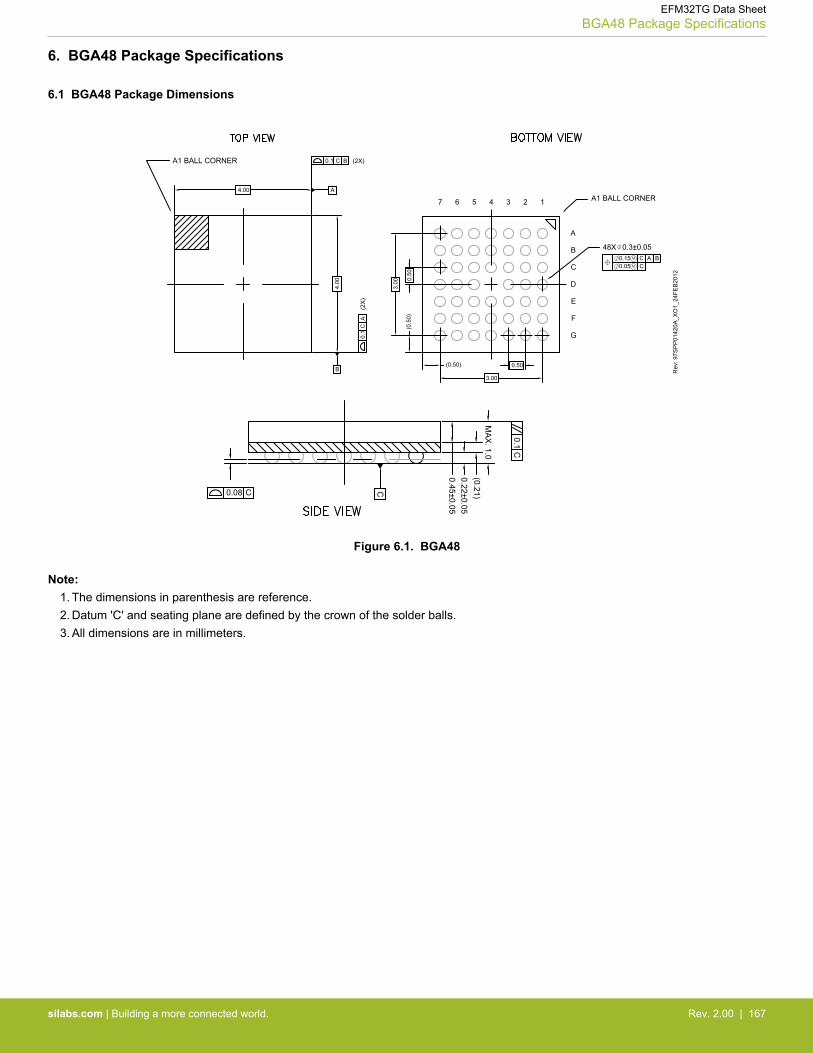
6. BGA48 Package Specifications
6.1 BGA48 Package Dimensions
Rev
: 97S
PP
0142
0A_X
O1_
24FE
B20
12
1234567
A
B
C
D
E
F
G
48X 0.3±0.050.15 C A B0.05 C
A1 BALL CORNER
A1 BALL CORNER
4.00
4.00
3.00
0.50(0.50)
3.00 0.
50(0
.50)
0.45±0.050.22±0.05(0.21)
MA
X. 1.0
A
0.1 C B (2X)
B0.
1C
A(2
X)
C0.08 C
SIDE VIEW
BOTTOM VIEW
0.1C
Figure 6.1. BGA48
Note:1. The dimensions in parenthesis are reference.2. Datum 'C' and seating plane are defined by the crown of the solder balls.3. All dimensions are in millimeters.
EFM32TG Data SheetBGA48 Package Specifications
silabs.com | Building a more connected world. Rev. 2.00 | 167
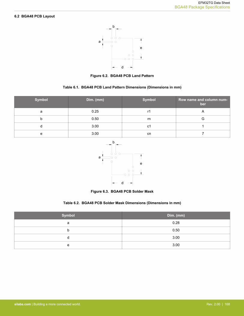
6.2 BGA48 PCB Layout
a
b
d
e
Figure 6.2. BGA48 PCB Land Pattern
Table 6.1. BGA48 PCB Land Pattern Dimensions (Dimensions in mm)
Symbol Dim. (mm) Symbol Row name and column num-ber
a 0.25 r1 A
b 0.50 rn G
d 3.00 c1 1
e 3.00 cn 7
a
b
d
e
Figure 6.3. BGA48 PCB Solder Mask
Table 6.2. BGA48 PCB Solder Mask Dimensions (Dimensions in mm)
Symbol Dim. (mm)
a 0.28
b 0.50
d 3.00
e 3.00
EFM32TG Data SheetBGA48 Package Specifications
silabs.com | Building a more connected world. Rev. 2.00 | 168
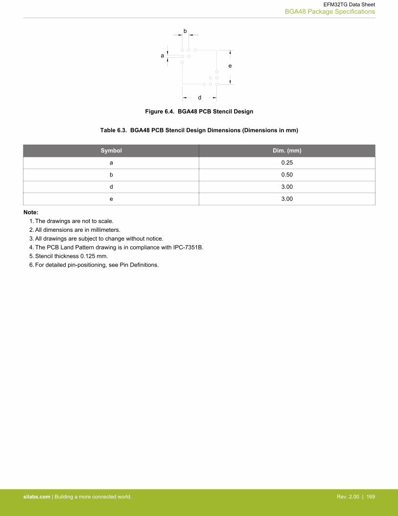
a
b
d
e
Figure 6.4. BGA48 PCB Stencil Design
Table 6.3. BGA48 PCB Stencil Design Dimensions (Dimensions in mm)
Symbol Dim. (mm)
a 0.25
b 0.50
d 3.00
e 3.00
Note:1. The drawings are not to scale.2. All dimensions are in millimeters.3. All drawings are subject to change without notice.4. The PCB Land Pattern drawing is in compliance with IPC-7351B.5. Stencil thickness 0.125 mm.6. For detailed pin-positioning, see Pin Definitions.
EFM32TG Data SheetBGA48 Package Specifications
silabs.com | Building a more connected world. Rev. 2.00 | 169

6.3 BGA48 Package Marking
In the illustration below package fields and position are shown.
Figure 6.5. Example Chip Marking (Top View)
EFM32TG Data SheetBGA48 Package Specifications
silabs.com | Building a more connected world. Rev. 2.00 | 170
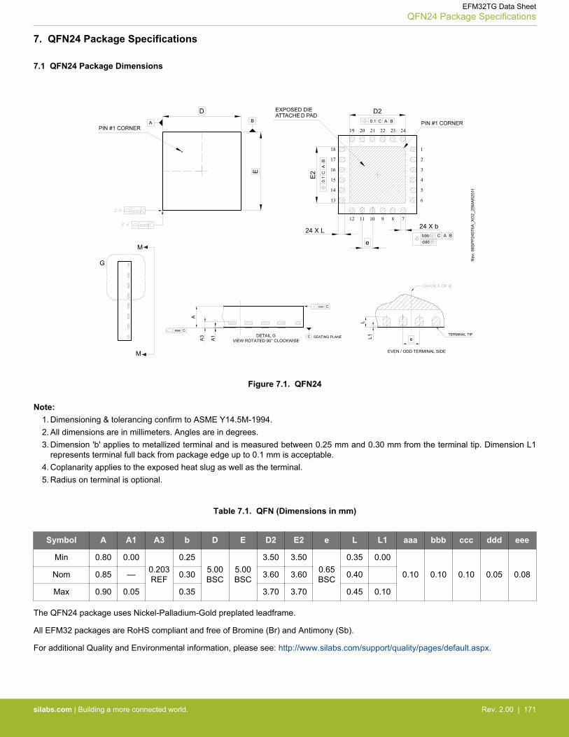
7. QFN24 Package Specifications
7.1 QFN24 Package Dimensions
Rev
: 98S
PP
2407
6A_X
O2_
25M
AR
2011
G
M
M
PIN #1 CORNER
D
E
D20.1 C A B
ATTACHE D PADEXPOSED DIE
e
PIN #1 CORNER
bbb C A Bddd
24 X b
E2
0.1
CA
B
1
A B
24 X L
2
3
4
5
6
18
17
16
15
14
13
789101112
242322212019
DETAIL GVIEW ROTATED 90° CLOCKWISE
EVEN / ODD TERMINAL SIDE
A3
A1
A
eee C
SEATING PLANEC
ccc C
eTERMINAL TIP
LL1
Figure 7.1. QFN24
Note:1. Dimensioning & tolerancing confirm to ASME Y14.5M-1994.2. All dimensions are in millimeters. Angles are in degrees.3. Dimension 'b' applies to metallized terminal and is measured between 0.25 mm and 0.30 mm from the terminal tip. Dimension L1
represents terminal full back from package edge up to 0.1 mm is acceptable.4. Coplanarity applies to the exposed heat slug as well as the terminal.5. Radius on terminal is optional.
Table 7.1. QFN (Dimensions in mm)
Symbol A A1 A3 b D E D2 E2 e L L1 aaa bbb ccc ddd eee
Min 0.80 0.000.203REF
0.255.00BSC
5.00BSC
3.50 3.500.65BSC
0.35 0.00
0.10 0.10 0.10 0.05 0.08Nom 0.85 — 0.30 3.60 3.60 0.40
Max 0.90 0.05 0.35 3.70 3.70 0.45 0.10
The QFN24 package uses Nickel-Palladium-Gold preplated leadframe.
All EFM32 packages are RoHS compliant and free of Bromine (Br) and Antimony (Sb).
For additional Quality and Environmental information, please see: http://www.silabs.com/support/quality/pages/default.aspx.
EFM32TG Data SheetQFN24 Package Specifications
silabs.com | Building a more connected world. Rev. 2.00 | 171
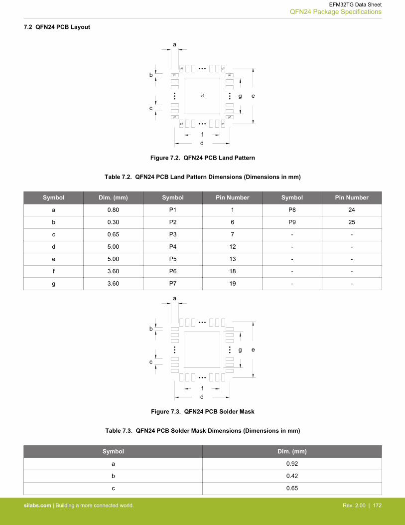
7.2 QFN24 PCB Layout
e
a
d
p1
p2
p3 p4
p5
p6
p7p8
c
b
p9
f
g
Figure 7.2. QFN24 PCB Land Pattern
Table 7.2. QFN24 PCB Land Pattern Dimensions (Dimensions in mm)
Symbol Dim. (mm) Symbol Pin Number Symbol Pin Number
a 0.80 P1 1 P8 24
b 0.30 P2 6 P9 25
c 0.65 P3 7 - -
d 5.00 P4 12 - -
e 5.00 P5 13 - -
f 3.60 P6 18 - -
g 3.60 P7 19 - -
e
a
d
c
b
f
g
Figure 7.3. QFN24 PCB Solder Mask
Table 7.3. QFN24 PCB Solder Mask Dimensions (Dimensions in mm)
Symbol Dim. (mm)
a 0.92
b 0.42
c 0.65
EFM32TG Data SheetQFN24 Package Specifications
silabs.com | Building a more connected world. Rev. 2.00 | 172
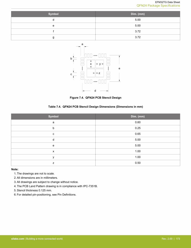
Symbol Dim. (mm)
d 5.00
e 5.00
f 3.72
g 3.72
e
a
d
c
b
x y
z
Figure 7.4. QFN24 PCB Stencil Design
Table 7.4. QFN24 PCB Stencil Design Dimensions (Dimensions in mm)
Symbol Dim. (mm)
a 0.60
b 0.25
c 0.65
d 5.00
e 5.00
x 1.00
y 1.00
z 0.50
Note:1. The drawings are not to scale.2. All dimensions are in millimeters.3. All drawings are subject to change without notice.4. The PCB Land Pattern drawing is in compliance with IPC-7351B.5. Stencil thickness 0.125 mm.6. For detailed pin-positioning, see Pin Definitions.
EFM32TG Data SheetQFN24 Package Specifications
silabs.com | Building a more connected world. Rev. 2.00 | 173
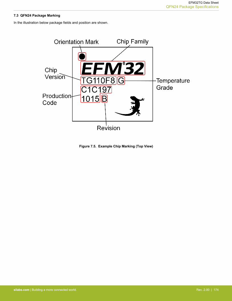
7.3 QFN24 Package Marking
In the illustration below package fields and position are shown.
Figure 7.5. Example Chip Marking (Top View)
EFM32TG Data SheetQFN24 Package Specifications
silabs.com | Building a more connected world. Rev. 2.00 | 174
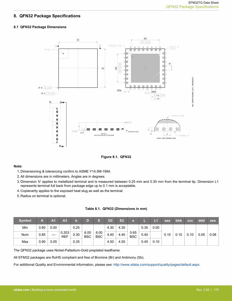
8. QFN32 Package Specifications
8.1 QFN32 Package Dimensions
Rev
: 98S
PP
3208
8A_X
O1_
10M
AR
2011
D
E
D2
32xL
E2
e
32xbm
m
MG
M
1
17
32
9
2
3
4
5
6
7
8
31302928272625
18
19
20
21
22
23
24
10111213141516
EVEN / ODD TERMINL SIDE
eL1
L
DETAIL GVIEW ROTATED 90° CLOCKWISE
A3
A
A1 SEATING PLANE
Figure 8.1. QFN32
Note:1. Dimensioning & tolerancing confirm to ASME Y14.5M-1994.2. All dimensions are in millimeters. Angles are in degrees.3. Dimension 'b' applies to metallized terminal and is measured between 0.25 mm and 0.30 mm from the terminal tip. Dimension L1
represents terminal full back from package edge up to 0.1 mm is acceptable.4. Coplanarity applies to the exposed heat slug as well as the terminal.5. Radius on terminal is optional.
Table 8.1. QFN32 (Dimensions in mm)
Symbol A A1 A3 b D E D2 E2 e L L1 aaa bbb ccc ddd eee
Min 0.80 0.000.203REF
0.256.00BSC
6.00BSC
4.30 4.300.65BSC
0.35 0.00
0.10 0.10 0.10 0.05 0.08Nom 0.85 — 0.30 4.40 4.40 0.40
Max 0.90 0.05 0.35 4.50 4.50 0.45 0.10
The QFN32 package uses Nickel-Palladium-Gold preplated leadframe.
All EFM32 packages are RoHS compliant and free of Bromine (Br) and Antimony (Sb).
For additional Quality and Environmental information, please see: http://www.silabs.com/support/quality/pages/default.aspx.
EFM32TG Data SheetQFN32 Package Specifications
silabs.com | Building a more connected world. Rev. 2.00 | 175
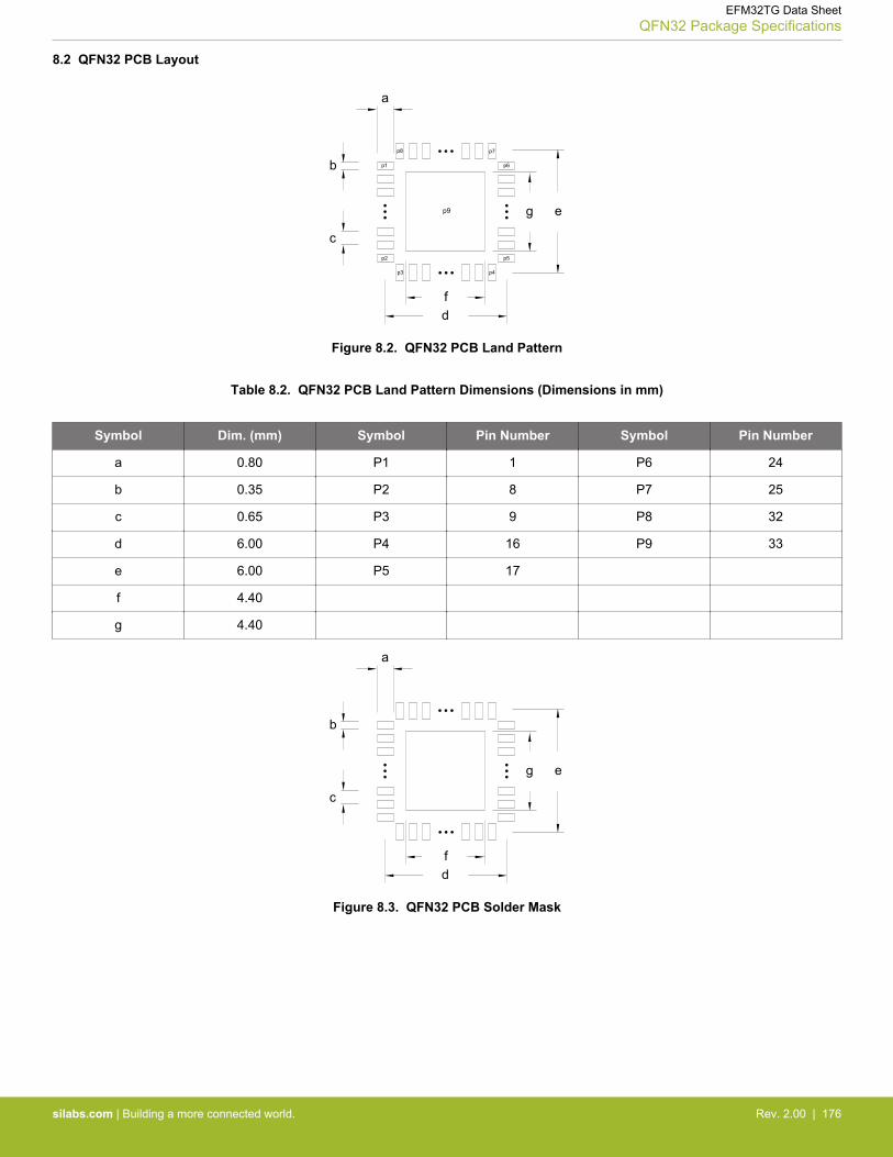
8.2 QFN32 PCB Layout
e
a
d
p1
p2
p3 p4
p5
p6
p7p8
c
b
p9
f
g
Figure 8.2. QFN32 PCB Land Pattern
Table 8.2. QFN32 PCB Land Pattern Dimensions (Dimensions in mm)
Symbol Dim. (mm) Symbol Pin Number Symbol Pin Number
a 0.80 P1 1 P6 24
b 0.35 P2 8 P7 25
c 0.65 P3 9 P8 32
d 6.00 P4 16 P9 33
e 6.00 P5 17
f 4.40
g 4.40
e
a
d
c
b
f
g
Figure 8.3. QFN32 PCB Solder Mask
EFM32TG Data SheetQFN32 Package Specifications
silabs.com | Building a more connected world. Rev. 2.00 | 176
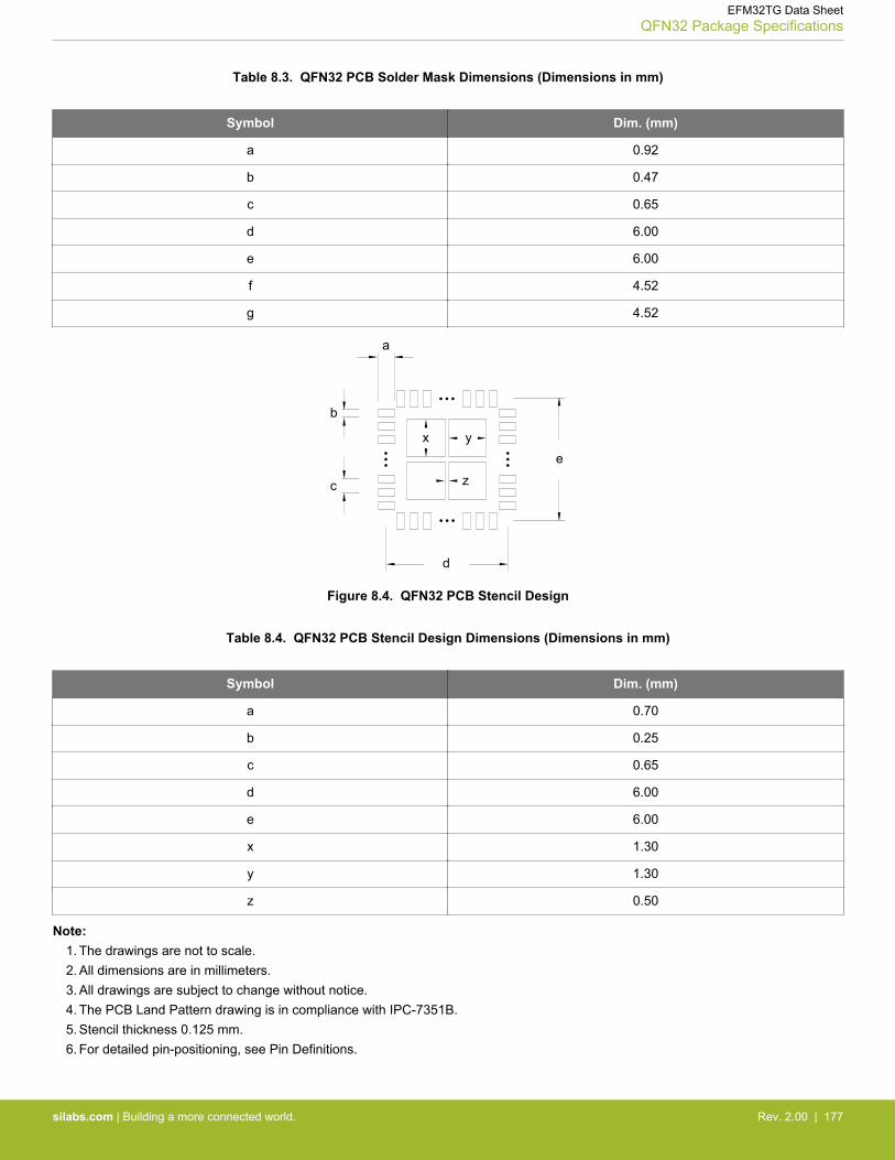
Table 8.3. QFN32 PCB Solder Mask Dimensions (Dimensions in mm)
Symbol Dim. (mm)
a 0.92
b 0.47
c 0.65
d 6.00
e 6.00
f 4.52
g 4.52
e
a
d
c
b
x y
z
Figure 8.4. QFN32 PCB Stencil Design
Table 8.4. QFN32 PCB Stencil Design Dimensions (Dimensions in mm)
Symbol Dim. (mm)
a 0.70
b 0.25
c 0.65
d 6.00
e 6.00
x 1.30
y 1.30
z 0.50
Note:1. The drawings are not to scale.2. All dimensions are in millimeters.3. All drawings are subject to change without notice.4. The PCB Land Pattern drawing is in compliance with IPC-7351B.5. Stencil thickness 0.125 mm.6. For detailed pin-positioning, see Pin Definitions.
EFM32TG Data SheetQFN32 Package Specifications
silabs.com | Building a more connected world. Rev. 2.00 | 177

8.3 QFN32 Package Marking
In the illustration below package fields and position are shown.
Figure 8.5. Example Chip Marking (Top View)
EFM32TG Data SheetQFN32 Package Specifications
silabs.com | Building a more connected world. Rev. 2.00 | 178
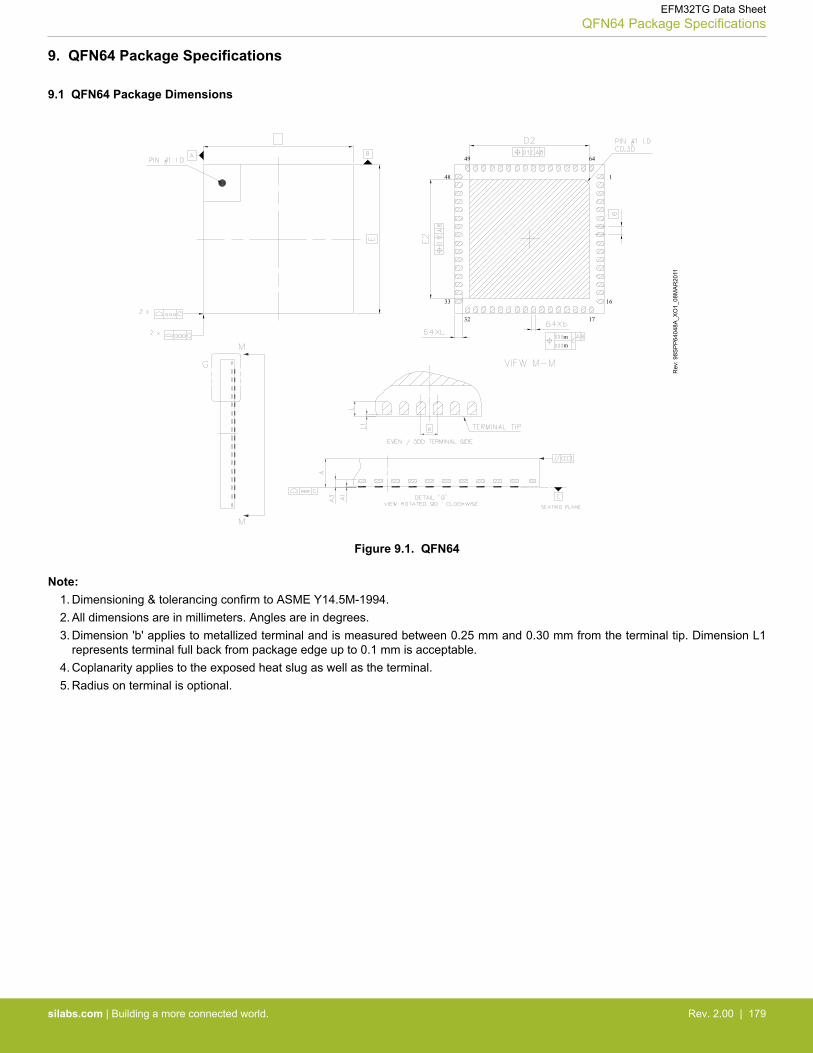
9. QFN64 Package Specifications
9.1 QFN64 Package Dimensions
Rev
: 98S
PP
6404
8A_X
O1_
08M
AR
2011
16
1732
33
64
1
49
48
m
m
Figure 9.1. QFN64
Note:1. Dimensioning & tolerancing confirm to ASME Y14.5M-1994.2. All dimensions are in millimeters. Angles are in degrees.3. Dimension 'b' applies to metallized terminal and is measured between 0.25 mm and 0.30 mm from the terminal tip. Dimension L1
represents terminal full back from package edge up to 0.1 mm is acceptable.4. Coplanarity applies to the exposed heat slug as well as the terminal.5. Radius on terminal is optional.
EFM32TG Data SheetQFN64 Package Specifications
silabs.com | Building a more connected world. Rev. 2.00 | 179
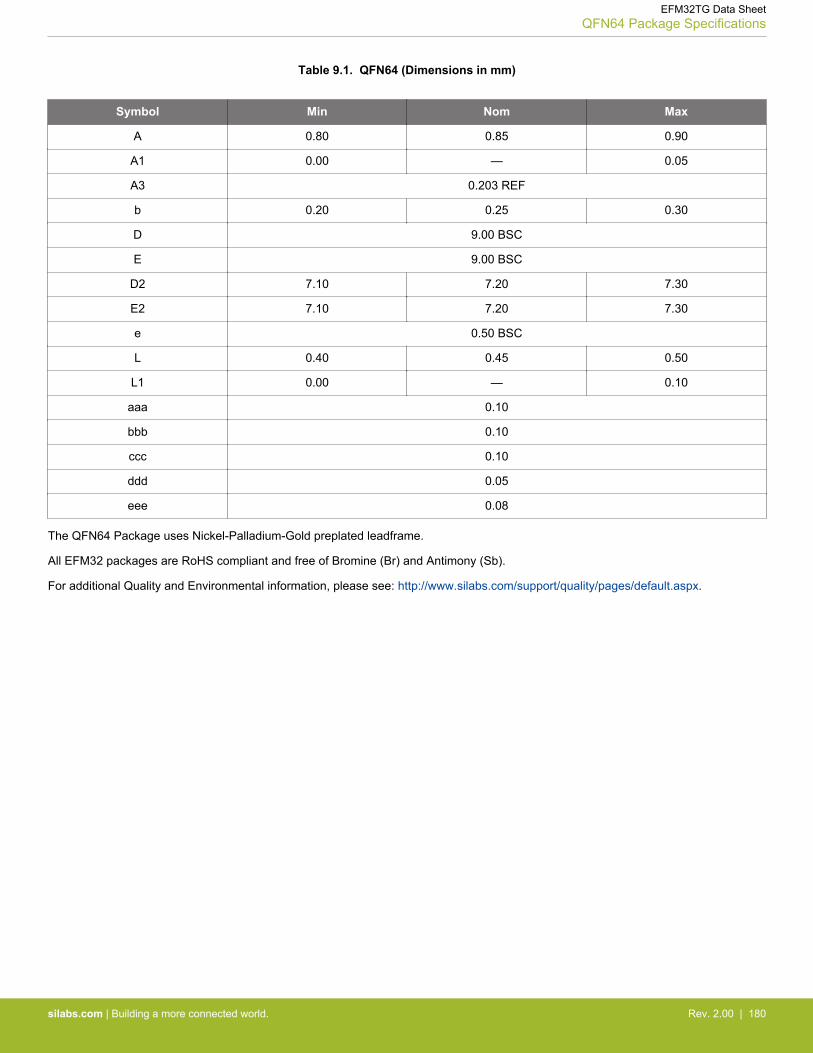
Table 9.1. QFN64 (Dimensions in mm)
Symbol Min Nom Max
A 0.80 0.85 0.90
A1 0.00 — 0.05
A3 0.203 REF
b 0.20 0.25 0.30
D 9.00 BSC
E 9.00 BSC
D2 7.10 7.20 7.30
E2 7.10 7.20 7.30
e 0.50 BSC
L 0.40 0.45 0.50
L1 0.00 — 0.10
aaa 0.10
bbb 0.10
ccc 0.10
ddd 0.05
eee 0.08
The QFN64 Package uses Nickel-Palladium-Gold preplated leadframe.
All EFM32 packages are RoHS compliant and free of Bromine (Br) and Antimony (Sb).
For additional Quality and Environmental information, please see: http://www.silabs.com/support/quality/pages/default.aspx.
EFM32TG Data SheetQFN64 Package Specifications
silabs.com | Building a more connected world. Rev. 2.00 | 180
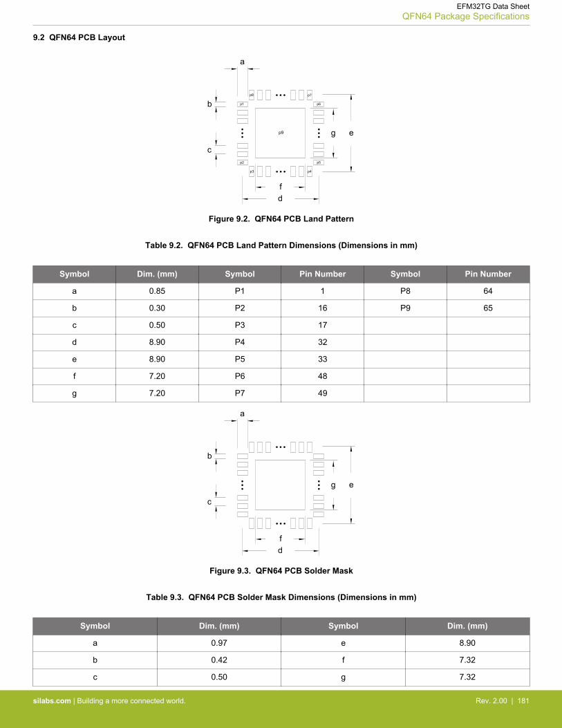
9.2 QFN64 PCB Layout
e
a
d
p1
p2
p3 p4
p5
p6
p7p8
c
b
p9
f
g
Figure 9.2. QFN64 PCB Land Pattern
Table 9.2. QFN64 PCB Land Pattern Dimensions (Dimensions in mm)
Symbol Dim. (mm) Symbol Pin Number Symbol Pin Number
a 0.85 P1 1 P8 64
b 0.30 P2 16 P9 65
c 0.50 P3 17
d 8.90 P4 32
e 8.90 P5 33
f 7.20 P6 48
g 7.20 P7 49
e
a
d
c
b
f
g
Figure 9.3. QFN64 PCB Solder Mask
Table 9.3. QFN64 PCB Solder Mask Dimensions (Dimensions in mm)
Symbol Dim. (mm) Symbol Dim. (mm)
a 0.97 e 8.90
b 0.42 f 7.32
c 0.50 g 7.32
EFM32TG Data SheetQFN64 Package Specifications
silabs.com | Building a more connected world. Rev. 2.00 | 181
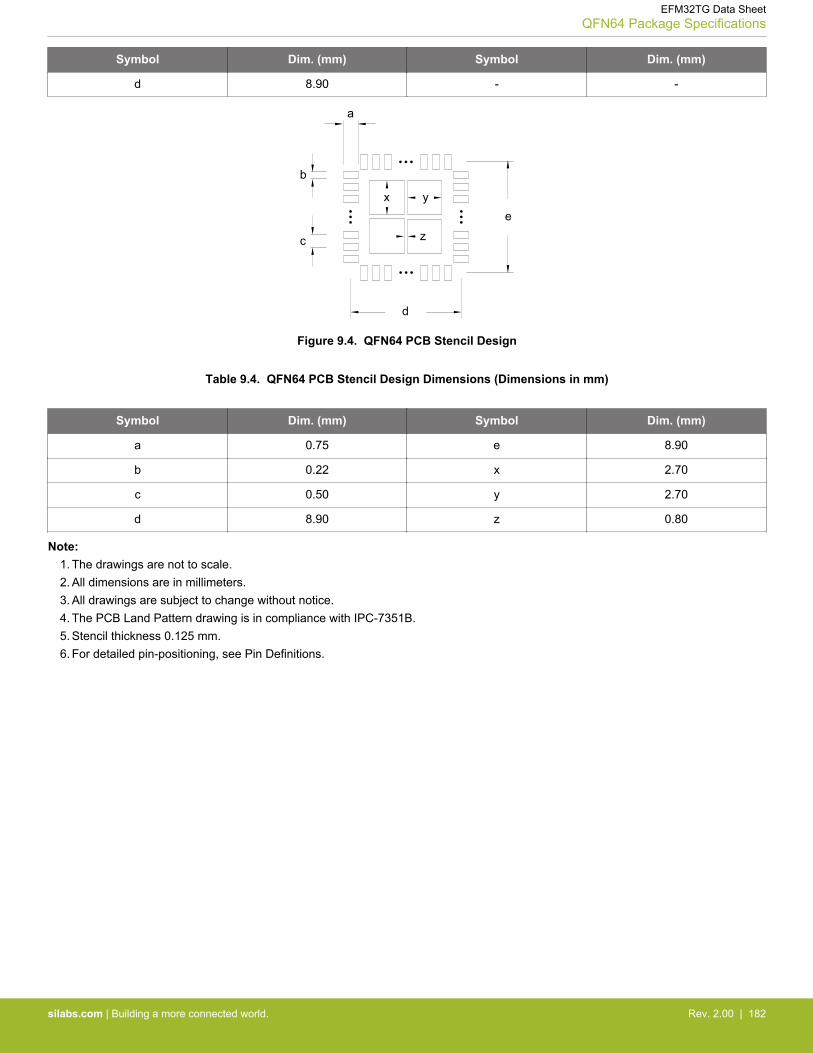
Symbol Dim. (mm) Symbol Dim. (mm)
d 8.90 - -
e
a
d
c
b
x y
z
Figure 9.4. QFN64 PCB Stencil Design
Table 9.4. QFN64 PCB Stencil Design Dimensions (Dimensions in mm)
Symbol Dim. (mm) Symbol Dim. (mm)
a 0.75 e 8.90
b 0.22 x 2.70
c 0.50 y 2.70
d 8.90 z 0.80
Note:1. The drawings are not to scale.2. All dimensions are in millimeters.3. All drawings are subject to change without notice.4. The PCB Land Pattern drawing is in compliance with IPC-7351B.5. Stencil thickness 0.125 mm.6. For detailed pin-positioning, see Pin Definitions.
EFM32TG Data SheetQFN64 Package Specifications
silabs.com | Building a more connected world. Rev. 2.00 | 182

9.3 QFN64 Package Marking
In the illustration below package fields and position are shown.
Figure 9.5. Example Chip Marking (Top View)
EFM32TG Data SheetQFN64 Package Specifications
silabs.com | Building a more connected world. Rev. 2.00 | 183
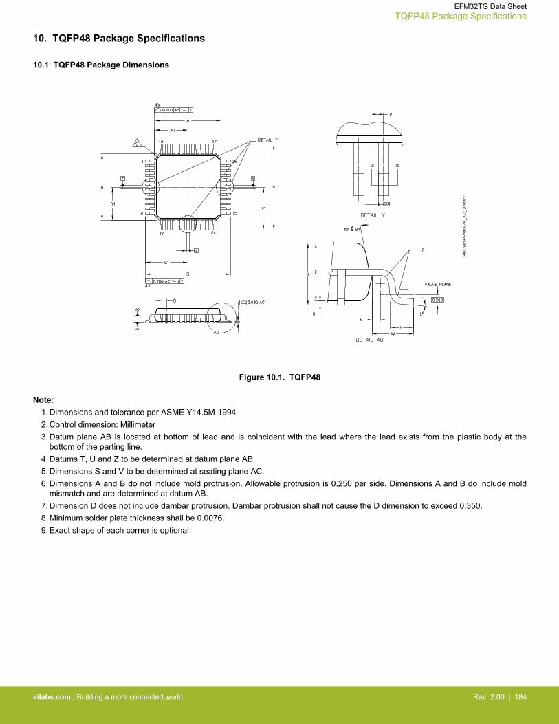
10. TQFP48 Package Specifications
10.1 TQFP48 Package Dimensions
Rev
: 98S
PP
4809
7A_X
O_3
0Mar
11
Figure 10.1. TQFP48
Note:1. Dimensions and tolerance per ASME Y14.5M-19942. Control dimension: Millimeter3. Datum plane AB is located at bottom of lead and is coincident with the lead where the lead exists from the plastic body at the
bottom of the parting line.4. Datums T, U and Z to be determined at datum plane AB.5. Dimensions S and V to be determined at seating plane AC.6. Dimensions A and B do not include mold protrusion. Allowable protrusion is 0.250 per side. Dimensions A and B do include mold
mismatch and are determined at datum AB.7. Dimension D does not include dambar protrusion. Dambar protrusion shall not cause the D dimension to exceed 0.350.8. Minimum solder plate thickness shall be 0.0076.9. Exact shape of each corner is optional.
EFM32TG Data SheetTQFP48 Package Specifications
silabs.com | Building a more connected world. Rev. 2.00 | 184
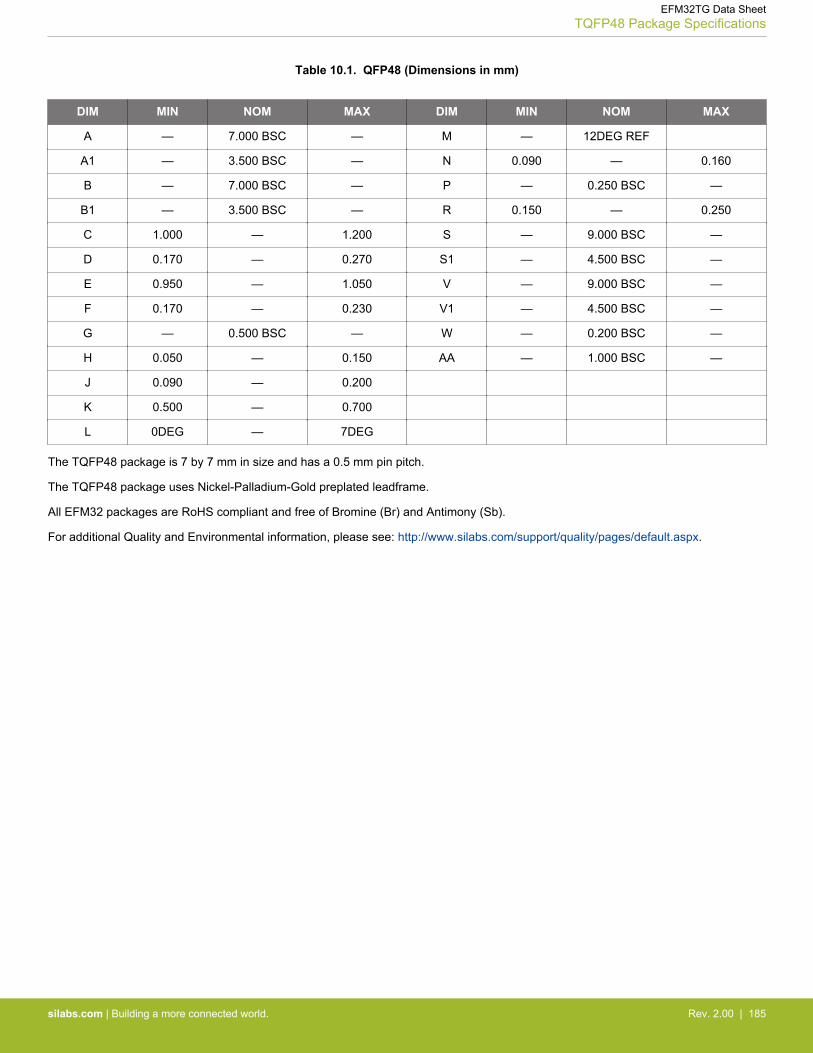
Table 10.1. QFP48 (Dimensions in mm)
DIM MIN NOM MAX DIM MIN NOM MAX
A — 7.000 BSC — M — 12DEG REF
A1 — 3.500 BSC — N 0.090 — 0.160
B — 7.000 BSC — P — 0.250 BSC —
B1 — 3.500 BSC — R 0.150 — 0.250
C 1.000 — 1.200 S — 9.000 BSC —
D 0.170 — 0.270 S1 — 4.500 BSC —
E 0.950 — 1.050 V — 9.000 BSC —
F 0.170 — 0.230 V1 — 4.500 BSC —
G — 0.500 BSC — W — 0.200 BSC —
H 0.050 — 0.150 AA — 1.000 BSC —
J 0.090 — 0.200
K 0.500 — 0.700
L 0DEG — 7DEG
The TQFP48 package is 7 by 7 mm in size and has a 0.5 mm pin pitch.
The TQFP48 package uses Nickel-Palladium-Gold preplated leadframe.
All EFM32 packages are RoHS compliant and free of Bromine (Br) and Antimony (Sb).
For additional Quality and Environmental information, please see: http://www.silabs.com/support/quality/pages/default.aspx.
EFM32TG Data SheetTQFP48 Package Specifications
silabs.com | Building a more connected world. Rev. 2.00 | 185
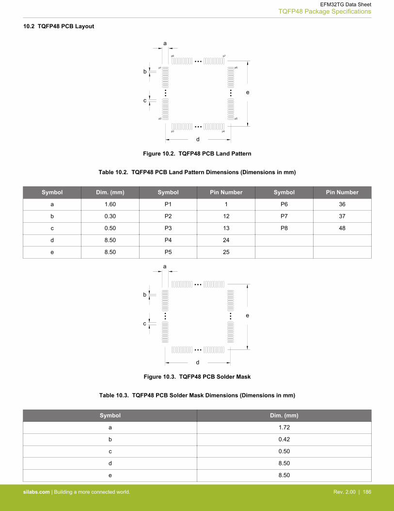
10.2 TQFP48 PCB Layout
e
a
d
c
bp1
p2
p3 p4
p5
p6
p7p8
Figure 10.2. TQFP48 PCB Land Pattern
Table 10.2. TQFP48 PCB Land Pattern Dimensions (Dimensions in mm)
Symbol Dim. (mm) Symbol Pin Number Symbol Pin Number
a 1.60 P1 1 P6 36
b 0.30 P2 12 P7 37
c 0.50 P3 13 P8 48
d 8.50 P4 24
e 8.50 P5 25
e
a
d
c
b
Figure 10.3. TQFP48 PCB Solder Mask
Table 10.3. TQFP48 PCB Solder Mask Dimensions (Dimensions in mm)
Symbol Dim. (mm)
a 1.72
b 0.42
c 0.50
d 8.50
e 8.50
EFM32TG Data SheetTQFP48 Package Specifications
silabs.com | Building a more connected world. Rev. 2.00 | 186
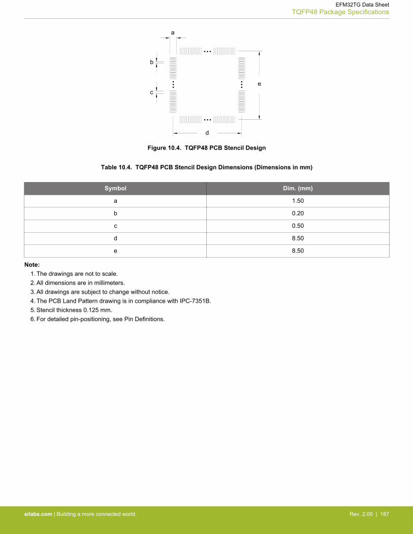
e
a
d
c
b
Figure 10.4. TQFP48 PCB Stencil Design
Table 10.4. TQFP48 PCB Stencil Design Dimensions (Dimensions in mm)
Symbol Dim. (mm)
a 1.50
b 0.20
c 0.50
d 8.50
e 8.50
Note:1. The drawings are not to scale.2. All dimensions are in millimeters.3. All drawings are subject to change without notice.4. The PCB Land Pattern drawing is in compliance with IPC-7351B.5. Stencil thickness 0.125 mm.6. For detailed pin-positioning, see Pin Definitions.
EFM32TG Data SheetTQFP48 Package Specifications
silabs.com | Building a more connected world. Rev. 2.00 | 187
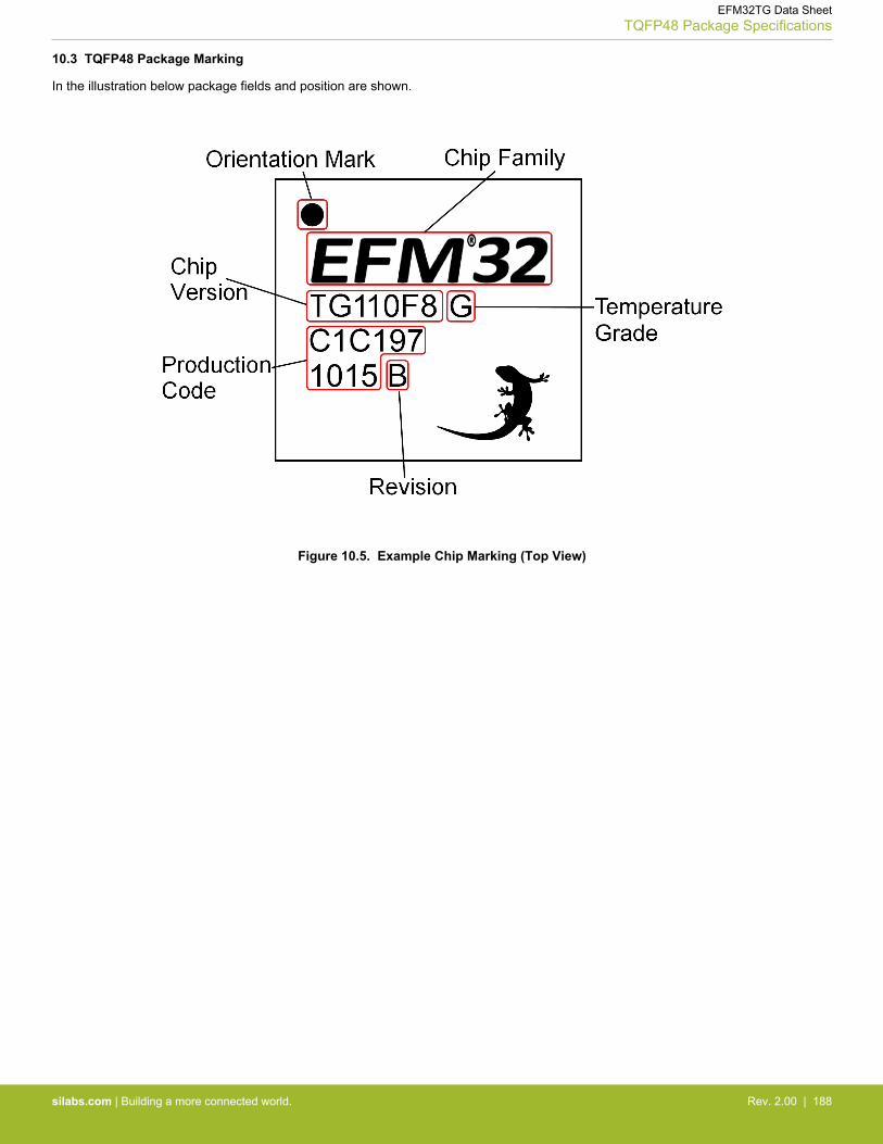
10.3 TQFP48 Package Marking
In the illustration below package fields and position are shown.
Figure 10.5. Example Chip Marking (Top View)
EFM32TG Data SheetTQFP48 Package Specifications
silabs.com | Building a more connected world. Rev. 2.00 | 188
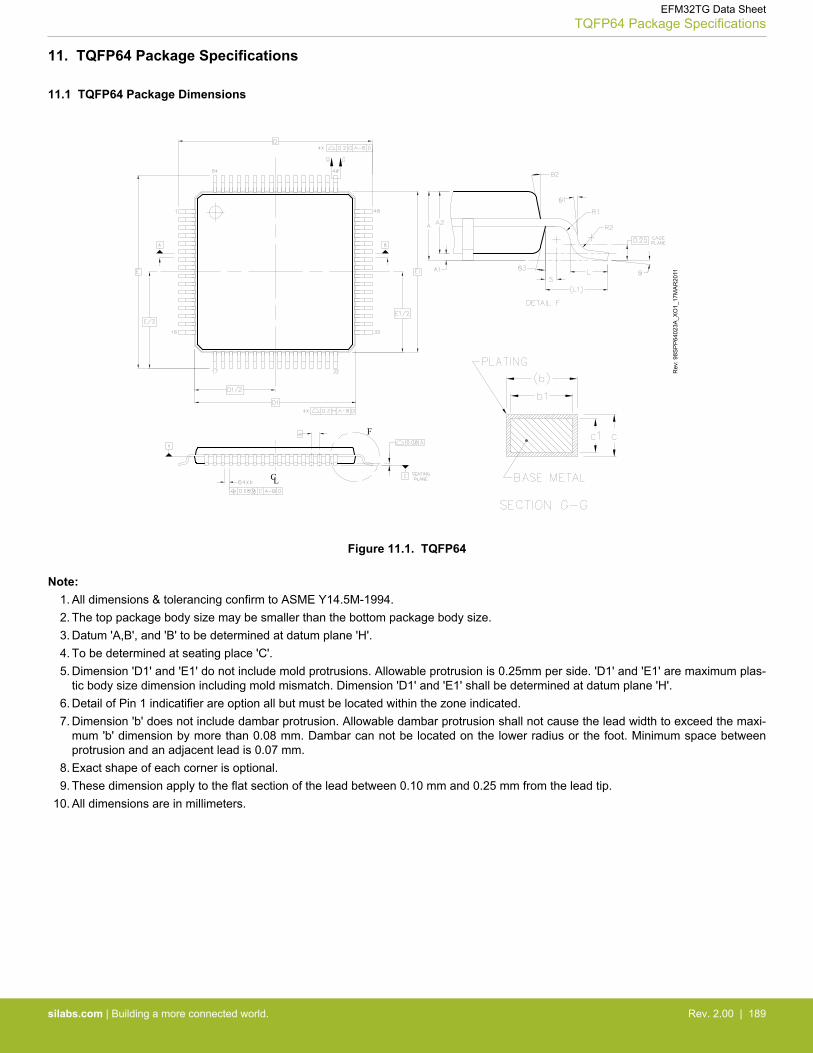
11. TQFP64 Package Specifications
11.1 TQFP64 Package Dimensions
Rev
: 98S
PP
6402
3A_X
O1_
17M
AR
2011
CL
F
Figure 11.1. TQFP64
Note:1. All dimensions & tolerancing confirm to ASME Y14.5M-1994.2. The top package body size may be smaller than the bottom package body size.3. Datum 'A,B', and 'B' to be determined at datum plane 'H'.4. To be determined at seating place 'C'.5. Dimension 'D1' and 'E1' do not include mold protrusions. Allowable protrusion is 0.25mm per side. 'D1' and 'E1' are maximum plas-
tic body size dimension including mold mismatch. Dimension 'D1' and 'E1' shall be determined at datum plane 'H'.6. Detail of Pin 1 indicatifier are option all but must be located within the zone indicated.7. Dimension 'b' does not include dambar protrusion. Allowable dambar protrusion shall not cause the lead width to exceed the maxi-
mum 'b' dimension by more than 0.08 mm. Dambar can not be located on the lower radius or the foot. Minimum space betweenprotrusion and an adjacent lead is 0.07 mm.
8. Exact shape of each corner is optional.9. These dimension apply to the flat section of the lead between 0.10 mm and 0.25 mm from the lead tip.
10. All dimensions are in millimeters.
EFM32TG Data SheetTQFP64 Package Specifications
silabs.com | Building a more connected world. Rev. 2.00 | 189
Table 11.1. QFP64 (Dimensions in mm)
DIM MIN NOM MAX DIM MIN NOM MAX
A — 1.10 1.20 L1 —
A1 0.05 — 0.15 R1 0.08 — —
A2 0.95 1.00 1.05 R2 0.08 — 0.20
b 0.17 0.22 0.27 S 0.20 — —
b1 0.17 0.20 0.23 θ 0° 3.5° 7°
c 0.09 — 0.20 θ1 0° — —
C1 0.09 — 0.16 θ2 11° 12° 13°
D 12.0 BSC θ3 11° 12° 13°
D1 10.0 BSC
e 0.50 BSC
E 12.0 BSC
E1 10.0 BSC
L 0.45 0.60 0.75
The TQFP64 Package is 10 by 10 mm in size and has a 0.5 mm pin pitch.
The TQFP64 Package uses Nickel-Palladium-Gold preplated leadframe.
All EFM32 packages are RoHS compliant and free of Bromine (Br) and Antimony (Sb).
For additional Quality and Environmental information, please see: http://www.silabs.com/support/quality/pages/default.aspx.
EFM32TG Data SheetTQFP64 Package Specifications
silabs.com | Building a more connected world. Rev. 2.00 | 190
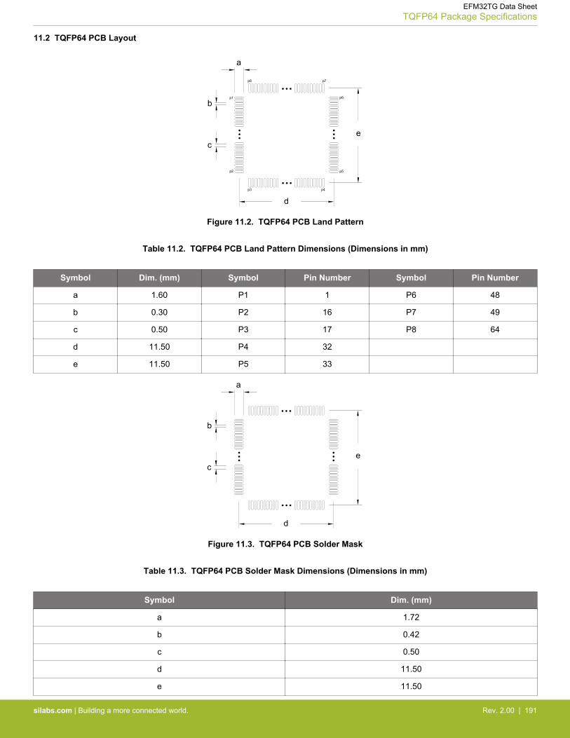
11.2 TQFP64 PCB Layout
e
a
d
c
bp1
p2
p3 p4
p5
p6
p7p8
Figure 11.2. TQFP64 PCB Land Pattern
Table 11.2. TQFP64 PCB Land Pattern Dimensions (Dimensions in mm)
Symbol Dim. (mm) Symbol Pin Number Symbol Pin Number
a 1.60 P1 1 P6 48
b 0.30 P2 16 P7 49
c 0.50 P3 17 P8 64
d 11.50 P4 32
e 11.50 P5 33
e
a
d
c
b
Figure 11.3. TQFP64 PCB Solder Mask
Table 11.3. TQFP64 PCB Solder Mask Dimensions (Dimensions in mm)
Symbol Dim. (mm)
a 1.72
b 0.42
c 0.50
d 11.50
e 11.50
EFM32TG Data SheetTQFP64 Package Specifications
silabs.com | Building a more connected world. Rev. 2.00 | 191

e
a
d
c
b
Figure 11.4. TQFP64 PCB Stencil Design
Table 11.4. TQFP64 PCB Stencil Design Dimensions (Dimensions in mm)
Symbol Dim. (mm)
a 1.50
b 0.20
c 0.50
d 11.50
e 11.50
Note:1. The drawings are not to scale.2. All dimensions are in millimeters.3. All drawings are subject to change without notice.4. The PCB Land Pattern drawing is in compliance with IPC-7351B.5. Stencil thickness 0.125 mm.6. For detailed pin-positioning, see Pin Definitions.
EFM32TG Data SheetTQFP64 Package Specifications
silabs.com | Building a more connected world. Rev. 2.00 | 192
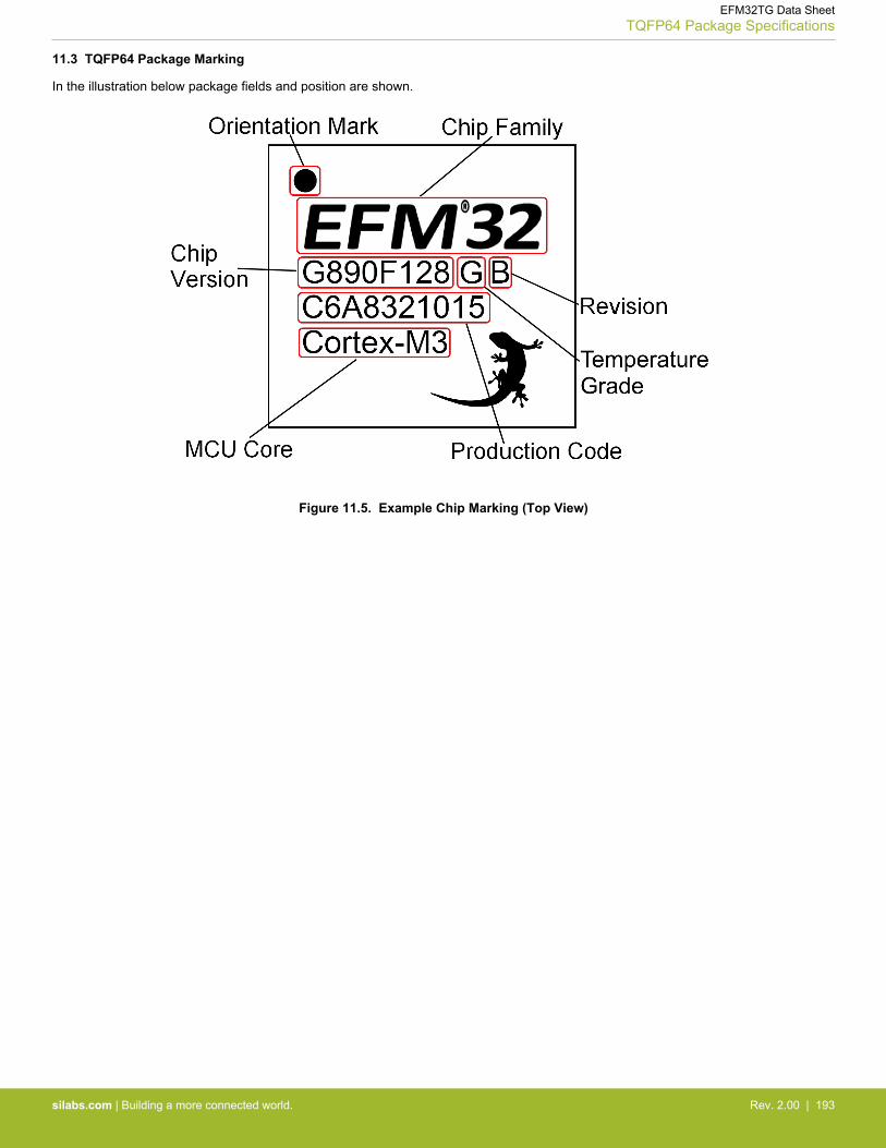
11.3 TQFP64 Package Marking
In the illustration below package fields and position are shown.
Figure 11.5. Example Chip Marking (Top View)
EFM32TG Data SheetTQFP64 Package Specifications
silabs.com | Building a more connected world. Rev. 2.00 | 193
12. Chip Revision, Solder Information, Errata
12.1 Chip Revision
The revision of a chip can be determined from the "Revision" field in the package marking.
12.2 Soldering Information
The latest IPC/JEDEC J-STD-020 recommendations for Pb-Free reflow soldering should be followed.
12.3 Errata
Please see the errata document for description and resolution of device errata. This document is available in Simplicity Studio and on-line at: http://www.silabs.com/support/pages/document-library.aspx?p=MCUs--32-bit
EFM32TG Data SheetChip Revision, Solder Information, Errata
silabs.com | Building a more connected world. Rev. 2.00 | 194
13. Revision History
13.1 Revision 2.00
August, 2018• Consolidated all EFM32TG data sheets:
• EFM32TG108• EFM32TG110• EFM32TG210• EFM32TG222• EFM32TG225• EFM32TG230• EFM32TG232• EFM32TG822• EFM32TG825• EFM32TG840• EFM32TG842
• Added a Feature List section.• 2. Ordering Information – Added ordering code decoder.• 3.3 Memory Map – Separated the Memory Map into two figures – one for core and code space listing and one for peripheral listing.• Environmental – Removed this section. Environmental specifications are available in the qualification report.• Removed MSL information (Moisture Sensitivity Level). Instead, MSL information can be found in the Qual report that is available on
the Silicon Labs website.• For QFN32 packages, corrected pin number for symbol P3.• 6.1 BGA48 Package Dimensions – Removed statements regarding materials used.• New formatting throughout.
EFM32TG Data SheetRevision History
silabs.com | Building a more connected world. Rev. 2.00 | 195
13.2 Revision 1.40
March 6th, 2015
This revision applies the following devices:• EFM32TG108• EFM32TG110• EFM32TG210• EFM32TG222• EFM32TG225• EFM32TG230• EFM32TG232• EFM32TG822• EFM32TG825• EFM32TG840• EFM32TG842
Updated Block Diagram.
Updated Energy Modes current consumption.
Updated Power Management section.
Updated LFRCO and HFRCO sections.
Added AUXHFRCO to block diagram and Electrical Characteristics.
Corrected unit to kHz on LFRCO plots y-axis.
For devices with ADC, updated ADC section and added clarification on conditions for INLADCand DNLADC parameters.
For devices with DAC, updated ADC section and added clarification on conditions for INLDACand DNLDAC parameters.
For devices with OPAMP, updated OPAMP section.
For devices with ACMP, updated ACMP section and the response time graph.
For devices with VCMP, updated VCMP section.
For QFN24 and QFN32 packages, updated Package dimensions table.
Updated Digital Peripherals section.
EFM32TG Data SheetRevision History
silabs.com | Building a more connected world. Rev. 2.00 | 196
13.3 Revision 1.30
July 2nd, 2014
This revision applies the following devices:• EFM32TG108• EFM32TG110• EFM32TG210• EFM32TG222• EFM32TG225• EFM32TG230• EFM32TG232• EFM32TG822• EFM32TG825• EFM32TG840• EFM32TG842
Updated current consumption.
Updated transition between energy modes.
Updated power management data.
Updated GPIO data.
Updated LFXO, HFXO, HFRCO and ULFRCO data.
Updated LFRCO and HFRCO plots.
Updated ACMP data.
13.4 Revision 1.21
November 21st, 2013
This revision applies the following devices:• EFM32TG108• EFM32TG110• EFM32TG210• EFM32TG222• EFM32TG225• EFM32TG230• EFM32TG232• EFM32TG822• EFM32TG825• EFM32TG840• EFM32TG842
Updated figures.
Updated errata-link.
Updated chip marking.
Added link to Environmental and Quality information.
For devices with DAC, re-added missing DAC-data.
EFM32TG Data SheetRevision History
silabs.com | Building a more connected world. Rev. 2.00 | 197
13.5 Revision 1.20
September 30th, 2013
This revision applies the following devices:• EFM32TG108• EFM32TG110• EFM32TG210• EFM32TG222• EFM32TG225• EFM32TG230• EFM32TG232• EFM32TG822• EFM32TG825• EFM32TG840• EFM32TG842
Added I2C characterization data.
For devices with DAC, corrected the DAC and OPAMP2 pin sharing information in the Alternate Functionality Pinout section.
Corrected GPIO operating voltage from 1.8 V to 1.85 V.
For devices with ADC, corrected the ADC gain and offset measurement reference voltage from 2.25 to 2.5V.
For devices with ADC, corrected the ADC resolution from 12, 10 and 6 bit to 12, 8 and 6 bit.
For QFP48 devices, updated the Max VESDCDM value to 750 V.
Document changed status from "Preliminary".
Updated Environmental information.
Updated trademark, disclaimer and contact information.
Other minor corrections.
13.6 Revision 1.10
June 28th, 2013
This revision applies the following devices:• EFM32TG108• EFM32TG110• EFM32TG210• EFM32TG222• EFM32TG225• EFM32TG230• EFM32TG232• EFM32TG822• EFM32TG825• EFM32TG840• EFM32TG842
For BGA packages, updated PCB Land Pattern, PCB Solder Mask and PCB Stencil Design figures.
Updated power requirements in the Power Management section.
Removed minimum load capacitance figure and table. Added reference to application note.
Other minor corrections.
EFM32TG Data SheetRevision History
silabs.com | Building a more connected world. Rev. 2.00 | 198
13.7 Revision 1.00
September 11th, 2012
This revision applies the following devices:• EFM32TG108• EFM32TG110• EFM32TG210• EFM32TG222• EFM32TG225• EFM32TG230• EFM32TG232• EFM32TG822• EFM32TG825• EFM32TG840• EFM32TG842
Updated the HFRCO 1 MHz band typical value to 1.2 MHz.
Updated the HFRCO 7 MHz band typical value to 6.6 MHz.
Added GPIO_EM4WU3, GPIO_EM4WU4 and GPIO_EM4WU5 pins and removed GPIO_EM4WU1 in the Alternate functionality over-view table.
Other minor corrections.
13.8 Revision 0.96
May 4th, 2012
This revision applies the following devices:• EFM32TG108• EFM32TG110• EFM32TG210• EFM32TG222• EFM32TG225• EFM32TG230• EFM32TG232• EFM32TG822• EFM32TG825• EFM32TG840• EFM32TG842
For BGA48 packages, added PCB land pattern, Stencil design and solder mask.
For BGA48 packages, corrected PCB footprint figures and tables.
EFM32TG Data SheetRevision History
silabs.com | Building a more connected world. Rev. 2.00 | 199
13.9 Revision 0.95
February 27th, 2012
This revision applies the following devices:• EFM32TG108• EFM32TG110• EFM32TG210• EFM32TG222• EFM32TG225• EFM32TG230• EFM32TG232• EFM32TG822• EFM32TG825• EFM32TG840• EFM32TG842
For BGA48 packages, initial preliminary release.
For BGA48 packages, corrected operating voltage from 1.8 V to 1.85 V.
For BGA48 packages, added rising POR level and corrected Thermometer output gradient in Electrical Characteristics section.
For BGA48 packages, updated Minimum Load Capacitance (CLFXOL) Requirement For Safe Crystal Startup.
For BGA48 packages, added Gain error drift and Offset error drift to ADC table.
For devices with OPAMP in BGA48 packages, added Opamp pinout overview.
For BGA48 packages, added reference to errata document.
13.10 Revision 0.92
July 22nd, 2011
This revision applies the following devices:• EFM32TG108• EFM32TG110• EFM32TG210• EFM32TG222• EFM32TG225• EFM32TG230• EFM32TG232• EFM32TG822• EFM32TG825• EFM32TG840• EFM32TG842
Updated current consumption numbers from latest device characterization data.
For devices with OPAMP, updated OPAMP electrical characteristics.
For devices with ADC, made ADC plots render properly in Adobe Reader.
For EFM32TG822, corrected number of DAC channels available.
For EFM32TG232, corrected number of DAC channels available.
For EFM32TG842, corrected number of DAC channels available.
For EFM32TG230, corrected number of DAC channels available.
EFM32TG Data SheetRevision History
silabs.com | Building a more connected world. Rev. 2.00 | 200
13.11 Revision 0.91
February 4th, 2011
This revision applies the following devices:• EFM32TG108• EFM32TG110• EFM32TG210• EFM32TG230• EFM32TG840
Corrected max DAC sampling rate.
Increased max storage temperature.
Added data for <150°C and <70°C on Flash data retention.
Changed latch-up sensitivity test description.
Added IO leakage current.
Added Flash current consumption.
Updated HFRCO data.
Updated LFRCO data.
For devices with ADC, added graph for ADC Absolute Offset over temperature.
For devices with ADC, added graph for ADC Temperature sensor readout.
For devices with OPAMP, updated OPAMP electrical characteristics.
13.12 Revision 0.90
December 1st, 2010
This revision applies the following devices:• EFM32TG108• EFM32TG110• EFM32TG210• EFM32TG230• EFM32TG840
New peripherals added to pinout, including LESENSE and OpAmps.
April 14th, 2011
This revision applies the following devices:• EFM32TG222• EFM32TG232• EFM32TG822
Initial preliminary release.
June 30th, 2011
This revision applies the following devices:• EFM32TG842
Initial preliminary release.
EFM32TG Data SheetRevision History
silabs.com | Building a more connected world. Rev. 2.00 | 201
13.13 Revision 0.70
August 16th, 2010
This revision applies the following devices:• EFM32TG110
Added pinout.
13.14 Revision 0.60
June 8th, 2010
This revision applies the following devices:• EFM32TG230
Corrected pinout.
13.15 Revision 0.50
May 25th, 2010
This revision applies the following devices:• EFM32TG108• EFM32TG110• EFM32TG210• EFM32TG230• EFM32TG840
Block diagram update.
13.16 Revision 0.40
March 26th, 2010
This revision applies the following devices:• EFM32TG108• EFM32TG110• EFM32TG210• EFM32TG230• EFM32TG840
Initial preliminary release.
EFM32TG Data SheetRevision History
silabs.com | Building a more connected world. Rev. 2.00 | 202

http://www.silabs.com
Silicon Laboratories Inc.400 West Cesar ChavezAustin, TX 78701USA
Simplicity StudioOne-click access to MCU and wireless tools, documentation, software, source code libraries & more. Available for Windows, Mac and Linux!
IoT Portfoliowww.silabs.com/IoT
SW/HWwww.silabs.com/simplicity
Qualitywww.silabs.com/quality
Support and Communitycommunity.silabs.com
DisclaimerSilicon Labs intends to provide customers with the latest, accurate, and in-depth documentation of all peripherals and modules available for system and software implementers using or intending to use the Silicon Labs products. Characterization data, available modules and peripherals, memory sizes and memory addresses refer to each specific device, and "Typical" parameters provided can and do vary in different applications. Application examples described herein are for illustrative purposes only. Silicon Labs reserves the right to make changes without further notice and limitation to product information, specifications, and descriptions herein, and does not give warranties as to the accuracy or completeness of the included information. Silicon Labs shall have no liability for the consequences of use of the information supplied herein. This document does not imply or express copyright licenses granted hereunder to design or fabricate any integrated circuits. The products are not designed or authorized to be used within any Life Support System without the specific written consent of Silicon Labs. A "Life Support System" is any product or system intended to support or sustain life and/or health, which, if it fails, can be reasonably expected to result in significant personal injury or death. Silicon Labs products are not designed or authorized for military applications. Silicon Labs products shall under no circumstances be used in weapons of mass destruction including (but not limited to) nuclear, biological or chemical weapons, or missiles capable of delivering such weapons.
Trademark InformationSilicon Laboratories Inc.® , Silicon Laboratories®, Silicon Labs®, SiLabs® and the Silicon Labs logo®, Bluegiga®, Bluegiga Logo®, Clockbuilder®, CMEMS®, DSPLL®, EFM®, EFM32®, EFR, Ember®, Energy Micro, Energy Micro logo and combinations thereof, "the world’s most energy friendly microcontrollers", Ember®, EZLink®, EZRadio®, EZRadioPRO®, Gecko®, ISOmodem®, Micrium, Precision32®, ProSLIC®, Simplicity Studio®, SiPHY®, Telegesis, the Telegesis Logo®, USBXpress®, Zentri, Z-Wave, and others are trademarks or registered trademarks of Silicon Labs. ARM, CORTEX, Cortex-M3 and THUMB are trademarks or registered trademarks of ARM Holdings. Keil is a registered trademark of ARM Limited. All other products or brand names mentioned herein are trademarks of their respective holders.