1. Introduction 2. Placement - IC Plus Note/IP101A layout guidelines... · RJ45 Magnetic IP101 MII...
6
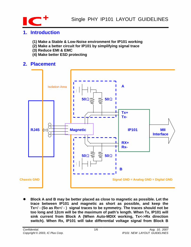
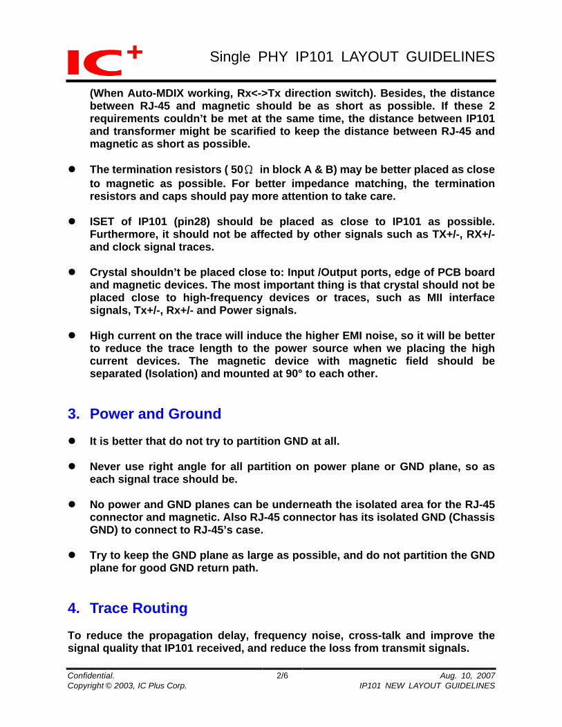
Single PHY IP101 LAYOUT GUIDELINES Confidential. 1. Introduction (1) Make a Stable & Low-Noise environment for IP101 working (2) Make a better circuit for IP101 by simplifying signal trace (3) Reduce EMI & EMC (4) Make better ESD protecting 2. Placement 1/6 Aug. 10, 2007 Copyright © 2003, IC Plus Corp. IP101 NEW LAYOUT GUIDELINES A 50Ω 50Ω Tx+ Tx- RJ45 Magnetic IP101 MII Interface RX+ Rx- 50Ω 50Ω B Isolation Area Chassis GND Signal GND = Analog GND = Digital GND z Block A and B may be better placed as close to magnetic as possible. Let the trace between IP101 and magnetic as short as possible, and keep the Tx+/-(So as Rx+/-) signal traces to be symmetry. The traces should not be too long and 12cm will be the maximum of path’s length. When Tx, IP101 will sink current from Block A (When Auto-MDIX working, Tx<->Rx direction switch). When Rx, IP101 will take differential voltage signal from Block B
-
Upload
nguyenphuc -
Category
Documents
-
view
218 -
download
6
Transcript of 1. Introduction 2. Placement - IC Plus Note/IP101A layout guidelines... · RJ45 Magnetic IP101 MII...
Single PHY IP101 LAYOUT GUIDELINES
Confidential.
1. Introduction
(1) Make a Stable & Low-Noise environment for IP101 working (2) Make a better circuit for IP101 by simplifying signal trace (3) Reduce EMI & EMC (4) Make better ESD protecting
2. Placement
1/6 Aug. 10, 2007Copyright © 2003, IC Plus Corp. IP101 NEW LAYOUT GUIDELINES
A 50Ω 50Ω Tx+ Tx- RJ45 Magnetic IP101 MII Interface RX+ Rx- 50Ω 50Ω B
Isolation Area
Chassis GND Signal GND = Analog GND = Digital GND
Block A and B may be better placed as close to magnetic as possible. Let the
trace between IP101 and magnetic as short as possible, and keep the Tx+/-(So as Rx+/-) signal traces to be symmetry. The traces should not be too long and 12cm will be the maximum of path’s length. When Tx, IP101 will sink current from Block A (When Auto-MDIX working, Tx<->Rx direction switch). When Rx, IP101 will take differential voltage signal from Block B
Single PHY IP101 LAYOUT GUIDELINES
Confidential. 2/6 Aug. 10, 2007Copyright © 2003, IC Plus Corp. IP101 NEW LAYOUT GUIDELINES
(When Auto-MDIX working, Rx<->Tx direction switch). Besides, the distance between RJ-45 and magnetic should be as short as possible. If these 2 requirements couldn’t be met at the same time, the distance between IP101 and transformer might be scarified to keep the distance between RJ-45 and magnetic as short as possible.
The termination resistors ( 50Ω in block A & B) may be better placed as close
to magnetic as possible. For better impedance matching, the termination resistors and caps should pay more attention to take care.
ISET of IP101 (pin28) should be placed as close to IP101 as possible.
Furthermore, it should not be affected by other signals such as TX+/-, RX+/- and clock signal traces.
Crystal shouldn’t be placed close to: Input /Output ports, edge of PCB board
and magnetic devices. The most important thing is that crystal should not be placed close to high-frequency devices or traces, such as MII interface signals, Tx+/-, Rx+/- and Power signals.
High current on the trace will induce the higher EMI noise, so it will be better
to reduce the trace length to the power source when we placing the high current devices. The magnetic device with magnetic field should be separated (Isolation) and mounted at 90° to each other.
3. Power and Ground It is better that do not try to partition GND at all.
Never use right angle for all partition on power plane or GND plane, so as
each signal trace should be. No power and GND planes can be underneath the isolated area for the RJ-45
connector and magnetic. Also RJ-45 connector has its isolated GND (Chassis GND) to connect to RJ-45’s case.
Try to keep the GND plane as large as possible, and do not partition the GND
plane for good GND return path. 4. Trace Routing To reduce the propagation delay, frequency noise, cross-talk and improve the signal quality that IP101 received, and reduce the loss from transmit signals.
Single PHY IP101 LAYOUT GUIDELINES
Confidential.
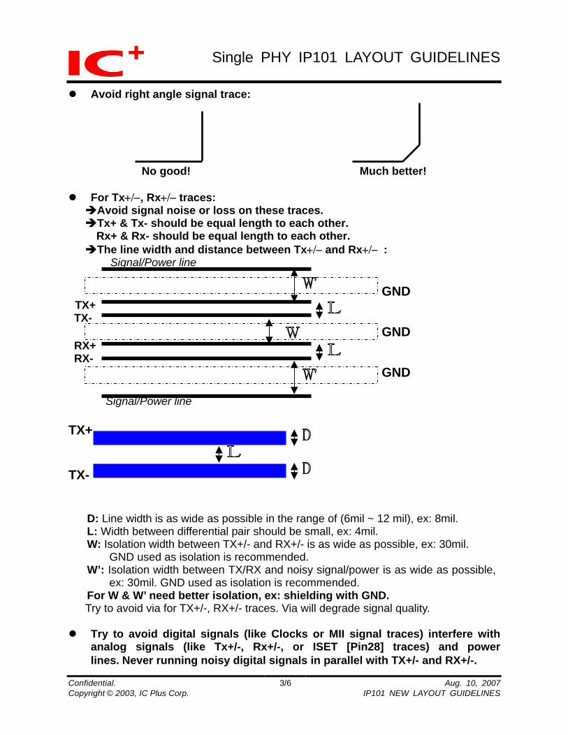
Avoid right angle signal trace:
3/6 Aug. 10, 2007Copyright © 2003, IC Plus Corp. IP101 NEW LAYOUT GUIDELINES
No good! Much better! For Tx+/−, Rx+/− traces:
Avoid signal noise or loss on these traces. Tx+ & Tx- should be equal length to each other. Rx+ & Rx- should be equal length to each other. The line width and distance between Tx+/− and Rx+/− :
Signal/Power line
GND TX+ TX- GND RX+ RX- GND Signal/Power line TX+ TX-
D: Line width is as wide as possible in the range of (6mil ~ 12 mil), ex: 8mil. L: Width between differential pair should be small, ex: 4mil. W: Isolation width between TX+/- and RX+/- is as wide as possible, ex: 30mil.
GND used as isolation is recommended. W’: Isolation width between TX/RX and noisy signal/power is as wide as possible,
ex: 30mil. GND used as isolation is recommended. For W & W’ need better isolation, ex: shielding with GND.
Try to avoid via for TX+/-, RX+/- traces. Via will degrade signal quality. Try to avoid digital signals (like Clocks or MII signal traces) interfere with
analog signals (like Tx+/-, Rx+/-, or ISET [Pin28] traces) and power lines. Never running noisy digital signals in parallel with TX+/- and RX+/-.
Single PHY IP101 LAYOUT GUIDELINES
Confidential.
The traces of power, ground, and those need de-couple cap should be
shorter and wider. If vias are not eliminated on the trace for de-couple cap, try to enlarge the diameter of these vias.
For some critical signals, clock and the other high speed signal traces should
be as short and wide as possible. (Surely that is compared with normal signal traces.) And it’s better having the GND plane under them, and it is even better with the GND plane around it.
The length of each signal trace shouldn’t exceed 1/20 of the highest harmonic
wavelength. For example, for the 25M clock trace shouldn’t exceed 30cm and for the 125M signal trace shouldn’t exceed 12cm (Tx+/-, Rx+/-).
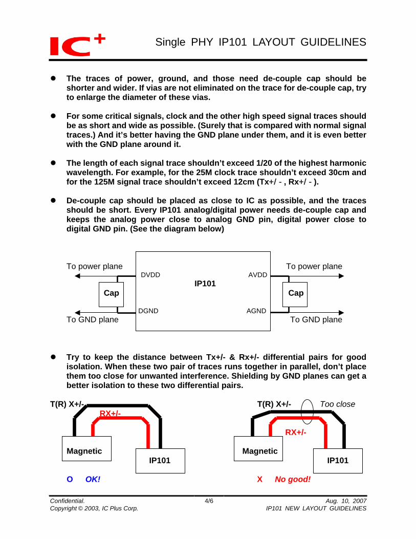
De-couple cap should be placed as close to IC as possible, and the traces
should be short. Every IP101 analog/digital power needs de-couple cap and keeps the analog power close to analog GND pin, digital power close to digital GND pin. (See the diagram below)
To power plane To power plane DVDD AVDD IP101 Cap Cap
4/6 Aug. 10, 2007Copyright © 2003, IC Plus Corp. IP101 NEW LAYOUT GUIDELINES
DGND AGND To GND plane To GND plane Try to keep the distance between Tx+/- & Rx+/- differential pairs for good
isolation. When these two pair of traces runs together in parallel, don’t place them too close for unwanted interference. Shielding by GND planes can get a better isolation to these two differential pairs.
T(R) X+/- T(R) X+/- Too close RX+/- RX+/- Magnetic Magnetic IP101 IP101 O OK! X No good!
Single PHY IP101 LAYOUT GUIDELINES
Confidential. 5/6 Aug. 10, 2007Copyright © 2003, IC Plus Corp. IP101 NEW LAYOUT GUIDELINES
The signal trace length difference between Tx+ and Tx- (Same as Rx+ and Rx-) should be kept as small as possible, better within 1 inch.
Ferrite Beads should be as close to IC pins and let it on the rating of
100Ω@100MHz
The ferrite bead between DVDD and AVDD of IP101A pins should be placed as close to IP101A as possible, and at the same side as IP101A, not opposite side.
The ferrite bead between Regout and RegIn of IP101A pins should be placed
as close to IP101A as possible, and at the same side as IP101A, not opposite side.
Magnetic: Any Magnetic with Tx/Rx turn ration of 1:1/1:1 are suitable for P101,
such as SINKA LS518/LS502, Bothhand TS8121C/TS6121C. Transformer supporting automdix function is recommended for better EMI performance.
5. Better Analog Performance When using regulator such as 5V -> 3.3V, the rated current of the regulator
should be at least 300mA. Both Analog GND pins (29,35) and Digital GND pins (11,17,45) must maintain
a good GND return path (One GND plane is recommended. Avoid using single ended GND or making the GND plane discrete. Keep the circuit’s return path back to the system’s real GND as short as possible. This is especially important for 2 layers PCB layout.
When using 25MHz crystal as IP101’s clock source, the spec of crystal is better under 50ppm, please refer to the attached crystal’s spec. Two caps attached to X1 (Pin46) and X2 (Pin47) should be close to 20pF.
Avoid placing cap in the clock path when using oscillator as clock source.
If EMI of the system couldn’t pass, add some de-couple caps (such as 0.1uF,
10nF, 1nF, 390pF..etc) between systems Power to GND. 6. ESD Protecting
Single PHY IP101 LAYOUT GUIDELINES
Confidential.
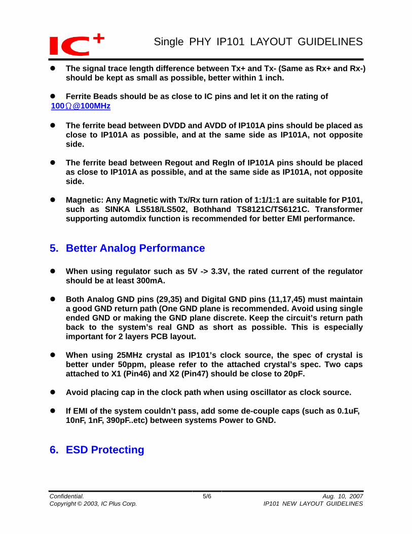
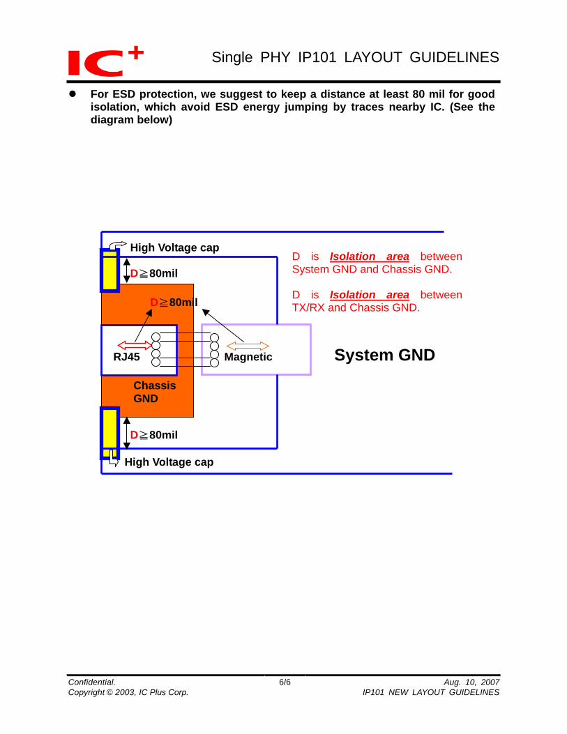
For ESD protection, we suggest to keep a distance at least 80 mil for good isolation, which avoid ESD energy jumping by traces nearby IC. (See the diagram below)
6/6 Aug. 10, 2007Copyright © 2003, IC Plus Corp. IP101 NEW LAYOUT GUIDELINES
High Voltage cap D≧80mil RJ45 Magnetic System GND D≧80mil High Voltage cap
D is Isolation area between System GND and Chassis GND. D is Isolation area between TX/RX and Chassis GND.
Chassis GND
D≧80mil