
![Fabrication of CdS/SnS Heterojunction for Photovoltaic ...file.scirp.org/pdf/WJCMP_2015012113550782.pdf · R. Reddy [4] improved the ... SnS thin films were deposited on the CdS layers](https://static.fdocument.org/doc/165x107/5aa49b0b7f8b9afa758c254b/fabrication-of-cdssns-heterojunction-for-photovoltaic-filescirporgpdfwjcmp.jpg)
γλώσσες
Σελίδες
Νομικός

Study of electrical and micro-structural properties of high-j gatedielectric stacks deposited using pulse laser deposition for MOScapacitor applications
A. Srivastava • O. Mangla • R. K. Nahar •
V. Gupta • C. K. Sarkar
Received: 9 March 2014 / Accepted: 12 May 2014
� Springer Science+Business Media New York 2014
Abstract The electrical properties of hafnium oxide
(HfO2) gate dielectric as a metal–oxide–semiconductor
(MOS) capacitor structure deposited using pulse laser
deposition (PLD) technique at optimum substrate temper-
atures in an oxygen ambient gas are investigated. The film
thickness and microstructure are examined using ellips-
ometer and atomic force microscope (AFM), respectively
to see the effect of substrate temperatures on the device
properties. The electrical J–V, C–V characteristics of the
dielectric films are investigated employing Al–HfO2–Si
MOS capacitor structure. The important parameters like
leakage current density, flat-band voltage (Vfb) and oxide-
charge density (Qox) for MOS capacitors are extracted and
investigated for optimum substrate temperature. Further,
electrical studies of these MOS capacitors have been car-
ried out by incorporating La2O3 into HfO2 to fabricate
HfO2/La2O3 dielectric stacks at an optimized substrate
temperature of 800 �C using a PLD deposition technique
under oxygen ambient. These Al–HfO2–La2O3–Si
dielectric stacks MOS capacitor structure are found to
possess better electrical properties than that of HfO2 based
MOS capacitors using the PLD deposition technique.
1 Introduction
Silicon dioxide (SiO2) was a preferred gate dielectric
material in metal–oxide–semiconductor (MOS) capacitors,
before the scaling-down of MOS field effect transistors
(MOSFETs) below sub 100 nm node technology. The sub
100 nm technology demands the scaling of gate oxide SiO2
thickness below 2 nm. This ultra thin SiO2 as a gate
dielectric causes high leakage current and reliability
problems due to direct tunneling through the thin oxide.
These problems can be overcome by the use of high-j [1,
2] dielectric materials as gate dielectric, such that a phys-
ically thicker and less leaky layer of high-j oxide produce
equivalent capacitance.
Many high-j dielectric materials were investigated to
replace SiO2 such as silicon nitride (SiN) [3], tantalum
oxide (Ta2O5) [4], aluminum oxide (Al2O3) [5], titanium
dioxide (TiO2) [6], lanthanum oxide (La2O3) [7], zirco-
nium oxide (ZrO2) [8] and hafnium oxide (HfO2) [9–15],
but many of them were thermodynamically unstable on
silicon. HfO2 emerged as one of the most promising high-jgate dielectric material, as it has a relatively high dielectric
permittivity (*25), high heat of formation (*271 kcal/
mol), high band gap (*5.8 eV), compatibility with poly-
silicon gate process, large conduction band offsets with
silicon (Si), and solid-state thermodynamic stability on Si
and SiO2 [1, 2, 10–13]. The existing drawbacks of HfO2
such as low crystallization temperature, mobility degrada-
tion and threshold voltage instability due to charge trapping
and de-trapping let us to study the new high-j dielectric
A. Srivastava
School of Computer and Systems Sciences, Jawaharlal Nehru
University, New Delhi 110067, India
O. Mangla (&) � V. Gupta
Department of Physics and Astrophysics, University of Delhi,
Delhi 110007, India
e-mail: [email protected]
R. K. Nahar
Geetanjali University, Hiranmagri Extension,
Udaipur 313002, Rajasthan, India
C. K. Sarkar
Department of Electronics and Telecommunication Engineering,
Jadavpur University, Kolkata, India
123
J Mater Sci: Mater Electron
DOI 10.1007/s10854-014-2011-2
material stacks along with HfO2 to improve the perfor-
mance of MOS capacitors considerably [16–18].
Another important factor that affects the properties of
deposited dielectric films is the method of fabrication [3–
11]. There are considerable bulk and interface charges
presented in the gate dielectric structures which are gov-
erned by these methods of fabrication. Thus, it is necessary
to adopt such fabrication methods which can improve the
quality of deposited dielectric film for MOS capacitor
applications. Pulse laser deposition (PLD) technique is one
of the suitable methods to fabricate such a gate dielectric
stacks as the deposition is carried out in high-vacuum
following the plasma route. The effect of different substrate
temperatures on the electrical and micro-structural prop-
erties of gate dielectric stacks having HfO2 and La2O3 as
dielectric stacks deposited by PLD has a limited number of
studies [9, 10, 16, 17]. Thus it became necessary to
investigate optimum substrate temperature to deposit the
gate dielectric stacks using the PLD deposition.
In this paper, we have presented the electrical and
micro-structural results of HfO2 gate dielectric fabricated
on silicon substrates using the PLD system at different
substrate temperatures. The observed results have been
analyzed and the optimized substrate temperature is then
used to deposit HfO2/La2O3 gate dielectric stacks on sili-
con substrate. These dielectric stacks have also been
examined to study their electrical and micro-structural
properties. The electrical properties of HfO2 and HfO2/
La2O3 gate dielectric stacks have been studied in a MOS
capacitor configuration. The results obtained from both
MOS capacitors have been compared to investigate the best
conditions for MOS capacitor.
2 Experimental setup
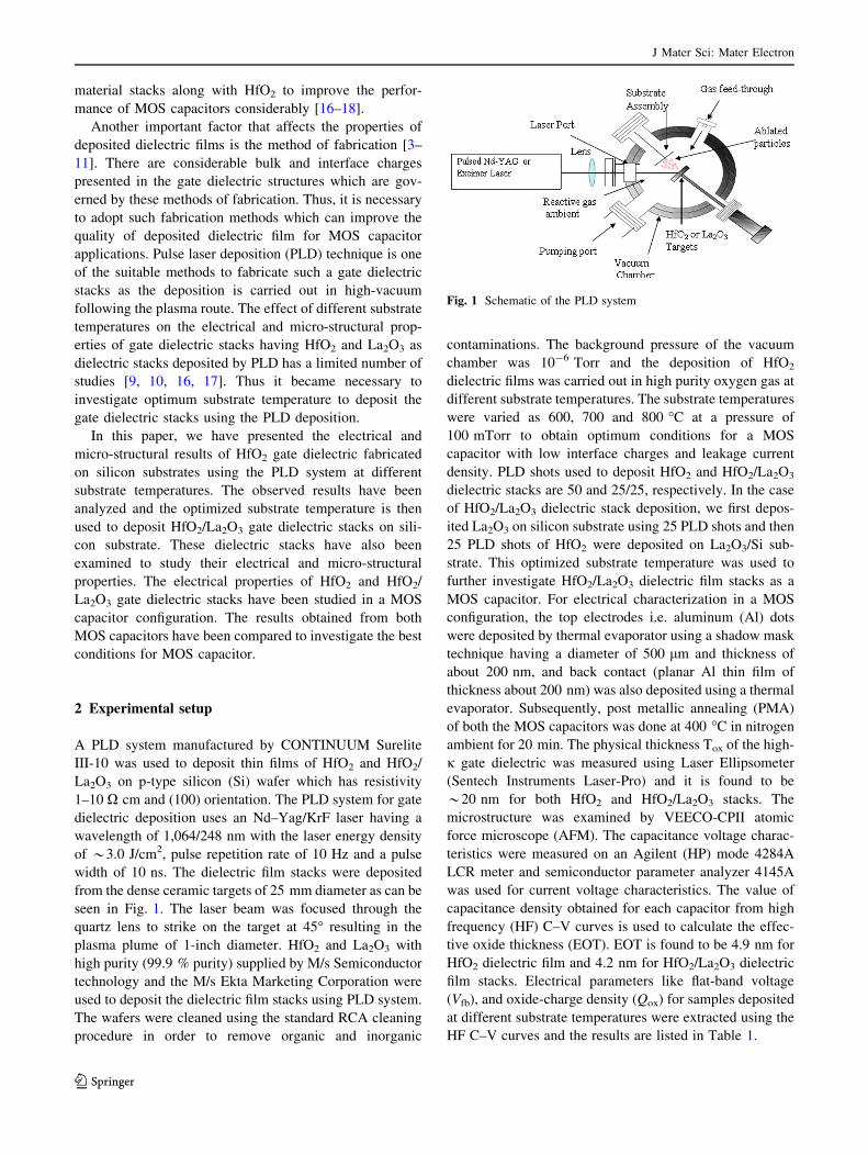
A PLD system manufactured by CONTINUUM Surelite
III-10 was used to deposit thin films of HfO2 and HfO2/
La2O3 on p-type silicon (Si) wafer which has resistivity
1–10 X cm and (100) orientation. The PLD system for gate
dielectric deposition uses an Nd–Yag/KrF laser having a
wavelength of 1,064/248 nm with the laser energy density
of *3.0 J/cm2, pulse repetition rate of 10 Hz and a pulse
width of 10 ns. The dielectric film stacks were deposited
from the dense ceramic targets of 25 mm diameter as can be
seen in Fig. 1. The laser beam was focused through the
quartz lens to strike on the target at 45� resulting in the
plasma plume of 1-inch diameter. HfO2 and La2O3 with
high purity (99.9 % purity) supplied by M/s Semiconductor
technology and the M/s Ekta Marketing Corporation were
used to deposit the dielectric film stacks using PLD system.
The wafers were cleaned using the standard RCA cleaning
procedure in order to remove organic and inorganic
contaminations. The background pressure of the vacuum
chamber was 10-6 Torr and the deposition of HfO2
dielectric films was carried out in high purity oxygen gas at
different substrate temperatures. The substrate temperatures
were varied as 600, 700 and 800 �C at a pressure of
100 mTorr to obtain optimum conditions for a MOS
capacitor with low interface charges and leakage current
density. PLD shots used to deposit HfO2 and HfO2/La2O3
dielectric stacks are 50 and 25/25, respectively. In the case
of HfO2/La2O3 dielectric stack deposition, we first depos-
ited La2O3 on silicon substrate using 25 PLD shots and then
25 PLD shots of HfO2 were deposited on La2O3/Si sub-
strate. This optimized substrate temperature was used to
further investigate HfO2/La2O3 dielectric film stacks as a
MOS capacitor. For electrical characterization in a MOS
configuration, the top electrodes i.e. aluminum (Al) dots
were deposited by thermal evaporator using a shadow mask
technique having a diameter of 500 lm and thickness of
about 200 nm, and back contact (planar Al thin film of
thickness about 200 nm) was also deposited using a thermal
evaporator. Subsequently, post metallic annealing (PMA)
of both the MOS capacitors was done at 400 �C in nitrogen
ambient for 20 min. The physical thickness Tox of the high-
j gate dielectric was measured using Laser Ellipsometer
(Sentech Instruments Laser-Pro) and it is found to be
*20 nm for both HfO2 and HfO2/La2O3 stacks. The
microstructure was examined by VEECO-CPII atomic
force microscope (AFM). The capacitance voltage charac-
teristics were measured on an Agilent (HP) mode 4284A
LCR meter and semiconductor parameter analyzer 4145A
was used for current voltage characteristics. The value of
capacitance density obtained for each capacitor from high
frequency (HF) C–V curves is used to calculate the effec-
tive oxide thickness (EOT). EOT is found to be 4.9 nm for
HfO2 dielectric film and 4.2 nm for HfO2/La2O3 dielectric
film stacks. Electrical parameters like flat-band voltage
(Vfb), and oxide-charge density (Qox) for samples deposited
at different substrate temperatures were extracted using the
HF C–V curves and the results are listed in Table 1.
Fig. 1 Schematic of the PLD system
J Mater Sci: Mater Electron
123
3 Results and discussion
Gate leakage current is an important device parameter. To
evaluate the gate leakage performance of MOS capacitors,
J–V characteristics are measured both in accumulation and
inversion region. The negative bias applied between the
metal gate and semiconductor is referred to as accumula-
tion region. In this region, the charge carriers (holes for
p-type MOS) appear at the oxide–semiconductor interface
and subsequently in strong accumulation region oxide
capacitance is measured. On the other hand, in an inversion
region on the application of positive voltage the minority
carriers (electrons) are attracted towards the gate and
accumulated at the interface of substrates and oxide film to
form an inversion layer. On application of certain positive
voltage, most of the minority carriers are in inversion
region, hence increasing the depletion layer to its maxi-
mum. At this stage, the measured capacitance has a mini-
mum value and often referred to as minimum capacitance.
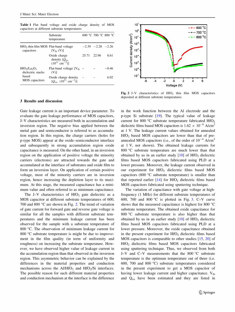
The J–V characteristics of HfO2 gate dielectric as a
MOS capacitor at different substrate temperatures of 600,
700 and 800 �C are shown in Fig. 2. The trend of variation
of gate current for forward gate and reverse gate voltage is
similar for all the samples with different substrate tem-
peratures and the minimum leakage current has been
observed for the sample with a substrate temperature of
800 �C. The observation of minimum leakage current for
800 �C substrate temperature is might be due to improve-
ment in the film quality (in term of uniformity and
roughness) on increasing the substrate temperature. How-
ever, we have observed higher value of leakage current in
the accumulation region than that observed in the inversion
region. This asymmetric behavior can be explained by the
differences in the material properties and conduction
mechanisms across the Al/HfO2 and HfO2/Si interfaces.
The possible reason for such different material properties
and conduction mechanism at the interface is the difference
in the work function between the Al electrode and the
p-type Si substrate [19]. The typical value of leakage
current for 800 �C substrate temperature fabricated HfO2
dielectric films based MOS capacitors is 1.62 9 10-6 A/cm2
at 1 V. The leakage current values obtained for annealed
HfO2 based MOS capacitors are lower than that of pre-
annealed MOS capacitors (i.e., of the order of 10-4 A/cm2
at 1 V, not shown). The obtained leakage currents for
800 �C substrate temperature are much lower than that
obtained by us in an earlier study [10] of HfO2 dielectric
films based MOS capacitors fabricated using PLD at a
lower pressure. Moreover, the leakage current observed in
our experiment for HfO2 dielectric films based MOS
capacitors (800 �C substrate temperature) is smaller than
that reported earlier [14] for HfO2 dielectric films based
MOS capacitors fabricated using sputtering technique.
The variation of capacitance with gate voltage at high-
frequency (1 MHz) for different substrate temperatures of
600, 700 and 800 �C is plotted in Fig. 3. C–V curve
shows that the measured capacitance is highest for 800 �C
substrate temperature. The obtained oxide capacitance for
800 �C substrate temperature is also higher than that
obtained by us in an earlier study [10] of HfO2 dielectric
films based MOS capacitors fabricated using PLD at a
lower pressure. Moreover, the oxide capacitance obtained
in the present experiment for HfO2 dielectric films based
MOS capacitors is comparable to other studies [15, 20] of
HfO2 dielectric films based MOS capacitors fabricated
using sputtering technique. Thus, we observed from both
J–V and C–V measurements that the 800 �C substrate
temperature is the optimum temperature out of three (i.e.
600, 700 and 800 �C) substrate temperatures considered
in the present experiment to get a MOS capacitor of
having lower leakage current and higher capacitance. Vfb
and Qox have been estimated and they are listed in
Fig. 2 J–V characteristics of HfO2 thin film MOS capacitors
deposited at different substrate temperatures
Table 1 Flat band voltage and oxide charge density of MOS
capacitors at different substrate temperatures
Substrate
temperature
600 �C 700 �C 800 �C
HfO2 thin film MOS
capacitors
Flat-band voltage
[Vfb (V)]
-2.39 -2.28 -2.26
Oxide charge
density [Qox
(1011 cm-2)]
25.71 22.96 8.61
HfO2/La2O3
dielectric stacks
based
MOS capacitors
Flat-band voltage [Vfb
(V)]
– – -0.46
Oxide charge density
[Qox (1011 cm-2)]
– – 6.02
J Mater Sci: Mater Electron
123
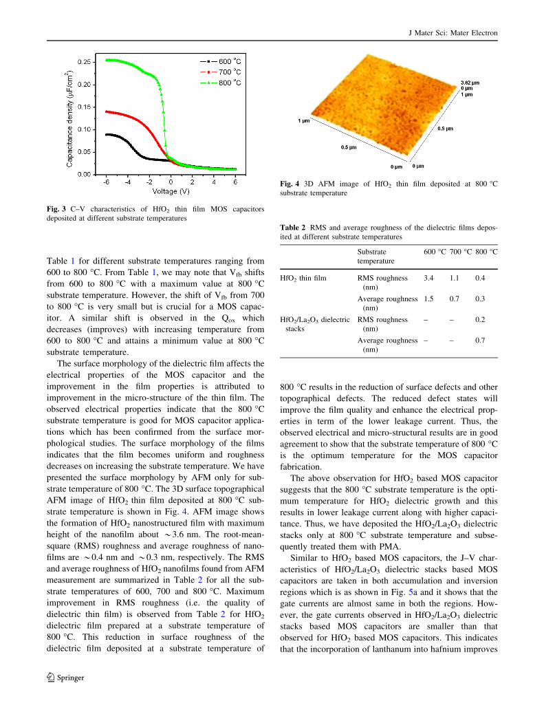
Table 1 for different substrate temperatures ranging from
600 to 800 �C. From Table 1, we may note that Vfb shifts
from 600 to 800 �C with a maximum value at 800 �C
substrate temperature. However, the shift of Vfb from 700
to 800 �C is very small but is crucial for a MOS capac-
itor. A similar shift is observed in the Qox which
decreases (improves) with increasing temperature from
600 to 800 �C and attains a minimum value at 800 �C
substrate temperature.
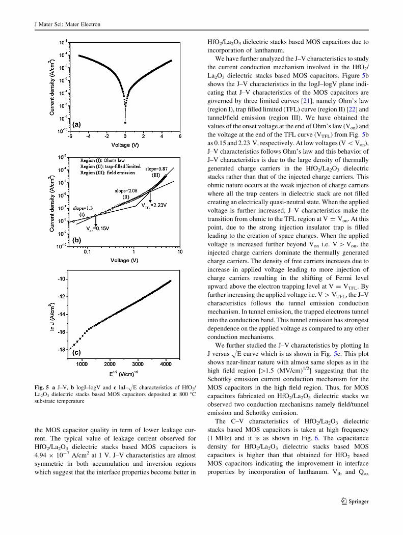
The surface morphology of the dielectric film affects the
electrical properties of the MOS capacitor and the
improvement in the film properties is attributed to
improvement in the micro-structure of the thin film. The
observed electrical properties indicate that the 800 �C
substrate temperature is good for MOS capacitor applica-
tions which has been confirmed from the surface mor-
phological studies. The surface morphology of the films
indicates that the film becomes uniform and roughness
decreases on increasing the substrate temperature. We have
presented the surface morphology by AFM only for sub-
strate temperature of 800 �C. The 3D surface topographical
AFM image of HfO2 thin film deposited at 800 �C sub-
strate temperature is shown in Fig. 4. AFM image shows
the formation of HfO2 nanostructured film with maximum
height of the nanofilm about *3.6 nm. The root-mean-
square (RMS) roughness and average roughness of nano-
films are *0.4 nm and *0.3 nm, respectively. The RMS
and average roughness of HfO2 nanofilms found from AFM
measurement are summarized in Table 2 for all the sub-
strate temperatures of 600, 700 and 800 �C. Maximum
improvement in RMS roughness (i.e. the quality of
dielectric thin film) is observed from Table 2 for HfO2
dielectric film prepared at a substrate temperature of
800 �C. This reduction in surface roughness of the
dielectric film deposited at a substrate temperature of
800 �C results in the reduction of surface defects and other
topographical defects. The reduced defect states will
improve the film quality and enhance the electrical prop-
erties in term of the lower leakage current. Thus, the
observed electrical and micro-structural results are in good
agreement to show that the substrate temperature of 800 �C
is the optimum temperature for the MOS capacitor
fabrication.
The above observation for HfO2 based MOS capacitor
suggests that the 800 �C substrate temperature is the opti-
mum temperature for HfO2 dielectric growth and this
results in lower leakage current along with higher capaci-
tance. Thus, we have deposited the HfO2/La2O3 dielectric
stacks only at 800 �C substrate temperature and subse-
quently treated them with PMA.
Similar to HfO2 based MOS capacitors, the J–V char-
acteristics of HfO2/La2O3 dielectric stacks based MOS
capacitors are taken in both accumulation and inversion
regions which is as shown in Fig. 5a and it shows that the
gate currents are almost same in both the regions. How-
ever, the gate currents observed in HfO2/La2O3 dielectric
stacks based MOS capacitors are smaller than that
observed for HfO2 based MOS capacitors. This indicates
that the incorporation of lanthanum into hafnium improves
Fig. 3 C–V characteristics of HfO2 thin film MOS capacitors
deposited at different substrate temperatures
Fig. 4 3D AFM image of HfO2 thin film deposited at 800 �C
substrate temperature
Table 2 RMS and average roughness of the dielectric films depos-
ited at different substrate temperatures
Substrate
temperature
600 �C 700 �C 800 �C
HfO2 thin film RMS roughness
(nm)
3.4 1.1 0.4
Average roughness
(nm)
1.5 0.7 0.3
HfO2/La2O3 dielectric
stacks
RMS roughness
(nm)
– – 0.2
Average roughness
(nm)
– – 0.7
J Mater Sci: Mater Electron
123
the MOS capacitor quality in term of lower leakage cur-
rent. The typical value of leakage current observed for
HfO2/La2O3 dielectric stacks based MOS capacitors is
4.94 9 10-7 A/cm2 at 1 V. J–V characteristics are almost
symmetric in both accumulation and inversion regions
which suggest that the interface properties become better in
HfO2/La2O3 dielectric stacks based MOS capacitors due to
incorporation of lanthanum.
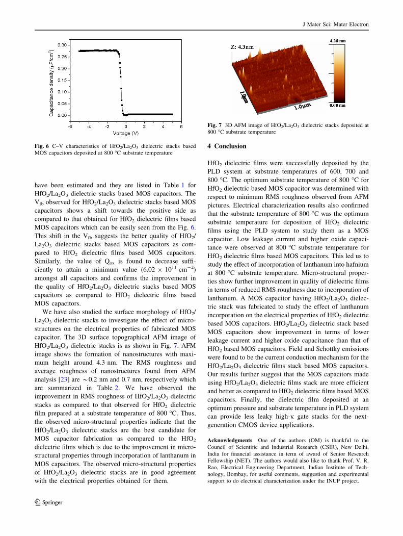
We have further analyzed the J–V characteristics to study
the current conduction mechanism involved in the HfO2/
La2O3 dielectric stacks based MOS capacitors. Figure 5b
shows the J–V characteristics in the logJ–logV plane indi-
cating that J–V characteristics of the MOS capacitors are
governed by three limited curves [21], namely Ohm’s law
(region I), trap filled limited (TFL) curve (region II) [22] and
tunnel/field emission (region III). We have obtained the
values of the onset voltage at the end of Ohm’s law (Von) and
the voltage at the end of the TFL curve (VTFL) from Fig. 5b
as 0.15 and 2.23 V, respectively. At low voltages (V \ Von),
J–V characteristics follows Ohm’s law and this behavior of
J–V characteristics is due to the large density of thermally
generated charge carriers in the HfO2/La2O3 dielectric
stacks rather than that of the injected charge carriers. This
ohmic nature occurs at the weak injection of charge carriers
where all the trap centers in dielectric stack are not filled
creating an electrically quasi-neutral state. When the applied
voltage is further increased, J–V characteristics make the
transition from ohmic to the TFL region at V = Von. At this
point, due to the strong injection insulator trap is filled
leading to the creation of space charges. When the applied
voltage is increased further beyond Von i.e. V [ Von, the
injected charge carriers dominate the thermally generated
charge carriers. The density of free carriers increases due to
increase in applied voltage leading to more injection of
charge carriers resulting in the shifting of Fermi level
upward above the electron trapping level at V = VTFL. By
further increasing the applied voltage i.e. V [ VTFL, the J–V
characteristics follows the tunnel emission conduction
mechanism. In tunnel emission, the trapped electrons tunnel
into the conduction band. This tunnel emission has strongest
dependence on the applied voltage as compared to any other
conduction mechanisms.
We further studied the J–V characteristics by plotting ln
J versus HE curve which is as shown in Fig. 5c. This plot
shows near-linear nature with almost same slopes as in the
high field region [[1.5 (MV/cm)1/2] suggesting that the
Schottky emission current conduction mechanism for the
MOS capacitors in the high field region. Thus, for MOS
capacitors fabricated on HfO2/La2O3 dielectric stacks we
observed two conduction mechanisms namely field/tunnel
emission and Schottky emission.
The C–V characteristics of HfO2/La2O3 dielectric
stacks based MOS capacitors is taken at high frequency
(1 MHz) and it is as shown in Fig. 6. The capacitance
density for HfO2/La2O3 dielectric stacks based MOS
capacitors is higher than that obtained for HfO2 based
MOS capacitors indicating the improvement in interface
properties by incorporation of lanthanum. Vfb and Qox
Fig. 5 a J–V, b logJ–logV and c lnJ–HE characteristics of HfO2/
La2O3 dielectric stacks based MOS capacitors deposited at 800 �C
substrate temperature
J Mater Sci: Mater Electron
123
have been estimated and they are listed in Table 1 for
HfO2/La2O3 dielectric stacks based MOS capacitors. The
Vfb observed for HfO2/La2O3 dielectric stacks based MOS
capacitors shows a shift towards the positive side as
compared to that obtained for HfO2 dielectric films based
MOS capacitors which can be easily seen from the Fig. 6.
This shift in the Vfb suggests the better quality of HfO2/
La2O3 dielectric stacks based MOS capacitors as com-
pared to HfO2 dielectric films based MOS capacitors.
Similarly, the value of Qox is found to decrease suffi-
ciently to attain a minimum value (6.02 9 1011 cm-2)
amongst all capacitors and confirms the improvement in
the quality of HfO2/La2O3 dielectric stacks based MOS
capacitors as compared to HfO2 dielectric films based
MOS capacitors.
We have also studied the surface morphology of HfO2/
La2O3 dielectric stacks to investigate the effect of micro-
structures on the electrical properties of fabricated MOS
capacitor. The 3D surface topographical AFM image of
HfO2/La2O3 dielectric stacks is as shown in Fig. 7. AFM
image shows the formation of nanostructures with maxi-
mum height around 4.3 nm. The RMS roughness and
average roughness of nanostructures found from AFM
analysis [23] are *0.2 nm and 0.7 nm, respectively which
are summarized in Table 2. We have observed the
improvement in RMS roughness of HfO2/La2O3 dielectric
stacks as compared to that observed for HfO2 dielectric
film prepared at a substrate temperature of 800 �C. Thus,
the observed micro-structural properties indicate that the
HfO2/La2O3 dielectric stacks are the best candidate for
MOS capacitor fabrication as compared to the HfO2
dielectric films which is due to the improvement in micro-
structural properties through incorporation of lanthanum in
MOS capacitors. The observed micro-structural properties
of HfO2/La2O3 dielectric stacks are in good agreement
with the electrical properties obtained for them.
4 Conclusion
HfO2 dielectric films were successfully deposited by the
PLD system at substrate temperatures of 600, 700 and
800 �C. The optimum substrate temperature of 800 �C for
HfO2 dielectric based MOS capacitor was determined with
respect to minimum RMS roughness observed from AFM
pictures. Electrical characterization results also confirmed
that the substrate temperature of 800 �C was the optimum
substrate temperature for deposition of HfO2 dielectric
films using the PLD system to study them as a MOS
capacitor. Low leakage current and higher oxide capaci-
tance were observed at 800 �C substrate temperature for
HfO2 dielectric films based MOS capacitors. This led us to
study the effect of incorporation of lanthanum into hafnium
at 800 �C substrate temperature. Micro-structural proper-
ties show further improvement in quality of dielectric films
in terms of reduced RMS roughness due to incorporation of
lanthanum. A MOS capacitor having HfO2/La2O3 dielec-
tric stack was fabricated to study the effect of lanthanum
incorporation on the electrical properties of HfO2 dielectric
based MOS capacitors. HfO2/La2O3 dielectric stack based
MOS capacitors show improvement in terms of lower
leakage current and higher oxide capacitance than that of
HfO2 based MOS capacitors. Field and Schottky emissions
were found to be the current conduction mechanism for the
HfO2/La2O3 dielectric films stack based MOS capacitors.
Our results further suggest that the MOS capacitors made
using HfO2/La2O3 dielectric films stack are more efficient
and better as compared to HfO2 dielectric films based MOS
capacitors. Finally, the dielectric film deposited at an
optimum pressure and substrate temperature in PLD system
can provide less leaky high-j gate stacks for the next-
generation CMOS device applications.
Acknowledgments One of the authors (OM) is thankful to the
Council of Scientific and Industrial Research (CSIR), New Delhi,
India for financial assistance in term of award of Senior Research
Fellowship (NET). The authors would also like to thank Prof. V. R.
Rao, Electrical Engineering Department, Indian Institute of Tech-
nology, Bombay, for useful comments, suggestion and experimental
support to do electrical characterization under the INUP project.
Fig. 6 C–V characteristics of HfO2/La2O3 dielectric stacks based
MOS capacitors deposited at 800 �C substrate temperature
Fig. 7 3D AFM image of HfO2/La2O3 dielectric stacks deposited at
800 �C substrate temperature
J Mater Sci: Mater Electron
123
References
1. H. Wong, H. Iwai, Microelectron. Eng. 83, 1867 (2006)
2. H. Wong, H. Iwai, Phys. World 18, 40 (2005)
3. T. Zimmermann, Y. Cao, D. Jena, H.G. Xing, Int. J. High Speed
Electron. Syst. 19, 153 (2009)
4. G.B. Alers, D.J. Werder, Y. Chabal, H.C. Lu, E.P. Gusev, E.
Garfunkel, T. Gustafsson, R.S. Urdahl, Appl. Phys. Lett. 73, 1517
(1998)
5. C.M. Tanner, Y.-C. Perng, C. Frewin, S.E. Saddow, J.P. Chang,
Appl. Phys. Lett. 91, 203510 (2007)
6. S. Chakraborty, M.K. Bera, S. Bhattacharya, C.K. Maiti, Mi-
croelectron. Eng. 81, 188 (2005)
7. D. Zade, S. Sato, K. Kakushima, A. Srivastava, P. Ahmet, K.
Tsutsui, A. Nishiyama, N. Sugii, K. Natori, T. Hattori, C.K.
Sarkar, H. Iwai, Microelectron. Reliab. 51, 746 (2011)
8. T. Ngai, W.J. Qi, R. Sharma, J. Fretwell, X. Chen, J.C. Lee, S.
Banerjee, Appl. Phys. Lett. 76, 502 (2000)
9. J. Zhu, Y.R. Li, Z.G. Liu, J. Phys. D Appl. Phys. 37, 2896 (2004)
10. A. Srivastava, R. K. Nahar, V. Gupta, C. K. Sarkar, Proceedings
of the 11th IEEE International Conference on Nanotechnology
(Portland, Oregon, USA, 2011), p. 504
11. R.K. Nahar, V. Singh, A. Sharma, J. Mater. Sci.: Mater. Electron.
18, 615 (2007)
12. A. Srivastava, R.K. Nahar, C.K. Sarkar, W.P. Singh, Y. Malhotra,
Microelectron. Reliab. 51, 751 (2011)
13. A. Srivastava, R.K. Nahar, C.K. Sarkar, J. Mater. Sci.: Mater.
Electron. 22, 882 (2011)
14. P.M. Tirmali, A.G. Khairnar, B.N. Joshi, A.M. Mahajan, Solid
State Electron. 62, 44 (2011)
15. K.L. Ng, N. Zhan, C.W. Kok, M.C. Poon, H. Wong, Micro-
electron. Reliab. 43, 1289 (2003)
16. J. Zhu, Z.G. Liu, Y.R. Li, J. Phys. D Appl. Phys. 38, 446 (2005)
17. J. Zhu, Z.G. Liu, Appl. Phys. A 80, 1769 (2005)
18. H.Y. Yu, J.F. Kang, C. Ren, J.D. Chen, Y.T. Hou, C. Shen, M.F.
Li, D.S.H. Chan, K.L. Bera, C.H. Tung, D.-L. Kwong, IEEE
Electron. Device Lett. 25, 70 (2004)
19. H.F. Wolf, Semiconductors (Wiley, New York, 1971)
20. H. Wong, K.L. Ng, N. Zhan, M.C. Poon, C.W. Kok, J. Vac. Sci.
Technol. B 22, 1094 (2004)
21. S.M. Sze, Physics of Semiconductor Devices, 2nd edn. (Wiley,
New York, 1981)
22. F.-C. Chiu, H.-W. Chou, J.Y.-M. Lee, J. Appl. Phys. 97, 103503
(2005)
23. I. Horcas, R. Fernandez, J.M. Gomez-Rodrıguez, J. Colchero, J.
Gomez-Herrero, A.M. Baro, Rev. Sci. Instrum. 78, 013705
(2007)
J Mater Sci: Mater Electron
123
Top Related