zWhere a is impurity gradient and W is depletion width area. 8.pdf · EEE132 Zulfiqar Ali 11...
27
EEE132 Zulfiqar Ali 1 Linearly Graded Junction The Poisson equation for the case is Where a is impurity gradient and W is depletion width area. ax q dx d s ε − = Ψ 2 2 2 2 W x W ≤ ≤ −
Transcript of zWhere a is impurity gradient and W is depletion width area. 8.pdf · EEE132 Zulfiqar Ali 11...
EEE132 Zulfiqar Ali 1
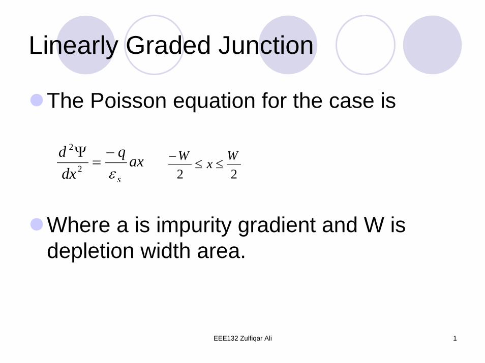
Linearly Graded Junction
The Poisson equation for the case is
Where a is impurity gradient and W is depletion width area.
axqdxd
sε−
=Ψ2
2
22WxW
≤≤−
EEE132 Zulfiqar Ali 2
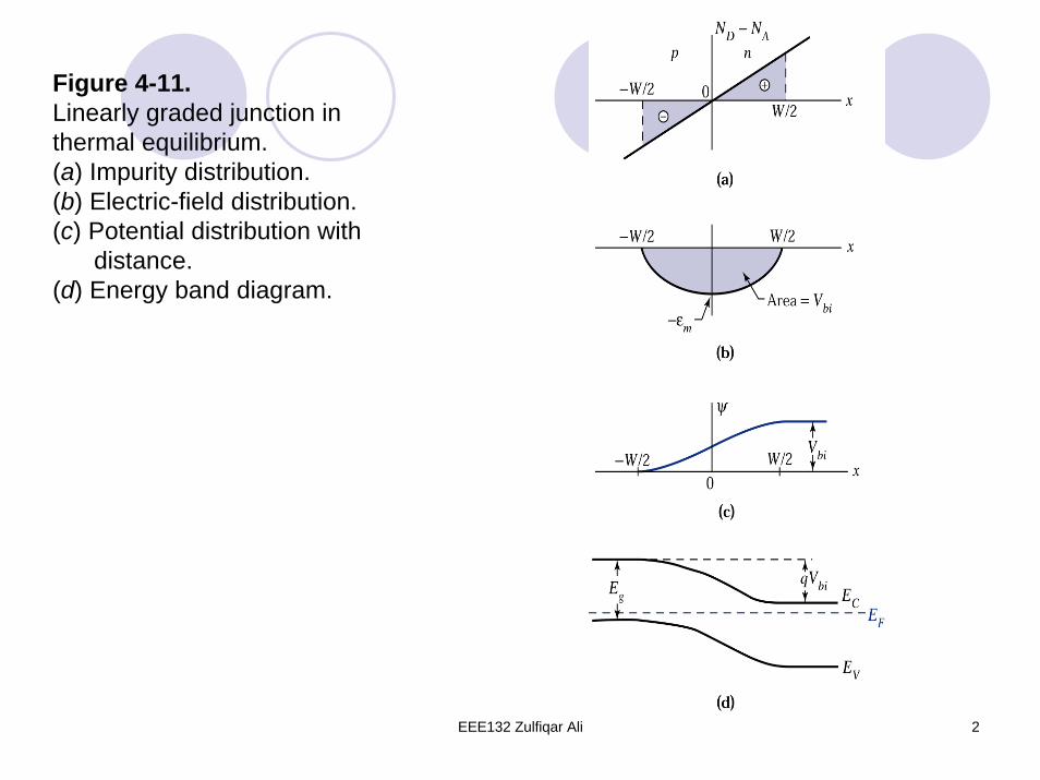
Figure 4-11.Linearly graded junction in thermal equilibrium. (a) Impurity distribution. (b) Electric-field distribution. (c) Potential distribution with
distance. (d) Energy band diagram.
EEE132 Zulfiqar Ali 3
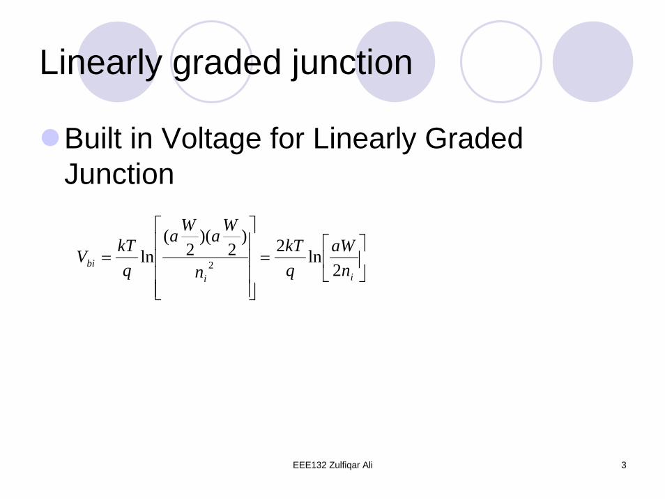
Linearly graded junction
Built in Voltage for Linearly Graded Junction
⎥⎦
⎤⎢⎣
⎡=
⎥⎥⎥⎥
⎦
⎤
⎢⎢⎢⎢
⎣
⎡
=ii
bi naW
qkT
n
WaWa
qkTV
2ln2)
2)(
2(
ln 2
EEE132 Zulfiqar Ali 4
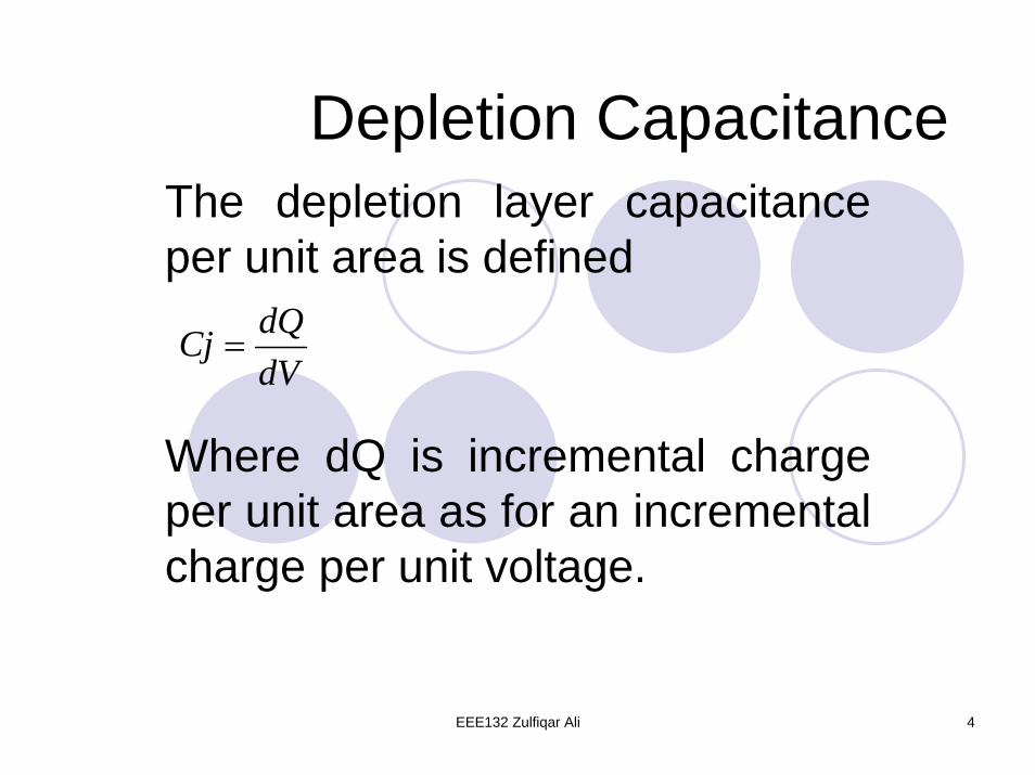
Depletion CapacitanceThe depletion layer capacitance per unit area is defined
Where dQ is incremental charge per unit area as for an incremental charge per unit voltage.
dVdQCj =
EEE132 Zulfiqar Ali 5
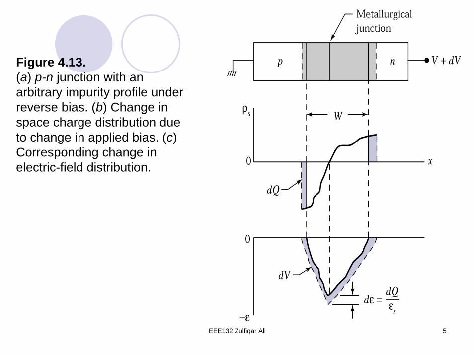
Figure 4.13.(a) p-n junction with an arbitrary impurity profile under reverse bias. (b) Change in space charge distribution due to change in applied bias. (c) Corresponding change in electric-field distribution.
EEE132 Zulfiqar Ali 6
Depletion Capacitance
Whenever voltage dv is applied. The charge filed distribution will expand. Figure shows the region bounded by dashed line.This increment bring increase in electric field by an amount of
s
dQdε
ε =
EEE132 Zulfiqar Ali 7
Capacitance-Voltage Characteristic
Separation between two plates represents the depletion width. Refer to the figure 13.For forward bias large current can flow across the junction corresponding to large number of mobile carrier.The incremental change of these mobile carriers with respect to the biasing voltage contributes an additional term called diffusion capacitance.
EEE132 Zulfiqar Ali 8
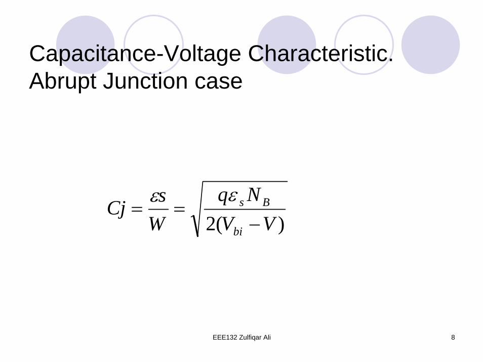
Capacitance-Voltage Characteristic.Abrupt Junction case
)(2 VVNq
WsCj
bi
Bs
−==
εε
EEE132 Zulfiqar Ali 9
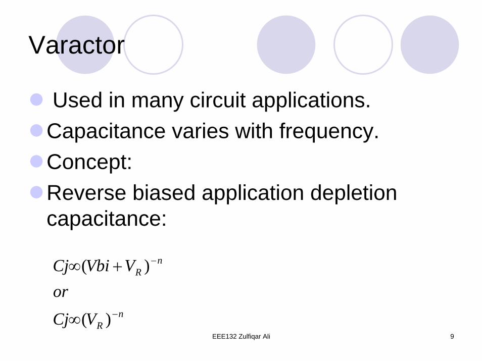
Varactor
Used in many circuit applications.Capacitance varies with frequency.Concept:Reverse biased application depletion capacitance:
nR
nR
VCjor
VVbiCj
−
−
∞
+∞
)(
)(
EEE132 Zulfiqar Ali 10
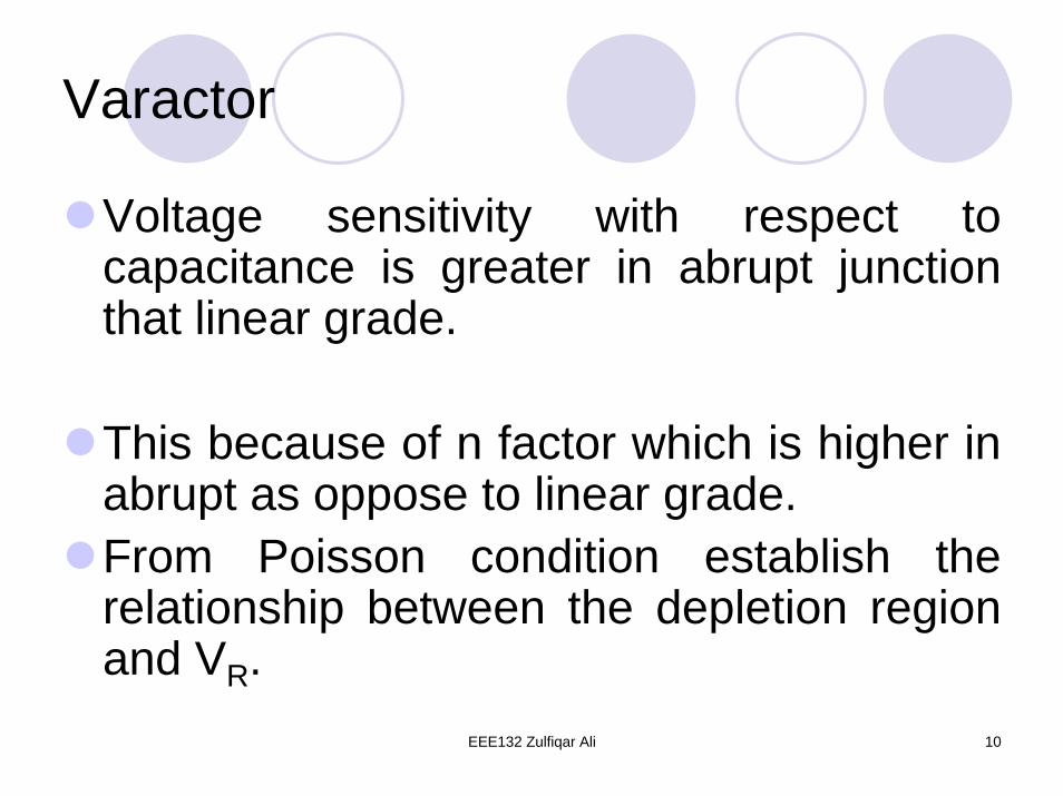
Varactor
Voltage sensitivity with respect to capacitance is greater in abrupt junction that linear grade.
This because of n factor which is higher in abrupt as oppose to linear grade.From Poisson condition establish the relationship between the depletion region and VR.
EEE132 Zulfiqar Ali 11
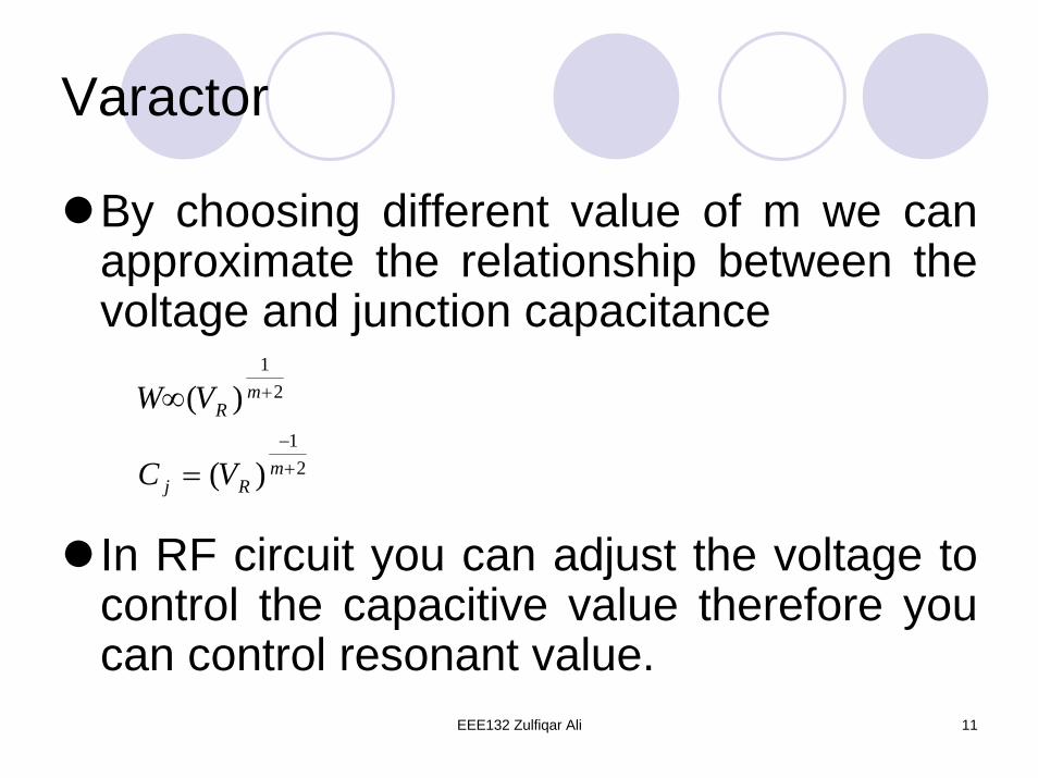
Varactor
By choosing different value of m we can approximate the relationship between the voltage and junction capacitance
In RF circuit you can adjust the voltage to control the capacitive value therefore you can control resonant value.
21
21
)(
)(
+−
+
=
∞
mRj
mR
VC
VW
EEE132 Zulfiqar Ali 12
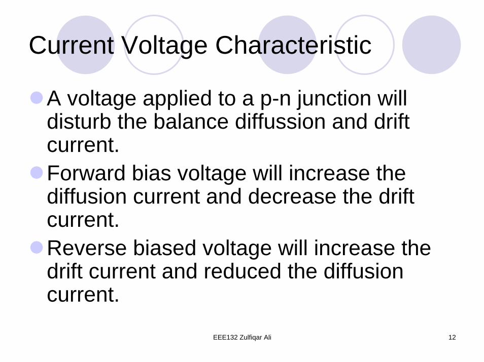
Current Voltage Characteristic
A voltage applied to a p-n junction will disturb the balance diffussion and drift current.Forward bias voltage will increase the diffusion current and decrease the drift current.Reverse biased voltage will increase the drift current and reduced the diffusion current.
EEE132 Zulfiqar Ali 13
Ideal characteristic.
We based on these assumptions:Abrupt boundaries ,outside the boundary the semiconductor assume to be neutral.Carrier density related by potential different.Low density carrier is smaller compare to higher density.Electron and hole are constant throughout the depletion region.
EEE132 Zulfiqar Ali 14
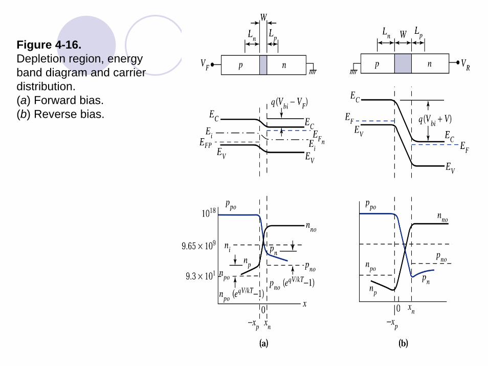
Figure 4-16.Depletion region, energy band diagram and carrier distribution. (a) Forward bias. (b) Reverse bias.
EEE132 Zulfiqar Ali 15
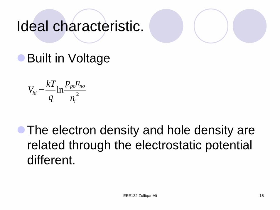
Ideal characteristic.
Built in Voltage
The electron density and hole density are related through the electrostatic potential different.
2lni
nopobi n
npqkTV =
EEE132 Zulfiqar Ali 16
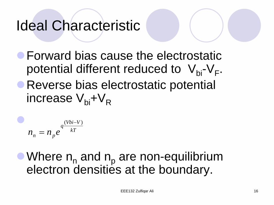
Ideal Characteristic
Forward bias cause the electrostatic potential different reduced to Vbi-VF.Reverse bias electrostatic potential increase Vbi+VR
Where nn and np are non-equilibrium electron densities at the boundary.
kTVVbiq
pn enn)( −
=
EEE132 Zulfiqar Ali 17
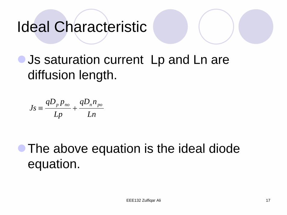
Ideal Characteristic
Js saturation current Lp and Ln are diffusion length.
The above equation is the ideal diode equation.
LnnqD
LppqD
Js ponnop +≡
EEE132 Zulfiqar Ali 18
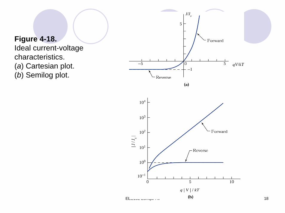
Figure 4-18.Ideal current-voltage characteristics. (a) Cartesian plot. (b) Semilog plot.
EEE132 Zulfiqar Ali 19
Temperature Effect
Temperature effect has an effect on the device performance.In reverse bias as well as forward bias the magnitude of diffusion and generation recombination depend strong on the temperature.
EEE132 Zulfiqar Ali 20
Charge storage and transient behavior
Under forward bias the electrons are injected into p-type and holes are injected into the n-type.Once injected across junction the minority carriers recombine with majority carrier and decay exponentially with distance.These lead to current flows and charge storage in the pn junction.
EEE132 Zulfiqar Ali 21
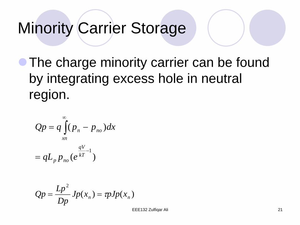
Minority Carrier Storage
The charge minority carrier can be found by integrating excess hole in neutral region.
)(
)(
1−
∞
=
−= ∫
kTqV
nop
xnnon
epqL
dxppqQp
)()(2
nn xpJpxJpDpLpQp τ==
EEE132 Zulfiqar Ali 22
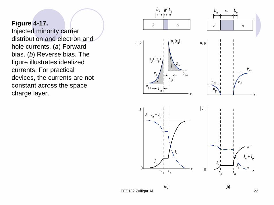
Figure 4-17.Injected minority carrier distribution and electron and hole currents. (a) Forward bias. (b) Reverse bias. The figure illustrates idealized currents. For practical devices, the currents are not constant across the space charge layer.
EEE132 Zulfiqar Ali 23
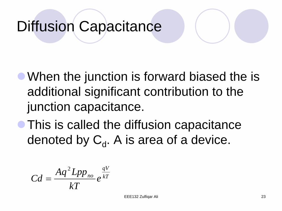
Diffusion Capacitance
When the junction is forward biased the is additional significant contribution to the junction capacitance.This is called the diffusion capacitance denoted by Cd. A is area of a device.
kTqV
no ekTLppAq
Cd2
=
EEE132 Zulfiqar Ali 24
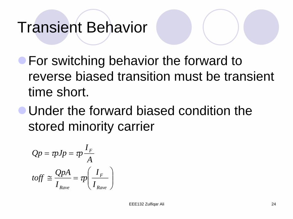
Transient Behavior
For switching behavior the forward to reverse biased transition must be transient time short.Under the forward biased condition the stored minority carrier
⎟⎟⎠
⎞⎜⎜⎝
⎛=≅
==
Rave
F
Rave
F
II
pIQpAtoff
AI
ppJpQp
τ
ττ
EEE132 Zulfiqar Ali 25
Junction Breakdown
When large reverse voltage is applied to p-n junction, the junction breaks down and conducts a very large current.The important breakdown mechanism:Tunneling process and avalancemechanism.
EEE132 Zulfiqar Ali 26
Tunneling Effect
High electric field is applied in reverse direction valence electron make transition from valence band to conduction band.Only occurs if the electric field is high about 106V/cm
EEE132 Zulfiqar Ali 27
Avalance multiplication
This occurs under the reverse bias condition.The thermally generated electron gain kinetic energy from the electric field.If the field is sufficiently high it can gain enough kinetic energy to break the bond creating electron hole pair.The newly created electron hole pair requires energy thus create more electron hole pair and this is called the avalance multiplication.