TS3A5223 0.45 Ω Dual SPDT Bidirectional Analog Switch … · • Deleted: "dt/dv, SEL pin Input...
22
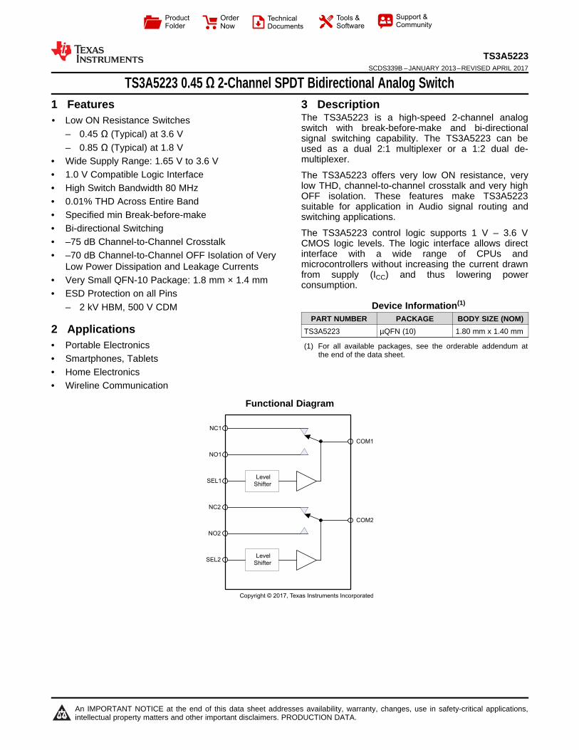
NC1 NC2 NO1 NO2 SEL1 SEL2 COM1 COM2 Level Shifter Level Shifter Copyright © 2017, Texas Instruments Incorporated Product Folder Order Now Technical Documents Tools & Software Support & Community An IMPORTANT NOTICE at the end of this data sheet addresses availability, warranty, changes, use in safety-critical applications, intellectual property matters and other important disclaimers. PRODUCTION DATA. TS3A5223 SCDS339B – JANUARY 2013 – REVISED APRIL 2017 TS3A5223 0.45 Ω 2-Channel SPDT Bidirectional Analog Switch 1 1 Features 1• Low ON Resistance Switches – 0.45 Ω (Typical) at 3.6 V – 0.85 Ω (Typical) at 1.8 V • Wide Supply Range: 1.65 V to 3.6 V • 1.0 V Compatible Logic Interface • High Switch Bandwidth 80 MHz • 0.01% THD Across Entire Band • Specified min Break-before-make • Bi-directional Switching • –75 dB Channel-to-Channel Crosstalk • –70 dB Channel-to-Channel OFF Isolation of Very Low Power Dissipation and Leakage Currents • Very Small QFN-10 Package: 1.8 mm × 1.4 mm • ESD Protection on all Pins – 2 kV HBM, 500 V CDM 2 Applications • Portable Electronics • Smartphones, Tablets • Home Electronics • Wireline Communication 3 Description The TS3A5223 is a high-speed 2-channel analog switch with break-before-make and bi-directional signal switching capability. The TS3A5223 can be used as a dual 2:1 multiplexer or a 1:2 dual de- multiplexer. The TS3A5223 offers very low ON resistance, very low THD, channel-to-channel crosstalk and very high OFF isolation. These features make TS3A5223 suitable for application in Audio signal routing and switching applications. The TS3A5223 control logic supports 1 V – 3.6 V CMOS logic levels. The logic interface allows direct interface with a wide range of CPUs and microcontrollers without increasing the current drawn from supply (I CC ) and thus lowering power consumption. Device Information (1) PART NUMBER PACKAGE BODY SIZE (NOM) TS3A5223 μQFN (10) 1.80 mm x 1.40 mm (1) For all available packages, see the orderable addendum at the end of the data sheet. Functional Diagram
Transcript of TS3A5223 0.45 Ω Dual SPDT Bidirectional Analog Switch … · • Deleted: "dt/dv, SEL pin Input...
NC1
NC2
NO1
NO2
SEL1
SEL2
COM1
COM2
Level
Shifter
Level
Shifter
Copyright © 2017, Texas Instruments Incorporated
Product
Folder
Order
Now
Technical
Documents
Tools &
Software
Support &Community
An IMPORTANT NOTICE at the end of this data sheet addresses availability, warranty, changes, use in safety-critical applications,intellectual property matters and other important disclaimers. PRODUCTION DATA.
TS3A5223SCDS339B –JANUARY 2013–REVISED APRIL 2017
TS3A5223 0.45 Ω 2-Channel SPDT Bidirectional Analog Switch
1
1 Features1• Low ON Resistance Switches
– 0.45 Ω (Typical) at 3.6 V– 0.85 Ω (Typical) at 1.8 V
• Wide Supply Range: 1.65 V to 3.6 V• 1.0 V Compatible Logic Interface• High Switch Bandwidth 80 MHz• 0.01% THD Across Entire Band• Specified min Break-before-make• Bi-directional Switching• –75 dB Channel-to-Channel Crosstalk• –70 dB Channel-to-Channel OFF Isolation of Very
Low Power Dissipation and Leakage Currents• Very Small QFN-10 Package: 1.8 mm × 1.4 mm• ESD Protection on all Pins
– 2 kV HBM, 500 V CDM
2 Applications• Portable Electronics• Smartphones, Tablets• Home Electronics• Wireline Communication
3 DescriptionThe TS3A5223 is a high-speed 2-channel analogswitch with break-before-make and bi-directionalsignal switching capability. The TS3A5223 can beused as a dual 2:1 multiplexer or a 1:2 dual de-multiplexer.
The TS3A5223 offers very low ON resistance, verylow THD, channel-to-channel crosstalk and very highOFF isolation. These features make TS3A5223suitable for application in Audio signal routing andswitching applications.
The TS3A5223 control logic supports 1 V – 3.6 VCMOS logic levels. The logic interface allows directinterface with a wide range of CPUs andmicrocontrollers without increasing the current drawnfrom supply (ICC) and thus lowering powerconsumption.
Device Information(1)
PART NUMBER PACKAGE BODY SIZE (NOM)TS3A5223 µQFN (10) 1.80 mm x 1.40 mm
(1) For all available packages, see the orderable addendum atthe end of the data sheet.
Functional Diagram
2
TS3A5223SCDS339B –JANUARY 2013–REVISED APRIL 2017 www.ti.com
Product Folder Links: TS3A5223
Submit Documentation Feedback Copyright © 2013–2017, Texas Instruments Incorporated
Table of Contents1 Features .................................................................. 12 Applications ........................................................... 13 Description ............................................................. 14 Revision History..................................................... 25 Pin Configuration and Functions ......................... 36 Specifications......................................................... 4
6.1 Absolute Maximum Ratings ...................................... 46.2 ESD Ratings ............................................................ 46.3 Recommended Operating Conditions....................... 46.4 Thermal Information .................................................. 46.5 Electrical Characteristics........................................... 56.6 Typical Characteristics .............................................. 6
7 Parameter Measurement Information .................. 78 Detailed Description ............................................ 10
8.1 Overview ................................................................. 108.2 Functional Block Diagram ....................................... 108.3 Feature Description................................................. 10
8.4 Device Functional Modes........................................ 119 Application and Implementation ........................ 12
9.1 Application Information............................................ 129.2 Typical Application ................................................. 12
10 Power Supply Recommendations ..................... 1311 Layout................................................................... 14
11.1 Layout Guidelines ................................................. 1411.2 Layout Example .................................................... 14
12 Device and Documentation Support ................. 1512.1 Documentation Support ....................................... 1512.2 Receiving Notification of Documentation Updates 1512.3 Community Resources.......................................... 1512.4 Trademarks ........................................................... 1512.5 Electrostatic Discharge Caution............................ 1512.6 Glossary ................................................................ 15
13 Mechanical, Packaging, and OrderableInformation ........................................................... 15
4 Revision HistoryNOTE: Page numbers for previous revisions may differ from page numbers in the current version.
Changes from Revision A (February 2013) to Revision B Page
• Added the Device Information table, ESD Ratings table, Thermal Information table, Feature Description section,Device Functional Modes, Application and Implementation section, Power Supply Recommendations section,Layout section, Device and Documentation Support section, and Mechanical, Packaging, and Orderable Informationsection .................................................................................................................................................................................... 1
• Changed the VMax MAX value From: 3.6 V To: VCC in the Recommended Operating Conditions table ................................ 4• Deleted: "dt/dv, SEL pin Input rise and fall time limit" from the Recommended Operating Conditions table......................... 4• Deleted the Dissipation Ratings table..................................................................................................................................... 4
Changes from Original (January 2013) to Revision A Page
• Changed the device status From: Preview To: Production ................................................................................................... 1
TS3A5223
NO2
VC
C
8
9
10
2N
O1
1
SEL2
COM2
67
COM1
GN
D
5
4
3
NC1
SEL1
NC
2
3
TS3A5223www.ti.com SCDS339B –JANUARY 2013–REVISED APRIL 2017
Product Folder Links: TS3A5223
Submit Documentation FeedbackCopyright © 2013–2017, Texas Instruments Incorporated
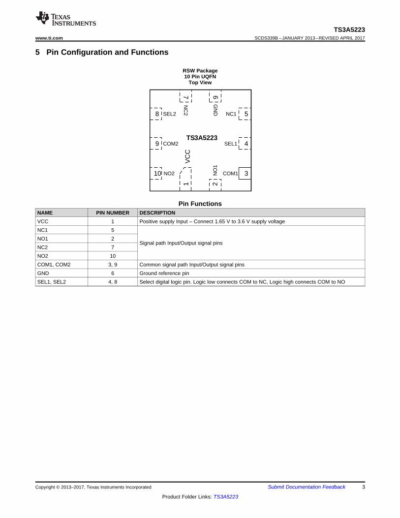
5 Pin Configuration and Functions
RSW Package10 Pin UQFN
Top View
Pin FunctionsNAME PIN NUMBER DESCRIPTIONVCC 1 Positive supply Input – Connect 1.65 V to 3.6 V supply voltageNC1 5
Signal path Input/Output signal pinsNO1 2NC2 7NO2 10COM1, COM2 3, 9 Common signal path Input/Output signal pinsGND 6 Ground reference pinSEL1, SEL2 4, 8 Select digital logic pin. Logic low connects COM to NC, Logic high connects COM to NO
4
TS3A5223SCDS339B –JANUARY 2013–REVISED APRIL 2017 www.ti.com
Product Folder Links: TS3A5223
Submit Documentation Feedback Copyright © 2013–2017, Texas Instruments Incorporated
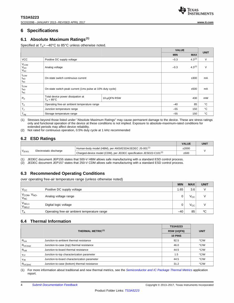
(1) Stresses beyond those listed under "Absolute Maximum Ratings" may cause permanent damage to the device. These are stress ratingsonly and functional operation of the device at these conditions is not implied. Exposure to absolute-maximum-rated conditions forextended periods may affect device reliability.
(2) Not rated for continuous operation, 0.5% duty cycle at 1 kHz recommended
6 Specifications
6.1 Absolute Maximum Ratings (1)
Specified at TA= –40°C to 85°C unless otherwise noted.VALUE
UNITMIN MAX
VCC Positive DC supply voltage –0.3 4.3 (2) V
VCOMVNOVNC
Analog voltage –0.3 4.3 (2) V
ICOMINOINC
On-state switch continuous current ±300 mA
ICOMINOINC
On-state switch peak current (1ms pulse at 10% duty cycle) ±500 mA
PDTotal device power dissipation atTA = 85°C 10-µQFN RSW 430 mW
TA Operating free-air ambient temperature range –40 85 °C
TJ Junction temperature range –55 150 °C
Tstg Storage temperature range –55 150 °C
(1) JEDEC document JEP155 states that 500-V HBM allows safe manufacturing with a standard ESD control process.(2) JEDEC document JEP157 states that 250-V CDM allows safe manufacturing with a standard ESD control process.
6.2 ESD RatingsVALUE UNIT
V(ESD) Electrostatic dischargeHuman-body model (HBM), per ANSI/ESDA/JEDEC JS-001 (1) ±2000
VCharged-device model (CDM), per JEDEC specification JESD22-C101 (2) ±500
6.3 Recommended Operating Conditionsover operating free-air temperature range (unless otherwise noted)
MIN MAX UNITVCC Positive DC supply voltage 1.65 3.6 VVCOM, VNO,VNC
Analog voltage range 0 VCC V
VSEL1VSEL2
Digital logic voltage 0 VCC V
TA Operating free-air ambient temperature range –40 85 ºC
(1) For more information about traditional and new thermal metrics, see the Semiconductor and IC Package Thermal Metrics applicationreport.
6.4 Thermal Information
THERMAL METRIC (1)
TS3A5223
UNITRSW (UQFN)
10 PINS
RθJA Junction-to-ambient thermal resistance 92.5 °C/W
RθJC(top) Junction-to-case (top) thermal resistance 46.0 °C/W
RθJB Junction-to-board thermal resistance 44.5 °C/W
ψJT Junction-to-top characterization parameter 1.5 °C/W
ψJB Junction-to-board characterization parameter 44.5 °C/W
RθJC(bot) Junction-to-case (bottom) thermal resistance 31.2 °C/W
5
TS3A5223www.ti.com SCDS339B –JANUARY 2013–REVISED APRIL 2017
Product Folder Links: TS3A5223
Submit Documentation FeedbackCopyright © 2013–2017, Texas Instruments Incorporated
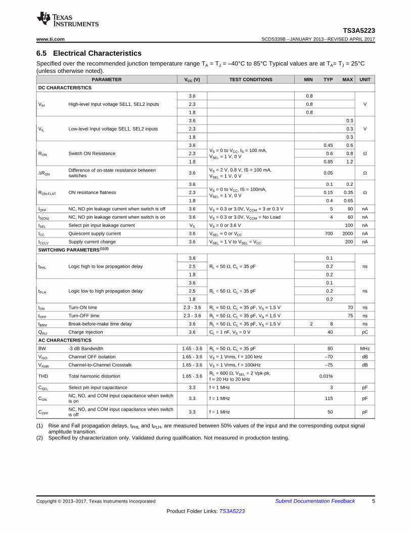
(1) Rise and Fall propagation delays, tPHL and tPLH, are measured between 50% values of the input and the corresponding output signalamplitude transition.
(2) Specified by characterization only. Validated during qualification. Not measured in production testing.
6.5 Electrical CharacteristicsSpecified over the recommended junction temperature range TA = TJ = –40°C to 85°C Typical values are at TA= TJ = 25°C(unless otherwise noted).
PARAMETER VCC (V) TEST CONDITIONS MIN TYP MAX UNIT
DC CHARACTERISTICS
VIH High-level Input voltage SEL1, SEL2 inputs
3.6 0.8
V2.3 0.8
1.8 0.8
VIL Low-level Input voltage SEL1, SEL2 inputs
3.6 0.3
V2.3 0.3
1.8 0.3
RON Switch ON Resistance
3.6VS = 0 to VCC, IS = 100 mA,VSEL = 1 V, 0 V
0.45 0.6
Ω2.3 0.6 0.8
1.8 0.85 1.2
ΔRONDifference of on-state resistance betweenswitches 3.6 VS = 2 V, 0.8 V, IS = 100 mA,
VSEL = 1 V, 0 V 0.05 Ω
RON-FLAT ON resistance flatness
3.6VS = 0 to VCC, IS = 100mA,VSEL = 1 V, 0 V
0.1 0.2
Ω2.3 0.15 0.35
1.8 0.4 0.65
IOFF NC, NO pin leakage current when switch is off 3.6 VS = 0.3 or 3.0V, VCOM = 3 or 0.3 V 5 90 nA
IS(ON) NC, NO pin leakage current when switch is on 3.6 VS = 0.3 or 3.0V, VCOM = No Load 4 60 nA
ISEL Select pin input leakage current VS VS = 0 or 3.6 V 100 nA
ICC Quiescent supply current 3.6 VSEL = 0 or VCC 700 2000 nA
ICCLV Supply current change 3.6 VSEL = 1 V to VSEL = VCC 200 nA
SWITCHING PARAMETERS (1) (2)
tPHL Logic high to low propagation delay
3.6
RL = 50 Ω, CL = 35 pF
0.1
ns2.5 0.2
1.8 0.2
tPLH Logic low to high propagation delay
3.6
RL = 50 Ω, CL = 35 pF
0.1
ns2.5 0.2
1.8 0.2
tON Turn-ON time 2.3 - 3.6 RL = 50 Ω, CL = 35 pF, VS = 1.5 V 70 ns
tOFF Turn-OFF time 2.3 - 3.6 RL = 50 Ω, CL = 35 pF, VS = 1.5 V 75 ns
tBBM Break-before-make time delay 3.6 RL = 50 Ω, CL = 35 pF, VS = 1.5 V 2 8 ns
QINJ Charge Injection 3.6 CL = 1 nF, VS = 0 V 40 pC
AC CHARACTERISTICS
BW -3 dB Bandwidth 1.65 - 3.6 RL = 50 Ω, CL = 35 pF 80 MHz
VISO Channel OFF isolation 1.65 - 3.6 VS = 1 Vrms, f = 100 kHz –70 dB
VXtalk Channel-to-Channel Crosstalk 1.65 - 3.6 VS = 1 Vrms, f = 100kHz –75 dB
THD Total harmonic distortion 1.65 - 3.6 RL = 600 Ω, VSEL = 2 Vpk-pk,f = 20 Hz to 20 kHz 0.01%
CSEL Select pin input capacitance 3.3 f = 1 MHz 3 pF
CONNC, NO, and COM input capacitance when switchis on 3.3 f = 1 MHz 115 pF
COFFNC, NO, and COM input capacitance when switchis off 3.3 f = 1 MHz 50 pF
0
0.1
0.2
0.3
0.4
0.5
0.6
0.7
0.8
0.9
0 0.5 1 1.5 2 2.5 3 3.5 4
Rds
on(
)
Vin(V)
1.8V
2.3V
3.0V
3.6V
C003 C003
0
0.002
0.004
0.006
0.008
0.01
0.012
0.014
10 100 1k 10k 100k
TH
D(%
)
Freq(Hz)
1.8V
2.3V
3.6V
C003 C003
0
0.1
0.2
0.3
0.4
0.5
0.6
0 0.5 1 1.5 2 2.5 3 3.5
Rds
on(
)
Vin(V)
-40C
25C
85C
C003 C003
0
0.1
0.2
0.3
0.4
0.5
0.6
0 0.5 1 1.5 2 2.5 3 3.5 4
Rds
on(
)
Vin(V)
-40C
25C
85C
C003 C003
0
0.1
0.2
0.3
0.4
0.5
0.6
0.7
0.8
0.9
0 0.5 1 1.5 2
Rds
on(
)
Vin(V)
-40C
25C
85C
C003 C003
0
0.1
0.2
0.3
0.4
0.5
0.6
0.7
0 0.5 1 1.5 2 2.5
Rds
on(
)
Vin(V)
-40C
25C
85C
C003 C003
6
TS3A5223SCDS339B –JANUARY 2013–REVISED APRIL 2017 www.ti.com
Product Folder Links: TS3A5223
Submit Documentation Feedback Copyright © 2013–2017, Texas Instruments Incorporated
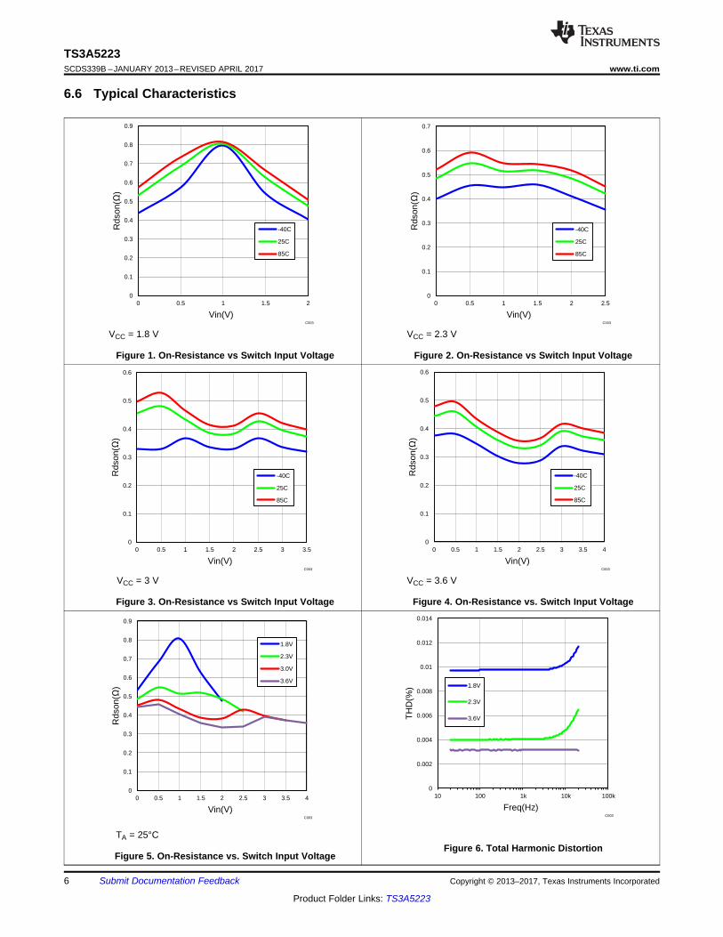
6.6 Typical Characteristics
VCC = 1.8 V
Figure 1. On-Resistance vs Switch Input Voltage
VCC = 2.3 V
Figure 2. On-Resistance vs Switch Input Voltage
VCC = 3 V
Figure 3. On-Resistance vs Switch Input Voltage
VCC = 3.6 V
Figure 4. On-Resistance vs. Switch Input Voltage
TA = 25°C
Figure 5. On-Resistance vs. Switch Input VoltageFigure 6. Total Harmonic Distortion
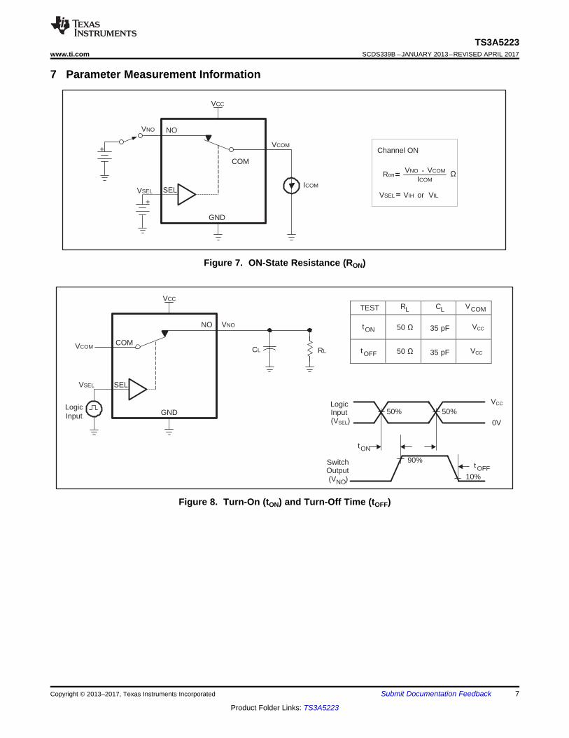
TEST RL CL VCOM
tON
50
35 pF
VCC
t OFF
50
35 pF
VCC
SEL
Logic Input (VSEL)
Switch Output (VNO)
tON
t OFF 90%
10%
VNONO
VSEL
VCOMCOM
GND
CL RL
Logic Input
VCC
VCC
50%50%
0V
+
SEL
+
VNO NO
VSEL
VCOM
ICOM
COM
GND
RonVCOMVNO
ICOM
Channel ON
-
VSEL VIH or VIL
VCC
7
TS3A5223www.ti.com SCDS339B –JANUARY 2013–REVISED APRIL 2017
Product Folder Links: TS3A5223
Submit Documentation FeedbackCopyright © 2013–2017, Texas Instruments Incorporated
7 Parameter Measurement Information
Figure 7. ON-State Resistance (RON)
Figure 8. Turn-On (tON) and Turn-Off Time (tOFF)
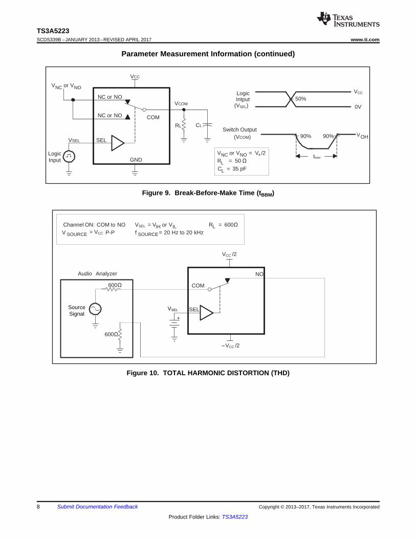
Channel ON: COM to NO VSEL = VIH or VIL RL = 600 V SOURCE = VCC P-P f SOURCE = 20 Hz to 20 kHz
VCC /2
Audio Analyzer
600
NO COM
SEL
+
600
±VCC /2
VSELSourceSignal
VNC or VNO NC or NO
NC or NO
VOH
VNC or VNO = V+/2 RL = 50
CL = 35 pF
SELVSEL
VCOM
COM
GND
VCC
Logic Intput
(VSEL)
VCC
50%
0V
90% 90%
CLRL
Logic Input
Switch Output(VCOM)
tBBM
8
TS3A5223SCDS339B –JANUARY 2013–REVISED APRIL 2017 www.ti.com
Product Folder Links: TS3A5223
Submit Documentation Feedback Copyright © 2013–2017, Texas Instruments Incorporated
Parameter Measurement Information (continued)
Figure 9. Break-Before-Make Time (tBBM)
Figure 10. TOTAL HARMONIC DISTORTION (THD)
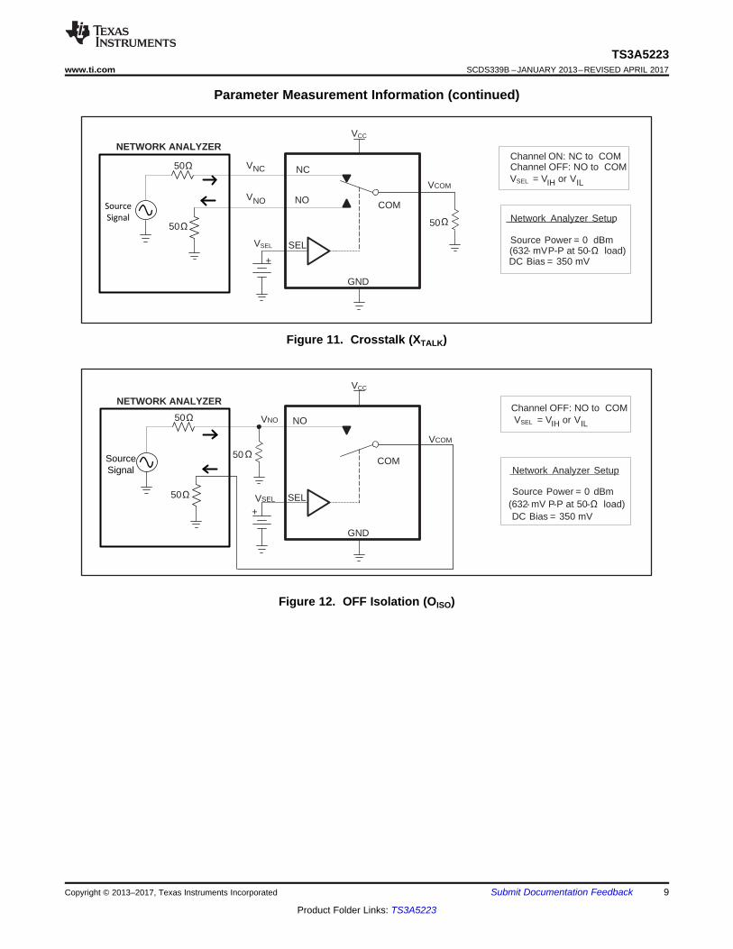
Channel OFF: NO to COM VSEL = VIH or VIL
Network Analyzer Setup
Source Power = 0 dBm (632- mV P-P at 50- load)
+ DC Bias = 350 mV
SEL
VNO NO
VSEL
VCOM
COM
GND
VCC
50
50
Source Signal
NETWORK ANALYZER
50
VNC NC
VNO NO
SEL
+
Channel ON: NC to COM Channel OFF: NO to COM VSEL = VIH or VIL
Network Analyzer Setup
Source Power = 0 dBm (632- mV P-P at 50- load) DC Bias = 350 mV
VSEL
COM
VCOM
Source
Signal
NETWORK ANALYZER
50
GND
VCC
50
50
9
TS3A5223www.ti.com SCDS339B –JANUARY 2013–REVISED APRIL 2017
Product Folder Links: TS3A5223
Submit Documentation FeedbackCopyright © 2013–2017, Texas Instruments Incorporated
Parameter Measurement Information (continued)
Figure 11. Crosstalk (XTALK)
Figure 12. OFF Isolation (OISO)
NC1
NC2
NO1
NO2
SEL1
SEL2
COM1
COM2
Level
Shifter
Level
Shifter
Copyright © 2017, Texas Instruments Incorporated
10
TS3A5223SCDS339B –JANUARY 2013–REVISED APRIL 2017 www.ti.com
Product Folder Links: TS3A5223
Submit Documentation Feedback Copyright © 2013–2017, Texas Instruments Incorporated
8 Detailed Description
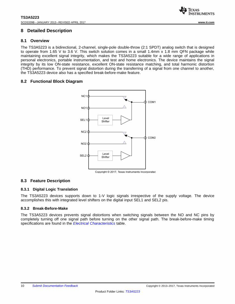
8.1 OverviewThe TS3A5223 is a bidirectional, 2-channel, single-pole double-throw (2:1 SPDT) analog switch that is designedto operate from 1.65 V to 3.6 V. This switch solution comes in a small 1.4mm x 1.8 mm QFN package whilemaintaining excellent signal integrity, which makes the TS3A5223 suitable for a wide range of applications inpersonal electronics, portable instrumentation, and test and home electronics. The device maintains the signalintegrity by its low ON-state resistance, excellent ON-state resistance matching, and total harmonic distortion(THD) performance. To prevent signal distortion during the transferring of a signal from one channel to another,the TS3A5223 device also has a specified break-before-make feature.
8.2 Functional Block Diagram
8.3 Feature Description
8.3.1 Digital Logic TranslationThe TS3A5223 devices supports down to 1-V logic signals irrespective of the supply voltage. The deviceaccomplishes this with integrated level shifters on the digital input SEL1 and SEL2 pis.
8.3.2 Break-Before-MakeThe TS3A5223 devices prevents signal distortions when switching signals between the NO and NC pins bycompletely turning off one signal path before turning on the other signal path. The break-before-make timingspecifications are found in the Electrical Characteristics table.
11
TS3A5223www.ti.com SCDS339B –JANUARY 2013–REVISED APRIL 2017
Product Folder Links: TS3A5223
Submit Documentation FeedbackCopyright © 2013–2017, Texas Instruments Incorporated
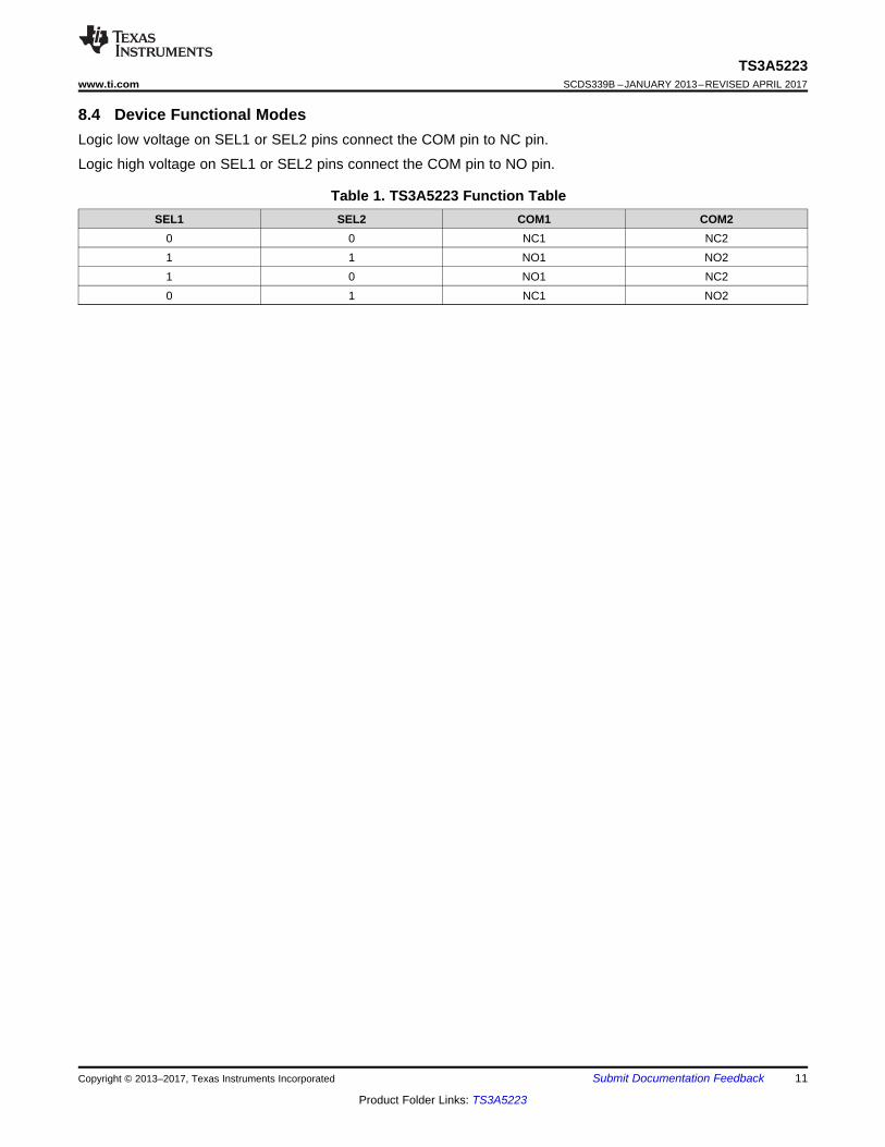
8.4 Device Functional ModesLogic low voltage on SEL1 or SEL2 pins connect the COM pin to NC pin.
Logic high voltage on SEL1 or SEL2 pins connect the COM pin to NO pin.
Table 1. TS3A5223 Function TableSEL1 SEL2 COM1 COM2
0 0 NC1 NC21 1 NO1 NO21 0 NO1 NC20 1 NC1 NO2
TS3A5223VCC
SEL1SEL2
COM1
COM4
GND
NO1
SystemController
Device 1
Device 2
0.1 PF0.1 PF
3.3 V
Signal Path
Switch Control Logic NC1
Device 3NO2
NC2 Device 4COM2
Copyright © 2017, Texas Instruments Incorporated
12
TS3A5223SCDS339B –JANUARY 2013–REVISED APRIL 2017 www.ti.com
Product Folder Links: TS3A5223
Submit Documentation Feedback Copyright © 2013–2017, Texas Instruments Incorporated
9 Application and Implementation
NOTEInformation in the following applications sections is not part of the TI componentspecification, and TI does not warrant its accuracy or completeness. TI’s customers areresponsible for determining suitability of components for their purposes. Customers shouldvalidate and test their design implementation to confirm system functionality.
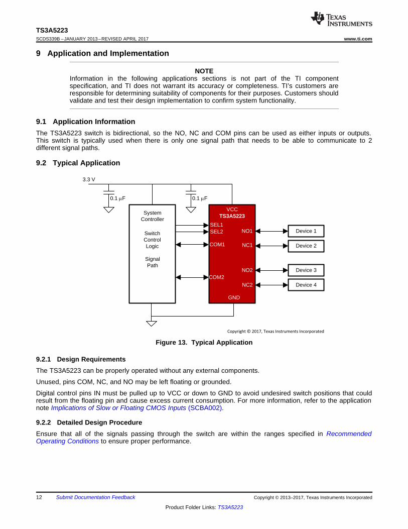
9.1 Application InformationThe TS3A5223 switch is bidirectional, so the NO, NC and COM pins can be used as either inputs or outputs.This switch is typically used when there is only one signal path that needs to be able to communicate to 2different signal paths.
9.2 Typical Application
Figure 13. Typical Application
9.2.1 Design RequirementsThe TS3A5223 can be properly operated without any external components.
Unused, pins COM, NC, and NO may be left floating or grounded.
Digital control pins IN must be pulled up to VCC or down to GND to avoid undesired switch positions that couldresult from the floating pin and cause excess current consumption. For more information, refer to the applicationnote Implications of Slow or Floating CMOS Inputs (SCBA002).
9.2.2 Detailed Design ProcedureEnsure that all of the signals passing through the switch are within the ranges specified in RecommendedOperating Conditions to ensure proper performance.
0
0.1
0.2
0.3
0.4
0.5
0.6
0 0.5 1 1.5 2 2.5 3 3.5 4
Rds
on(
)
Vin(V)
-40C
25C
85C
C003 C003
13
TS3A5223www.ti.com SCDS339B –JANUARY 2013–REVISED APRIL 2017
Product Folder Links: TS3A5223
Submit Documentation FeedbackCopyright © 2013–2017, Texas Instruments Incorporated
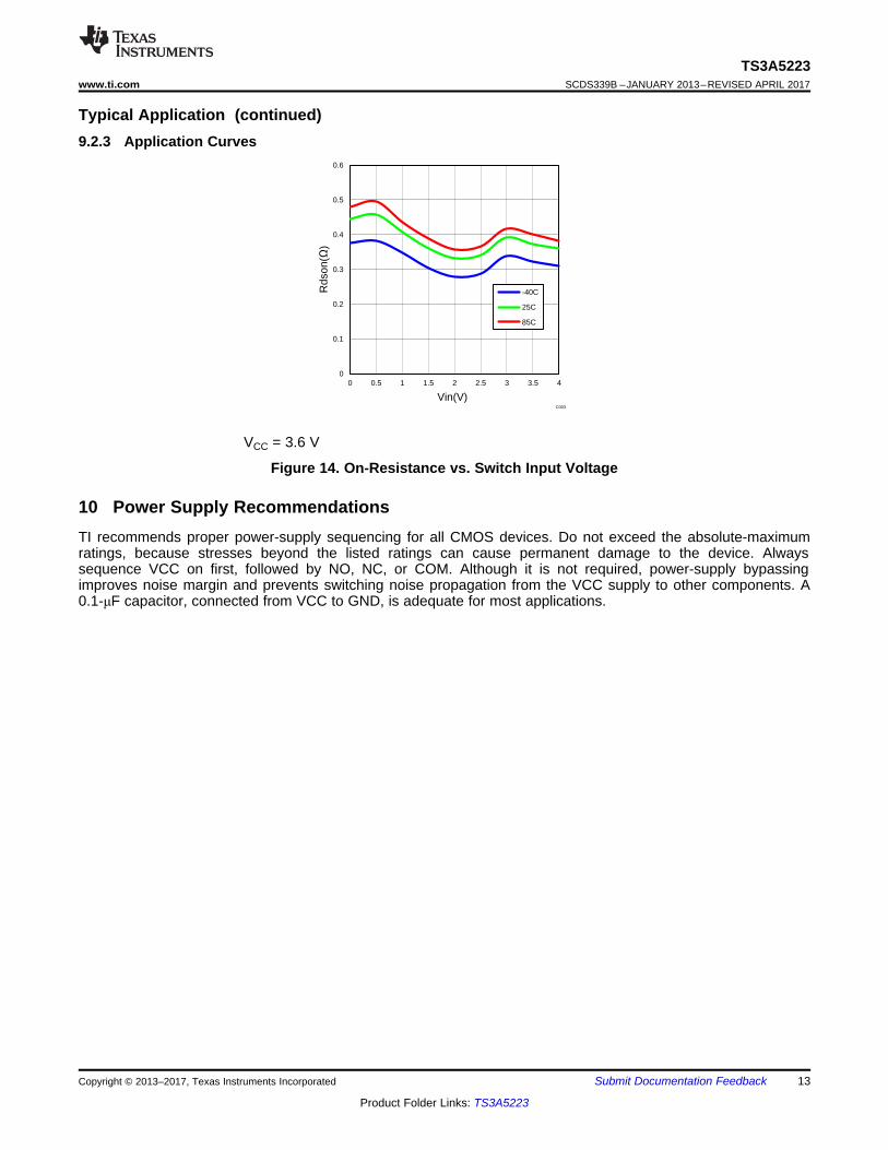
Typical Application (continued)9.2.3 Application Curves
VCC = 3.6 V
Figure 14. On-Resistance vs. Switch Input Voltage
10 Power Supply RecommendationsTI recommends proper power-supply sequencing for all CMOS devices. Do not exceed the absolute-maximumratings, because stresses beyond the listed ratings can cause permanent damage to the device. Alwayssequence VCC on first, followed by NO, NC, or COM. Although it is not required, power-supply bypassingimproves noise margin and prevents switching noise propagation from the VCC supply to other components. A0.1-μF capacitor, connected from VCC to GND, is adequate for most applications.
0603 Cap
To Device 3/4
9
8To Controller To Device
4
1
To Controller
5SEL2
COM2
To Device 3/4
10 NO2
6G
ND
7N
C2
To Device 4
NC1
SEL1
VC
C
VCC
3To Device 1/2
To Device 2
2N
O1
14
TS3A5223SCDS339B –JANUARY 2013–REVISED APRIL 2017 www.ti.com
Product Folder Links: TS3A5223
Submit Documentation Feedback Copyright © 2013–2017, Texas Instruments Incorporated
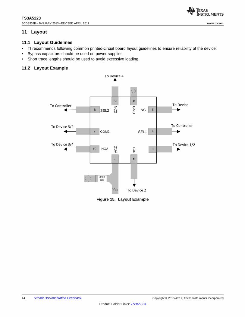
11 Layout
11.1 Layout Guidelines• TI recommends following common printed-circuit board layout guidelines to ensure reliability of the device.• Bypass capacitors should be used on power supplies.• Short trace lengths should be used to avoid excessive loading.
11.2 Layout Example
Figure 15. Layout Example
15
TS3A5223www.ti.com SCDS339B –JANUARY 2013–REVISED APRIL 2017
Product Folder Links: TS3A5223
Submit Documentation FeedbackCopyright © 2013–2017, Texas Instruments Incorporated
12 Device and Documentation Support
12.1 Documentation Support
12.2 Receiving Notification of Documentation UpdatesTo receive notification of documentation updates, navigate to the device product folder on ti.com. In the upperright corner, click on Alert me to register and receive a weekly digest of any product information that haschanged. For change details, review the revision history included in any revised document.
12.3 Community ResourcesThe following links connect to TI community resources. Linked contents are provided "AS IS" by the respectivecontributors. They do not constitute TI specifications and do not necessarily reflect TI's views; see TI's Terms ofUse.
TI E2E™ Online Community TI's Engineer-to-Engineer (E2E) Community. Created to foster collaborationamong engineers. At e2e.ti.com, you can ask questions, share knowledge, explore ideas and helpsolve problems with fellow engineers.
Design Support TI's Design Support Quickly find helpful E2E forums along with design support tools andcontact information for technical support.
12.4 TrademarksE2E is a trademark of Texas Instruments.
12.5 Electrostatic Discharge CautionThis integrated circuit can be damaged by ESD. Texas Instruments recommends that all integrated circuits be handled withappropriate precautions. Failure to observe proper handling and installation procedures can cause damage.
ESD damage can range from subtle performance degradation to complete device failure. Precision integrated circuits may be moresusceptible to damage because very small parametric changes could cause the device not to meet its published specifications.
12.6 GlossarySLYZ022 — TI Glossary.
This glossary lists and explains terms, acronyms, and definitions.
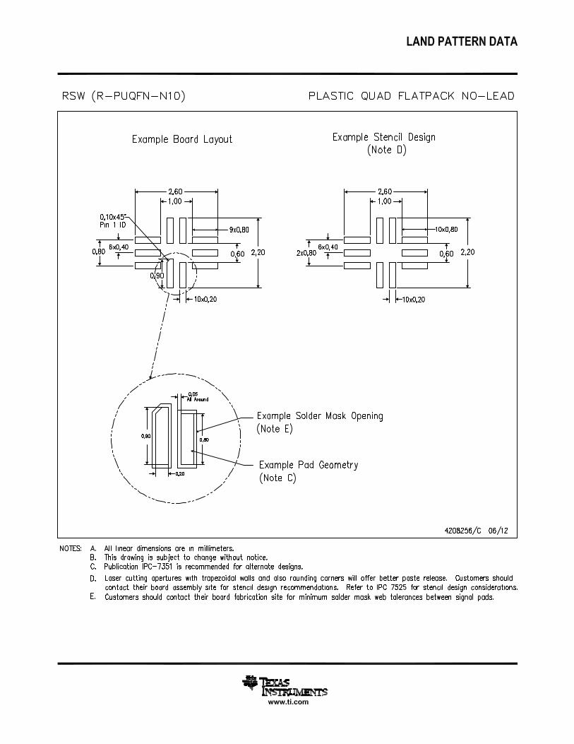
13 Mechanical, Packaging, and Orderable InformationThe following pages include mechanical, packaging, and orderable information. This information is the mostcurrent data available for the designated devices. This data is subject to change without notice and revision ofthis document. For browser-based versions of this data sheet, refer to the left-hand navigation.
PACKAGE OPTION ADDENDUM
www.ti.com 23-Mar-2017
Addendum-Page 1
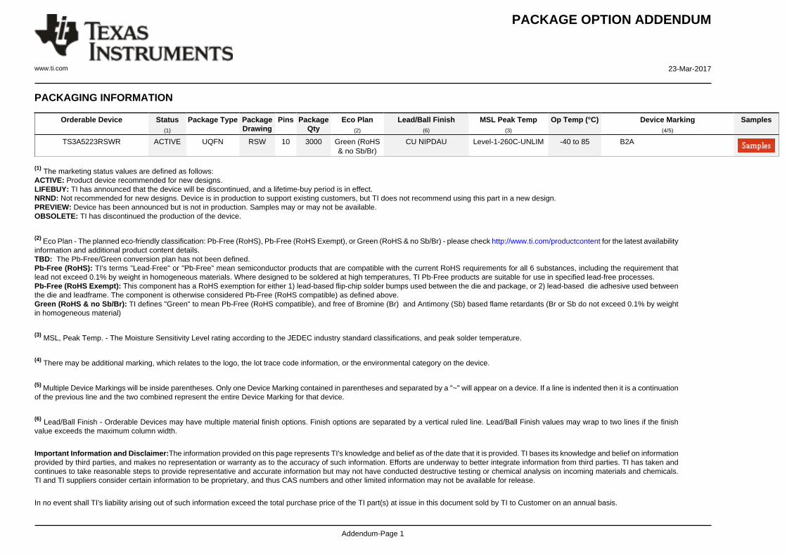
PACKAGING INFORMATION
Orderable Device Status(1)
Package Type PackageDrawing
Pins PackageQty
Eco Plan(2)
Lead/Ball Finish(6)
MSL Peak Temp(3)
Op Temp (°C) Device Marking(4/5)
Samples
TS3A5223RSWR ACTIVE UQFN RSW 10 3000 Green (RoHS& no Sb/Br)
CU NIPDAU Level-1-260C-UNLIM -40 to 85 B2A
(1) The marketing status values are defined as follows:ACTIVE: Product device recommended for new designs.LIFEBUY: TI has announced that the device will be discontinued, and a lifetime-buy period is in effect.NRND: Not recommended for new designs. Device is in production to support existing customers, but TI does not recommend using this part in a new design.PREVIEW: Device has been announced but is not in production. Samples may or may not be available.OBSOLETE: TI has discontinued the production of the device.
(2) Eco Plan - The planned eco-friendly classification: Pb-Free (RoHS), Pb-Free (RoHS Exempt), or Green (RoHS & no Sb/Br) - please check http://www.ti.com/productcontent for the latest availabilityinformation and additional product content details.TBD: The Pb-Free/Green conversion plan has not been defined.Pb-Free (RoHS): TI's terms "Lead-Free" or "Pb-Free" mean semiconductor products that are compatible with the current RoHS requirements for all 6 substances, including the requirement thatlead not exceed 0.1% by weight in homogeneous materials. Where designed to be soldered at high temperatures, TI Pb-Free products are suitable for use in specified lead-free processes.Pb-Free (RoHS Exempt): This component has a RoHS exemption for either 1) lead-based flip-chip solder bumps used between the die and package, or 2) lead-based die adhesive used betweenthe die and leadframe. The component is otherwise considered Pb-Free (RoHS compatible) as defined above.Green (RoHS & no Sb/Br): TI defines "Green" to mean Pb-Free (RoHS compatible), and free of Bromine (Br) and Antimony (Sb) based flame retardants (Br or Sb do not exceed 0.1% by weightin homogeneous material)
(3) MSL, Peak Temp. - The Moisture Sensitivity Level rating according to the JEDEC industry standard classifications, and peak solder temperature.
(4) There may be additional marking, which relates to the logo, the lot trace code information, or the environmental category on the device.
(5) Multiple Device Markings will be inside parentheses. Only one Device Marking contained in parentheses and separated by a "~" will appear on a device. If a line is indented then it is a continuationof the previous line and the two combined represent the entire Device Marking for that device.
(6) Lead/Ball Finish - Orderable Devices may have multiple material finish options. Finish options are separated by a vertical ruled line. Lead/Ball Finish values may wrap to two lines if the finishvalue exceeds the maximum column width.
Important Information and Disclaimer:The information provided on this page represents TI's knowledge and belief as of the date that it is provided. TI bases its knowledge and belief on informationprovided by third parties, and makes no representation or warranty as to the accuracy of such information. Efforts are underway to better integrate information from third parties. TI has taken andcontinues to take reasonable steps to provide representative and accurate information but may not have conducted destructive testing or chemical analysis on incoming materials and chemicals.TI and TI suppliers consider certain information to be proprietary, and thus CAS numbers and other limited information may not be available for release.
In no event shall TI's liability arising out of such information exceed the total purchase price of the TI part(s) at issue in this document sold by TI to Customer on an annual basis.
PACKAGE OPTION ADDENDUM
www.ti.com 23-Mar-2017
Addendum-Page 2
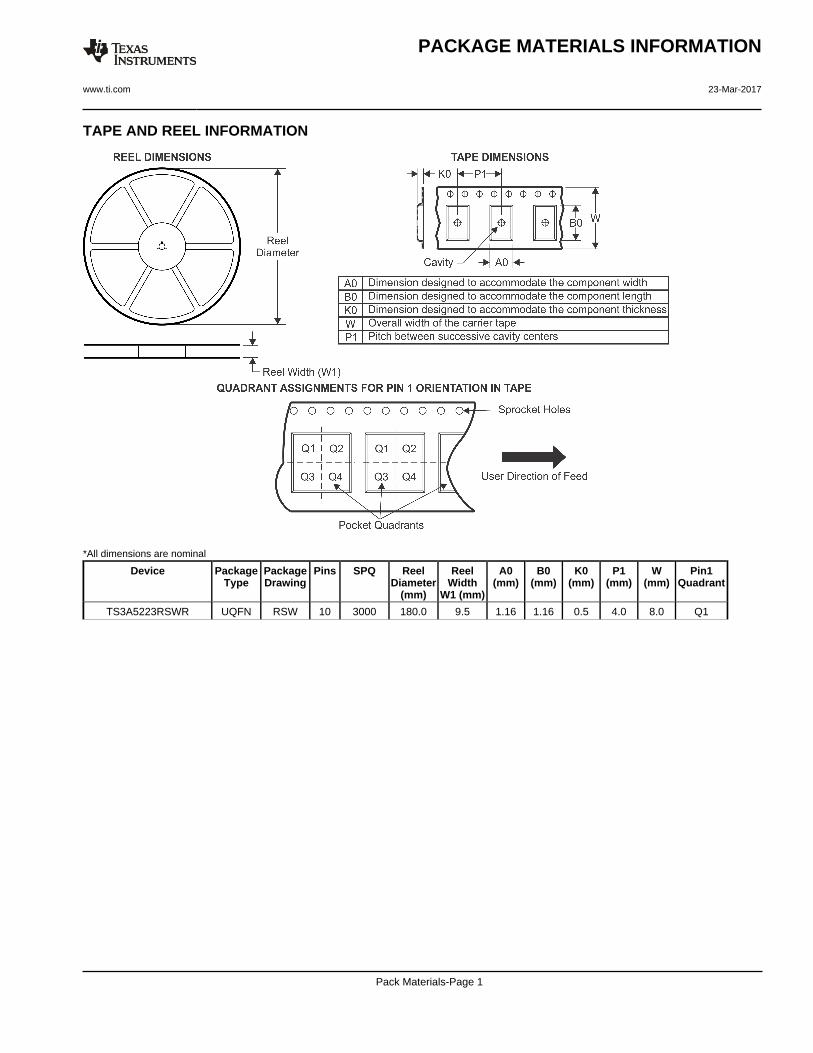
TAPE AND REEL INFORMATION
*All dimensions are nominal
Device PackageType
PackageDrawing
Pins SPQ ReelDiameter
(mm)
ReelWidth
W1 (mm)
A0(mm)
B0(mm)
K0(mm)
P1(mm)
W(mm)
Pin1Quadrant
TS3A5223RSWR UQFN RSW 10 3000 180.0 9.5 1.16 1.16 0.5 4.0 8.0 Q1
PACKAGE MATERIALS INFORMATION
www.ti.com 23-Mar-2017
Pack Materials-Page 1
*All dimensions are nominal
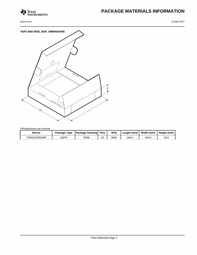
Device Package Type Package Drawing Pins SPQ Length (mm) Width (mm) Height (mm)
TS3A5223RSWR UQFN RSW 10 3000 184.0 184.0 19.0
PACKAGE MATERIALS INFORMATION
www.ti.com 23-Mar-2017
Pack Materials-Page 2
IMPORTANT NOTICE
Texas Instruments Incorporated (TI) reserves the right to make corrections, enhancements, improvements and other changes to itssemiconductor products and services per JESD46, latest issue, and to discontinue any product or service per JESD48, latest issue. Buyersshould obtain the latest relevant information before placing orders and should verify that such information is current and complete.TI’s published terms of sale for semiconductor products (http://www.ti.com/sc/docs/stdterms.htm) apply to the sale of packaged integratedcircuit products that TI has qualified and released to market. Additional terms may apply to the use or sale of other types of TI products andservices.Reproduction of significant portions of TI information in TI data sheets is permissible only if reproduction is without alteration and isaccompanied by all associated warranties, conditions, limitations, and notices. TI is not responsible or liable for such reproduceddocumentation. Information of third parties may be subject to additional restrictions. Resale of TI products or services with statementsdifferent from or beyond the parameters stated by TI for that product or service voids all express and any implied warranties for theassociated TI product or service and is an unfair and deceptive business practice. TI is not responsible or liable for any such statements.Buyers and others who are developing systems that incorporate TI products (collectively, “Designers”) understand and agree that Designersremain responsible for using their independent analysis, evaluation and judgment in designing their applications and that Designers havefull and exclusive responsibility to assure the safety of Designers' applications and compliance of their applications (and of all TI productsused in or for Designers’ applications) with all applicable regulations, laws and other applicable requirements. Designer represents that, withrespect to their applications, Designer has all the necessary expertise to create and implement safeguards that (1) anticipate dangerousconsequences of failures, (2) monitor failures and their consequences, and (3) lessen the likelihood of failures that might cause harm andtake appropriate actions. Designer agrees that prior to using or distributing any applications that include TI products, Designer willthoroughly test such applications and the functionality of such TI products as used in such applications.TI’s provision of technical, application or other design advice, quality characterization, reliability data or other services or information,including, but not limited to, reference designs and materials relating to evaluation modules, (collectively, “TI Resources”) are intended toassist designers who are developing applications that incorporate TI products; by downloading, accessing or using TI Resources in anyway, Designer (individually or, if Designer is acting on behalf of a company, Designer’s company) agrees to use any particular TI Resourcesolely for this purpose and subject to the terms of this Notice.TI’s provision of TI Resources does not expand or otherwise alter TI’s applicable published warranties or warranty disclaimers for TIproducts, and no additional obligations or liabilities arise from TI providing such TI Resources. TI reserves the right to make corrections,enhancements, improvements and other changes to its TI Resources. TI has not conducted any testing other than that specificallydescribed in the published documentation for a particular TI Resource.Designer is authorized to use, copy and modify any individual TI Resource only in connection with the development of applications thatinclude the TI product(s) identified in such TI Resource. NO OTHER LICENSE, EXPRESS OR IMPLIED, BY ESTOPPEL OR OTHERWISETO ANY OTHER TI INTELLECTUAL PROPERTY RIGHT, AND NO LICENSE TO ANY TECHNOLOGY OR INTELLECTUAL PROPERTYRIGHT OF TI OR ANY THIRD PARTY IS GRANTED HEREIN, including but not limited to any patent right, copyright, mask work right, orother intellectual property right relating to any combination, machine, or process in which TI products or services are used. Informationregarding or referencing third-party products or services does not constitute a license to use such products or services, or a warranty orendorsement thereof. Use of TI Resources may require a license from a third party under the patents or other intellectual property of thethird party, or a license from TI under the patents or other intellectual property of TI.TI RESOURCES ARE PROVIDED “AS IS” AND WITH ALL FAULTS. TI DISCLAIMS ALL OTHER WARRANTIES ORREPRESENTATIONS, EXPRESS OR IMPLIED, REGARDING RESOURCES OR USE THEREOF, INCLUDING BUT NOT LIMITED TOACCURACY OR COMPLETENESS, TITLE, ANY EPIDEMIC FAILURE WARRANTY AND ANY IMPLIED WARRANTIES OFMERCHANTABILITY, FITNESS FOR A PARTICULAR PURPOSE, AND NON-INFRINGEMENT OF ANY THIRD PARTY INTELLECTUALPROPERTY RIGHTS. TI SHALL NOT BE LIABLE FOR AND SHALL NOT DEFEND OR INDEMNIFY DESIGNER AGAINST ANY CLAIM,INCLUDING BUT NOT LIMITED TO ANY INFRINGEMENT CLAIM THAT RELATES TO OR IS BASED ON ANY COMBINATION OFPRODUCTS EVEN IF DESCRIBED IN TI RESOURCES OR OTHERWISE. IN NO EVENT SHALL TI BE LIABLE FOR ANY ACTUAL,DIRECT, SPECIAL, COLLATERAL, INDIRECT, PUNITIVE, INCIDENTAL, CONSEQUENTIAL OR EXEMPLARY DAMAGES INCONNECTION WITH OR ARISING OUT OF TI RESOURCES OR USE THEREOF, AND REGARDLESS OF WHETHER TI HAS BEENADVISED OF THE POSSIBILITY OF SUCH DAMAGES.Unless TI has explicitly designated an individual product as meeting the requirements of a particular industry standard (e.g., ISO/TS 16949and ISO 26262), TI is not responsible for any failure to meet such industry standard requirements.Where TI specifically promotes products as facilitating functional safety or as compliant with industry functional safety standards, suchproducts are intended to help enable customers to design and create their own applications that meet applicable functional safety standardsand requirements. Using products in an application does not by itself establish any safety features in the application. Designers mustensure compliance with safety-related requirements and standards applicable to their applications. Designer may not use any TI products inlife-critical medical equipment unless authorized officers of the parties have executed a special contract specifically governing such use.Life-critical medical equipment is medical equipment where failure of such equipment would cause serious bodily injury or death (e.g., lifesupport, pacemakers, defibrillators, heart pumps, neurostimulators, and implantables). Such equipment includes, without limitation, allmedical devices identified by the U.S. Food and Drug Administration as Class III devices and equivalent classifications outside the U.S.TI may expressly designate certain products as completing a particular qualification (e.g., Q100, Military Grade, or Enhanced Product).Designers agree that it has the necessary expertise to select the product with the appropriate qualification designation for their applicationsand that proper product selection is at Designers’ own risk. Designers are solely responsible for compliance with all legal and regulatoryrequirements in connection with such selection.Designer will fully indemnify TI and its representatives against any damages, costs, losses, and/or liabilities arising out of Designer’s non-compliance with the terms and provisions of this Notice.
Mailing Address: Texas Instruments, Post Office Box 655303, Dallas, Texas 75265Copyright © 2017, Texas Instruments Incorporated