transition-edge sensors for precision measurements from … · transition-edge sensors for...
35
transition-edge sensors for precision measurements from γ-ray to submm wavelengths Joel Ullom, NIST Boulder NIST Boulder: James Beall Randy Doriese William Duncan Lisa Ferreira Gene Hilton Rob Horansky Kent Irwin Ben Mates Nathan Miller Galen O’Neil Carl Reintsema Dan Schmidt Leila Vale Yizi Xu NIST Gaithersburg: Dale Newbury Terry Jach Nicholas Ritchie John Small
Transcript of transition-edge sensors for precision measurements from … · transition-edge sensors for...

transition-edge sensors forprecision measurements from γ-ray to submm
wavelengths
Joel Ullom, NIST Boulder
NIST Boulder:James Beall
Randy DorieseWilliam Duncan
Lisa FerreiraGene Hilton
Rob HoranskyKent IrwinBen Mates
Nathan MillerGalen O’Neil
Carl ReintsemaDan SchmidtLeila ValeYizi Xu
NIST Gaithersburg:Dale NewburyTerry JachNicholas RitchieJohn Small

Thermal sensors
Tem
pera
ture
Time
CE
CGτ =
S. H. Moseley, J. Mather and D. McCammon, J. Appl. Phys., 56: 1257 (1984)
energy (calorimeter)or
power (bolometer)
ConductanceG ThermalC
HeatCapacity
• Noise source: power fluctuations PN in thermal conductance: (4kbT2G)1/2 W/Hz1/2
• For calorimeters, ∆E = PN * τ * (bandwidth)1/2 ~ (4kbT2G)1/2 * (C/G)1/2 ~ (kbT2C)1/2 J
• So, sensor performance best at low temperatures:At 0.1 K, C = 1 pJ/K, G = 1 nW/K reasonable
NEP = 2 * 10-17 W/Hz1/2 , ∆E = 2 eV

Simple 100 mK cryogenics
ADR and cryogen vesselsmounted on SEM
NIST 2-stage ADR -licensed and now availablecommercially
2-stage adiabaticdemagnetization refrigerator(ADR)

330 mm
Getting to 4 Kelvin
• Traditionally, use LN2 and LHe• expensive (LHe = $5/liter)• requires skilled users• explosion risk• not suitable for field use
• More recently, mechanical cryocoolers: perform thermodynamic cycle on sealed working gas (He)
• push-button operation• only consumable = electricity• some vibration signature
pulse tube cryocooler
300 K
2.7 K
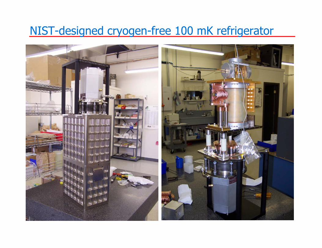
NIST-designed cryogen-free 100 mK refrigerator

Superconducting Transition-Edge Sensor (TES) thermometer
• Transition-Edge Sensor (TES) = thin-film biased in superconducting-normal transition
• Use strong dR/dT in transition as thermometer
• Historically, the TES was too sensitive: difficult to temperature bias, and low count rate. This was fixed by the introduction of voltage biasing and electrothermal feedback.
0.02
0.04
0.06
095.8 96 96.2
Temperature (mK)
Res
ista
nce
(Ω)
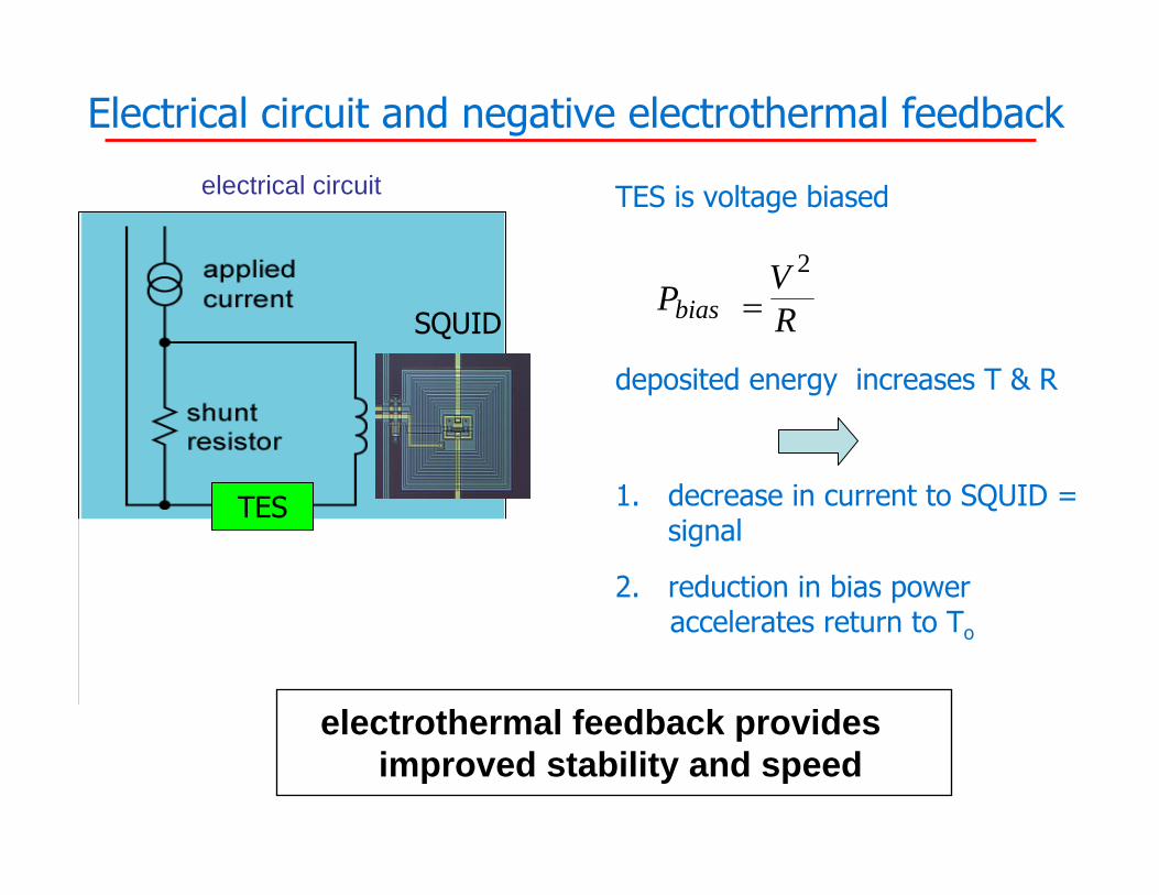
TES is voltage biased
deposited energy increases T & R
1. decrease in current to SQUID = signal
2. reduction in bias power accelerates return to To
Electrical circuit and negative electrothermal feedback
electrical circuit
RVPbias
2
=SQUID
TES
electrothermal feedback providesimproved stability and speed
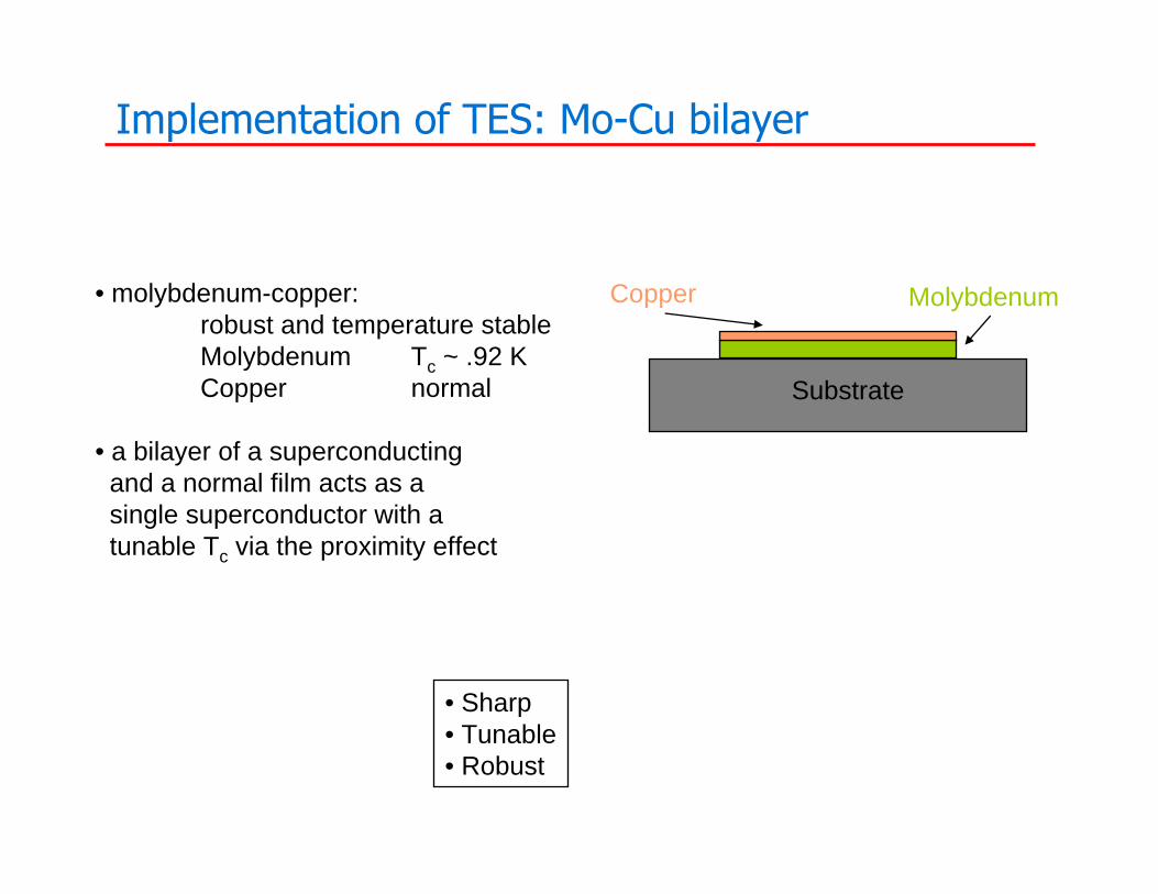
Implementation of TES: Mo-Cu bilayer
• molybdenum-copper:robust and temperature stableMolybdenum Tc ~ .92 KCopper normal
• a bilayer of a superconducting and a normal film acts as asingle superconductor with atunable Tc via the proximity effect
• Sharp• Tunable• Robust
Copper Molybdenum
Substrate
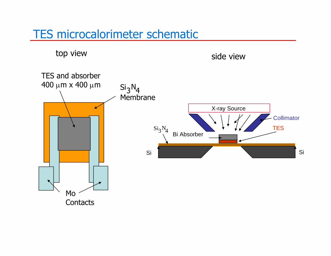
TES microcalorimeter schematic
MoContacts
TES and absorber400 µm x 400 µm Si
Membrane43N
X-ray Source
Si Si
Bi AbsorberTES
Collimator
Si 43N
top view side view

X-ray application #1: materials analysis• x-ray spectroscopy is a powerful tool for materials analysis
• commonly performed on scanning electron microscopes (SEMs) and at synchrotrons
• existing technologies:semiconductor EDS
- ubiquitous- large collecting areas and count rates- but resolution ~ 100 eV
WDS- high resolution- but smaller collecting area & broad-band operation complicated
• cryogenic microcalorimeters combine advantages of EDS and WDS:- broad-band (500 eV - 10 keV easy)- high resolution (few eV)- moderate collecting area

Microcalorimeters for materials analysis
500 1000 1500 20000
500
1000
1500
2000NISTµcal EDS
C Kα
O Kα
Fe LαNi Lα
Zn Lα
Mg KαAl Kα
Si Kα
µcal
ED
S C
ount
s (0.
16eV
bin
s)
Energy (eV)0
5000
10000
15000
(real-time analog processing)
NIST K3670 glassSi(Li) EDS
Si(L
i) ED
S C
ount
s (10
eV b
ins)
adiabatic demagnetization refrigerator & microcalorimeter mounted on SEM: units at Boulder & Gaithersburg
microcalorimeter and Si(Li)spectra of reference glass
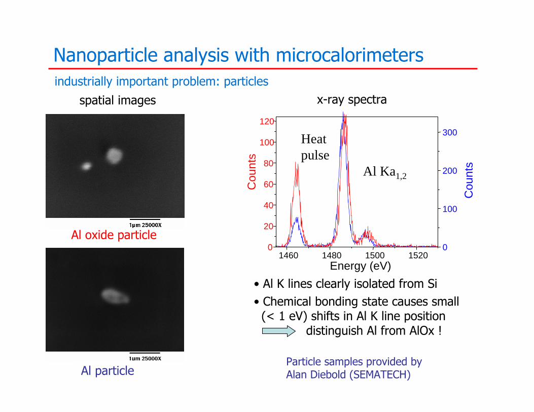
Nanoparticle analysis with microcalorimeters
Al oxide particle
Al Ka1,2
1460 1480 1500 15200
20
40
60
80
100
120
0
100
200
300
Co
un
ts
Co
un
tsEnergy (eV)
Heatpulse
Al particle
• Al K lines clearly isolated from Si• Chemical bonding state causes small
(< 1 eV) shifts in Al K line positiondistinguish Al from AlOx !
Particle samples provided by Alan Diebold (SEMATECH)
spatial images x-ray spectraindustrially important problem: particles
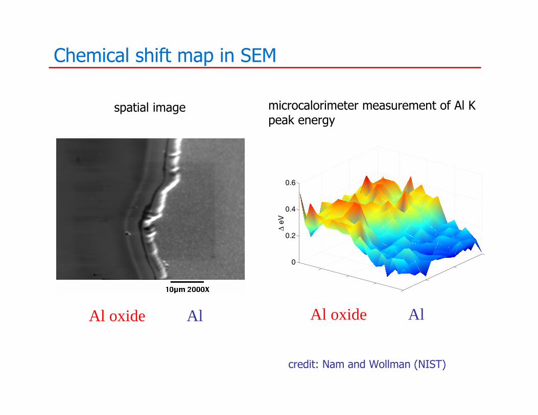
Chemical shift map in SEM
0
0.2
0.4
0.6
∆ eV
Al oxide Al
spatial image microcalorimeter measurement of Al K peak energy
Al oxide Al
credit: Nam and Wollman (NIST)
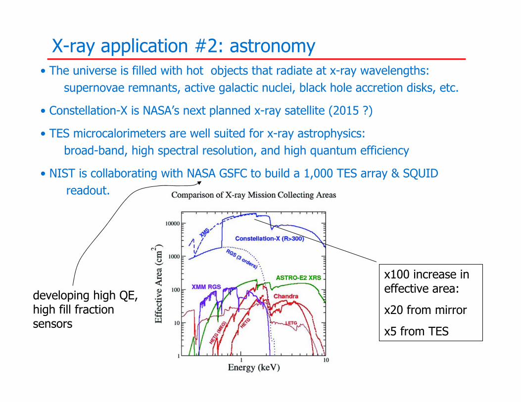
• The universe is filled with hot objects that radiate at x-ray wavelengths:supernovae remnants, active galactic nuclei, black hole accretion disks, etc.
• Constellation-X is NASA’s next planned x-ray satellite (2015 ?)
• TES microcalorimeters are well suited for x-ray astrophysics: broad-band, high spectral resolution, and high quantum efficiency
• NIST is collaborating with NASA GSFC to build a 1,000 TES array & SQUIDreadout.
X-ray application #2: astronomy
x100 increase in effective area:
x20 from mirror
x5 from TES
developing high QE, high fill fractionsensors
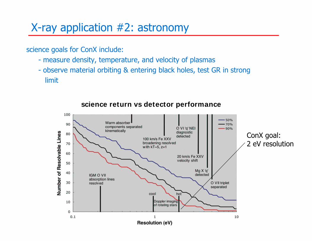
science goals for ConX include:- measure density, temperature, and velocity of plasmas- observe material orbiting & entering black holes, test GR in strong
limit
X-ray application #2: astronomy
science return vs detector performance
ConX goal:2 eV resolution
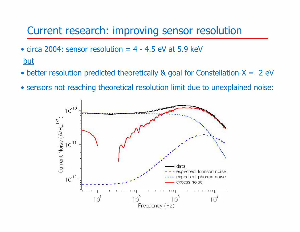
Current research: improving sensor resolution
• circa 2004: sensor resolution = 4 - 4.5 eV at 5.9 keV
but
• better resolution predicted theoretically & goal for Constellation-X = 2 eV
• sensors not reaching theoretical resolution limit due to unexplained noise:

Effects of geometry
additional normal metal features
how does noise scale with geometry ?

Noise vs. geometry: unexplained noise and α correlated
• low α designs have little unexplained noise• perpendicular normal features reduce noise and α
all data at 60% RN
7
6
5
4
3
2
1
0
Unex
plai
ned
Noi
se/J
ohns
on N
oise
10008006004002000α
standard
parallel& perp
sparsepartial perp
densepartial perp
wedge
dense parallel
islands standard #2
densefull perp
transition sharpness ‘α’
unexplained noise ‘M’

Optimized TES: energy resolution = 2.4 eV FWHM at 5.9 keV
• integrated into close-packed array• 1.5 µm Bi absorber QE ~ 55% at 5.9 keV• 260 µs decay time
useful device:
7,754 counts
best resolution of any energy-dispersive detector at 6 keV

TES arrays
array schematic
• use deep reactive ion etching (DRIE) to remove substrate beneath pixels & achieve necessary thermal isolation
• use remaining Si beams for wiring, indium bumps, or through-wafer vias
64 pixel x-ray array
6.25 mm

Readout of large sensor arrays
concept implementation
use time-domain SQUID multiplexing:
• 1 amplifier chain/column of sensors
• amplifier chain = 3 SQUID stages
• stages 2 & 3 shared between sensors of column
• each sensor has own squid (stage 1), usedas switch
sensors stage 1 stage 2 stage 3
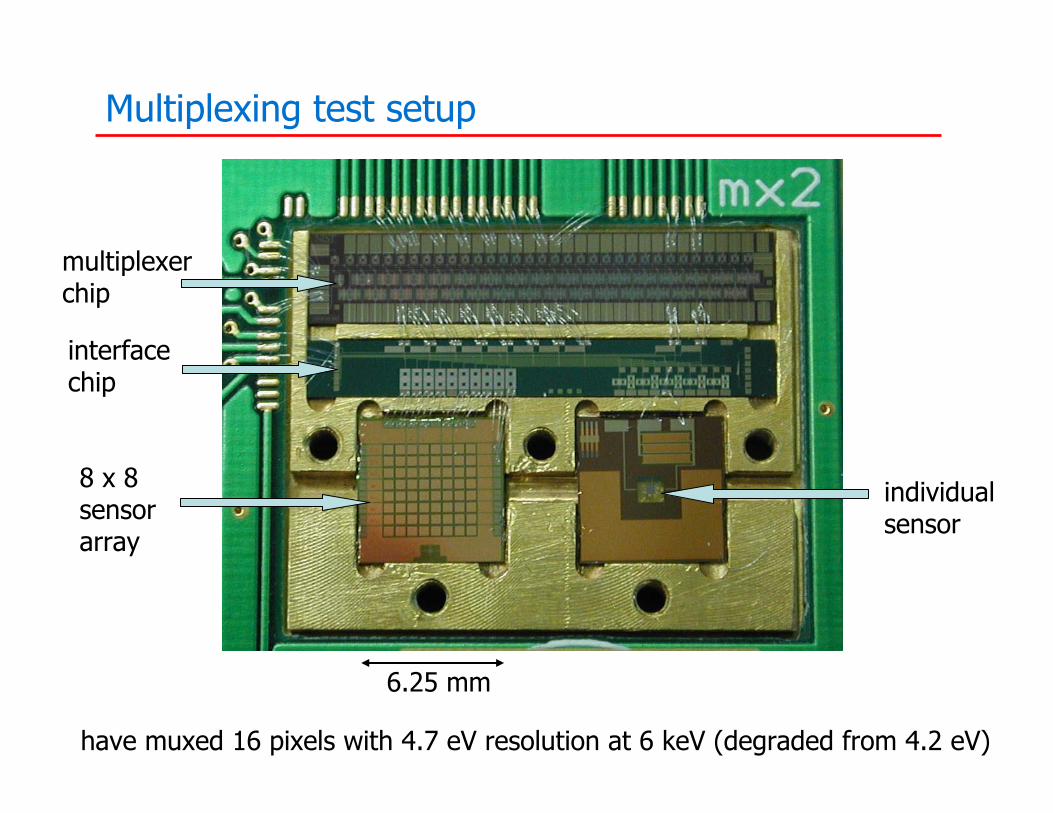
Multiplexing test setup
6.25 mm
interfacechip
multiplexerchip
8 x 8 sensorarray
individualsensor
have muxed 16 pixels with 4.7 eV resolution at 6 keV (degraded from 4.2 eV)
1 mm
160
120
80
40
0103.30103.25103.20103.15103.10103.05
42 eV FWHM
140
120
100
80
60
40
20
0
Cou
nts
/ 5 e
V b
in
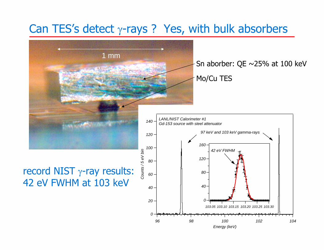
1041021009896Energy (keV)
LANL/NIST Calorimeter #1Gd-153 source with steel attenuator
97 keV and 103 keV gamma-rays
Sn aborber: QE ~25% at 100 keV
Mo/Cu TES
record NIST γ-ray results: 42 eV FWHM at 103 keV
Can TES’s detect γ-rays ? Yes, with bulk absorbers

LANL-NIST Pu spectrum: isotopes clearly resolved
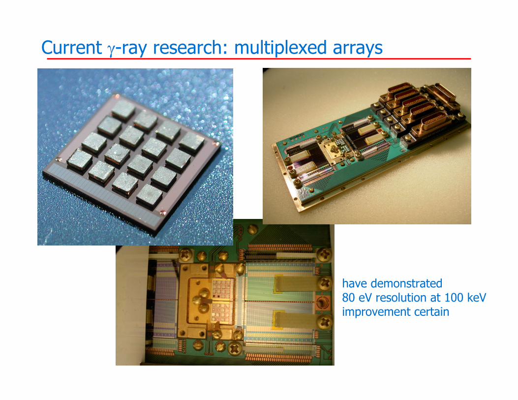
Current γ-ray research: multiplexed arrays
have demonstrated80 eV resolution at 100 keVimprovement certain

SCUBA 2 - TES sensors for submm astronomy• The James-Clark Maxwell Telescope (JCMT) is one of the largest sub-millimeter telescopes
in the world.
• The primary scientific instrument on the JCMT is the SCUBA bolometer array consisting of~ 130 pixels. SCUBA is a very successfully, heavily cited instrument.
• NIST is a partner in an international collaboration to build SCUBA-2 which will be 102 -103
times more powerful than SCUBA. (with UK ATC, Edinburgh, Cardiff, Raytheon, Canada … )
JCMT on Mauna Kea
SCUBA imageof supernovaremnant Cass APhysics Today,Oct. 2003
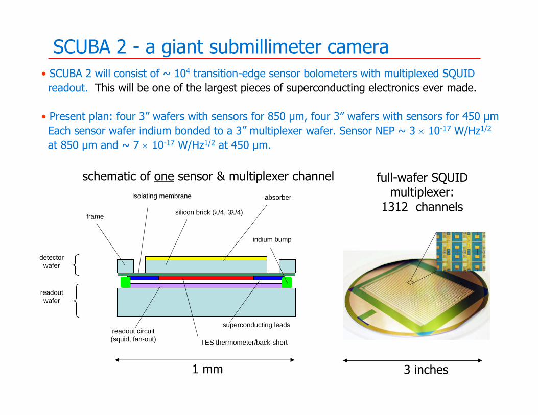
SCUBA 2 - a giant submillimeter camera
detectorwafer
readoutwafer
absorber
silicon brick (λ/4, 3λ/4)
isolating membrane
readout circuit(squid, fan-out) TES thermometer/back-short
indium bump
superconducting leads
frame
full-wafer SQUIDmultiplexer:
1312 channels
• SCUBA 2 will consist of ~ 104 transition-edge sensor bolometers with multiplexed SQUIDreadout. This will be one of the largest pieces of superconducting electronics ever made.
• Present plan: four 3” wafers with sensors for 850 µm, four 3” wafers with sensors for 450 µmEach sensor wafer indium bonded to a 3” multiplexer wafer. Sensor NEP ~ 3 × 10-17 W/Hz1/2
at 850 µm and ~ 7 × 10-17 W/Hz1/2 at 450 µm.
1 mm 3 inches
schematic of one sensor & multiplexer channel
3 inches
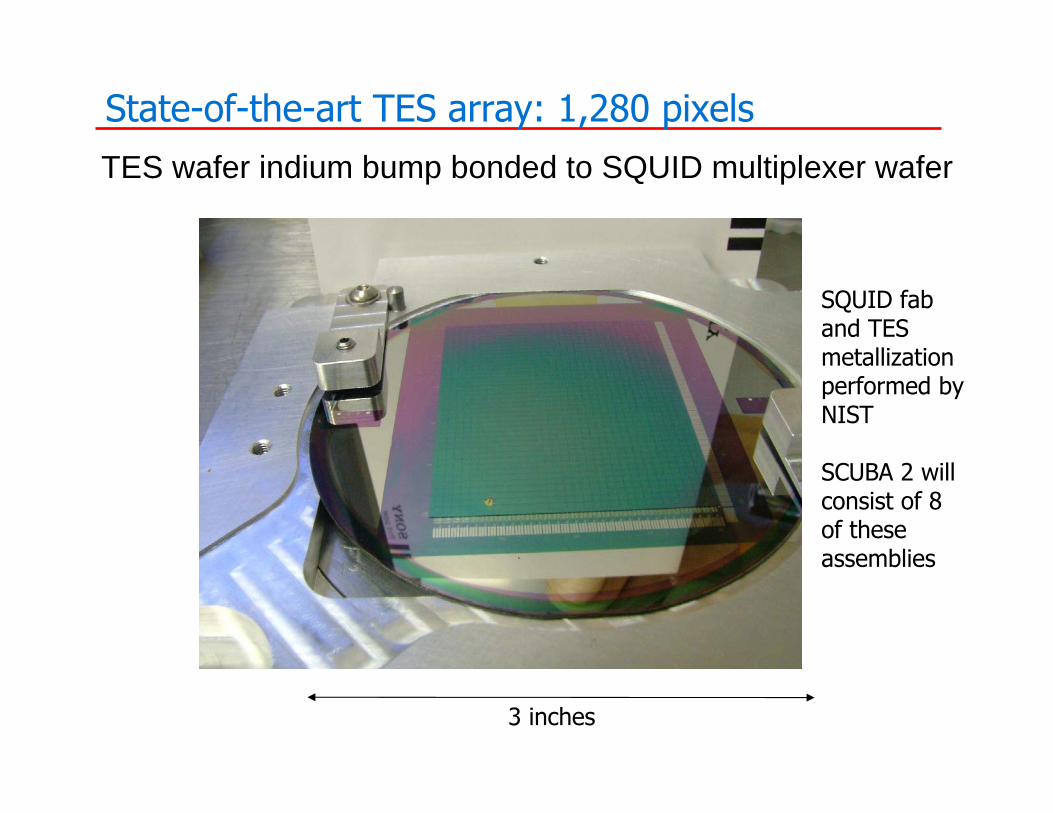
State-of-the-art TES array: 1,280 pixelsTES wafer indium bump bonded to SQUID multiplexer wafer
SQUID fab and TES metallization performed by NIST
SCUBA 2 willconsist of 8of these assemblies

Development possible over 5-10 years
5 - 10 years
100 MHz100,0005 eV0.1 – 10 keVMicrowavereadout
TimescaleArray count
ratearray size∆EFWHMEOptimization
~ 5 years20 MHz100 ×100
6 eV0.1 – 1 keVBest count rate 1 keV
0.1 – 10 keV
0.1 – 10 keV
100 ×100
32 × 32
~ 5 years5 MHz20 eVBest count rate 10 keV
~ 3 years200 kHz3 eVBest resolution
Can also make instruments for THz, IR, visible, UV, & γ-ray
Future prospects
x-ray detectors = most challenging: need speed and resolution
Conclusions
• 0.1 K operating temperatures now achievable simply and without liquid cryogens
• performance of individual TES sensors = excellent- 2.0 eV FWHM at 1.5 keV- 2.4 eV at 5.9 keV- 42 eV at 103 keV- 1/e response time = 100 µs - 1 ms- area = 0.1 - 1 mm2
• TESs well suited for terrestrial materials analysis (x- and γ-ray) and astronomy (x-ray and submm)
• we are now building and testing arrays of x-ray, γ-ray, and submm TESs
• multiplexing = essential for arrays, time-domain SQUID mux works well
• SCUBA 2 submm camera (104 sensors) underway


• Low electron beam energies required to probe small or thin samples
• BUT, low energy electrons only excite low energy x-rays peak overlap
• Microcalorimeters can easily resolve overlap
Nanoscale Analysis with Microcalorimeters
Low beam energy; x-rays from particle
High beam energy; x-rays from substrate
e- e-x-ray
x-ray

Can TESs measure γ-rays ?
QE of thin-film devices too low (≤ 1%)
BUT, there is a simple solution:
attach a bulk absorber to the TESγ-ray energy is captured, thermalized in absorberenergy flows from absorber into TES
need low C absorber; candidate materials = insulators & superconductors
glueTES
SiN membrane
Sn absorber‘bulk’ Sn:1 x 1 x 0.25 mm3
QE = 24% at 100 keV
Cabs = 60 keV/mK
CTES = 9 keV/mK
but volume ratio = 1250
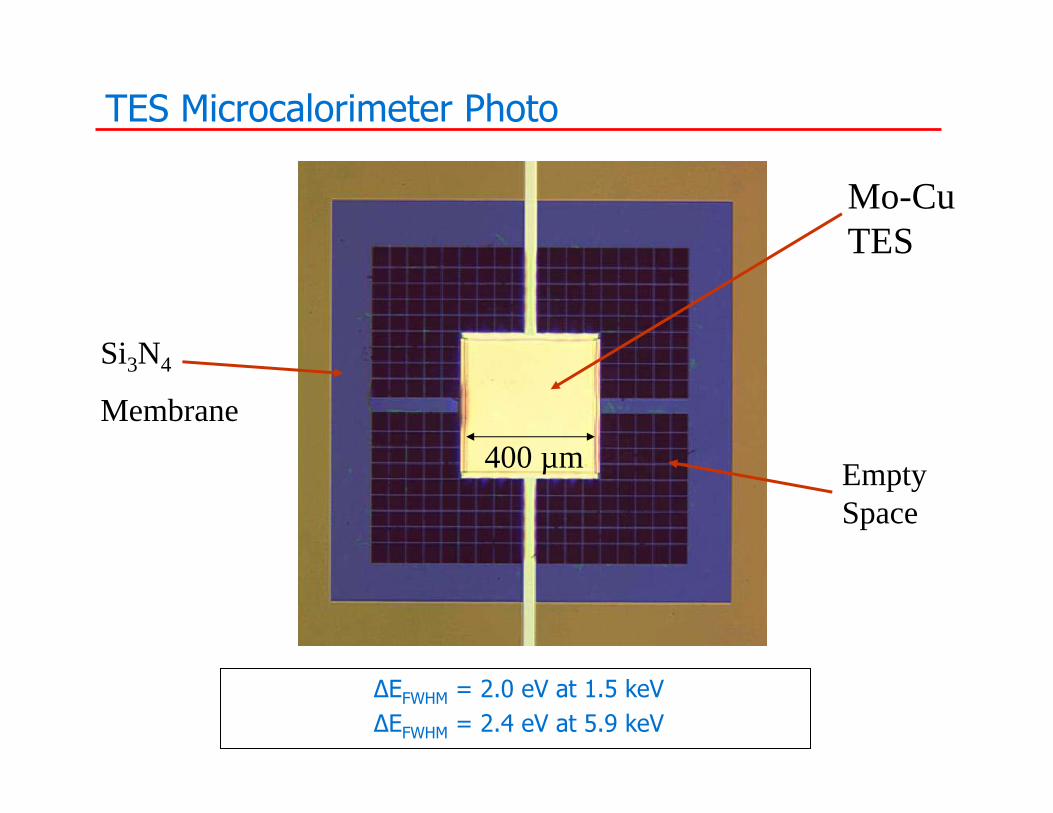
TES Microcalorimeter Photo
Mo-Cu TES
EmptySpace
Si3N4
Membrane400 µm
∆EFWHM = 2.0 eV at 1.5 keV∆EFWHM = 2.4 eV at 5.9 keV

TES Optimization
∆E FWHM = 2.35
4kbT2C
αn (1 +M2)
2 M is excess noise
ratioed to Johnson noise
empirically, M ~ 0.2 α1/2 lower α to lower excess noise
optimal design: reduce C, α, and M, match C/α to target x-ray energy
additional constraint: Esaturation ~ C T/α