
NTEGRA spectra: Cutting edge of molecular sciences
34
NTEGRA spectra: Cutting edge of molecular sciences
Transcript of NTEGRA spectra: Cutting edge of molecular sciences

NTEGRA spectra:Cutting edge of molecular sciences
Raman spectroscopy at the nanometer scaleNTEGRA spectra key featuresApplications
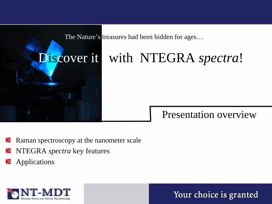
The Nature’s treasures had been hidden for ages…
Discover it with NTEGRA spectra!
Presentation overview
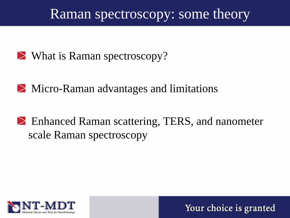
Raman spectroscopy: some theory
What is Raman spectroscopy?
Micro-Raman advantages and limitations
Enhanced Raman scattering, TERS, and nanometer scale Raman spectroscopy
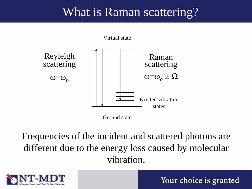
What is Raman scattering?
Ground state
Virtual state
Reyleighscatteringω=ωo
Raman scatteringω=ωo ± Ω
Frequencies of the incident and scattered photons are different due to the energy loss caused by molecular
vibration.
Excited vibration states
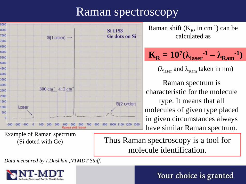
Raman spectroscopyRaman shift (KR, in cm-1) can be
calculated as
KR = 107(λlaser-1 – λRam
-1) (λlaser and λRam taken in nm)
Example of Raman spectrum (Si doted with Ge)
Raman spectrum is characteristic for the molecule
type. It means that all molecules of given type placed in given circumstances always have similar Raman spectrum.
Thus Raman spectroscopy is a tool for molecule identification.
Data measured by I.Dushkin ,NTMDT Staff.
Where is Raman spectroscopy among other methods?
As a tool for characterization of chemical composition Raman spectroscopy is very close to IR-spectroscopy. These
are complementary techniques. For example, symmetric stretch of CO2 molecule is not visible in IR-spectrum but it is
visible in Raman spectrum.
Comprehensive libraries of IR and Raman spectra had been collected for almost all known substances in most states and
different environments for many decades of 20th century.
Micro-Raman: Spectroscopy and imaging
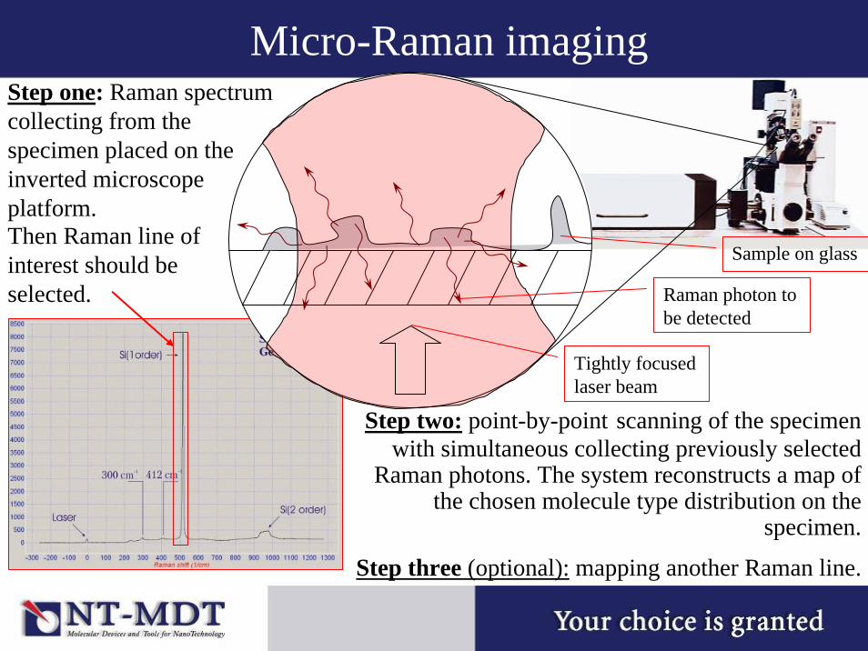
Micro-Raman imaging
Tightly focused laser beam
Sample on glass
Raman photon to be detected
Step one: Raman spectrum collecting from the specimen placed on the inverted microscope platform. Then Raman line of interest should be selected.
Step two: point-by-point scanning of the specimen with simultaneous collecting previously selected
Raman photons. The system reconstructs a map of the chosen molecule type distribution on the
specimen.
Step three (optional): mapping another Raman line.
Raman imaging
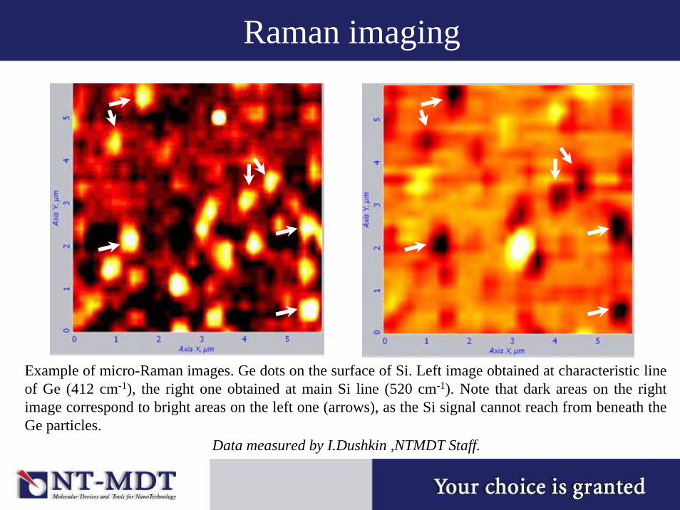
Example of micro-Raman images. Ge dots on the surface of Si. Left image obtained at characteristic line of Ge (412 cm-1), the right one obtained at main Si line (520 cm-1). Note that dark areas on the right image correspond to bright areas on the left one (arrows), as the Si signal cannot reach from beneath the Ge particles.
Data measured by I.Dushkin ,NTMDT Staff.
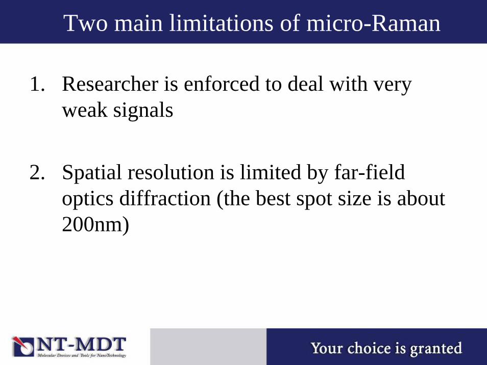
Two main limitations of micro-Raman
1. Researcher is enforced to deal with very weak signals
2. Spatial resolution is limited by far-field optics diffraction (the best spot size is about 200nm)

Enhanced Raman scattering
TERS – Tip Enhanced Raman Scattering
SERS – Surface Enhanced Raman Scattering
TIR – Total Internal Reflection
Abbreviation glossary:
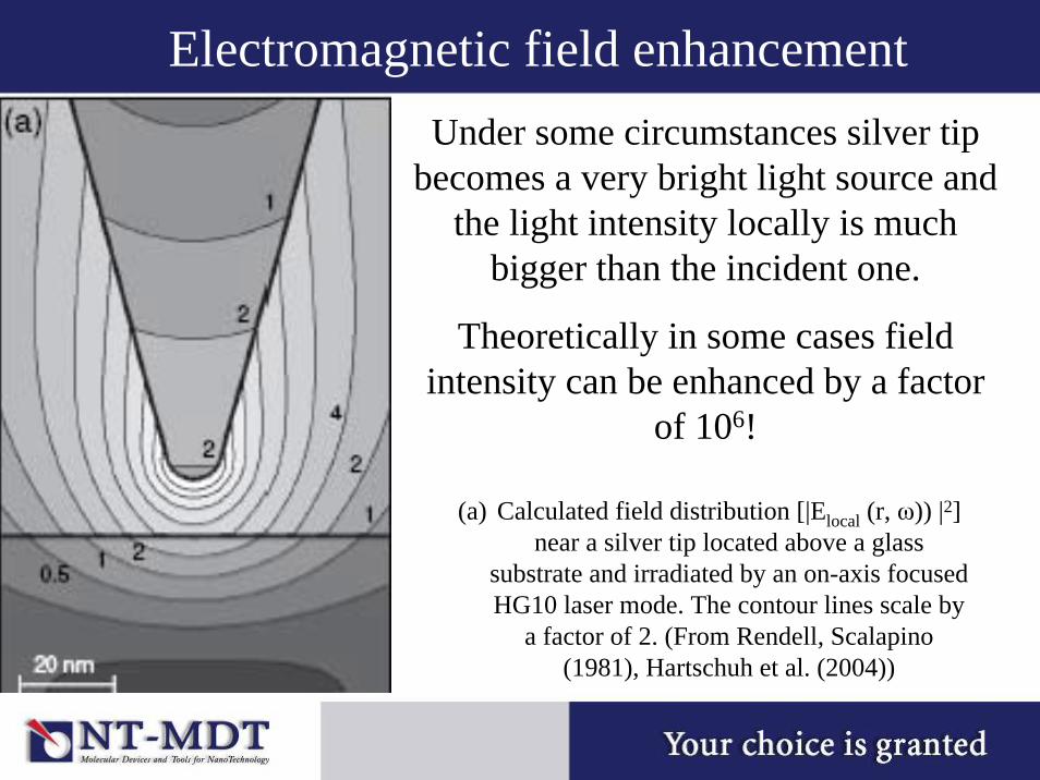
Electromagnetic field enhancement
(a) Calculated field distribution [|Elocal (r, ω)) |2] near a silver tip located above a glass
substrate and irradiated by an on-axis focused HG10 laser mode. The contour lines scale by
a factor of 2. (From Rendell, Scalapino(1981), Hartschuh et al. (2004))
Under some circumstances silver tip becomes a very bright light source and
the light intensity locally is much bigger than the incident one.
Theoretically in some cases field intensity can be enhanced by a factor
of 106!

Tip enhanced Raman set up
Tightly focused laser beam
Au or Ag coated glass
Sample
Au or Ag coated AFM tip
Zone of strong field enhancement
To the enhanced Raman signal detection system
Au or Ag coated tip placed 1-2 nm higher the sample surface (in semi-contact mode) provides strong Raman signal enhancement (today – by several orders of magnitude). Au or Ag glass coating serves for additional plasmon resonance enhancement. As the Raman signal from beneath the tip is much larger than neighboring far-field signals the whole system resolution is limited only by the zone of field enhancement which in turn depends on the tip shape and size. Point-by-point scanning gives full object image. Otherwise point localized spectroscopy is possible.
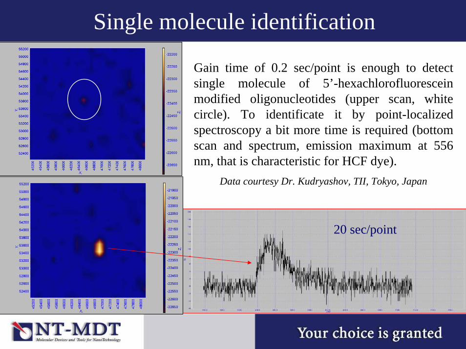
20 sec/point
Single molecule identification
Gain time of 0.2 sec/point is enough to detect single molecule of 5’-hexachlorofluorescein modified oligonucleotides (upper scan, white circle). To identificate it by point-localized spectroscopy a bit more time is required (bottom scan and spectrum, emission maximum at 556 nm, that is characteristic for HCF dye).
Data courtesy Dr. Kudryashov, TII, Tokyo, Japan

For more details on SERS see recent articles
Near-field Raman spectroscopy using a sharp metal tip. Journal of Microscopy, (2003), Vol. 210, pp. 234–240. Achim Hartschuh, N. Anderson, & LukasNovotny
Tip-enhanced optical spectroscopy (TEX Paper; Article submitted to RoyalSociety, 2004) Achim Hartschuh, Michael R. Beversluis, Alexandre Bouhelierand Lukas Novotny
High-Resolution Near-Field Raman Microscopy of Single-Walled CarbonNanotubes. PHYSICAL REVIEW LETTERS (2003) V.90, N.9. AchimHartschuh, Erik J. Sa´nchez, X. Sunney Xie, and Lukas Novotny
Near-field Raman scattering enhanced by a metallized tip. Chemical PhysicsLetters 335 (2001) 369-374. Norihiko Hayazawa et al.
Nanoscale chemical analysis by tip-enhanced Raman spectroscopy. Chemicalphysics letters 318 (2000) 131-136. Raoul M. Stockle et al.
Setup key features
NTEGRA spectra –
the instrument for scientific break-through
Spectrometer
Illumination system
Solutions for TERS
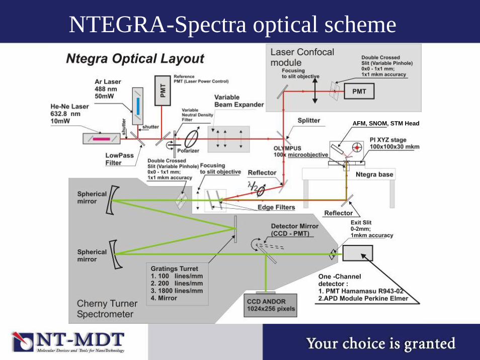
NTEGRA-Spectra optical scheme
AFM, SNOM, STM Head
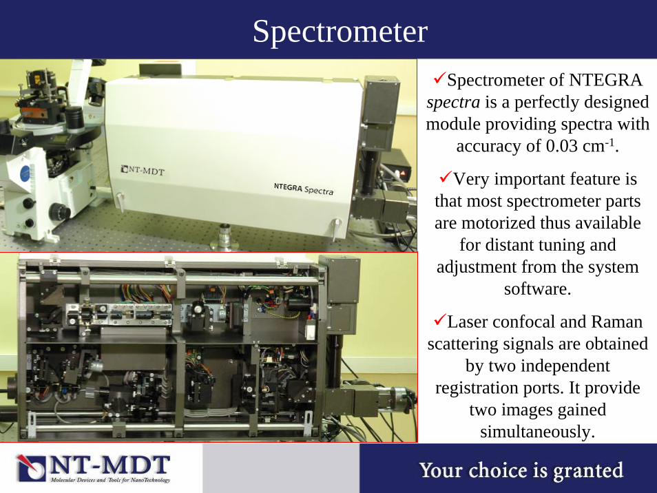
SpectrometerSpectrometer of NTEGRA
spectra is a perfectly designed module providing spectra with
accuracy of 0.03 cm-1.
Very important feature is that most spectrometer parts are motorized thus available
for distant tuning and adjustment from the system
software.
Laser confocal and Raman scattering signals are obtained
by two independent registration ports. It provide
two images gained simultaneously.
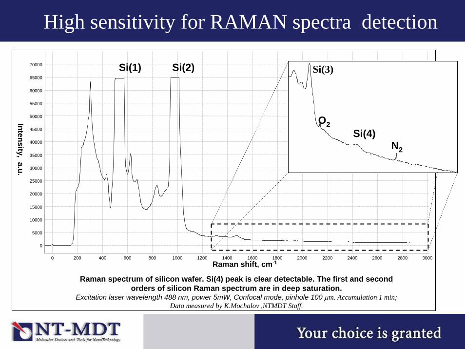
0
5000
10000
15000
20000
25000
30000
35000
40000
45000
50000
55000
60000
65000
70000
0 200 400 600 800 1000 1200 1400 1600 1800 2000 2200 2400 2600 2800 3000
Si(3)
O2
N2
Si(4)
Si(1) Si(2)
Raman shift, cm-1
Intensity, a.u.
Raman spectrum of silicon wafer. Si(4) peak is clear detectable. The first and second orders of silicon Raman spectrum are in deep saturation.
Excitation laser wavelength 488 nm, power 5mW, Confocal mode, pinhole 100 μm. Accumulation 1 min;Data measured by K.Mochalov ,NTMDT Staff.
High sensitivity for RAMAN spectra detection
How to choose a laserAs a whole Raman signal intensity is very low. About 1 photon of 107 incident ones is scattered by Raman effect.
I ~ 1/λ4
Raman signal intensity depends inversely on forth power of incident light wavelength. Laser with shorter wavelength gives stronger Raman signal. On the other hand it can be destructive
for some samples e.g. biological ones. Far-red light sources give very weak signal but it is fluorescence free and can penetrate
much deeper into the sample.
Thus it may be very helpful to change the light source during the experiment.
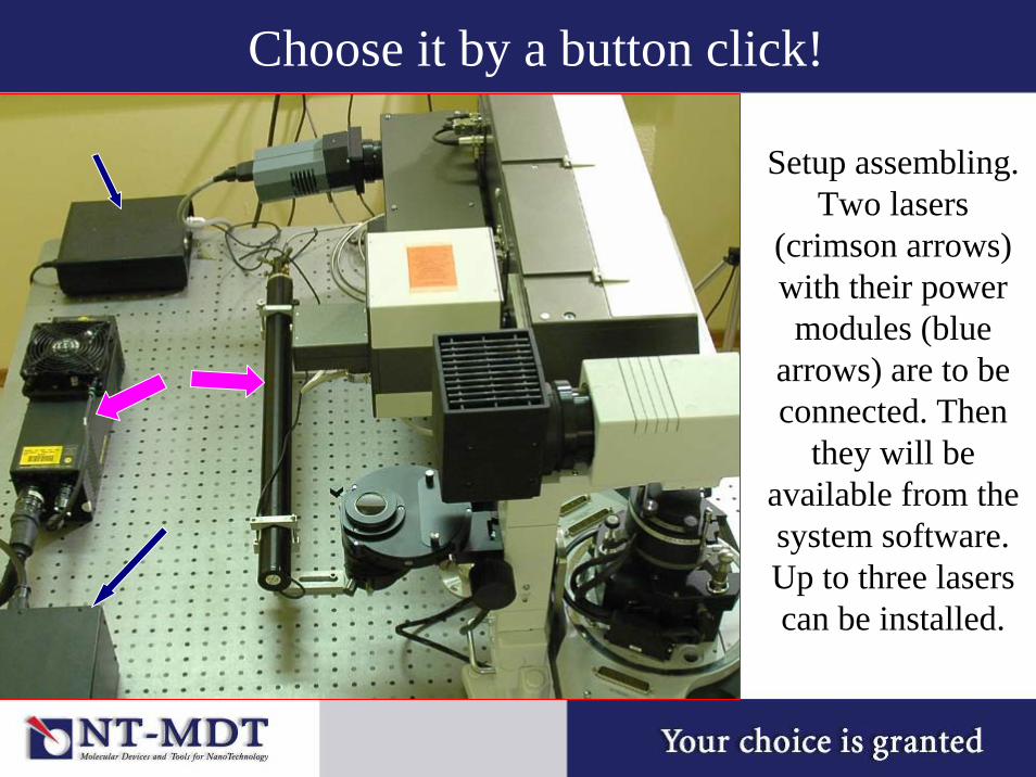
Choose it by a button click!
Setup assembling. Two lasers
(crimson arrows) with their power modules (blue
arrows) are to be connected. Then
they will be available from the system software. Up to three lasers can be installed.
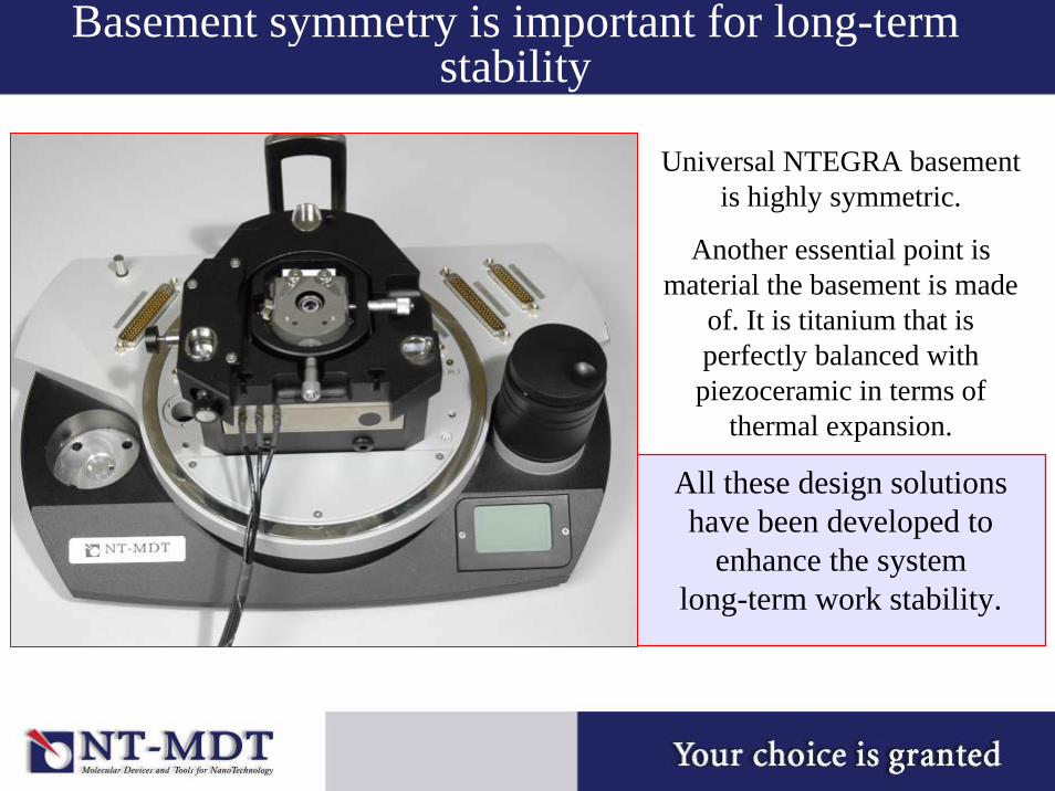
Basement symmetry is important for long-term stability
Universal NTEGRA basement is highly symmetric.
Another essential point is material the basement is made
of. It is titanium that is perfectly balanced with piezoceramic in terms of
thermal expansion.
All these design solutions have been developed to
enhance the system long-term work stability.
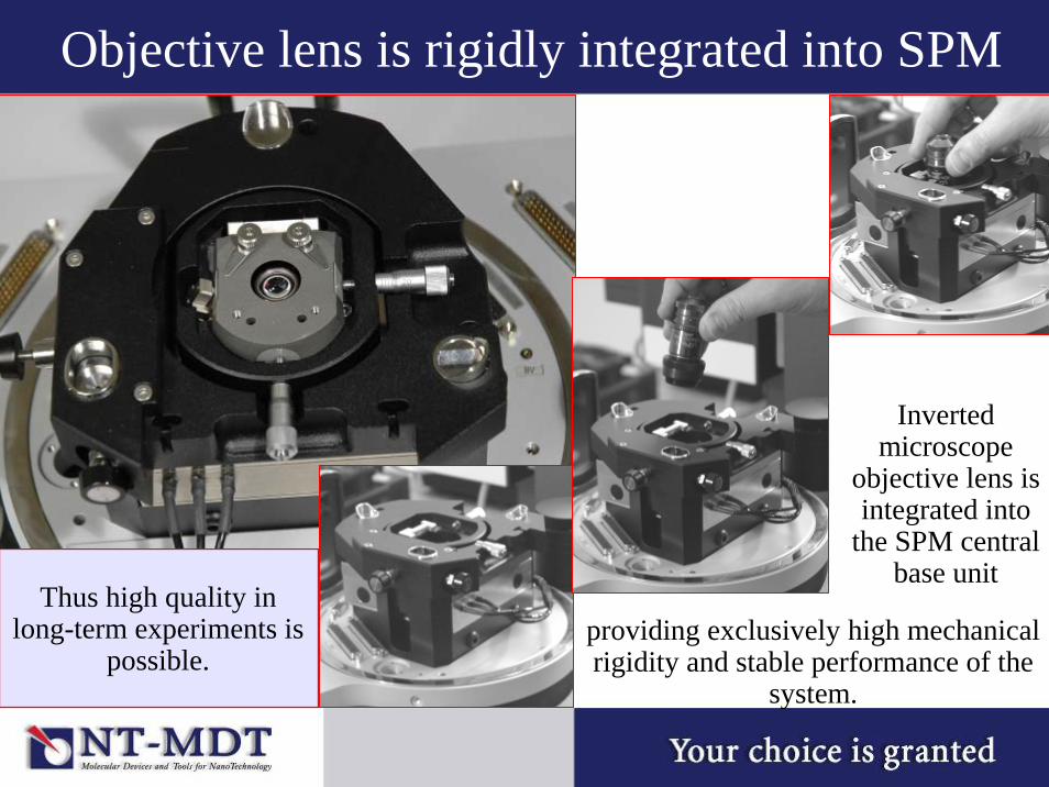
Objective lens is rigidly integrated into SPM
providing exclusively high mechanical rigidity and stable performance of the
system.
Inverted microscope
objective lens is integrated into
the SPM central base unit
Thus high quality in long-term experiments is
possible.
More solutions for TERS
High precision movement in Z direction (RMS≤5nm) makes it possible to perform TERS on filmsSpecial optical parts (TIR objectives, special polarizer
etc.) greatly increase the effectiveness of laser light conversion into surface plasmons thus increasing the TERS intensitySoftware tunable pinhole provides optimal choice
between resolution and sensitivityTransparent objects can be studied with inverted microscope
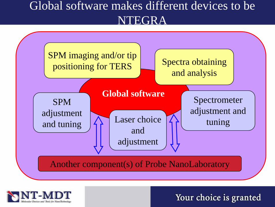
Global software makes different devices to be NTEGRA
Spectrometer adjustment and
tuning
Global software
Spectra obtaining and analysis
Laser choice and
adjustment
SPM adjustment and tuning
SPM imaging and/or tip positioning for TERS
Another component(s) of Probe NanoLaboratory

Applications:
Real experiments prove the performance
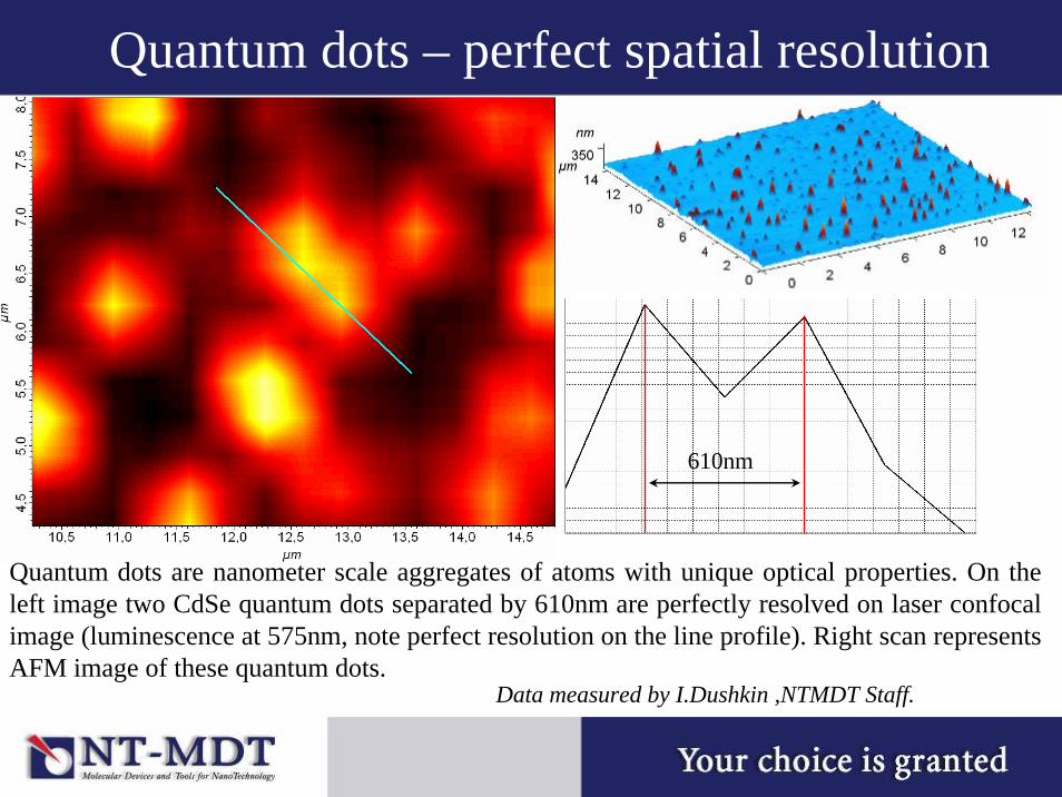
Quantum dots – perfect spatial resolution
Quantum dots are nanometer scale aggregates of atoms with unique optical properties. On the left image two CdSe quantum dots separated by 610nm are perfectly resolved on laser confocalimage (luminescence at 575nm, note perfect resolution on the line profile). Right scan represents AFM image of these quantum dots.
610nm
Data measured by I.Dushkin ,NTMDT Staff.
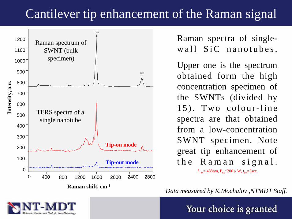
Cantilever tip enhancement of the Raman signalIn
tens
ity, a
.u.
0
100
200
300
400
500
600
700
800
900
1000
1100
1200
0 400 800 1200 1600 2000 2400 2800
Raman shift, cm-1
Raman spectrum of SWNT (bulk
specimen)
Tip-on mode
1595
TERS spectra of a single nanotube
2697
Tip-out mode
Raman spectra of single-w a l l S i C n a n o t u b e s .
Upper one is the spectrum obtained form the high concentration specimen of the SWNTs (divided by 15 ) . Two co lou r - l i ne spectra are that obtained from a low-concentration SWNT specimen. Note great tip enhancement of t h e R a m a n s i g n a l .
λex= 488nm, Pex~200μW, tint=5sec.
Data measured by K.Mochalov ,NTMDT Staff.
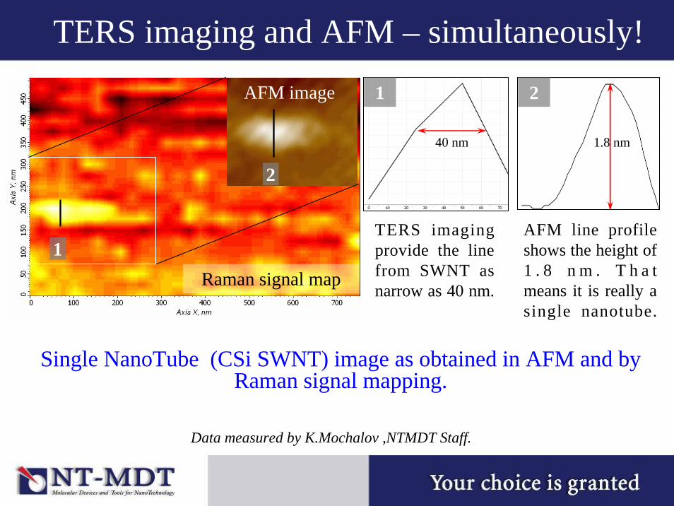
TERS imaging and AFM – simultaneously!
AFM image
Raman signal map1
2
1 2
40 nm 1.8 nm
Single NanoTube (CSi SWNT) image as obtained in AFM and by Raman signal mapping.
TERS imaging provide the line from SWNT as narrow as 40 nm.
AFM line profile shows the height of 1 . 8 n m . T h a t means it is really a single nanotube.
Data measured by K.Mochalov ,NTMDT Staff.
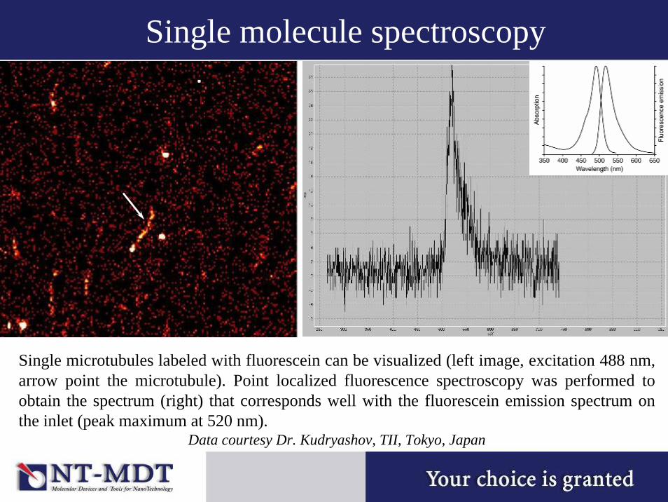
Single molecule spectroscopy
Single microtubules labeled with fluorescein can be visualized (left image, excitation 488 nm, arrow point the microtubule). Point localized fluorescence spectroscopy was performed to obtain the spectrum (right) that corresponds well with the fluorescein emission spectrum on the inlet (peak maximum at 520 nm).
Data courtesy Dr. Kudryashov, TII, Tokyo, Japan
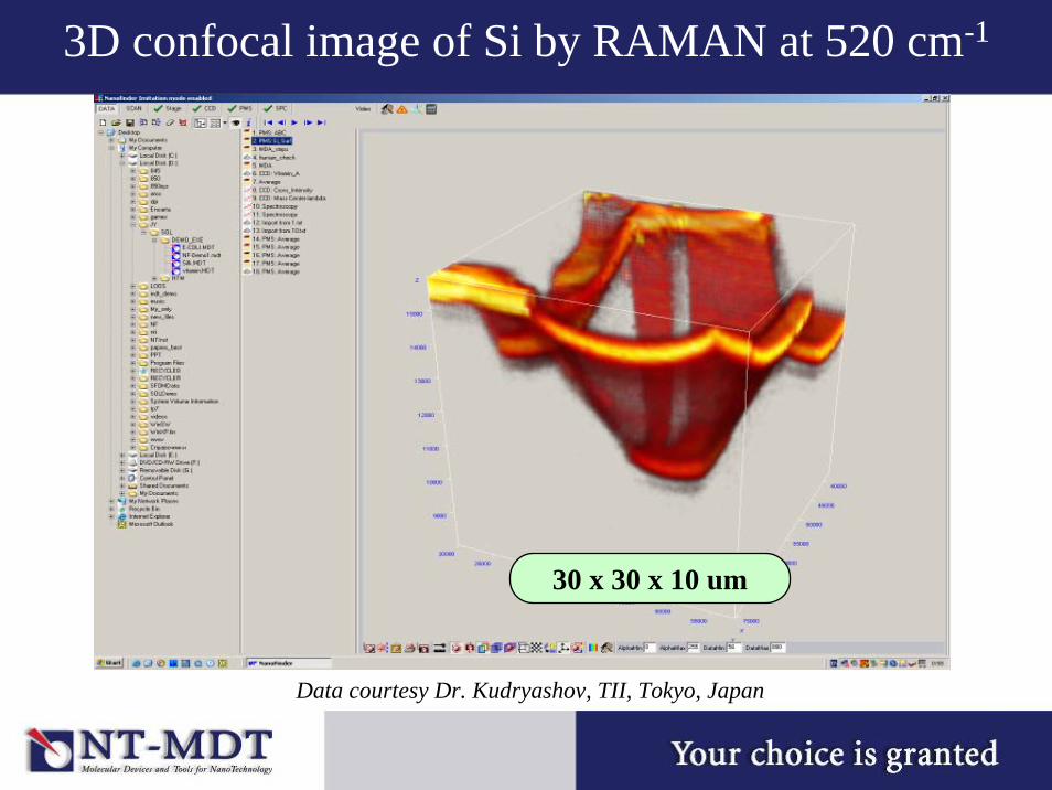
30 x 30 x 10 um
Data courtesy Dr. Kudryashov, TII, Tokyo, Japan
3D confocal image of Si by RAMAN at 520 cm-1
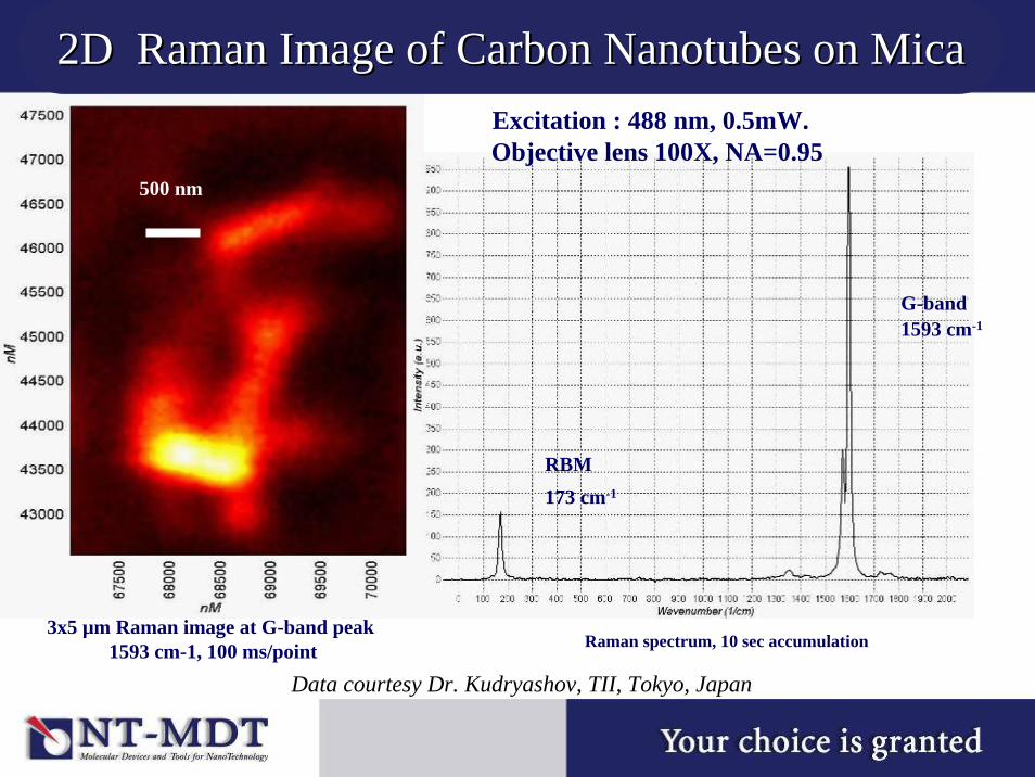
500 nm
1593 cm-1
173 cm-1
RBM
G-band
3x5 µm Raman image at G-band peak 1593 cm-1, 100 ms/point Raman spectrum, 10 sec accumulation
Excitation : 488 nm, 0.5mW. Objective lens 100X, NA=0.95
2D Raman Image of Carbon 2D Raman Image of Carbon NanotubesNanotubes on Micaon Mica
Data courtesy Dr. Kudryashov, TII, Tokyo, Japan
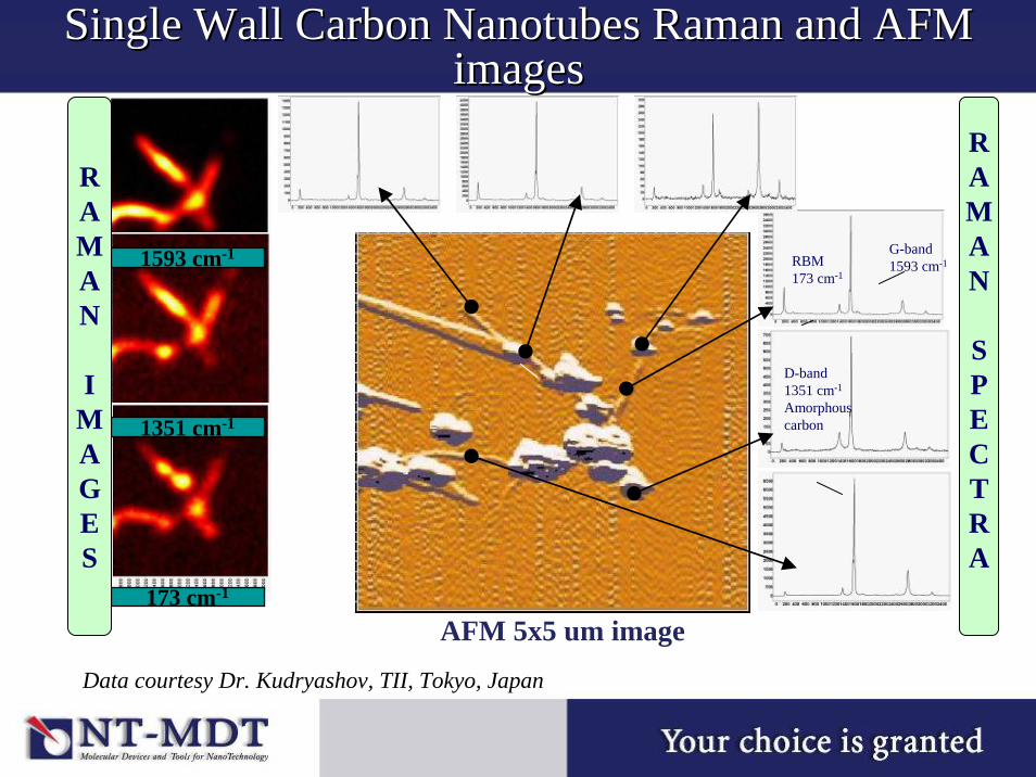
AFM 5x5 um image
Single Wall Carbon Single Wall Carbon NanotubesNanotubes Raman and AFM Raman and AFM imagesimages
RBM173 cm-1
G-band1593 cm-1
D-band1351 cm-1
Amorphouscarbon
1593 cm-1
1351 cm-1
173 cm-1
RAMAN
IMAGES
RAMAN
SPECTRA
Data courtesy Dr. Kudryashov, TII, Tokyo, Japan