
Transient Suppression Techniques - AC-DC Converters c5 47µf d2 ug8bt r2 68 Ω r6 270 Ω to 620 ...
8
June 1996 Introduction AC power mains occasionally have transient surge voltages. Lightning strikes and AC mains load switching are just two examples of many possible conditions causing transient voltages. Consequently, all off-line power supplies must provide some level of protection to suppress the effects of such transient voltages. This application note presents design techniques which improve TOPSwitch power supply operation through most AC mains transient surge voltages. Properly designed transformers, PC boards, and EMI filters not only suppress the effects from transient voltages but also reduce both conducted and radiated EMI emissions as well. These techniques can also be used in applications with DC input voltages such as Telecom and Television Cable Communication (or Cablecom). The ST202A Reference Design Board using the TOP202YAI TOPSwitch will be used as an example throughout this application note. Refer to the ST202A data sheet as well as AN-14 and AN-15 for additional information. Typical Transient Test Voltages Figure 1 shows a typical surge voltage waveform specified by IEC 1000-4-5 (formerly IEC 801-4-5). Peak test voltages (U) of 3kV are common but in some applications higher peak voltages are specified. The surge voltage waveform has a 1.2μS front time T 1 and 50μS time to half value T 2 as shown. Figure 2 shows a typical ring wave voltage waveform specified by IEEE-587. Peak test voltages (V peak ) of 3kV are common but in some applications higher voltages are specified. The open circuit ring wave voltage waveform has a 0.5μS rise time to 90% of peak value and exponentially decays while oscillating at 100 kHz with each peak being 60% of the preceding peak. The transient test voltage may be applied both in common mode and differential mode configurations. The common mode configuration shown in Figure 3 applies the transient test voltage first to one AC mains conductor and then the other with respect to earth ground. The TOPSwitch power supply output should be connected either directly to earth ground or AC coupled through a capacitor to earth ground. This transient test voltage causes high peak transient ringing currents to flow between the TOPSwitch power supply primary and secondary. Without proper attention to EMI filter design, transformer design, and PC layout design, transient currents couple into signal traces and generate voltage spikes capable of setting the TOPSwitch shutdown latch. U T t T 1 T 2 1.0 0.9 0.5 0.3 0.1 0.0 PI-1709-120595 Front Time T 1 = 1.67 x T = 1.2 μs ± 30% Time To Half Value T 2 = 50 μs ± 20% Figure 1. Waveshape of Open Circuit Voltage (1.2/50 μS) From IEC-1000-4-5. 0.9 V peak 60% OF V peak 0.1 V peak 0.5 μs T = 10 μs (f = 100 kHz) V peak PI-1710-120595 Figure 2. 0.5 μs-100 kHz Ring Wave (Open-Circuit Voltage) From IEEE-587. ® Transient Suppression Techniques for TOPSwitch ® Power Supplies Application Note AN-20
Transcript of Transient Suppression Techniques - AC-DC Converters c5 47µf d2 ug8bt r2 68 Ω r6 270 Ω to 620 ...
June 1996
IntroductionAC power mains occasionally have transient surge voltages.Lightning strikes and AC mains load switching are just twoexamples of many possible conditions causing transient voltages.Consequently, all off-line power supplies must provide somelevel of protection to suppress the effects of such transientvoltages.
This application note presents design techniques which improveTOPSwitch power supply operation through most AC mainstransient surge voltages. Properly designed transformers, PCboards, and EMI filters not only suppress the effects fromtransient voltages but also reduce both conducted and radiatedEMI emissions as well. These techniques can also be used inapplications with DC input voltages such as Telecom andTelevision Cable Communication (or Cablecom).
The ST202A Reference Design Board using the TOP202YAITOPSwitch will be used as an example throughout thisapplication note. Refer to the ST202A data sheet as well asAN-14 and AN-15 for additional information.
Typical Transient Test Voltages
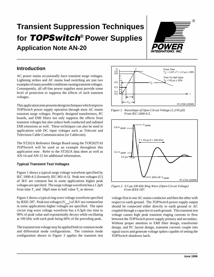
Figure 1 shows a typical surge voltage waveform specified byIEC 1000-4-5 (formerly IEC 801-4-5). Peak test voltages (U)of 3kV are common but in some applications higher peakvoltages are specified. The surge voltage waveform has a 1.2µSfront time T
1 and 50µS time to half value T
2 as shown.
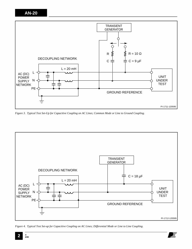
Figure 2 shows a typical ring wave voltage waveform specifiedby IEEE-587. Peak test voltages (V
peak) of 3kV are common but
in some applications higher voltages are specified. The opencircuit ring wave voltage waveform has a 0.5µS rise time to90% of peak value and exponentially decays while oscillatingat 100 kHz with each peak being 60% of the preceding peak.
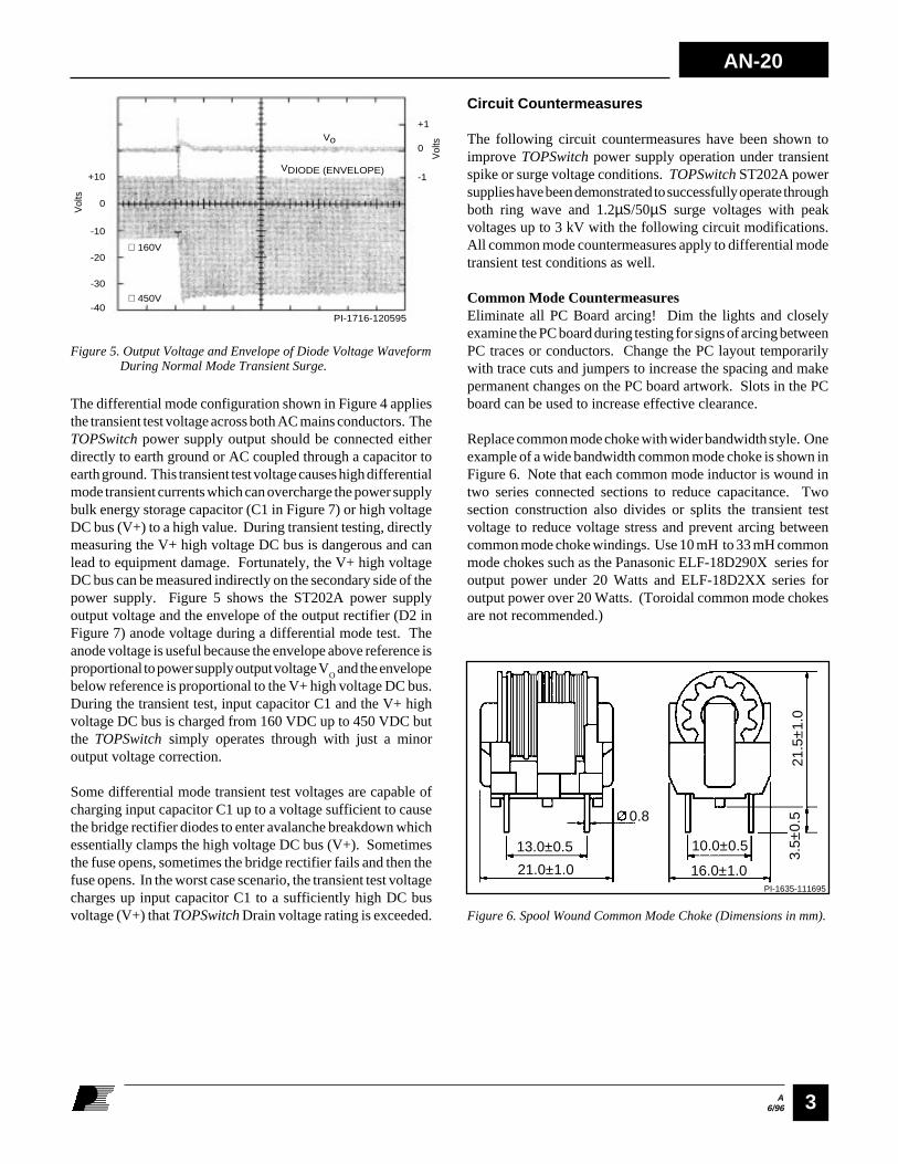
The transient test voltage may be applied both in common modeand differential mode configurations. The common modeconfiguration shown in Figure 3 applies the transient test
voltage first to one AC mains conductor and then the other withrespect to earth ground. The TOPSwitch power supply outputshould be connected either directly to earth ground or ACcoupled through a capacitor to earth ground. This transient testvoltage causes high peak transient ringing currents to flowbetween the TOPSwitch power supply primary and secondary.Without proper attention to EMI filter design, transformerdesign, and PC layout design, transient currents couple intosignal traces and generate voltage spikes capable of setting theTOPSwitch shutdown latch.
U
Tt
T1
T2
1.00.9
0.5
0.3
0.10.0
PI-1709-120595
Front Time T1 = 1.67 x T = 1.2 µs ± 30% Time To Half Value T2 = 50 µs ± 20%
Figure 1. Waveshape of Open Circuit Voltage (1.2/50 µS) From IEC-1000-4-5.
0.9 V peak
60% OF V peak
0.1 V peak
0.5 µs
T = 10 µs (f = 100 kHz)
V peak
PI-1710-120595
Figure 2. 0.5 µs-100 kHz Ring Wave (Open-Circuit Voltage)From IEEE-587.
®
Transient Suppression Techniques
for TOPSwitch® Power SuppliesApplication Note AN-20
AN-20
A6/962
TRANSIENTGENERATOR
DECOUPLING NETWORK
AC (DC)POWERSUPPLY
NETWORK
L
R
C
R = 10 Ω
C = 9 µF
L = 20 mH
N
PEGROUND REFERENCE
UNITUNDER
TEST
PI-1711-120595
Figure 3. Typical Test Set-Up for Capacitive Coupling on AC Lines; Common Mode or Line to Ground Coupling.
Figure 4. Typical Test Set-up for Capacitive Coupling on AC Lines; Differential Mode or Line to Line Coupling.
TRANSIENTGENERATOR
DECOUPLING NETWORK
AC (DC)POWERSUPPLY
NETWORK
L
C = 18 µFL = 20 mH
N
PEGROUND REFERENCE
PI-1712-120595
UNITUNDER
TEST
A6/96
AN-20
3
+1
-1
0
0
-10
+10
Vol
ts
Vol
ts
∝160V
∝450V
-20
-30
-40PI-1716-120595
Vo
VDIODE (ENVELOPE)
Figure 5. Output Voltage and Envelope of Diode Voltage Waveform During Normal Mode Transient Surge.
Circuit Countermeasures
The following circuit countermeasures have been shown toimprove TOPSwitch power supply operation under transientspike or surge voltage conditions. TOPSwitch ST202A powersupplies have been demonstrated to successfully operate throughboth ring wave and 1.2µS/50µS surge voltages with peakvoltages up to 3 kV with the following circuit modifications.All common mode countermeasures apply to differential modetransient test conditions as well.
Common Mode CountermeasuresEliminate all PC Board arcing! Dim the lights and closelyexamine the PC board during testing for signs of arcing betweenPC traces or conductors. Change the PC layout temporarilywith trace cuts and jumpers to increase the spacing and makepermanent changes on the PC board artwork. Slots in the PCboard can be used to increase effective clearance.
Replace common mode choke with wider bandwidth style. Oneexample of a wide bandwidth common mode choke is shown inFigure 6. Note that each common mode inductor is wound intwo series connected sections to reduce capacitance. Twosection construction also divides or splits the transient testvoltage to reduce voltage stress and prevent arcing betweencommon mode choke windings. Use 10 mH to 33 mH commonmode chokes such as the Panasonic ELF-18D290X series foroutput power under 20 Watts and ELF-18D2XX series foroutput power over 20 Watts. (Toroidal common mode chokesare not recommended.)
The differential mode configuration shown in Figure 4 appliesthe transient test voltage across both AC mains conductors. TheTOPSwitch power supply output should be connected eitherdirectly to earth ground or AC coupled through a capacitor toearth ground. This transient test voltage causes high differentialmode transient currents which can overcharge the power supplybulk energy storage capacitor (C1 in Figure 7) or high voltageDC bus (V+) to a high value. During transient testing, directlymeasuring the V+ high voltage DC bus is dangerous and canlead to equipment damage. Fortunately, the V+ high voltageDC bus can be measured indirectly on the secondary side of thepower supply. Figure 5 shows the ST202A power supplyoutput voltage and the envelope of the output rectifier (D2 inFigure 7) anode voltage during a differential mode test. Theanode voltage is useful because the envelope above reference isproportional to power supply output voltage V
O and the envelope
below reference is proportional to the V+ high voltage DC bus.During the transient test, input capacitor C1 and the V+ highvoltage DC bus is charged from 160 VDC up to 450 VDC butthe TOPSwitch simply operates through with just a minoroutput voltage correction.
Some differential mode transient test voltages are capable ofcharging input capacitor C1 up to a voltage sufficient to causethe bridge rectifier diodes to enter avalanche breakdown whichessentially clamps the high voltage DC bus (V+). Sometimesthe fuse opens, sometimes the bridge rectifier fails and then thefuse opens. In the worst case scenario, the transient test voltagecharges up input capacitor C1 to a sufficiently high DC busvoltage (V+) that TOPSwitch Drain voltage rating is exceeded.
0.8
13.0±0.5
21.0±1.0
10.0±0.5
16.0±1.0
21.5
±1.
03.
5±0.
5
PI-1635-111695
Figure 6. Spool Wound Common Mode Choke (Dimensions in mm).
AN-20
A6/964
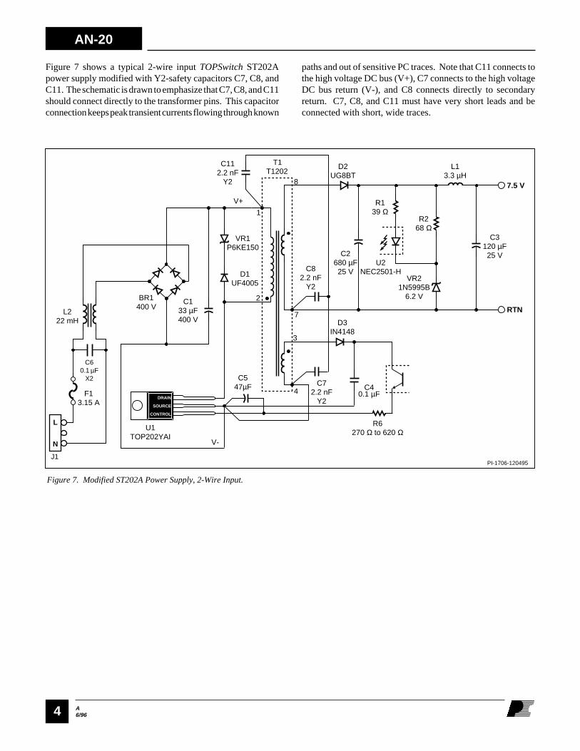
Figure 7 shows a typical 2-wire input TOPSwitch ST202Apower supply modified with Y2-safety capacitors C7, C8, andC11. The schematic is drawn to emphasize that C7, C8, and C11should connect directly to the transformer pins. This capacitorconnection keeps peak transient currents flowing through known
paths and out of sensitive PC traces. Note that C11 connects tothe high voltage DC bus (V+), C7 connects to the high voltageDC bus return (V-), and C8 connects directly to secondaryreturn. C7, C8, and C11 must have very short leads and beconnected with short, wide traces.
PI-1706-120495
7.5 V
RTN
C547µF
D2UG8BT
R268 Ω
R6270 Ω to 620 Ω
VR21N5995B
6.2 V
C3120 µF25 V
T1
D1UF4005
C2680 µF25 V
VR1P6KE150
BR1400 V
C133 µF400 V
C112.2 nF
Y2
R139 Ω
U2NEC2501-H
U1TOP202YAI
DRAIN
SOURCE
CONTROL
C40.1 µF
L13.3 µH
F13.15 A
J1
C60.1 µF
X2
L222 mH
L
N
T1202
1
8
2
7
3
4
C82.2 nF
Y2
C72.2 nF
Y2
D3IN4148
V+
V-
Figure 7. Modified ST202A Power Supply, 2-Wire Input.
A6/96
AN-20
5
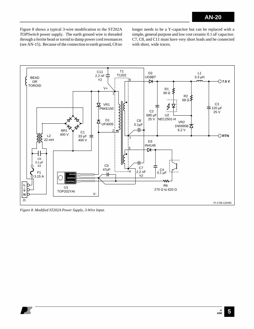
Figure 8. Modified ST202A Power Supply, 3-Wire Input.
Figure 8 shows a typical 3-wire modification to the ST202ATOPSwitch power supply. The earth ground wire is threadedthrough a ferrite bead or toroid to damp power cord resonances(see AN-15). Because of the connection to earth ground, C8 no
longer needs to be a Y-capacitor but can be replaced with asimple, general purpose and low cost ceramic 0.1 uF capacitor.C7, C8, and C11 must have very short leads and be connectedwith short, wide traces.
PI-1708-120495
7.5 V
RTN
C547µF
D2UG8BT
R268 Ω
R6270 Ω to 620 Ω
VR21N5995B
6.2 V
C3120 µF25 V
T1
D1UF4005
C2680 µF25 V
VR1P6KE150
BR1400 V
C133 µF400 V
C112.2 nF
Y2
R139 Ω
U2NEC2501-H
U1TOP202YAI
DRAIN
SOURCE
CONTROL
C40.1 µF
L13.3 µH
F13.15 A
J1
C60.1 µF
X2
L222 mH
L
N
T1202
1
8
2
7
3
4
C80.1µF
C72.2 nF
Y2
D3IN4148
BEADOR
TOROIDV+
V-
AN-20
A6/966
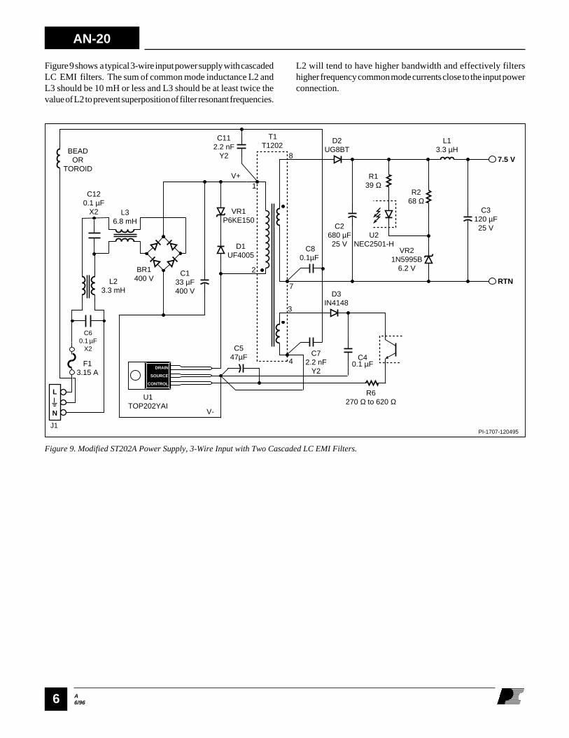
Figure 9 shows a typical 3-wire input power supply with cascadedLC EMI filters. The sum of common mode inductance L2 andL3 should be 10 mH or less and L3 should be at least twice thevalue of L2 to prevent superposition of filter resonant frequencies.
L2 will tend to have higher bandwidth and effectively filtershigher frequency common mode currents close to the input powerconnection.
PI-1707-120495
7.5 V
RTN
C547µF
D2UG8BT
R268 Ω
R6270 Ω to 620 Ω
VR21N5995B
6.2 V
C3120 µF25 V
T1
D1UF4005
C2680 µF25 V
VR1P6KE150
BR1400 V
C133 µF400 V
C120.1 µF
X2
C112.2 nF
Y2
R139 Ω
U2NEC2501-H
U1TOP202YAI
DRAIN
SOURCE
CONTROL
C40.1 µF
L13.3 µH
F13.15 A
J1
C60.1 µF
X2
L23.3 mH
L36.8 mH
L
N
T1202
1
8
2
7
3
4
C80.1µF
C72.2 nF
Y2
D3IN4148
BEADOR
TOROIDV+
V-
Figure 9. Modified ST202A Power Supply, 3-Wire Input with Two Cascaded LC EMI Filters.
A6/96
AN-20
7
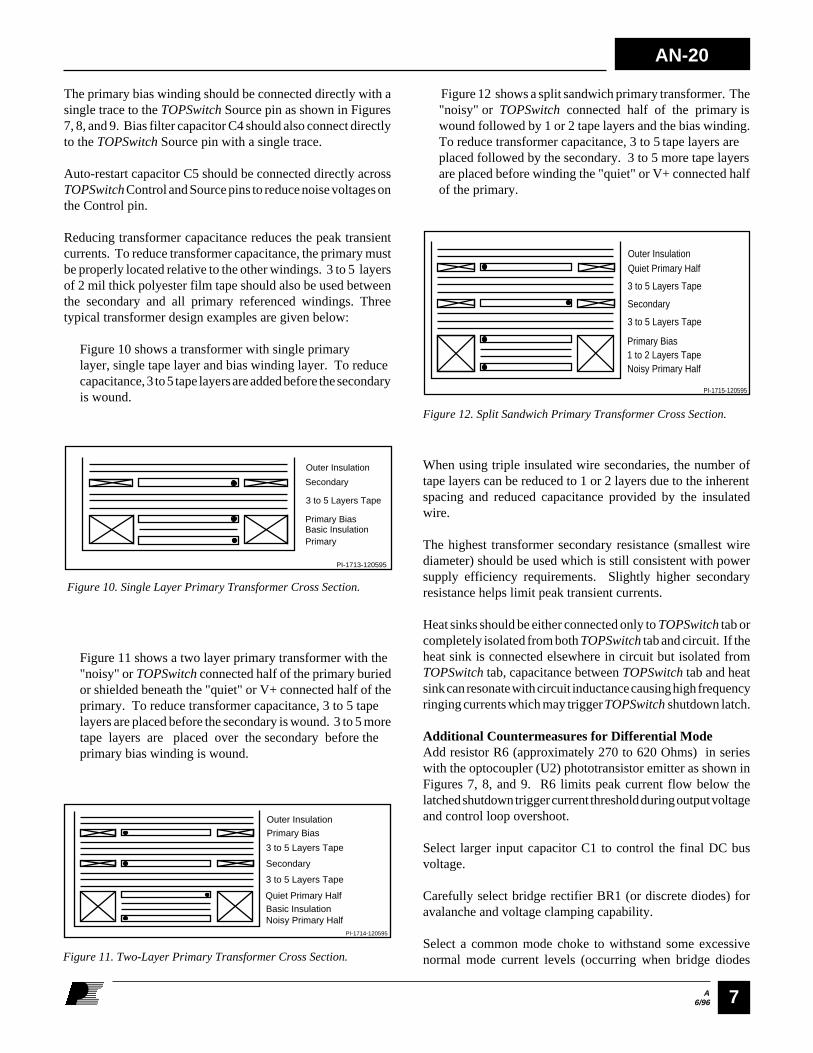
Figure 12 shows a split sandwich primary transformer. The"noisy" or TOPSwitch connected half of the primary iswound followed by 1 or 2 tape layers and the bias winding.To reduce transformer capacitance, 3 to 5 tape layers areplaced followed by the secondary. 3 to 5 more tape layersare placed before winding the "quiet" or V+ connected halfof the primary.
The primary bias winding should be connected directly with asingle trace to the TOPSwitch Source pin as shown in Figures7, 8, and 9. Bias filter capacitor C4 should also connect directlyto the TOPSwitch Source pin with a single trace.
Auto-restart capacitor C5 should be connected directly acrossTOPSwitch Control and Source pins to reduce noise voltages onthe Control pin.
Reducing transformer capacitance reduces the peak transientcurrents. To reduce transformer capacitance, the primary mustbe properly located relative to the other windings. 3 to 5 layersof 2 mil thick polyester film tape should also be used betweenthe secondary and all primary referenced windings. Threetypical transformer design examples are given below:
Figure 10 shows a transformer with single primarylayer, single tape layer and bias winding layer. To reducecapacitance, 3 to 5 tape layers are added before the secondaryis wound.
Figure 11. Two-Layer Primary Transformer Cross Section.
PI-1714-120595
Outer Insulation
Primary Bias
3 to 5 Layers Tape
Secondary
3 to 5 Layers Tape
Quiet Primary HalfBasic InsulationNoisy Primary Half
Figure 11 shows a two layer primary transformer with the"noisy" or TOPSwitch connected half of the primary buriedor shielded beneath the "quiet" or V+ connected half of theprimary. To reduce transformer capacitance, 3 to 5 tapelayers are placed before the secondary is wound. 3 to 5 moretape layers are placed over the secondary before theprimary bias winding is wound.
PI-1715-120595
Outer InsulationQuiet Primary Half
3 to 5 Layers Tape
Secondary
3 to 5 Layers Tape
Primary Bias1 to 2 Layers TapeNoisy Primary Half
Figure 12. Split Sandwich Primary Transformer Cross Section.
When using triple insulated wire secondaries, the number oftape layers can be reduced to 1 or 2 layers due to the inherentspacing and reduced capacitance provided by the insulatedwire.
The highest transformer secondary resistance (smallest wirediameter) should be used which is still consistent with powersupply efficiency requirements. Slightly higher secondaryresistance helps limit peak transient currents.
Heat sinks should be either connected only to TOPSwitch tab orcompletely isolated from both TOPSwitch tab and circuit. If theheat sink is connected elsewhere in circuit but isolated fromTOPSwitch tab, capacitance between TOPSwitch tab and heatsink can resonate with circuit inductance causing high frequencyringing currents which may trigger TOPSwitch shutdown latch.
Additional Countermeasures for Differential ModeAdd resistor R6 (approximately 270 to 620 Ohms) in serieswith the optocoupler (U2) phototransistor emitter as shown inFigures 7, 8, and 9. R6 limits peak current flow below thelatched shutdown trigger current threshold during output voltageand control loop overshoot.
Select larger input capacitor C1 to control the final DC busvoltage.
Carefully select bridge rectifier BR1 (or discrete diodes) foravalanche and voltage clamping capability.
Select a common mode choke to withstand some excessivenormal mode current levels (occurring when bridge diodes
PI-1713-120595
Outer Insulation
3 to 5 Layers Tape
Primary Bias
PrimaryBasic Insulation
Secondary
Figure 10. Single Layer Primary Transformer Cross Section.
AN-20
A6/968
PI-1717-120595
F1L2
BR1
V+
V-
TO POWER SUPPLY
C60.1 µF
X2
VR3MOV
COMMONMODE
CHOKE
L
N
Figure 13. MOV VR3 Position Relative to X-Capacitor C6, Common Mode Choke L2 and Bridge Rectifier BR1.
avalanche and clamp the V+ high voltage DC bus) withoutcausing sufficient coil magnetostriction to stress and crack theferrite core.
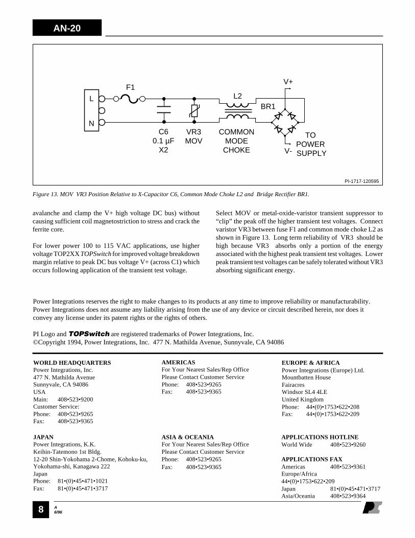
For lower power 100 to 115 VAC applications, use highervoltage TOP2XX TOPSwitch for improved voltage breakdownmargin relative to peak DC bus voltage V+ (across C1) whichoccurs following application of the transient test voltage.
Select MOV or metal-oxide-varistor transient suppressor to“clip” the peak off the higher transient test voltages. Connectvaristor VR3 between fuse F1 and common mode choke L2 asshown in Figure 13. Long term reliability of VR3 should behigh because VR3 absorbs only a portion of the energyassociated with the highest peak transient test voltages. Lowerpeak transient test voltages can be safely tolerated without VR3absorbing significant energy.
JAPANPower Integrations, K.K.Keihin-Tatemono 1st Bldg.12-20 Shin-Yokohama 2-Chome, Kohoku-ku,Yokohama-shi, Kanagawa 222JapanPhone: 81•(0)•45•471•1021Fax: 81•(0)•45•471•3717
ASIA & OCEANIAFor Your Nearest Sales/Rep OfficePlease Contact Customer ServicePhone: 408•523•9265Fax: 408•523•9365
WORLD HEADQUARTERSPower Integrations, Inc.477 N. Mathilda AvenueSunnyvale, CA 94086USAMain: 408•523•9200Customer Service:Phone: 408•523•9265Fax: 408•523•9365
AMERICASFor Your Nearest Sales/Rep OfficePlease Contact Customer ServicePhone: 408•523•9265Fax: 408•523•9365
Power Integrations reserves the right to make changes to its products at any time to improve reliability or manufacturability.Power Integrations does not assume any liability arising from the use of any device or circuit described herein, nor does itconvey any license under its patent rights or the rights of others.
PI Logo and TOPSwitch are registered trademarks of Power Integrations, Inc.©Copyright 1994, Power Integrations, Inc. 477 N. Mathilda Avenue, Sunnyvale, CA 94086
APPLICATIONS HOTLINEWorld Wide 408•523•9260
APPLICATIONS FAXAmericas 408•523•9361Europe/Africa44•(0)•1753•622•209Japan 81•(0)•45•471•3717Asia/Oceania 408•523•9364
EUROPE & AFRICAPower Integrations (Europe) Ltd.Mountbatten HouseFairacresWindsor SL4 4LEUnited KingdomPhone: 44•(0)•1753•622•208Fax: 44•(0)•1753•622•209


![LABORATÓRIO DE SISTEMAS MECATRÔNICOS E ROBÓTICA ] - LAB.pdf · Resistores - 1,0 Ω - 100k Ω 1,2 Ω - 120k Ω 1,5 Ω - 150k Ω 1,8 Ω- 180k Ω 2,2 Ω– 220k Ω 2,7 Ω– 270k](https://static.fdocument.org/doc/165x107/5c245c1a09d3f224508c4b48/laboratorio-de-sistemas-mecatronicos-e-robotica-labpdf-resistores-.jpg)