TPS60151 5-V and 140-mA Charge Pump datasheet (Rev. A) · 90 100 Efficiency - % 10 mA 50 mA 150 mA...
27
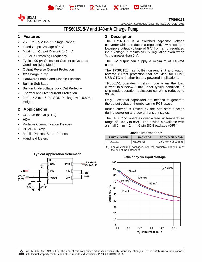
2.7 3.2 3.7 4.2 4.7 5.2 V - Input Voltage - V I 0 10 20 30 40 50 60 70 80 90 100 Efficiency - % 10 mA 50 mA 150 mA 120 mA 100 mA T = 25°C A C1 4.7μF CP- VIN VOUT GND CP+ ENA C3 2.2μF C2 2.2μF VIN VOUT (5.0V) ENABLE /DISABLE Product Folder Sample & Buy Technical Documents Tools & Software Support & Community TPS60151 SLVSA02A – SEPTEMBER 2009 – REVISED OCTOBER 2015 TPS60151 5-V and 140-mA Charge Pump 1 Features 3 Description The TPS60151 is a switched capacitor voltage 1• 2.7 V to 5.5 V Input Voltage Range converter which produces a regulated, low noise, and • Fixed Output Voltage of 5 V low-ripple output voltage of 5 V from an unregulated • Maximum Output Current: 140 mA input voltage. It maintains 5-V regulation even when V IN is greater than 5 V. • 1.5 MHz Switching Frequency • Typical 90-μA Quiescent Current at No Load The 5-V output can supply a minimum of 140-mA Condition (Skip Mode) current. • Output Reverse Current Protection The TPS60151 has built-in current limit and output reverse current protection that are ideal for HDMI, • X2 Charge Pump USB OTG and other battery powered applications. • Hardware Enable and Disable Function TPS60151 operates in skip mode when the load • Built-in Soft Start current falls below 8 mA under typical condition. In • Built-in Undervoltage Lock Out Protection skip mode operation, quiescent current is reduced to • Thermal and Over-current Protection 90 μA. • 2-mm × 2-mm 6-Pin SON-Package with 0.8-mm Only 3 external capacitors are needed to generate Height the output voltage, thereby saving PCB space. Inrush current is limited by the soft start function 2 Applications during power on and power transient states. • USB On the Go (OTG) The TPS60151 operates over a free air temperature • HDMI range of –40°C to 85°C. The device is available with • Portable Communication Devices a small 2-mm × 2-mm 6-pin SON package (QFN). • PCMCIA Cards Device Information (1) • Mobile Phones, Smart Phones PART NUMBER PACKAGE BODY SIZE (NOM) • Handheld Meters TPS60151 WSON (6) 2.00 mm × 2.00 mm (1) For all available packages, see the orderable addendum at the end of the datasheet. Typical Application Schematic Efficiency vs Input Voltage 1 An IMPORTANT NOTICE at the end of this data sheet addresses availability, warranty, changes, use in safety-critical applications, intellectual property matters and other important disclaimers. PRODUCTION DATA.
Transcript of TPS60151 5-V and 140-mA Charge Pump datasheet (Rev. A) · 90 100 Efficiency - % 10 mA 50 mA 150 mA...
2.7 3.2 3.7 4.2 4.7 5.2
V - Input Voltage - VI
0
10
20
30
40
50
60
70
80
90
100
Eff
icie
ncy -
%
10 mA
50 mA
150 mA
120 mA
100 mA
T = 25°CA
C14.7μF
CP-VIN
VOUT
GND
CP+
ENA
C32.2μF
C22.2μF
VIN
VOUT(5.0V)
ENABLE/DISABLE
Product
Folder
Sample &Buy
Technical
Documents
Tools &
Software
Support &Community
TPS60151SLVSA02A –SEPTEMBER 2009–REVISED OCTOBER 2015
TPS60151 5-V and 140-mA Charge Pump1 Features 3 Description
The TPS60151 is a switched capacitor voltage1• 2.7 V to 5.5 V Input Voltage Range
converter which produces a regulated, low noise, and• Fixed Output Voltage of 5 V low-ripple output voltage of 5 V from an unregulated• Maximum Output Current: 140 mA input voltage. It maintains 5-V regulation even when
VIN is greater than 5 V.• 1.5 MHz Switching Frequency• Typical 90-μA Quiescent Current at No Load The 5-V output can supply a minimum of 140-mA
Condition (Skip Mode) current.• Output Reverse Current Protection The TPS60151 has built-in current limit and output
reverse current protection that are ideal for HDMI,• X2 Charge PumpUSB OTG and other battery powered applications.• Hardware Enable and Disable FunctionTPS60151 operates in skip mode when the load• Built-in Soft Startcurrent falls below 8 mA under typical condition. In• Built-in Undervoltage Lock Out Protectionskip mode operation, quiescent current is reduced to
• Thermal and Over-current Protection 90 μA.• 2-mm × 2-mm 6-Pin SON-Package with 0.8-mm Only 3 external capacitors are needed to generateHeight the output voltage, thereby saving PCB space.
Inrush current is limited by the soft start function2 Applicationsduring power on and power transient states.
• USB On the Go (OTG)The TPS60151 operates over a free air temperature• HDMIrange of –40°C to 85°C. The device is available with
• Portable Communication Devices a small 2-mm × 2-mm 6-pin SON package (QFN).• PCMCIA Cards
Device Information(1)• Mobile Phones, Smart Phones
PART NUMBER PACKAGE BODY SIZE (NOM)• Handheld MetersTPS60151 WSON (6) 2.00 mm × 2.00 mm
(1) For all available packages, see the orderable addendum atthe end of the datasheet.
Typical Application SchematicEfficiency vs Input Voltage
1
An IMPORTANT NOTICE at the end of this data sheet addresses availability, warranty, changes, use in safety-critical applications,intellectual property matters and other important disclaimers. PRODUCTION DATA.
TPS60151SLVSA02A –SEPTEMBER 2009–REVISED OCTOBER 2015 www.ti.com
Table of Contents8.3 Feature Description................................................... 81 Features .................................................................. 18.4 Device Functional Modes.......................................... 92 Applications ........................................................... 1
9 Application and Implementation ........................ 123 Description ............................................................. 19.1 Application Information............................................ 124 Revision History..................................................... 29.2 Typical Application ................................................. 125 Device Comparison Table ..................................... 39.3 System Example ..................................................... 166 Pin Configuration and Functions ......................... 3
10 Power Supply Recommendations ..................... 177 Specifications......................................................... 311 Layout................................................................... 177.1 Absolute Maximum Ratings ...................................... 3
11.1 Layout Guidelines ................................................. 177.2 ESD Ratings.............................................................. 411.2 Layout Example .................................................... 177.3 Recommended Operating Conditions....................... 4
12 Device and Documentation Support ................. 187.4 Thermal Information .................................................. 412.1 Community Resources.......................................... 187.5 Electrical Characteristics........................................... 512.2 Trademarks ........................................................... 187.6 Typical Characteristics .............................................. 612.3 Electrostatic Discharge Caution............................ 188 Detailed Description .............................................. 712.4 Glossary ................................................................ 188.1 Overview ................................................................... 7
13 Mechanical, Packaging, and Orderable8.2 Functional Block Diagram ......................................... 8Information ........................................................... 18
4 Revision HistoryNOTE: Page numbers for previous revisions may differ from page numbers in the current version.
Changes from Original (August 2009) to Revision A Page
• Added Pin Configuration and Functions section, ESD Ratings table, Feature Description section, Device FunctionalModes, Application and Implementation section, Power Supply Recommendations section, Layout section, Deviceand Documentation Support section, and Mechanical, Packaging, and Orderable Information section .............................. 1
2 Submit Documentation Feedback Copyright © 2009–2015, Texas Instruments Incorporated
Product Folder Links: TPS60151
CP-VIN
VOUT
GND
CP+
ENA
TPS60151www.ti.com SLVSA02A –SEPTEMBER 2009–REVISED OCTOBER 2015
5 Device Comparison Table
PART NUMBER (1) OUTPUT VOLTAGE PACKAGE ORDERING PACKAGE MARKINGDESIGNATOR
TPS60151 5.0 V DRV TPS60151DRV OCN
(1) The DRV (2 mm x 2 mm 6 terminal SON) package is available in tape on reel. Add R suffix to order quantities of 3000 parts per reel andT suffix to order quantities with 250 parts per reel.
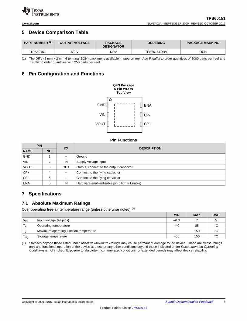
6 Pin Configuration and Functions
QFN Package6-Pin WSON
Top View
Pin FunctionsPIN
I/O DESCRIPTIONNAME NO.GND 1 – GroundVIN 2 IN Supply voltage inputVOUT 3 OUT Output, connect to the output capacitorCP+ 4 – Connect to the flying capacitorCP– 5 – Connect to the flying capacitorENA 6 IN Hardware enable/disable pin (High = Enable)
7 Specifications
7.1 Absolute Maximum RatingsOver operating free-air temperature range (unless otherwise noted) (1)
MIN MAX UNITVIN Input voltage (all pins) –0.3 7 VTA Operating temperature –40 85 °CTJ Maximum operating junction temperature 150 °CTstg Storage temperature –55 150 °C
(1) Stresses beyond those listed under Absolute Maximum Ratings may cause permanent damage to the device. These are stress ratingsonly and functional operation of the device at these or any other conditions beyond those indicated under Recommended OperatingConditions is not implied. Exposure to absolute-maximum-rated conditions for extended periods may affect device reliability.
Copyright © 2009–2015, Texas Instruments Incorporated Submit Documentation Feedback 3
Product Folder Links: TPS60151
TPS60151SLVSA02A –SEPTEMBER 2009–REVISED OCTOBER 2015 www.ti.com
7.2 ESD RatingsVALUE UNIT
Human body model (HBM), per ANSI/ESDA/JEDEC JS-001 (1) (2) ±2000V(ESD) Electrostatic discharge VCharged-device model (CDM), per JEDEC specification JESD22- ±500
C101 (3)
(1) JEDEC document JEP155 states that 500-V HBM allows safe manufacturing with a standard ESD control process.(2) The Human body model (HBM) is a 100 pF capacitor discharged through a 1.5 kΩ resistor into each pin. The testing is done according
JEDECs EIA/JESD22-A114.(3) JEDEC document JEP157 states that 250-V CDM allows safe manufacturing with a standard ESD control process.
7.3 Recommended Operating Conditionsover operating free-air temperature range (unless otherwise noted)
MIN NOM MAX UNITVIN Input voltage 2.7 5.5 VTA Operating ambient temperature -40 85 °CTJ Operating junction temperature -40 125 °CCIN Input capacitor 2.2 μFCOUT Output capacitor 2.2 μFCF Flying capacitor 1.0 μF
7.4 Thermal InformationTPS60151
THERMAL METRIC (1) DRV (WSON) UNIT6 PINS
RθJA Junction-to-ambient thermal resistance 69.1 °C/WRθJC(top) Junction-to-case (top) thermal resistance 79.8 °C/WRθJB Junction-to-board thermal resistance 38.6 °C/WψJT Junction-to-top characterization parameter 1.2 °C/WψJB Junction-to-board characterization parameter 38.4 °C/WRθJC(bot) Junction-to-case (bottom) thermal resistance 9.2 °C/W
(1) For more information about traditional and new thermal metrics, see the Semiconductor and IC Package Thermal Metrics applicationreport, SPRA953.
4 Submit Documentation Feedback Copyright © 2009–2015, Texas Instruments Incorporated
Product Folder Links: TPS60151
TPS60151www.ti.com SLVSA02A –SEPTEMBER 2009–REVISED OCTOBER 2015
7.5 Electrical CharacteristicsVIN = 3.6 V, TA = –40°C to 85°C, typical values are at TA = 25°C, C1 = C3 = 2.2 μF, C2 = 1.0 μF (unless otherwise noted)
PARAMETER TEST CONDITIONS MIN TYP MAX UNITPOWER STAGEVIN Input voltage range 2.7 5.5 VVUVLO Undervoltage lockout threshold 1.9 2.1 VIQ Operating quiescent current IOUT = 140 mA, Enable = VIN 4.7 mAIQskip Skip mode operating quiescent IOUT = 0 mA, Enable = VIN (no switching) 80 μA
current IOUT = 0 mA, Enable = VIN (minimum switching) 90 μAISD Shutdown current 2.7 V ≤ VIN ≤ 5.5 V, Enable = 0 V 4 10 μAVOUT Output voltage (1) IOUT ≤ 50 mA, 2.7 V ≤ VIN < 5.5V 4.8 5.0 5.2 VVOUT(skip) Skip mode output voltage IOUT = 0 mA, 2.7 V ≤ VIN ≤ 5.5 V VOUT+0.1 VFSW Switching frequency 1.5 MHztSS Soft-start time From the rising edge of enable to 90% output 150 μsOUTPUT CURRENTIOUT_nom Maximum output current VOUT remains between 4.8 V and 5.2 V, 120 mA
3.1 V ≤ VIN ≤ 5.5 V3.3 V < VIN < 5.5 V 140
IOUT_max Current limit VOUT = 4.5 V 500 mAIOUT_short Short circuit current (2) VOUT = 0 V 80 mARIPPLE VOLTAGEVR Output ripple voltage IOUT = 140 mA 30 mVENABLE CONTROLVHI Logic high input voltage 2.7 V ≤ VIN ≤ 5.5 V 1.3 VIN VVLI Logic low input voltage –0.2 0.4 VIHI Logic high input current 1 μAILI Logic low input current 1 μATHERMAL SHUTDOWNTSD Shutdown temperature 160 °CTRC Shutdown recovery 140 °C
(1) When in skip mode, output voltage can exceed VOUT spec because VOUT(skip)= VOUT +0.1.(2) TPS60151 has internal protection circuit to protect IC when VOUT shorted to GND.
Copyright © 2009–2015, Texas Instruments Incorporated Submit Documentation Feedback 5
Product Folder Links: TPS60151

0
0.05
0.1
0.15
0.2
0.25
0.3
2.7 3.2 3.7 4.2 4.7 5.2
V - Input Voltage - VI
I-
Max O
utp
ut
Cu
rren
t -
AO
T = -40°CA
T = 25°CAT = 85°CA
60
70
80
90
100
110
120
2.7 3.2 3.7 4.2 4.7 5.2
Inp
ut
Cu
rren
t -
Aµ
V - Input Voltage - VI
No loadNo Switching
-85 C°
-40 C°25 C°
TPS60151SLVSA02A –SEPTEMBER 2009–REVISED OCTOBER 2015 www.ti.com
7.6 Typical Characteristics
Figure 1. Quiescent Current vs Input Voltage Figure 2. Maximum Output Current vs Input Voltage atTemperature
6 Submit Documentation Feedback Copyright © 2009–2015, Texas Instruments Incorporated
Product Folder Links: TPS60151
VIN
OFF ON
ON OFF
VOUT
CF
COUT
+-2.5V
VQ1
Q1 Q2
Q3 Q4
VIN
OFF ON
ON OFF
VOUT
CF
COUT
+-2.5V
Q1 Q2
Q3 Q4
TPS60151www.ti.com SLVSA02A –SEPTEMBER 2009–REVISED OCTOBER 2015
8 Detailed Description
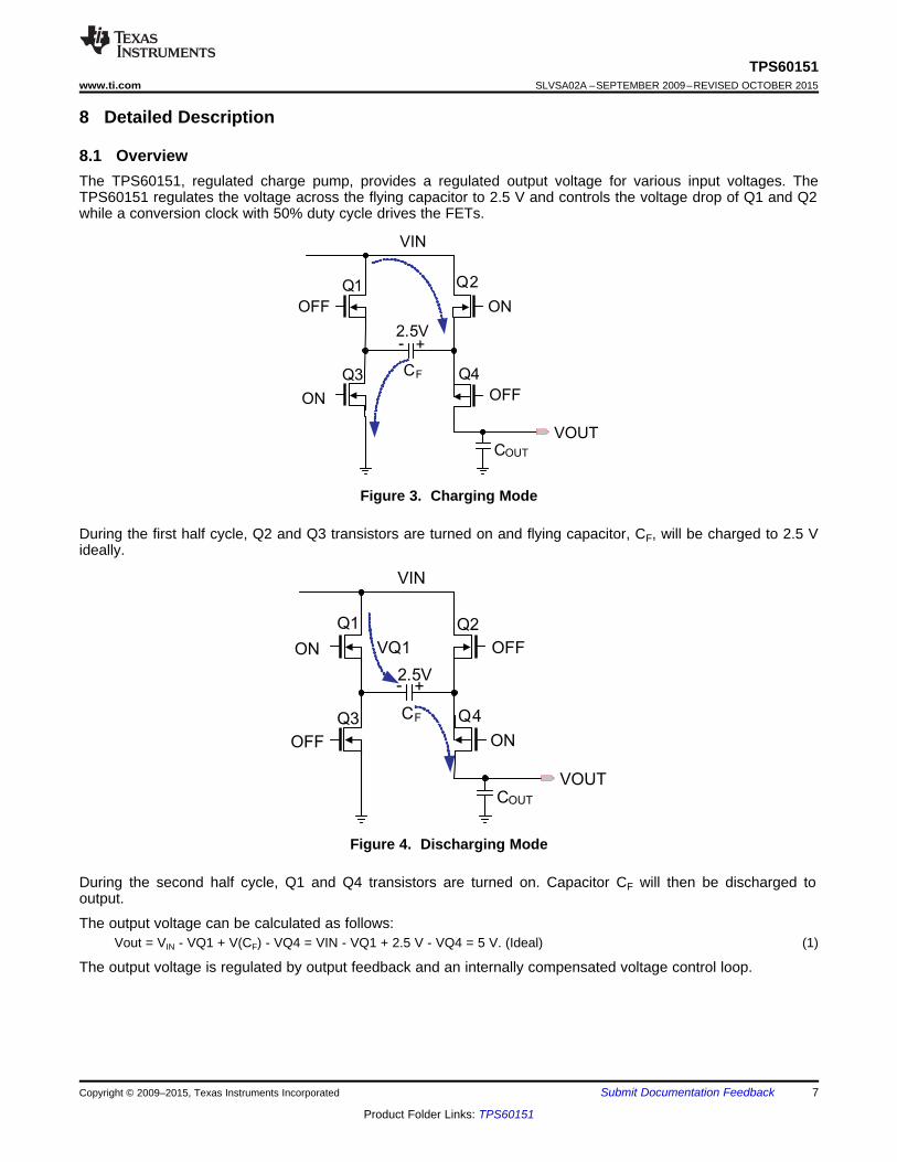
8.1 OverviewThe TPS60151, regulated charge pump, provides a regulated output voltage for various input voltages. TheTPS60151 regulates the voltage across the flying capacitor to 2.5 V and controls the voltage drop of Q1 and Q2while a conversion clock with 50% duty cycle drives the FETs.
Figure 3. Charging Mode
During the first half cycle, Q2 and Q3 transistors are turned on and flying capacitor, CF, will be charged to 2.5 Videally.
Figure 4. Discharging Mode
During the second half cycle, Q1 and Q4 transistors are turned on. Capacitor CF will then be discharged tooutput.
The output voltage can be calculated as follows:Vout = VIN - VQ1 + V(CF) - VQ4 = VIN - VQ1 + 2.5 V - VQ4 = 5 V. (Ideal) (1)
The output voltage is regulated by output feedback and an internally compensated voltage control loop.
Copyright © 2009–2015, Texas Instruments Incorporated Submit Documentation Feedback 7
Product Folder Links: TPS60151
CP-VIN
VOUT
GND
CP+
ENA
Ireverse
ENABLE/DISABLE
C2
1 Fm
C1
2.2 Fm
C3
2.2 FmVpre_bias
VIN
+
-
+
-
CP-
CF
CP+
Φ2
R1
R2
VOUT
ErrorAmp
Skip Comp
GND
VREF
TPS60151
Regulation
Current Limit
Soft Start
Enable IC
3
5 4
1
6
2VIN
ENA
Control
Bias circuit
TSD
UVLOΦ1
OSC1.5 MHz
Φ1 Φ2
TPS60151SLVSA02A –SEPTEMBER 2009–REVISED OCTOBER 2015 www.ti.com
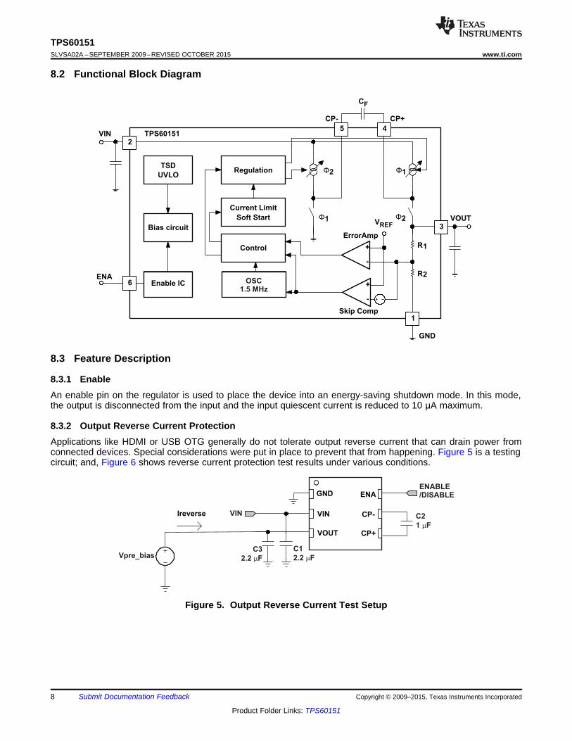
8.2 Functional Block Diagram
8.3 Feature Description
8.3.1 EnableAn enable pin on the regulator is used to place the device into an energy-saving shutdown mode. In this mode,the output is disconnected from the input and the input quiescent current is reduced to 10 μA maximum.
8.3.2 Output Reverse Current ProtectionApplications like HDMI or USB OTG generally do not tolerate output reverse current that can drain power fromconnected devices. Special considerations were put in place to prevent that from happening. Figure 5 is a testingcircuit; and, Figure 6 shows reverse current protection test results under various conditions.
Figure 5. Output Reverse Current Test Setup
8 Submit Documentation Feedback Copyright © 2009–2015, Texas Instruments Incorporated
Product Folder Links: TPS60151

-5
0
5
10
15
20
25
2.5 3 3.5 4 4.5 5 5.5Pre Bias Voltage - V
V = open/short, EN = 0/1IN
V = 3.6 V, EN = 0IN
V = 3.6 V, EN = 1IN
Revers
e C
urr
en
t -
Am
TPS60151www.ti.com SLVSA02A –SEPTEMBER 2009–REVISED OCTOBER 2015
Feature Description (continued)
Figure 6. Reverse Current Test Results (Typical)
8.3.3 Undervoltage LockoutWhen the input voltage drops, the undervoltage lockout prevents misoperation by switching off the device. Theconverter starts operation again when the input voltage exceeds the threshold, provided the enable pin is high.
8.3.4 Thermal Shutdown ProtectionThe regulator has thermal shutdown circuitry that protects it from damage caused by overload conditions. Thethermal protection circuitry disables the output when the junction temperature reached approximately 160°C,allowing the device to cool. When the junction temperature cools to approximately 140°C, the output circuitry isautomatically re-enabled. Continuously running the regulator into thermal shutdown can degrade reliability. Theregulator also provides current limit to protect itself and the load.
8.4 Device Functional Modes
8.4.1 Soft StartAn internal soft start limits the inrush current when the device is being enabled.
Copyright © 2009–2015, Texas Instruments Incorporated Submit Documentation Feedback 9
Product Folder Links: TPS60151
t
t
t
t
VOUT
Gate Waveform
Of Q1 Transistor
Load current
No load
Start up
Waveform
Skip Mode at
No Load Condition
Normal Mode at
50 mA Load Current
Skip Mode at
No Load Condition
Quiescent Current
90 Am
4.7 mA
50 mA
5 V +0.1 V5 V
TPS60151SLVSA02A –SEPTEMBER 2009–REVISED OCTOBER 2015 www.ti.com
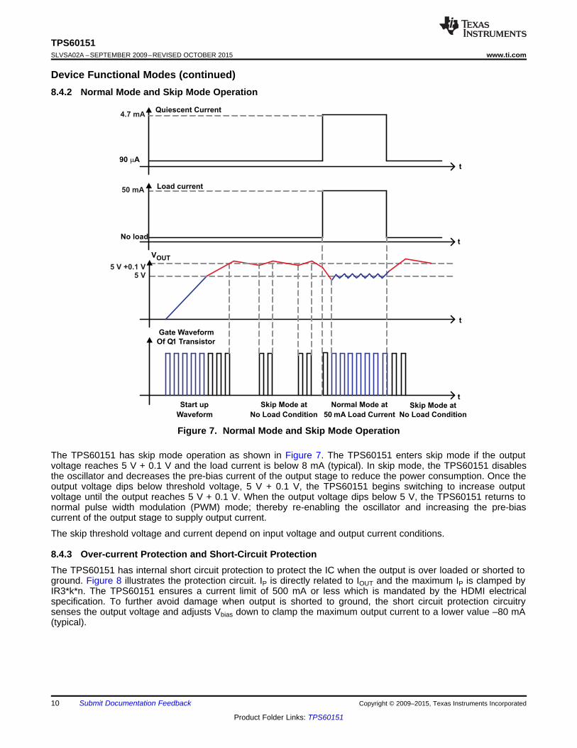
Device Functional Modes (continued)8.4.2 Normal Mode and Skip Mode Operation
Figure 7. Normal Mode and Skip Mode Operation
The TPS60151 has skip mode operation as shown in Figure 7. The TPS60151 enters skip mode if the outputvoltage reaches 5 V + 0.1 V and the load current is below 8 mA (typical). In skip mode, the TPS60151 disablesthe oscillator and decreases the pre-bias current of the output stage to reduce the power consumption. Once theoutput voltage dips below threshold voltage, 5 V + 0.1 V, the TPS60151 begins switching to increase outputvoltage until the output reaches 5 V + 0.1 V. When the output voltage dips below 5 V, the TPS60151 returns tonormal pulse width modulation (PWM) mode; thereby re-enabling the oscillator and increasing the pre-biascurrent of the output stage to supply output current.
The skip threshold voltage and current depend on input voltage and output current conditions.
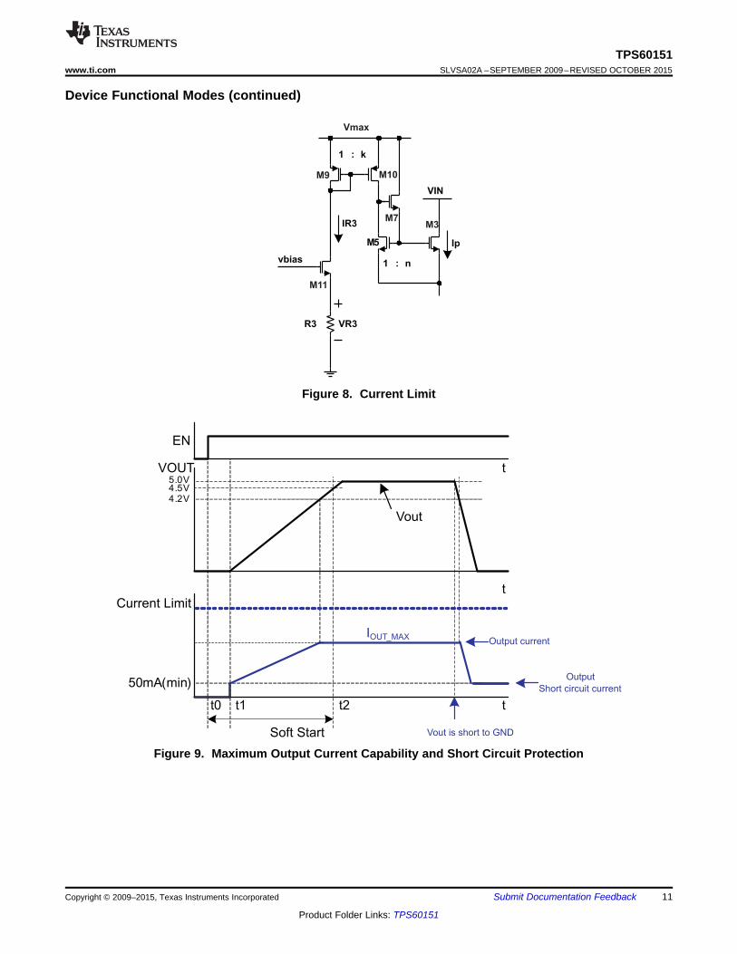
8.4.3 Over-current Protection and Short-Circuit ProtectionThe TPS60151 has internal short circuit protection to protect the IC when the output is over loaded or shorted toground. Figure 8 illustrates the protection circuit. IP is directly related to IOUT and the maximum IP is clamped byIR3*k*n. The TPS60151 ensures a current limit of 500 mA or less which is mandated by the HDMI electricalspecification. To further avoid damage when output is shorted to ground, the short circuit protection circuitrysenses the output voltage and adjusts Vbias down to clamp the maximum output current to a lower value –80 mA(typical).
10 Submit Documentation Feedback Copyright © 2009–2015, Texas Instruments Incorporated
Product Folder Links: TPS60151
VOUT
t
t
EN
t1 t2
Vout is short to GNDSoft Start
IOUT_MAX
50mA(min)
Current Limit
4.2V
Vout
t
t0
5.0V4.5V
Output
Short circuit current
Output current
R3 VR3
M5
VIN
1 : k
1 : n
IR3
Ip
vbias
Vmax
M9 M10
M7M3
M11
TPS60151www.ti.com SLVSA02A –SEPTEMBER 2009–REVISED OCTOBER 2015
Device Functional Modes (continued)
Figure 8. Current Limit
Figure 9. Maximum Output Current Capability and Short Circuit Protection
Copyright © 2009–2015, Texas Instruments Incorporated Submit Documentation Feedback 11
Product Folder Links: TPS60151
VBUS
GND
CP-VIN
VOUT
GND
CP+
ENA
USB
Transceiver
Controller
Comparator D+
ID
D-
VIN = 2.7 V - 5.5 V
C3
2.2 Fm
C1
2.2 Fm
C2
1 Fm
5 V
50mA (VIN > 2.7V)
140mA (VIN > 3.3V)
TPS60151SLVSA02A –SEPTEMBER 2009–REVISED OCTOBER 2015 www.ti.com
9 Application and Implementation
NOTEInformation in the following applications sections is not part of the TI componentspecification, and TI does not warrant its accuracy or completeness. TI’s customers areresponsible for determining suitability of components for their purposes. Customers shouldvalidate and test their design implementation to confirm system functionality.
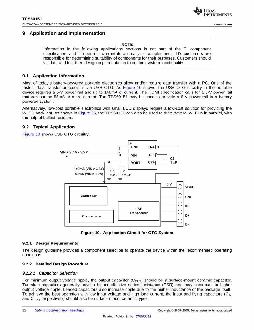
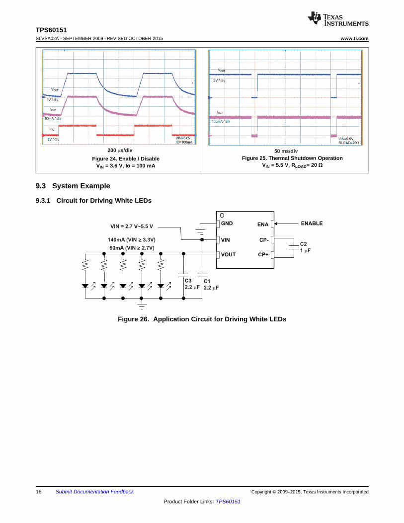
9.1 Application InformationMost of today’s battery-powered portable electronics allow and/or require data transfer with a PC. One of thefastest data transfer protocols is via USB OTG. As Figure 10 shows, the USB OTG circuitry in the portabledevice requires a 5-V power rail and up to 140mA of current. The HDMI specification calls for a 5-V power railthat can source 55mA or more current. The TPS60151 may be used to provide a 5-V power rail in a batterypowered system.
Alternatively, low-cost portable electronics with small LCD displays require a low-cost solution for providing theWLED backlight. As shown in Figure 26, the TPS60151 can also be used to drive several WLEDs in parallel, withthe help of ballast resistors.
9.2 Typical ApplicationFigure 10 shows USB OTG circuitry.
Figure 10. Application Circuit for OTG System
9.2.1 Design RequirementsThe design guideline provides a component selection to operate the device within the recommended operatingconditions.
9.2.2 Detailed Design Procedure
9.2.2.1 Capacitor SelectionFor minimum output voltage ripple, the output capacitor (COUT) should be a surface-mount ceramic capacitor.Tantalum capacitors generally have a higher effective series resistance (ESR) and may contribute to higheroutput voltage ripple. Leaded capacitors also increase ripple due to the higher inductance of the package itself.To achieve the best operation with low input voltage and high load current, the input and flying capacitors (CINand CFLY, respectively) should also be surface-mount ceramic types.
12 Submit Documentation Feedback Copyright © 2009–2015, Texas Instruments Incorporated
Product Folder Links: TPS60151
( )OUTIN OUT
IN
VEfficiency(%) = × 100 I = 2 I Quiescent current was neglected.
2 × V´
´
´ ´ = ´
´
OUT OUTIN OUT Q
IN IN
V IPD(out)Efficiency(%) = 100 = 100 , I 2 I + I
PD(in) V I
( )= + ´
´ ´
LOAD(MAX)OUT(RIPPLE) LOAD(MAX) COUT
OUT
IV 2I ESR
2 f C
æ ö´ ´ ç ÷
è ø\ ³D D ´ ¦
LOAD(MAX)LOAD(MAX)
FLYCFLY CFLY
T2 I
I2C =
V V
LOAD(MAX) FLY CFLY
T2 I = C V
2
æ ö\ ´ ´ ´ Dç ÷
è ø
charging FLY CFLY
discharging discharge LOAD(MAX)
Q = c v = C V ,
TQ = i t = 2 I , half duty.
2
´ ´ D
æ ö´ ´ ´ ç ÷
è ø
CP-VIN
VOUT
GND
CP+
ENA
VIN
VOUT(5 V)
ENABLE/DISABLE
COUT CIN
CFLY
TPS60151www.ti.com SLVSA02A –SEPTEMBER 2009–REVISED OCTOBER 2015
Typical Application (continued)
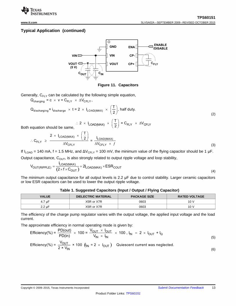
Figure 11. Capacitors
Generally, CFLY can be calculated by the following simple equation,
(2)
Both equation should be same,
(3)
If ILOAD = 140 mA, f = 1.5 MHz, and ΔVCFLY = 100 mV, the minimum value of the flying capacitor should be 1 μF.
Output capacitance, COUT, is also strongly related to output ripple voltage and loop stability,
(4)
The minimum output capacitance for all output levels is 2.2 μF due to control stability. Larger ceramic capacitorsor low ESR capacitors can be used to lower the output ripple voltage.
Table 1. Suggested Capacitors (Input / Output / Flying Capacitor)VALUE DIELECTRIC MATERIAL PACKAGE SIZE RATED VOLTAGE4.7 μF X5R or X7R 0603 10 V2.2 μF X5R or X7R 0603 10 V
The efficiency of the charge pump regulator varies with the output voltage, the applied input voltage and the loadcurrent.
The approximate efficiency in normal operating mode is given by:
(5)
(6)
Copyright © 2009–2015, Texas Instruments Incorporated Submit Documentation Feedback 13
Product Folder Links: TPS60151
5 ms/div
Vout
50 mV/div
CH1: BW = 200 MHzVIN = 2.7 V,
I = 0 mAO
20 s/divm
20 s/divm
2.7 3.2 3.7 4.2 4.7 5.2
V - Input Voltage - VI
0
10
20
30
40
50
60
70
80
90
100
Eff
icie
ncy -
%
10 mA
50 mA
150 mA
120 mA
100 mA
T = 25°CA
0 0.05 0.1 0.15 0.2
I - Output Current - AO
4.85
4.9
4.95
5
5.05
5.1
5.15
5.2
5.25V
- O
utp
ut
Vo
ltag
e -
VO
T = 25°CA
3.6 V 4.2 V
5 V 5.5 V
2.7 V
4.80
4.85
4.90
4.95
5.05
5.10
2.7 3.2 3.7 4.2 4.7 5.2
V-
Ou
tpu
t V
olt
ag
e -
VO
V - Input Voltage - VI
5.00
T = 25°CA
10 mA 50 mA
150 mA
120 mA
100 mA
TPS60151SLVSA02A –SEPTEMBER 2009–REVISED OCTOBER 2015 www.ti.com
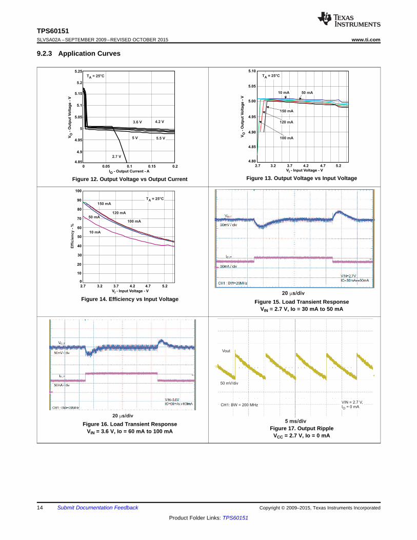
9.2.3 Application Curves
Figure 13. Output Voltage vs Input VoltageFigure 12. Output Voltage vs Output Current
Figure 14. Efficiency vs Input Voltage Figure 15. Load Transient ResponseVIN = 2.7 V, Io = 30 mA to 50 mA
Figure 16. Load Transient ResponseFigure 17. Output RippleVIN = 3.6 V, Io = 60 mA to 100 mA
VCC = 2.7 V, Io = 0 mA
14 Submit Documentation Feedback Copyright © 2009–2015, Texas Instruments Incorporated
Product Folder Links: TPS60151
200 s/divm1 ms/div
500 ns/div 1 ms/div
500 ns/div5 ms/div
Vout
50 mV/div
CH1: BW = 200 MHzVIN = 3.6 V,
I = 0 mAO
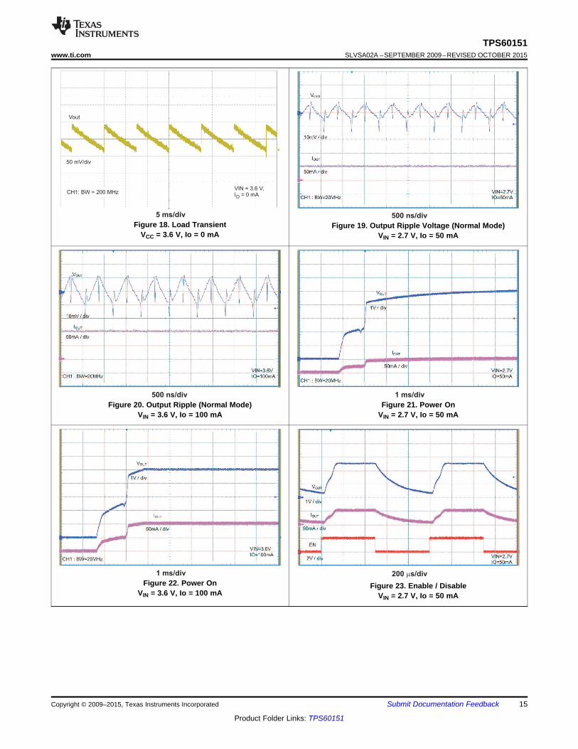
TPS60151www.ti.com SLVSA02A –SEPTEMBER 2009–REVISED OCTOBER 2015
Figure 18. Load Transient Figure 19. Output Ripple Voltage (Normal Mode)VCC = 3.6 V, Io = 0 mA VIN = 2.7 V, Io = 50 mA
Figure 20. Output Ripple (Normal Mode) Figure 21. Power OnVIN = 3.6 V, Io = 100 mA VIN = 2.7 V, Io = 50 mA
Figure 22. Power On Figure 23. Enable / DisableVIN = 3.6 V, Io = 100 mA VIN = 2.7 V, Io = 50 mA
Copyright © 2009–2015, Texas Instruments Incorporated Submit Documentation Feedback 15
Product Folder Links: TPS60151
CP-VIN
VOUT
GND
CP+
ENA ENABLEVIN = 2.7 V~5.5 V
C3
2.2 Fm
C1
2.2 Fm
C2
1 Fm50mA (VIN > 2.7V)
140mA (VIN > 3.3V)
200 s/divm 50 ms/div
TPS60151SLVSA02A –SEPTEMBER 2009–REVISED OCTOBER 2015 www.ti.com
Figure 25. Thermal Shutdown OperationFigure 24. Enable / DisableVIN = 5.5 V, RLOAD= 20 ΩVIN = 3.6 V, Io = 100 mA
9.3 System Example
9.3.1 Circuit for Driving White LEDs
Figure 26. Application Circuit for Driving White LEDs
16 Submit Documentation Feedback Copyright © 2009–2015, Texas Instruments Incorporated
Product Folder Links: TPS60151
GND
VIN
VOUT
GND
TPS60151www.ti.com SLVSA02A –SEPTEMBER 2009–REVISED OCTOBER 2015
10 Power Supply RecommendationsThe TPS60151 has no special requirements for its input power supply. The input power supply's output currentneeds to be rated according to the supply voltage, output voltage and output current of the TPS60151.
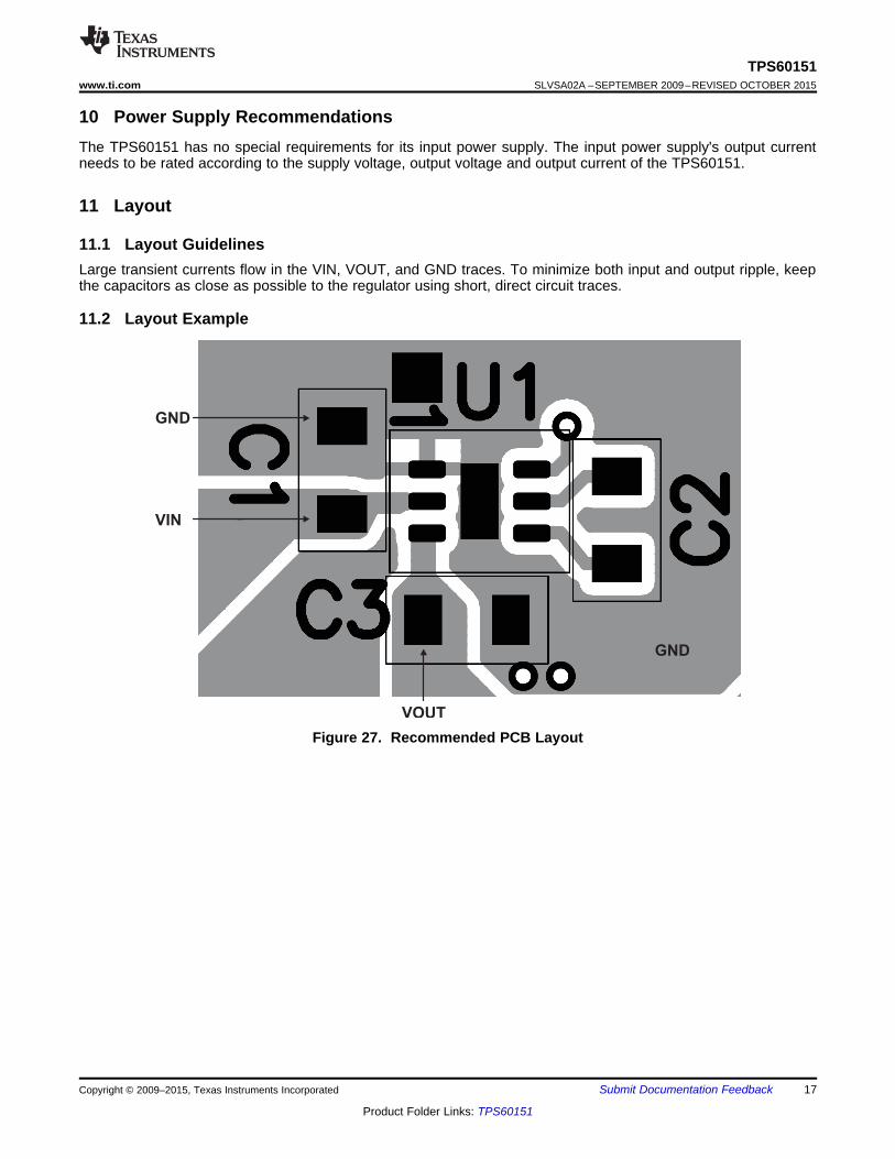
11 Layout
11.1 Layout GuidelinesLarge transient currents flow in the VIN, VOUT, and GND traces. To minimize both input and output ripple, keepthe capacitors as close as possible to the regulator using short, direct circuit traces.
11.2 Layout Example
Figure 27. Recommended PCB Layout
Copyright © 2009–2015, Texas Instruments Incorporated Submit Documentation Feedback 17
Product Folder Links: TPS60151
TPS60151SLVSA02A –SEPTEMBER 2009–REVISED OCTOBER 2015 www.ti.com
12 Device and Documentation Support
12.1 Community ResourcesThe following links connect to TI community resources. Linked contents are provided "AS IS" by the respectivecontributors. They do not constitute TI specifications and do not necessarily reflect TI's views; see TI's Terms ofUse.
TI E2E™ Online Community TI's Engineer-to-Engineer (E2E) Community. Created to foster collaborationamong engineers. At e2e.ti.com, you can ask questions, share knowledge, explore ideas and helpsolve problems with fellow engineers.
Design Support TI's Design Support Quickly find helpful E2E forums along with design support tools andcontact information for technical support.
12.2 TrademarksE2E is a trademark of Texas Instruments.All other trademarks are the property of their respective owners.
12.3 Electrostatic Discharge CautionThese devices have limited built-in ESD protection. The leads should be shorted together or the device placed in conductive foamduring storage or handling to prevent electrostatic damage to the MOS gates.
12.4 GlossarySLYZ022 — TI Glossary.
This glossary lists and explains terms, acronyms, and definitions.
13 Mechanical, Packaging, and Orderable InformationThe following pages include mechanical, packaging, and orderable information. This information is the mostcurrent data available for the designated devices. This data is subject to change without notice and revision ofthis document. For browser-based versions of this data sheet, refer to the left-hand navigation.
18 Submit Documentation Feedback Copyright © 2009–2015, Texas Instruments Incorporated
Product Folder Links: TPS60151
PACKAGE OPTION ADDENDUM
www.ti.com 11-Jul-2018
Addendum-Page 1
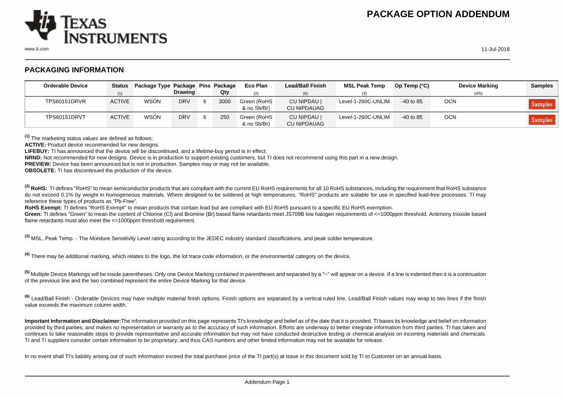
PACKAGING INFORMATION
Orderable Device Status(1)
Package Type PackageDrawing
Pins PackageQty
Eco Plan(2)
Lead/Ball Finish(6)
MSL Peak Temp(3)
Op Temp (°C) Device Marking(4/5)
Samples
TPS60151DRVR ACTIVE WSON DRV 6 3000 Green (RoHS& no Sb/Br)
CU NIPDAU |CU NIPDAUAG
Level-1-260C-UNLIM -40 to 85 OCN
TPS60151DRVT ACTIVE WSON DRV 6 250 Green (RoHS& no Sb/Br)
CU NIPDAU |CU NIPDAUAG
Level-1-260C-UNLIM -40 to 85 OCN
(1) The marketing status values are defined as follows:ACTIVE: Product device recommended for new designs.LIFEBUY: TI has announced that the device will be discontinued, and a lifetime-buy period is in effect.NRND: Not recommended for new designs. Device is in production to support existing customers, but TI does not recommend using this part in a new design.PREVIEW: Device has been announced but is not in production. Samples may or may not be available.OBSOLETE: TI has discontinued the production of the device.
(2) RoHS: TI defines "RoHS" to mean semiconductor products that are compliant with the current EU RoHS requirements for all 10 RoHS substances, including the requirement that RoHS substancedo not exceed 0.1% by weight in homogeneous materials. Where designed to be soldered at high temperatures, "RoHS" products are suitable for use in specified lead-free processes. TI mayreference these types of products as "Pb-Free".RoHS Exempt: TI defines "RoHS Exempt" to mean products that contain lead but are compliant with EU RoHS pursuant to a specific EU RoHS exemption.Green: TI defines "Green" to mean the content of Chlorine (Cl) and Bromine (Br) based flame retardants meet JS709B low halogen requirements of <=1000ppm threshold. Antimony trioxide basedflame retardants must also meet the <=1000ppm threshold requirement.
(3) MSL, Peak Temp. - The Moisture Sensitivity Level rating according to the JEDEC industry standard classifications, and peak solder temperature.
(4) There may be additional marking, which relates to the logo, the lot trace code information, or the environmental category on the device.
(5) Multiple Device Markings will be inside parentheses. Only one Device Marking contained in parentheses and separated by a "~" will appear on a device. If a line is indented then it is a continuationof the previous line and the two combined represent the entire Device Marking for that device.
(6) Lead/Ball Finish - Orderable Devices may have multiple material finish options. Finish options are separated by a vertical ruled line. Lead/Ball Finish values may wrap to two lines if the finishvalue exceeds the maximum column width.
Important Information and Disclaimer:The information provided on this page represents TI's knowledge and belief as of the date that it is provided. TI bases its knowledge and belief on informationprovided by third parties, and makes no representation or warranty as to the accuracy of such information. Efforts are underway to better integrate information from third parties. TI has taken andcontinues to take reasonable steps to provide representative and accurate information but may not have conducted destructive testing or chemical analysis on incoming materials and chemicals.TI and TI suppliers consider certain information to be proprietary, and thus CAS numbers and other limited information may not be available for release.
In no event shall TI's liability arising out of such information exceed the total purchase price of the TI part(s) at issue in this document sold by TI to Customer on an annual basis.
PACKAGE OPTION ADDENDUM
www.ti.com 11-Jul-2018
Addendum-Page 2
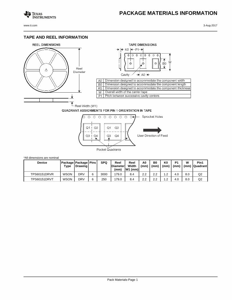
TAPE AND REEL INFORMATION
*All dimensions are nominal
Device PackageType
PackageDrawing
Pins SPQ ReelDiameter
(mm)
ReelWidth
W1 (mm)
A0(mm)
B0(mm)
K0(mm)
P1(mm)
W(mm)
Pin1Quadrant
TPS60151DRVR WSON DRV 6 3000 179.0 8.4 2.2 2.2 1.2 4.0 8.0 Q2
TPS60151DRVT WSON DRV 6 250 179.0 8.4 2.2 2.2 1.2 4.0 8.0 Q2
PACKAGE MATERIALS INFORMATION
www.ti.com 3-Aug-2017
Pack Materials-Page 1
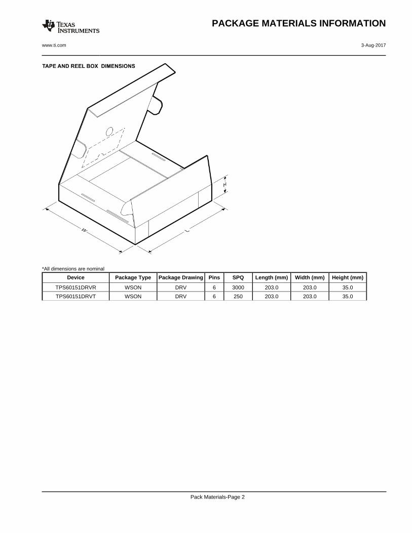
*All dimensions are nominal
Device Package Type Package Drawing Pins SPQ Length (mm) Width (mm) Height (mm)
TPS60151DRVR WSON DRV 6 3000 203.0 203.0 35.0
TPS60151DRVT WSON DRV 6 250 203.0 203.0 35.0
PACKAGE MATERIALS INFORMATION
www.ti.com 3-Aug-2017
Pack Materials-Page 2
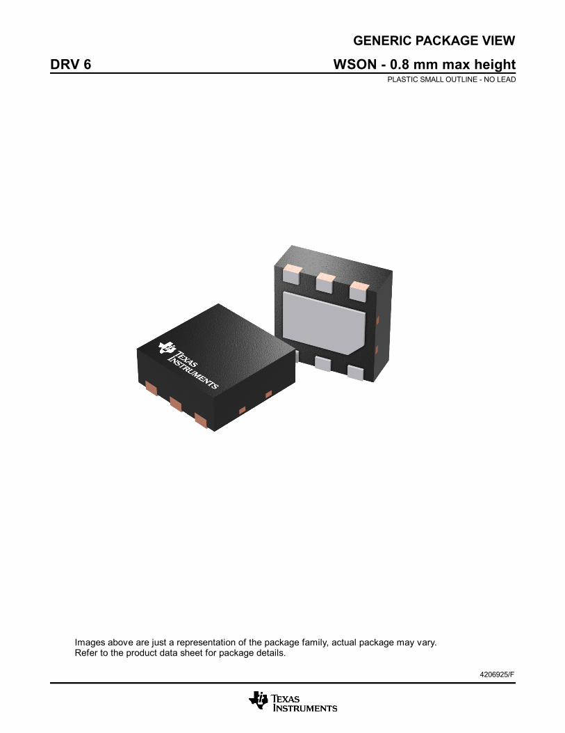
GENERIC PACKAGE VIEW
Images above are just a representation of the package family, actual package may vary.Refer to the product data sheet for package details.
DRV 6 WSON - 0.8 mm max heightPLASTIC SMALL OUTLINE - NO LEAD
4206925/F
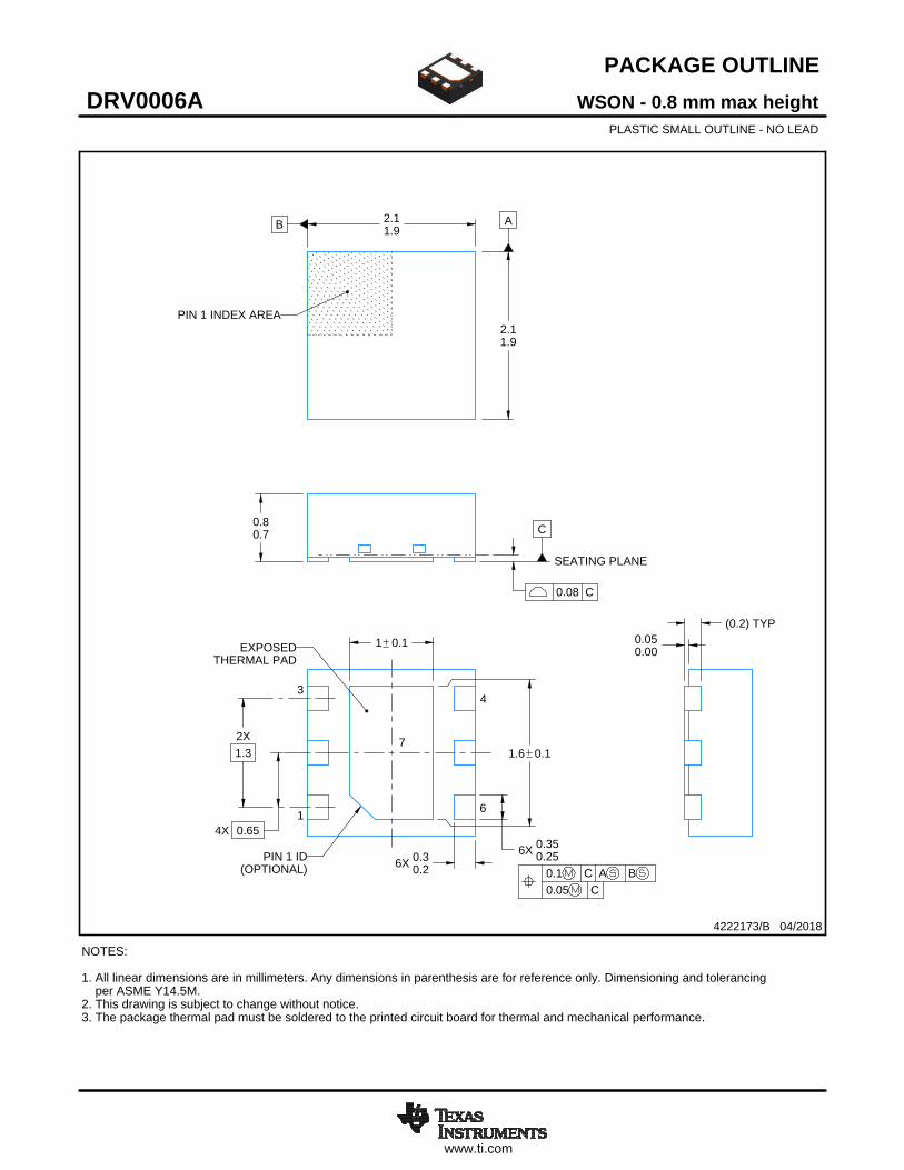
www.ti.com
PACKAGE OUTLINE
C
6X 0.350.25
1.6 0.1
6X 0.30.2
2X1.3
1 0.1
4X 0.65
0.80.7
0.050.00
B 2.11.9
A
2.11.9
(0.2) TYP
WSON - 0.8 mm max heightDRV0006APLASTIC SMALL OUTLINE - NO LEAD
4222173/B 04/2018
PIN 1 INDEX AREA
SEATING PLANE
0.08 C
1
34
6
(OPTIONAL)PIN 1 ID
0.1 C A B0.05 C
THERMAL PADEXPOSED
7
NOTES: 1. All linear dimensions are in millimeters. Any dimensions in parenthesis are for reference only. Dimensioning and tolerancing per ASME Y14.5M. 2. This drawing is subject to change without notice. 3. The package thermal pad must be soldered to the printed circuit board for thermal and mechanical performance.
SCALE 5.500

www.ti.com
EXAMPLE BOARD LAYOUT
0.07 MINALL AROUND
0.07 MAXALL AROUND
(1)
4X (0.65)
(1.95)
6X (0.3)
6X (0.45)
(1.6)
(R0.05) TYP
( 0.2) VIATYP
(1.1)
WSON - 0.8 mm max heightDRV0006APLASTIC SMALL OUTLINE - NO LEAD
4222173/B 04/2018
SYMM
1
34
6
SYMM
LAND PATTERN EXAMPLESCALE:25X
7
NOTES: (continued) 4. This package is designed to be soldered to a thermal pad on the board. For more information, see Texas Instruments literature number SLUA271 (www.ti.com/lit/slua271).5. Vias are optional depending on application, refer to device data sheet. If some or all are implemented, recommended via locations are shown.
SOLDER MASKOPENINGSOLDER MASK
METAL UNDER
SOLDER MASKDEFINED
METALSOLDER MASKOPENING
SOLDER MASK DETAILS
NON SOLDER MASKDEFINED
(PREFERRED)
www.ti.com
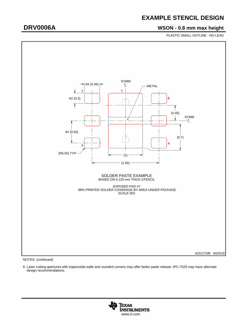
EXAMPLE STENCIL DESIGN
6X (0.3)
6X (0.45)
4X (0.65)
(0.7)
(1)
(1.95)
(R0.05) TYP
(0.45)
WSON - 0.8 mm max heightDRV0006APLASTIC SMALL OUTLINE - NO LEAD
4222173/B 04/2018
NOTES: (continued) 6. Laser cutting apertures with trapezoidal walls and rounded corners may offer better paste release. IPC-7525 may have alternate design recommendations.
SOLDER PASTE EXAMPLEBASED ON 0.125 mm THICK STENCIL
EXPOSED PAD #7
88% PRINTED SOLDER COVERAGE BY AREA UNDER PACKAGESCALE:30X
SYMM
1
3 4
6
SYMM
METAL7
IMPORTANT NOTICE
Texas Instruments Incorporated (TI) reserves the right to make corrections, enhancements, improvements and other changes to itssemiconductor products and services per JESD46, latest issue, and to discontinue any product or service per JESD48, latest issue. Buyersshould obtain the latest relevant information before placing orders and should verify that such information is current and complete.TI’s published terms of sale for semiconductor products (http://www.ti.com/sc/docs/stdterms.htm) apply to the sale of packaged integratedcircuit products that TI has qualified and released to market. Additional terms may apply to the use or sale of other types of TI products andservices.Reproduction of significant portions of TI information in TI data sheets is permissible only if reproduction is without alteration and isaccompanied by all associated warranties, conditions, limitations, and notices. TI is not responsible or liable for such reproduceddocumentation. Information of third parties may be subject to additional restrictions. Resale of TI products or services with statementsdifferent from or beyond the parameters stated by TI for that product or service voids all express and any implied warranties for theassociated TI product or service and is an unfair and deceptive business practice. TI is not responsible or liable for any such statements.Buyers and others who are developing systems that incorporate TI products (collectively, “Designers”) understand and agree that Designersremain responsible for using their independent analysis, evaluation and judgment in designing their applications and that Designers havefull and exclusive responsibility to assure the safety of Designers' applications and compliance of their applications (and of all TI productsused in or for Designers’ applications) with all applicable regulations, laws and other applicable requirements. Designer represents that, withrespect to their applications, Designer has all the necessary expertise to create and implement safeguards that (1) anticipate dangerousconsequences of failures, (2) monitor failures and their consequences, and (3) lessen the likelihood of failures that might cause harm andtake appropriate actions. Designer agrees that prior to using or distributing any applications that include TI products, Designer willthoroughly test such applications and the functionality of such TI products as used in such applications.TI’s provision of technical, application or other design advice, quality characterization, reliability data or other services or information,including, but not limited to, reference designs and materials relating to evaluation modules, (collectively, “TI Resources”) are intended toassist designers who are developing applications that incorporate TI products; by downloading, accessing or using TI Resources in anyway, Designer (individually or, if Designer is acting on behalf of a company, Designer’s company) agrees to use any particular TI Resourcesolely for this purpose and subject to the terms of this Notice.TI’s provision of TI Resources does not expand or otherwise alter TI’s applicable published warranties or warranty disclaimers for TIproducts, and no additional obligations or liabilities arise from TI providing such TI Resources. TI reserves the right to make corrections,enhancements, improvements and other changes to its TI Resources. TI has not conducted any testing other than that specificallydescribed in the published documentation for a particular TI Resource.Designer is authorized to use, copy and modify any individual TI Resource only in connection with the development of applications thatinclude the TI product(s) identified in such TI Resource. NO OTHER LICENSE, EXPRESS OR IMPLIED, BY ESTOPPEL OR OTHERWISETO ANY OTHER TI INTELLECTUAL PROPERTY RIGHT, AND NO LICENSE TO ANY TECHNOLOGY OR INTELLECTUAL PROPERTYRIGHT OF TI OR ANY THIRD PARTY IS GRANTED HEREIN, including but not limited to any patent right, copyright, mask work right, orother intellectual property right relating to any combination, machine, or process in which TI products or services are used. Informationregarding or referencing third-party products or services does not constitute a license to use such products or services, or a warranty orendorsement thereof. Use of TI Resources may require a license from a third party under the patents or other intellectual property of thethird party, or a license from TI under the patents or other intellectual property of TI.TI RESOURCES ARE PROVIDED “AS IS” AND WITH ALL FAULTS. TI DISCLAIMS ALL OTHER WARRANTIES ORREPRESENTATIONS, EXPRESS OR IMPLIED, REGARDING RESOURCES OR USE THEREOF, INCLUDING BUT NOT LIMITED TOACCURACY OR COMPLETENESS, TITLE, ANY EPIDEMIC FAILURE WARRANTY AND ANY IMPLIED WARRANTIES OFMERCHANTABILITY, FITNESS FOR A PARTICULAR PURPOSE, AND NON-INFRINGEMENT OF ANY THIRD PARTY INTELLECTUALPROPERTY RIGHTS. TI SHALL NOT BE LIABLE FOR AND SHALL NOT DEFEND OR INDEMNIFY DESIGNER AGAINST ANY CLAIM,INCLUDING BUT NOT LIMITED TO ANY INFRINGEMENT CLAIM THAT RELATES TO OR IS BASED ON ANY COMBINATION OFPRODUCTS EVEN IF DESCRIBED IN TI RESOURCES OR OTHERWISE. IN NO EVENT SHALL TI BE LIABLE FOR ANY ACTUAL,DIRECT, SPECIAL, COLLATERAL, INDIRECT, PUNITIVE, INCIDENTAL, CONSEQUENTIAL OR EXEMPLARY DAMAGES INCONNECTION WITH OR ARISING OUT OF TI RESOURCES OR USE THEREOF, AND REGARDLESS OF WHETHER TI HAS BEENADVISED OF THE POSSIBILITY OF SUCH DAMAGES.Unless TI has explicitly designated an individual product as meeting the requirements of a particular industry standard (e.g., ISO/TS 16949and ISO 26262), TI is not responsible for any failure to meet such industry standard requirements.Where TI specifically promotes products as facilitating functional safety or as compliant with industry functional safety standards, suchproducts are intended to help enable customers to design and create their own applications that meet applicable functional safety standardsand requirements. Using products in an application does not by itself establish any safety features in the application. Designers mustensure compliance with safety-related requirements and standards applicable to their applications. Designer may not use any TI products inlife-critical medical equipment unless authorized officers of the parties have executed a special contract specifically governing such use.Life-critical medical equipment is medical equipment where failure of such equipment would cause serious bodily injury or death (e.g., lifesupport, pacemakers, defibrillators, heart pumps, neurostimulators, and implantables). Such equipment includes, without limitation, allmedical devices identified by the U.S. Food and Drug Administration as Class III devices and equivalent classifications outside the U.S.TI may expressly designate certain products as completing a particular qualification (e.g., Q100, Military Grade, or Enhanced Product).Designers agree that it has the necessary expertise to select the product with the appropriate qualification designation for their applicationsand that proper product selection is at Designers’ own risk. Designers are solely responsible for compliance with all legal and regulatoryrequirements in connection with such selection.Designer will fully indemnify TI and its representatives against any damages, costs, losses, and/or liabilities arising out of Designer’s non-compliance with the terms and provisions of this Notice.
Mailing Address: Texas Instruments, Post Office Box 655303, Dallas, Texas 75265Copyright © 2018, Texas Instruments Incorporated