TPL9032 Series 300-mA High PSRR, Ultra-low Noise LDO
19
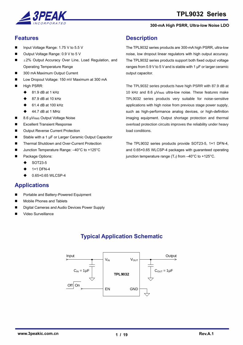
www.3peakic.com.cn Rev.A.1 1 / 19 TPL9032 Series 300-mA High PSRR, Ultra-low Noise LDO Features ◼ Input Voltage Range: 1.75 V to 5.5 V ◼ Output Voltage Range: 0.9 V to 5 V ◼ ±2% Output Accuracy Over Line, Load Regulation, and Operating Temperature Range ◼ 300 mA Maximum Output Current ◼ Low Dropout Voltage: 150 mV Maximum at 300 mA ◼ High PSRR: ◆ 81.9 dB at 1 kHz ◆ 87.9 dB at 10 kHz ◆ 61.4 dB at 100 kHz ◆ 44.7 dB at 1 MHz ◼ 8.6 μVRMS Output Voltage Noise ◼ Excellent Transient Response ◼ Output Reverse Current Protection ◼ Stable with a 1 μF or Larger Ceramic Output Capacitor ◼ Thermal Shutdown and Over-Current Protection ◼ Junction Temperature Range: –40°C to +125°C ◼ Package Options: ◆ SOT23-5 ◆ 1×1 DFN-4 ◆ 0.65×0.65 WLCSP-4 Applications ◼ Portable and Battery-Powered Equipment ◼ Mobile Phones and Tablets ◼ Digital Cameras and Audio Devices Power Supply ◼ Video Surveillance Description The TPL9032 series products are 300-mA high PSRR, ultra-low noise, low dropout linear regulators with high output accuracy. The TPL9032 series products support both fixed output voltage ranges from 0.9 V to 5 V and is stable with 1 μF or larger ceramic output capacitor. The TPL9032 series products have high PSRR with 87.9 dB at 10 kHz and 8.6 μVRMS ultra-low noise. These features make TPL9032 series products very suitable for noise-sensitive applications with high noise from previous stage power supply, such as high-performance analog devices, or high-definition imaging equipment. Output shortage protection and thermal overload protection circuits improves the reliability under heavy load conditions. The TPL9032 series products provide SOT23-5, 1×1 DFN-4, and 0.65×0.65 WLCSP-4 packages with guaranteed operating junction temperature range (TJ) from –40°C to +125°C. Typical Application Schematic V IN V OUT EN GND Input Off On TPL9032 C OUT = 1μF Output C IN = 1μF
Transcript of TPL9032 Series 300-mA High PSRR, Ultra-low Noise LDO
www.3peakic.com.cn Rev.A.1
1 / 19
TPL9032 Series
300-mA High PSRR, Ultra-low Noise LDO
Features
◼ Input Voltage Range: 1.75 V to 5.5 V
◼ Output Voltage Range: 0.9 V to 5 V
◼ ±2% Output Accuracy Over Line, Load Regulation, and
Operating Temperature Range
◼ 300 mA Maximum Output Current
◼ Low Dropout Voltage: 150 mV Maximum at 300 mA
◼ High PSRR:
81.9 dB at 1 kHz
87.9 dB at 10 kHz
61.4 dB at 100 kHz
44.7 dB at 1 MHz
◼ 8.6 μVRMS Output Voltage Noise
◼ Excellent Transient Response
◼ Output Reverse Current Protection
◼ Stable with a 1 μF or Larger Ceramic Output Capacitor
◼ Thermal Shutdown and Over-Current Protection
◼ Junction Temperature Range: –40°C to +125°C
◼ Package Options:
SOT23-5
1×1 DFN-4
0.65×0.65 WLCSP-4
Applications
◼ Portable and Battery-Powered Equipment
◼ Mobile Phones and Tablets
◼ Digital Cameras and Audio Devices Power Supply
◼ Video Surveillance
Description
The TPL9032 series products are 300-mA high PSRR, ultra-low
noise, low dropout linear regulators with high output accuracy.
The TPL9032 series products support both fixed output voltage
ranges from 0.9 V to 5 V and is stable with 1 μF or larger ceramic
output capacitor.
The TPL9032 series products have high PSRR with 87.9 dB at
10 kHz and 8.6 μVRMS ultra-low noise. These features make
TPL9032 series products very suitable for noise-sensitive
applications with high noise from previous stage power supply,
such as high-performance analog devices, or high-definition
imaging equipment. Output shortage protection and thermal
overload protection circuits improves the reliability under heavy
load conditions.
The TPL9032 series products provide SOT23-5, 1×1 DFN-4,
and 0.65×0.65 WLCSP-4 packages with guaranteed operating
junction temperature range (TJ) from –40°C to +125°C.
Typical Application Schematic
VIN VOUT
EN GND
Input
Off On
TPL9032COUT = 1µF
Output
CIN = 1µF
www.3peakic.com.cn Rev.A.1
2 / 19
TPL9032 Series
300-mA High PSRR, Ultra-low Noise LDO
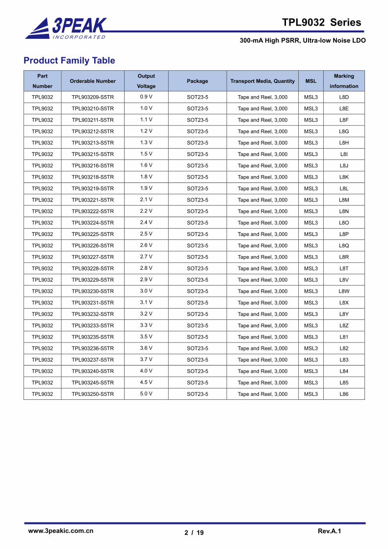
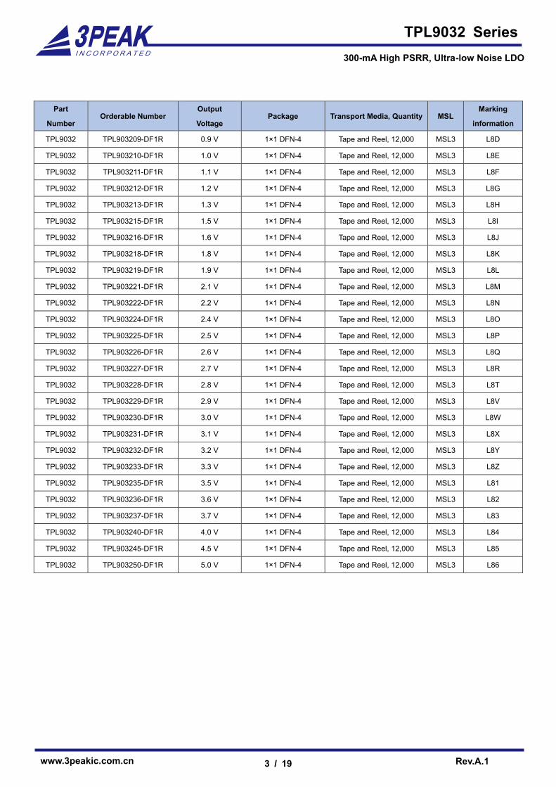
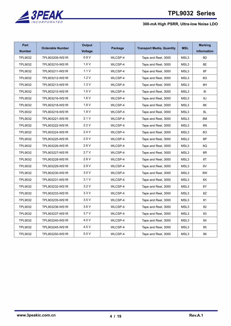
Product Family Table
Part
Number Orderable Number
Output
Voltage Package Transport Media, Quantity MSL
Marking
information
TPL9032 TPL903209-S5TR 0.9 V SOT23-5 Tape and Reel, 3,000 MSL3 L8D
TPL9032 TPL903210-S5TR 1.0 V SOT23-5 Tape and Reel, 3,000 MSL3 L8E
TPL9032 TPL903211-S5TR 1.1 V SOT23-5 Tape and Reel, 3,000 MSL3 L8F
TPL9032 TPL903212-S5TR 1.2 V SOT23-5 Tape and Reel, 3,000 MSL3 L8G
TPL9032 TPL903213-S5TR 1.3 V SOT23-5 Tape and Reel, 3,000 MSL3 L8H
TPL9032 TPL903215-S5TR 1.5 V SOT23-5 Tape and Reel, 3,000 MSL3 L8I
TPL9032 TPL903216-S5TR 1.6 V SOT23-5 Tape and Reel, 3,000 MSL3 L8J
TPL9032 TPL903218-S5TR 1.8 V SOT23-5 Tape and Reel, 3,000 MSL3 L8K
TPL9032 TPL903219-S5TR 1.9 V SOT23-5 Tape and Reel, 3,000 MSL3 L8L
TPL9032 TPL903221-S5TR 2.1 V SOT23-5 Tape and Reel, 3,000 MSL3 L8M
TPL9032 TPL903222-S5TR 2.2 V SOT23-5 Tape and Reel, 3,000 MSL3 L8N
TPL9032 TPL903224-S5TR 2.4 V SOT23-5 Tape and Reel, 3,000 MSL3 L8O
TPL9032 TPL903225-S5TR 2.5 V SOT23-5 Tape and Reel, 3,000 MSL3 L8P
TPL9032 TPL903226-S5TR 2.6 V SOT23-5 Tape and Reel, 3,000 MSL3 L8Q
TPL9032 TPL903227-S5TR 2.7 V SOT23-5 Tape and Reel, 3,000 MSL3 L8R
TPL9032 TPL903228-S5TR 2.8 V SOT23-5 Tape and Reel, 3,000 MSL3 L8T
TPL9032 TPL903229-S5TR 2.9 V SOT23-5 Tape and Reel, 3,000 MSL3 L8V
TPL9032 TPL903230-S5TR 3.0 V SOT23-5 Tape and Reel, 3,000 MSL3 L8W
TPL9032 TPL903231-S5TR 3.1 V SOT23-5 Tape and Reel, 3,000 MSL3 L8X
TPL9032 TPL903232-S5TR 3.2 V SOT23-5 Tape and Reel, 3,000 MSL3 L8Y
TPL9032 TPL903233-S5TR 3.3 V SOT23-5 Tape and Reel, 3,000 MSL3 L8Z
TPL9032 TPL903235-S5TR 3.5 V SOT23-5 Tape and Reel, 3,000 MSL3 L81
TPL9032 TPL903236-S5TR 3.6 V SOT23-5 Tape and Reel, 3,000 MSL3 L82
TPL9032 TPL903237-S5TR 3.7 V SOT23-5 Tape and Reel, 3,000 MSL3 L83
TPL9032 TPL903240-S5TR 4.0 V SOT23-5 Tape and Reel, 3,000 MSL3 L84
TPL9032 TPL903245-S5TR 4.5 V SOT23-5 Tape and Reel, 3,000 MSL3 L85
TPL9032 TPL903250-S5TR 5.0 V SOT23-5 Tape and Reel, 3,000 MSL3 L86
www.3peakic.com.cn Rev.A.1
3 / 19
TPL9032 Series
300-mA High PSRR, Ultra-low Noise LDO
Part
Number Orderable Number
Output
Voltage Package Transport Media, Quantity MSL
Marking
information
TPL9032 TPL903209-DF1R 0.9 V 1×1 DFN-4 Tape and Reel, 12,000 MSL3 L8D
TPL9032 TPL903210-DF1R 1.0 V 1×1 DFN-4 Tape and Reel, 12,000 MSL3 L8E
TPL9032 TPL903211-DF1R 1.1 V 1×1 DFN-4 Tape and Reel, 12,000 MSL3 L8F
TPL9032 TPL903212-DF1R 1.2 V 1×1 DFN-4 Tape and Reel, 12,000 MSL3 L8G
TPL9032 TPL903213-DF1R 1.3 V 1×1 DFN-4 Tape and Reel, 12,000 MSL3 L8H
TPL9032 TPL903215-DF1R 1.5 V 1×1 DFN-4 Tape and Reel, 12,000 MSL3 L8I
TPL9032 TPL903216-DF1R 1.6 V 1×1 DFN-4 Tape and Reel, 12,000 MSL3 L8J
TPL9032 TPL903218-DF1R 1.8 V 1×1 DFN-4 Tape and Reel, 12,000 MSL3 L8K
TPL9032 TPL903219-DF1R 1.9 V 1×1 DFN-4 Tape and Reel, 12,000 MSL3 L8L
TPL9032 TPL903221-DF1R 2.1 V 1×1 DFN-4 Tape and Reel, 12,000 MSL3 L8M
TPL9032 TPL903222-DF1R 2.2 V 1×1 DFN-4 Tape and Reel, 12,000 MSL3 L8N
TPL9032 TPL903224-DF1R 2.4 V 1×1 DFN-4 Tape and Reel, 12,000 MSL3 L8O
TPL9032 TPL903225-DF1R 2.5 V 1×1 DFN-4 Tape and Reel, 12,000 MSL3 L8P
TPL9032 TPL903226-DF1R 2.6 V 1×1 DFN-4 Tape and Reel, 12,000 MSL3 L8Q
TPL9032 TPL903227-DF1R 2.7 V 1×1 DFN-4 Tape and Reel, 12,000 MSL3 L8R
TPL9032 TPL903228-DF1R 2.8 V 1×1 DFN-4 Tape and Reel, 12,000 MSL3 L8T
TPL9032 TPL903229-DF1R 2.9 V 1×1 DFN-4 Tape and Reel, 12,000 MSL3 L8V
TPL9032 TPL903230-DF1R 3.0 V 1×1 DFN-4 Tape and Reel, 12,000 MSL3 L8W
TPL9032 TPL903231-DF1R 3.1 V 1×1 DFN-4 Tape and Reel, 12,000 MSL3 L8X
TPL9032 TPL903232-DF1R 3.2 V 1×1 DFN-4 Tape and Reel, 12,000 MSL3 L8Y
TPL9032 TPL903233-DF1R 3.3 V 1×1 DFN-4 Tape and Reel, 12,000 MSL3 L8Z
TPL9032 TPL903235-DF1R 3.5 V 1×1 DFN-4 Tape and Reel, 12,000 MSL3 L81
TPL9032 TPL903236-DF1R 3.6 V 1×1 DFN-4 Tape and Reel, 12,000 MSL3 L82
TPL9032 TPL903237-DF1R 3.7 V 1×1 DFN-4 Tape and Reel, 12,000 MSL3 L83
TPL9032 TPL903240-DF1R 4.0 V 1×1 DFN-4 Tape and Reel, 12,000 MSL3 L84
TPL9032 TPL903245-DF1R 4.5 V 1×1 DFN-4 Tape and Reel, 12,000 MSL3 L85
TPL9032 TPL903250-DF1R 5.0 V 1×1 DFN-4 Tape and Reel, 12,000 MSL3 L86
www.3peakic.com.cn Rev.A.1
4 / 19
TPL9032 Series
300-mA High PSRR, Ultra-low Noise LDO
Part
Number Orderable Number
Output
Voltage Package Transport Media, Quantity MSL
Marking
information
TPL9032 TPL903209-WS1R 0.9 V WLCSP-4 Tape and Reel, 3000 MSL3 8D
TPL9032 TPL903210-WS1R 1.0 V WLCSP-4 Tape and Reel, 3000 MSL3 8E
TPL9032 TPL903211-WS1R 1.1 V WLCSP-4 Tape and Reel, 3000 MSL3 8F
TPL9032 TPL903212-WS1R 1.2 V WLCSP-4 Tape and Reel, 3000 MSL3 8G
TPL9032 TPL903213-WS1R 1.3 V WLCSP-4 Tape and Reel, 3000 MSL3 8H
TPL9032 TPL903215-WS1R 1.5 V WLCSP-4 Tape and Reel, 3000 MSL3 8I
TPL9032 TPL903216-WS1R 1.6 V WLCSP-4 Tape and Reel, 3000 MSL3 8J
TPL9032 TPL903218-WS1R 1.8 V WLCSP-4 Tape and Reel, 3000 MSL3 8K
TPL9032 TPL903219-WS1R 1.9 V WLCSP-4 Tape and Reel, 3000 MSL3 8L
TPL9032 TPL903221-WS1R 2.1 V WLCSP-4 Tape and Reel, 3000 MSL3 8M
TPL9032 TPL903222-WS1R 2.2 V WLCSP-4 Tape and Reel, 3000 MSL3 8N
TPL9032 TPL903224-WS1R 2.4 V WLCSP-4 Tape and Reel, 3000 MSL3 8O
TPL9032 TPL903225-WS1R 2.5 V WLCSP-4 Tape and Reel, 3000 MSL3 8P
TPL9032 TPL903226-WS1R 2.6 V WLCSP-4 Tape and Reel, 3000 MSL3 8Q
TPL9032 TPL903227-WS1R 2.7 V WLCSP-4 Tape and Reel, 3000 MSL3 8R
TPL9032 TPL903228-WS1R 2.8 V WLCSP-4 Tape and Reel, 3000 MSL3 8T
TPL9032 TPL903229-WS1R 2.9 V WLCSP-4 Tape and Reel, 3000 MSL3 8V
TPL9032 TPL903230-WS1R 3.0 V WLCSP-4 Tape and Reel, 3000 MSL3 8W
TPL9032 TPL903231-WS1R 3.1 V WLCSP-4 Tape and Reel, 3000 MSL3 8X
TPL9032 TPL903232-WS1R 3.2 V WLCSP-4 Tape and Reel, 3000 MSL3 8Y
TPL9032 TPL903233-WS1R 3.3 V WLCSP-4 Tape and Reel, 3000 MSL3 8Z
TPL9032 TPL903235-WS1R 3.5 V WLCSP-4 Tape and Reel, 3000 MSL3 81
TPL9032 TPL903236-WS1R 3.6 V WLCSP-4 Tape and Reel, 3000 MSL3 82
TPL9032 TPL903237-WS1R 3.7 V WLCSP-4 Tape and Reel, 3000 MSL3 83
TPL9032 TPL903240-WS1R 4.0 V WLCSP-4 Tape and Reel, 3000 MSL3 84
TPL9032 TPL903245-WS1R 4.5 V WLCSP-4 Tape and Reel, 3000 MSL3 85
TPL9032 TPL903250-WS1R 5.0 V WLCSP-4 Tape and Reel, 3000 MSL3 86
www.3peakic.com.cn Rev.A.1
5 / 19
TPL9032 Series
300-mA High PSRR, Ultra-low Noise LDO
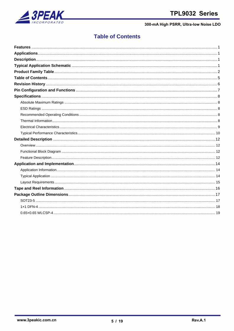
Table of Contents
Features ........................................................................................................................................................................... 1
Applications ..................................................................................................................................................................... 1
Description ....................................................................................................................................................................... 1
Typical Application Schematic ...................................................................................................................................... 1
Product Family Table ...................................................................................................................................................... 2
Table of Contents ............................................................................................................................................................ 5
Revision History .............................................................................................................................................................. 6
Pin Configuration and Functions .................................................................................................................................. 7
Specifications .................................................................................................................................................................. 8
Absolute Maximum Ratings .......................................................................................................................................................... 8
ESD Ratings ................................................................................................................................................................................. 8
Recommended Operating Conditions ........................................................................................................................................... 8
Thermal Information ...................................................................................................................................................................... 8
Electrical Characteristics ............................................................................................................................................................... 9
Typical Performance Characteristics........................................................................................................................................... 10
Detailed Description ..................................................................................................................................................... 12
Overview ..................................................................................................................................................................................... 12
Functional Block Diagram ........................................................................................................................................................... 12
Feature Description ..................................................................................................................................................................... 12
Application and Implementation.................................................................................................................................. 14
Application Information ................................................................................................................................................................ 14
Typical Application ...................................................................................................................................................................... 14
Layout Requirements .................................................................................................................................................................. 15
Tape and Reel Information ........................................................................................................................................... 16
Package Outline Dimensions ....................................................................................................................................... 17
SOT23-5 ..................................................................................................................................................................................... 17
1×1 DFN-4 .................................................................................................................................................................................. 18
0.65×0.65 WLCSP-4 ................................................................................................................................................................... 19
www.3peakic.com.cn Rev.A.1
6 / 19
TPL9032 Series
300-mA High PSRR, Ultra-low Noise LDO
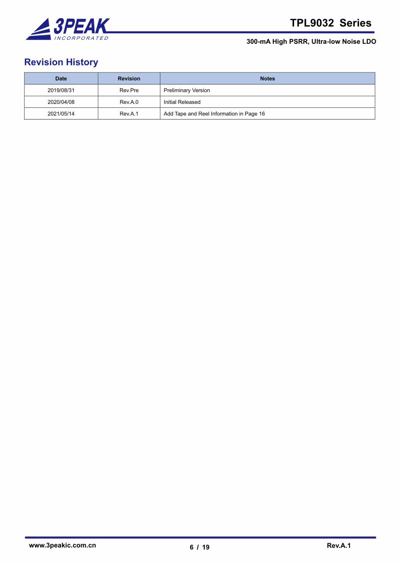
Revision History
Date Revision Notes
2019/08/31 Rev.Pre Preliminary Version
2020/04/08 Rev.A.0 Initial Released
2021/05/14 Rev.A.1 Add Tape and Reel Information in Page 16
www.3peakic.com.cn Rev.A.1
7 / 19
TPL9032 Series
300-mA High PSRR, Ultra-low Noise LDO
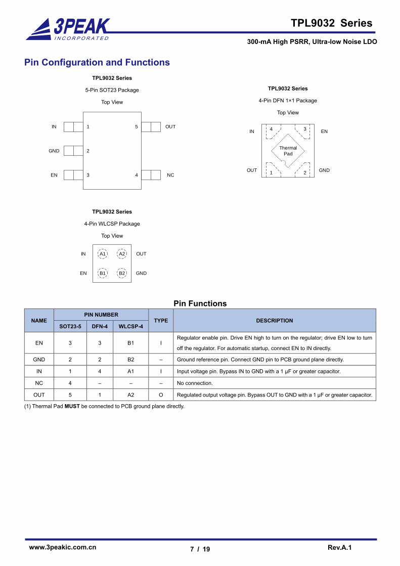
Pin Configuration and Functions
TPL9032 Series
5-Pin SOT23 Package
Top View
1
2
3 4
5IN
GND
EN
OUT
NC
TPL9032 Series
4-Pin DFN 1×1 Package
Top View
1 2
34
OUT GND
ENIN
Thermal
Pad
TPL9032 Series
4-Pin WLCSP Package
Top View
OUT
GNDEN
IN A1 A2
B1 B2
Pin Functions
NAME PIN NUMBER
TYPE DESCRIPTION SOT23-5 DFN-4 WLCSP-4
EN 3 3 B1 I Regulator enable pin. Drive EN high to turn on the regulator; drive EN low to turn
off the regulator. For automatic startup, connect EN to IN directly.
GND 2 2 B2 – Ground reference pin. Connect GND pin to PCB ground plane directly.
IN 1 4 A1 I Input voltage pin. Bypass IN to GND with a 1 μF or greater capacitor.
NC 4 – – – No connection.
OUT 5 1 A2 O Regulated output voltage pin. Bypass OUT to GND with a 1 μF or greater capacitor.
(1) Thermal Pad MUST be connected to PCB ground plane directly.
www.3peakic.com.cn Rev.A.1
8 / 19
TPL9032 Series
300-mA High PSRR, Ultra-low Noise LDO
Specifications
Absolute Maximum Ratings
MIN MAX UNIT
IN, EN –0.3 6 V
OUT –0.3 6 V
TJ Junction Temperature Range –40 150 °C
TSTG Storage Temperature Range –65 150 °C
TL Lead Temperature (Soldering 10 sec) 260 °C
(1) Stresses beyond the Absolute Maximum Ratings may permanently damage the device.
(2) All voltage values are with respect to GND.
ESD Ratings
Condition Minimum Level UNIT
HBM Human Body Model ESD ANSI/ESDA/JEDEC JS-001 ±6000 V
CDM Charged Device Model ESD ANSI/ESDA/JEDEC JS-002 ±1500 V
Recommended Operating Conditions
MIN MAX UNIT
IN 1.75 5.5 V
EN 0 VIN V
OUT 0 5.5 V
COUT 1 10 µF
ESR of COUT 0.001 0.1 Ω
TJ Junction Temperature Range –40 125 °C
PD Power Dissipation 0 400 mW
Thermal Information
PACKAGE θJA θJC UNIT
SOT23-5 280 62 °C/W
1×1 DFN-4 210 110 °C/W
0.65×0.65 WLCSP-4 TBD TBD °C/W

www.3peakic.com.cn Rev.A.1
9 / 19
TPL9032 Series
300-mA High PSRR, Ultra-low Noise LDO
Electrical Characteristics
All test condition: VIN = VOUT(NOM) + 1V, IOUT = 1 mA, CIN = 1 µF, COUT = 1 µF, –40°C ≤ TJ ≤ +125°C, unless otherwise noted.
PARAMETER TEST CONDITIONS MIN TYP MAX UNIT
Supply Input Voltage and Current
VIN Input supply voltage range 1.75 5.5 V
IGND Ground pin current IOUT = 0 mA 120 µA
ISHDN Shutdown current EN = GND 0.02 2 µA
Enable Input Voltage and Current
VIH(EN) EN logic-input high level (enable) 1.2 VIN V
VIL(EN) EN logic-input low level (disable) 0 0.4 V
IEN EN pin leakage current VEN = 5 V 1 2 µA
Regulated Output Voltage and Current
VOUT Output voltage accuracy –40°C ≤ TJ ≤ +125°C –2% 2%
ΔVOUT Line regulation VIN = VOUT(NOM) + 1 V to 5.5 V 1 mV
Load regulation VIN = VOUT(NOM) + 1 V, IOUT = 1 mA to 300 mA 5 mV
VDO (1) Dropout voltage
VOUT = 3.3V, IOUT = 100mA 28 mV
VOUT = 3.3V, IOUT = 300mA 80 180 mV
IOUT Output voltage VOUT in regulation 0 300 mA
ICL Output current limit VOUT = 0.9 × VOUT(NOM) 500 800 mA
ISC Short-circuit current limit RLOAD = 20 mΩ, TA = 25°C 100 mA
RDIS Active output discharge resistance VEN < VIL(EN) 290 Ω
PSRR Power supply rejection ratio
IOUT = 20 mA, f = 100 Hz 82.1 dB
IOUT = 20 mA, f = 1 kHz 81.9 dB
IOUT = 20 mA, f = 10 kHz 87.9 dB
IOUT = 20 mA, f = 100 kHz 61.4 dB
IOUT = 20 mA, f = 1 MHz 44.7 dB
VN Output noise voltage IOUT = 150 mA, BW = 10Hz to 100 kHz 8.6 μVRMS
tSTR Start-up time VOUT reaches 95% of nominal output voltage
after EN = high 750 μs
Temperature Range
TSD
Thermal shutdown temperature 165 ºC
Thermal shutdown hysteresis 15 ºC
(1) Dropout voltage is the minimum input to output voltage differential needed to maintain regulation at a specified output current and measure for
VOUT(NOM) ≥ 1.8V. In dropout, the output voltage will be equal to: VIN – VDROPOUT.
www.3peakic.com.cn Rev.A.1
10 / 19
TPL9032 Series
300-mA High PSRR, Ultra-low Noise LDO
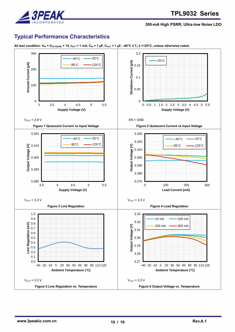
Typical Performance Characteristics
All test condition: VIN = VOUT(NOM) + 1V, IOUT = 1 mA, CIN = 1 µF, COUT = 1 µF, –40°C ≤ TJ ≤ +125°C, unless otherwise noted.
VOUT = 2.8 V
Figure 1 Quiescent Current vs Input Voltage
EN = GND
Figure 2 Quiescent Current vs Input Voltage
VOUT = 3.3 V
Figure 3 Line Regulation
VOUT = 3.3 V
Figure 4 Load Regulation
VOUT = 3.3 V
Figure 5 Line Regulation vs. Temperature
VOUT = 3.3 V
Figure 6 Output Voltage vs. Temperature
0
100
200
300
3 3.5 4 4.5 5 5.5
Gro
un
d C
urr
en
t (µ
A)
Supply Voltage (V)
–40°C 25°C
85°C 125°C
0
0.05
0.1
0.15
0.2
0 0.5 1 1.5 2 2.5 3 3.5 4 4.5 5 5.5
Sh
utd
ow
n C
urr
en
t (µ
A)
Supply Voltage (V)
25°C
3.280
3.290
3.300
3.310
3.320
3.5 4 4.5 5 5.5
Ou
tpu
t V
olt
ag
e (
V)
Supply Voltage (V)
–40°C 25°C
85°C 125°C
3.270
3.280
3.290
3.300
3.310
3.320
3.330
0 100 200 300
Ou
tpu
t V
olt
ag
e (
V)
Load Current (mA)
–40°C 25°C
85°C 125°C
0.0
0.1
0.2
0.3
0.4
0.5
0.6
0.7
0.8
0.9
1.0
-40 -25 -10 5 20 35 50 65 80 95 110 125
Lin
e R
eg
ula
tio
n (
mV
)
Ambient Temperature (°C)
3.27
3.28
3.29
3.30
3.31
3.32
3.33
-40 -25 -10 5 20 35 50 65 80 95 110 125
Ou
tpu
t V
olt
ag
e (
V)
Ambient Temperature (°C)
10 mA 100 mA
200 mA 300 mA
www.3peakic.com.cn Rev.A.1
11 / 19
TPL9032 Series
300-mA High PSRR, Ultra-low Noise LDO
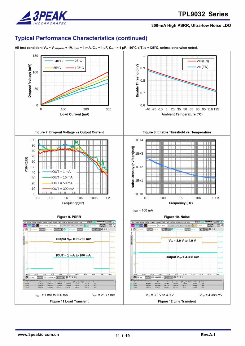
Typical Performance Characteristics (continued)
All test condition: VIN = VOUT(NOM) + 1V, IOUT = 1 mA, CIN = 1 µF, COUT = 1 µF, –40°C ≤ TJ ≤ +125°C, unless otherwise noted.
Figure 7. Dropout Voltage vs Output Current
Figure 8. Enable Threshold vs. Temperature
Figure 9. PSRR
IOUT = 100 mA
Figure 10. Noise
IOUT = 1 mA to 100 mA
Output VPP = 21.766 mV
IOUT = 1 mA to 100 mA VPP = 21.77 mV
Figure 11 Load Transient
Output VPP = 4.388 mV
VIN = 3.9 V to 4.9 V
VIN = 3.9 V to 4.9 V VPP = 4.388 mV
Figure 12 Line Transient
0
50
100
150
0 100 200 300
Dro
po
ut
Vo
ltag
e (
mV
)
Load Current (mA)
−40°C 25°C
85°C 125°C
0.6
0.7
0.8
0.9
1
-40 -25 -10 5 20 35 50 65 80 95 110 125
En
ab
le T
hre
sh
old
(V
)
Ambient Temperature (°C)
VIH(EN)
VIL(EN)
0
10
20
30
40
50
60
70
80
90
100
10 100 1K 10K 100K 1M
PS
RR
(dB
)
Frequency(Hz)
IOUT = 1 mA
IOUT = 10 mA
IOUT = 50 mA
IOUT = 300 mA
1E+0
1E+1
1E+2
1E+3
1E+4
10 100 1K 10K 100K
No
ise D
en
sit
y (
nV
/sq
rt(H
z))
Frequency (Hz)
www.3peakic.com.cn Rev.A.1
12 / 19
TPL9032 Series
300-mA High PSRR, Ultra-low Noise LDO
Detailed Description
Overview
The TPL9032 series products are 300-mA high PSRR, ultra-low noise, low dropout linear regulators with high output accuracy. The
TPL9032 series products support both fixed output voltage ranges from 0.9 V to 5 V is stable with 1 μF or larger ceramic output
capacitor.
The TPL9032 series products have high PSRR with 87.9 dB at 10 kHz and 8.6 μVRMS ultra-low noise. These features make TPL9032
series products very suitable for noise-sensitive applications with high noise from previous stage power supply, such as high-
performance analog devices, or high-definition imaging equipment. Output shortage protection and thermal overload protection
circuits improves the reliability under heavy load conditions.
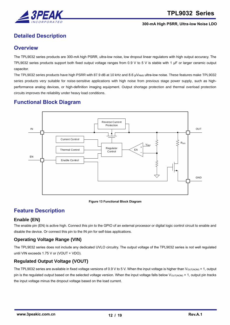
Functional Block Diagram
IN
GND
Regulator
Control
Current Control
Thermal Control
Enable Contro l
+
–EA
EN
OUT
VREF
RDIS
Reverse Current
Protection
Figure 13 Functional Block Diagram
Feature Description
Enable (EN)
The enable pin (EN) is active high. Connect this pin to the GPIO of an external processor or digital logic control circuit to enable and
disable the device. Or connect this pin to the IN pin for self-bias applications.
Operating Voltage Range (VIN)
The TPL9032 series does not include any dedicated UVLO circuitry. The output voltage of the TPL9032 series is not well regulated
until VIN exceeds 1.75 V or (VOUT + VDO).
Regulated Output Voltage (VOUT)
The TPL9032 series are available in fixed voltage versions of 0.9 V to 5 V. When the input voltage is higher than VOUT(NOM) + 1, output
pin is the regulated output based on the selected voltage version. When the input voltage falls below VOUT(NOM) + 1, output pin tracks
the input voltage minus the dropout voltage based on the load current.
www.3peakic.com.cn Rev.A.1
13 / 19
TPL9032 Series
300-mA High PSRR, Ultra-low Noise LDO
Reverse-Current Protection (RCP)
The TPL9032 series provide the reverse-current protection (RCP) to prevent output reverse current. If large capacitors been used at
the output, there would be large reverse current when the input voltage is lower than output voltage. The TPL9032 series can shut
off the regulator and body diode path to prevent the device damaged from reverse current fault.
Current Limit
The TPL9032 series integrate an internal current limit that helps to protect the regulator during fault conditions. When the output is
shorted, the LDO supplies a typical current of 100 mA. Output voltage is not regulated when the device is in current limit, and VOUT =
ICL × RLOAD.
Thermal Shutdown
During normal operation, LDO junction temperature should not exceed 125°C. When the junction temperature exceeds the thermal
shutdown threshold, the LDO shut down the output immediately. Until when the junction temperature falls below the thermal shutdown
threshold minus thermal shutdown hysteresis, the output turns on again.
www.3peakic.com.cn Rev.A.1
14 / 19
TPL9032 Series
300-mA High PSRR, Ultra-low Noise LDO
Application and Implementation
Application Information
The TPL9032 devices are a series of 300-mA high PSRR, ultra-low noise, low-dropout linear regulator. The following application
schematic shows a typical usage of the TPL9032 series.
Typical Application
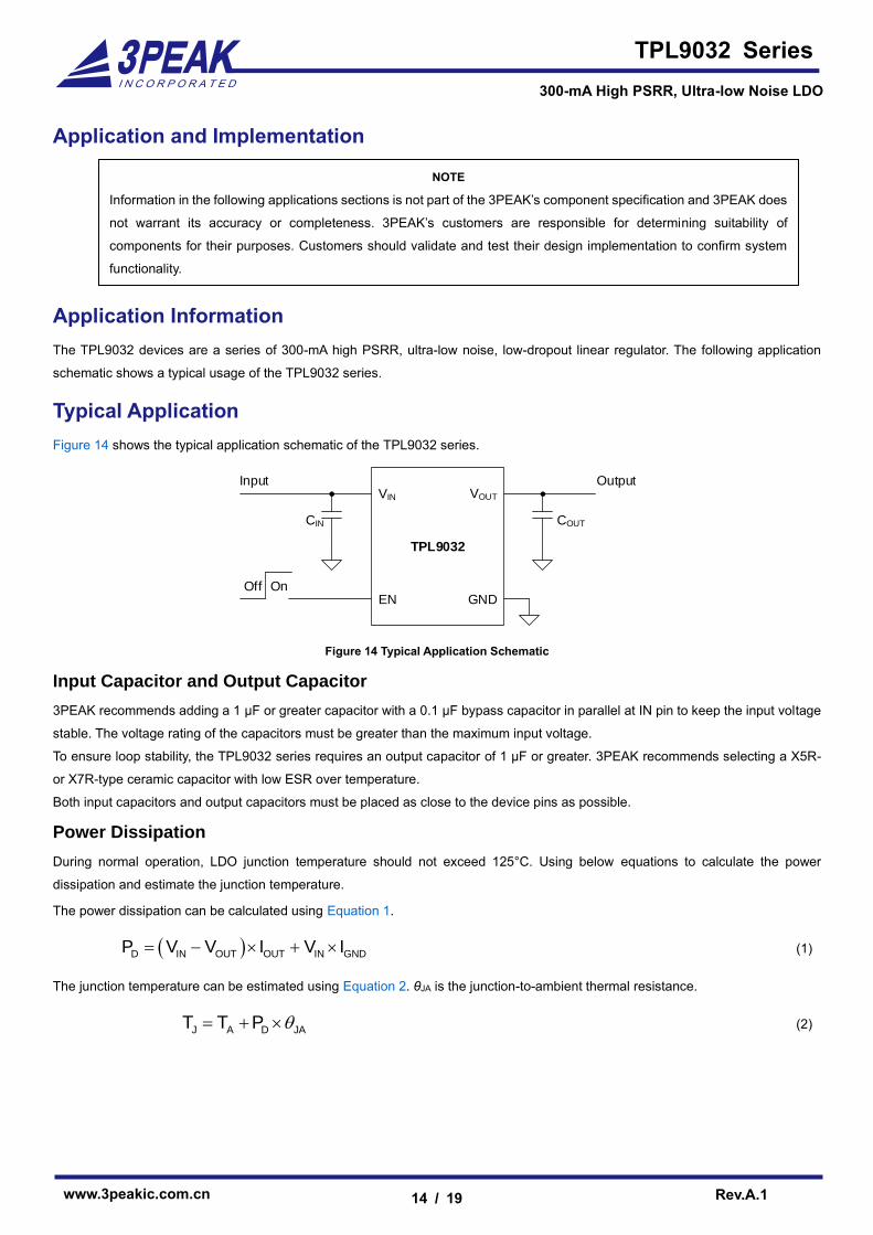
Figure 14 shows the typical application schematic of the TPL9032 series.
VIN VOUT
EN GND
Input
Off On
TPL9032
COUT
Output
CIN
Figure 14 Typical Application Schematic
Input Capacitor and Output Capacitor
3PEAK recommends adding a 1 μF or greater capacitor with a 0.1 μF bypass capacitor in parallel at IN pin to keep the input voltage
stable. The voltage rating of the capacitors must be greater than the maximum input voltage.
To ensure loop stability, the TPL9032 series requires an output capacitor of 1 μF or greater. 3PEAK recommends selecting a X5R-
or X7R-type ceramic capacitor with low ESR over temperature.
Both input capacitors and output capacitors must be placed as close to the device pins as possible.
Power Dissipation
During normal operation, LDO junction temperature should not exceed 125°C. Using below equations to calculate the power
dissipation and estimate the junction temperature.
The power dissipation can be calculated using Equation 1.
( )D IN OUT OUT IN GNDP V V I V I= − + (1)
The junction temperature can be estimated using Equation 2. θJA is the junction-to-ambient thermal resistance.
J A D JAT T P = + (2)
NOTE
Information in the following applications sections is not part of the 3PEAK’s component specification and 3PEAK does
not warrant its accuracy or completeness. 3PEAK’s customers are responsible for determining suitability of
components for their purposes. Customers should validate and test their design implementation to confirm system
functionality.
www.3peakic.com.cn Rev.A.1
15 / 19
TPL9032 Series
300-mA High PSRR, Ultra-low Noise LDO
Layout Requirements
• Both input capacitors and output capacitors must be placed as close to the device pins as possible.
• It is recommended to bypass the input pin to ground with a 0.1 μF bypass capacitor. The loop area formed by the bypass
capacitor connection, IN pin and the GND pin of the system must be as small as possible.
• It is recommended to use wide trace lengths or thick copper weight to minimize I×R drop and heat dissipation.
www.3peakic.com.cn Rev.A.1
16 / 19
TPL9032 Series
300-mA High PSRR, Ultra-low Noise LDO
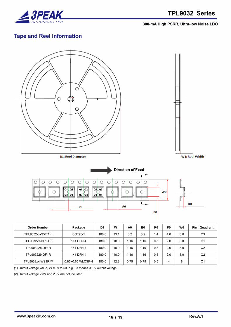
Tape and Reel Information
Order Number Package D1 W1 A0 B0 K0 P0 W0 Pin1 Quadrant
TPL9032xx-S5TR (1) SOT23-5 180.0 13.1 3.2 3.2 1.4 4.0 8.0 Q3
TPL9032xx-DF1R (2) 1×1 DFN-4 180.0 10.0 1.16 1.16 0.5 2.0 8.0 Q1
TPL903228-DF1R 1×1 DFN-4 180.0 10.0 1.16 1.16 0.5 2.0 8.0 Q2
TPL903229-DF1R 1×1 DFN-4 180.0 10.0 1.16 1.16 0.5 2.0 8.0 Q2
TPL9032xx-WS1R (1) 0.65×0.65 WLCSP-4 180.0 12.3 0.75 0.75 0.5 4 8 Q1
(1) Output voltage value, xx = 09 to 50. e.g. 33 means 3.3 V output voltage.
(2) Output voltage 2.8V and 2.9V are not included.
www.3peakic.com.cn Rev.A.1
17 / 19
TPL9032 Series
300-mA High PSRR, Ultra-low Noise LDO
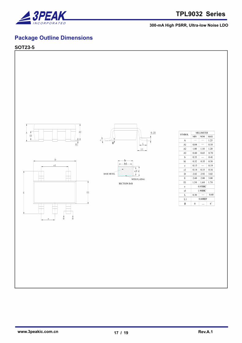
Package Outline Dimensions
SOT23-5
www.3peakic.com.cn Rev.A.1
18 / 19
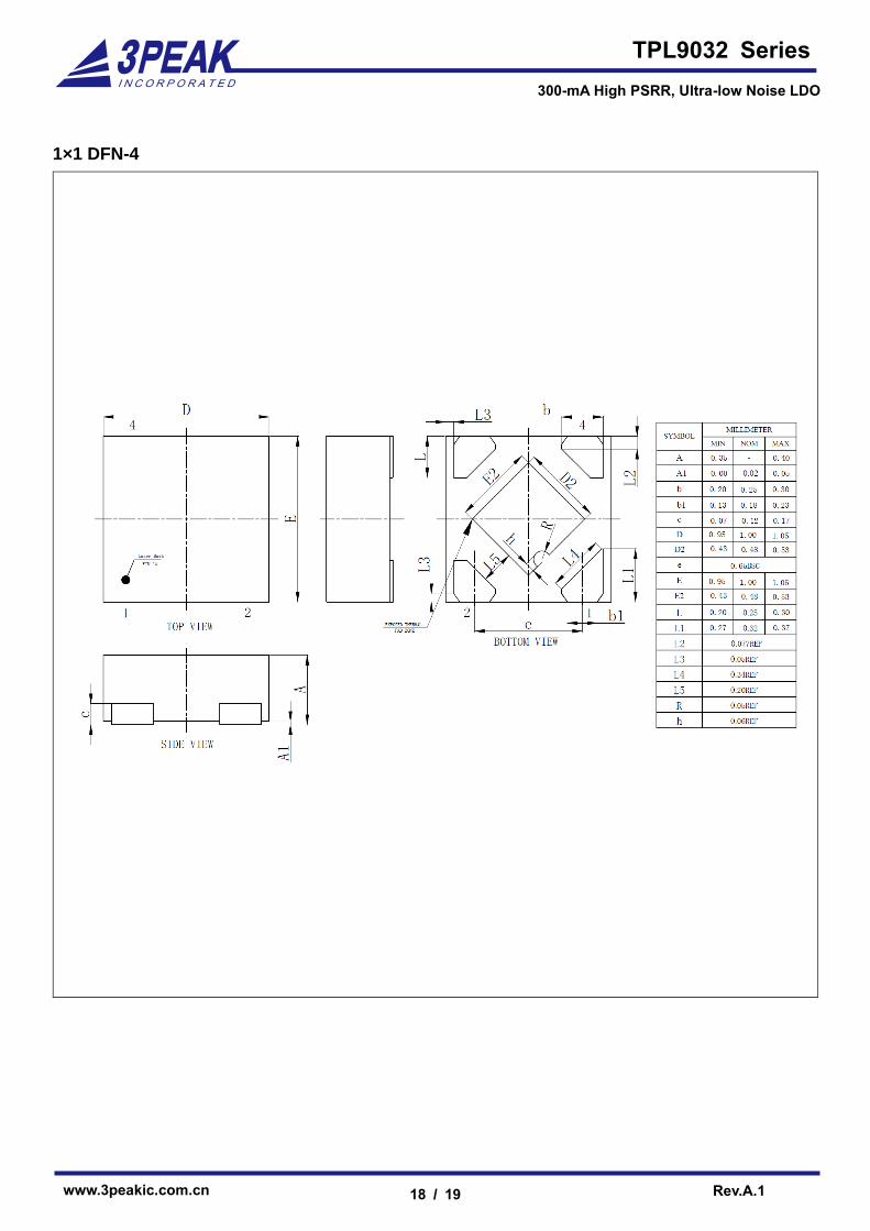
TPL9032 Series
300-mA High PSRR, Ultra-low Noise LDO
1×1 DFN-4
www.3peakic.com.cn Rev.A.1
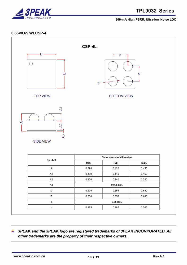
19 / 19
TPL9032 Series
300-mA High PSRR, Ultra-low Noise LDO
0.65×0.65 WLCSP-4
Symbol Dimensions in Millimeters
Min. Typ. Max.
A 0.390 0.420 0.450
A1 0.130 0.145 0.160
A2 0.230 0.240 0.250
A3 0.025 Ref.
D 0.630 0.655 0.680
E 0.630 0.655 0.680
e 0.35 BSC
b 0.165 0.185 0.205
3PEAK and the 3PEAK logo are registered trademarks of 3PEAK INCORPORATED. All
other trademarks are the property of their respective owners.