
TP07 3 P E A K - · PDF file3 P E A K 1 TP07 Precision RRO Operational Amplifier
9
3PEAK 1 TP07 Precision RRO Operational Amplifier www.3peakic.com REV0.0 Features Low Offset Voltage: 100μV Maximum Low Drift: ±0.9μV/°C High EMIRR: 84dB at 900MHz Low Noise: 19 nV/√Hz(f= 1kHz) Wide Input Voltage Range: 0 to ±14V Wide Supply Range: ±1.35V to ±18V Low Input Bias Current: 40pA Typical Below-Ground (V-) Input Capability to -0.3V Rail-to-Rail Output Voltage Range Unit Gain Stable –40°C to 125°C Operation Range Robust 3kV – HBM and 2kV – CDM ESD Rating Direct or Update Replacement for OP07C,OP07D and OP37 Applications Wireless Base Station Control Circuits Optical network Control Circuits I/V Converter Temperature Measurements Strain Gage Amplifier Medical Instrumentation Pin Configuration (Top View) TP07 8-Pin SOIC (-S Suffix) 8 6 5 7 3 2 1 4 NC ﹢In ﹣In Out ﹣Vs ﹢Vs NC NC Description The TP07 has very low input offset voltage (100μV maximum) that is obtained by trimming at the wafer stage. The low offset voltages generally eliminate any need for external nulling. The TP07 also features low input bias current (±40 pA) and high open-loop gain (118 dB). The low offset and high open-loop gain make the TP07 particularly useful for high gain instrumentation applications. The wide input voltage range of ± 14 V minimum combined with a high CMRR of 126 dB and high input impedance provide high accuracy in the non-inverting circuit configuration. Excellent linearity and gain accuracy can be maintained even at high closed-loop gains. Stability of offsets and gain with time or variations in temperature is excellent. The accuracy and stability of the TP07, even at high gain, made the TP07 an industry standard for instrumentation applications. The TP07 is single channel available in 8-pin SOIC package. 3PEAK and the 3PEAK logo are registered trademarks of 3PEAK INCORPORATED. All other trademarks are the property of their respective owners. Order Information Model Name Order Number Package Transport Media, Quantity Marking Information TP07 TP07-SR 8-Pin SOIC Tape and Reel, 4,000 D41S TP07
Transcript of TP07 3 P E A K - · PDF file3 P E A K 1 TP07 Precision RRO Operational Amplifier
3PEAK
1
TP07
Precision RRO Operational Amplifier
www.3peakic.com REV0.0
Features
Low Offset Voltage: 100μV Maximum
Low Drift: ±0.9μV/°C
High EMIRR: 84dB at 900MHz
Low Noise: 19 nV/√Hz(f= 1kHz)
Wide Input Voltage Range: 0 to ±14V
Wide Supply Range: ±1.35V to ±18V
Low Input Bias Current: 40pA Typical
Below-Ground (V-) Input Capability to -0.3V
Rail-to-Rail Output Voltage Range
Unit Gain Stable
–40°C to 125°C Operation Range
Robust 3kV – HBM and 2kV – CDM ESD Rating
Direct or Update Replacement for OP07C,OP07D
and OP37
Applications
Wireless Base Station Control Circuits
Optical network Control Circuits
I/V Converter
Temperature Measurements
Strain Gage Amplifier
Medical Instrumentation
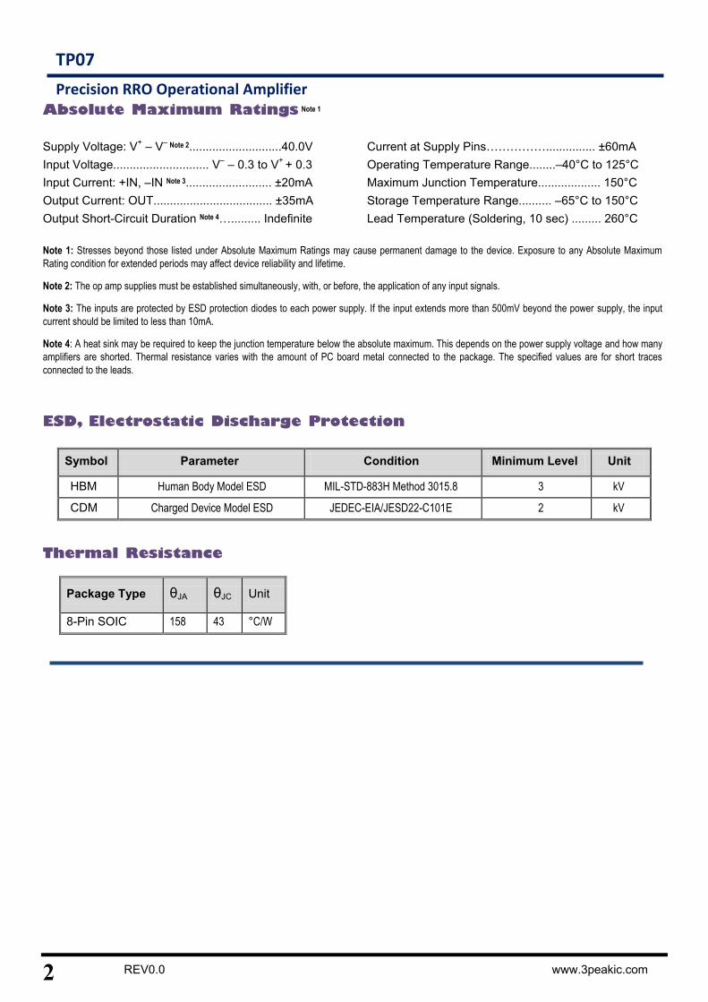
Pin Configuration (Top View)
TP07
8-Pin SOIC
(-S Suffix)
8
6
5
7
3
2
1
4
NC
﹢In
﹣In
Out
﹣Vs
﹢Vs
NC
NC
Description
The TP07 has very low input offset voltage (100μV
maximum) that is obtained by trimming at the wafer
stage. The low offset voltages generally eliminate any
need for external nulling. The TP07 also features low
input bias current (±40 pA) and high open-loop gain
(118 dB). The low offset and high open-loop gain make
the TP07 particularly useful for high gain
instrumentation applications.
The wide input voltage range of ±14 V minimum
combined with a high CMRR of 126 dB and high input
impedance provide high accuracy in the non-inverting
circuit configuration. Excellent linearity and gain
accuracy can be maintained even at high closed-loop
gains. Stability of offsets and gain with time or
variations in temperature is excellent. The accuracy
and stability of the TP07, even at high gain, made the
TP07 an industry standard for instrumentation
applications.
The TP07 is single channel available in 8-pin SOIC
package.
3PEAK and the 3PEAK logo are registered trademarks of
3PEAK INCORPORATED. All other trademarks are the property of
their respective owners.
Order Information
Model Name Order Number Package Transport Media, Quantity Marking
Information
TP07 TP07-SR 8-Pin SOIC Tape and Reel, 4,000 D41S
TP07
2 REV0.0 www.3peakic.com
TP07
Precision RRO Operational Amplifier
Absolute Maximum Ratings Note 1
Supply Voltage: V+ – V
– Note 2............................40.0V
Input Voltage............................. V– – 0.3 to V
+ + 0.3
Input Current: +IN, –IN Note 3.......................... ±20mA
Output Current: OUT.................................... ±35mA
Output Short-Circuit Duration Note 4…......... Indefinite
Current at Supply Pins……………............... ±60mA
Operating Temperature Range........–40°C to 125°C
Maximum Junction Temperature................... 150°C
Storage Temperature Range.......... –65°C to 150°C
Lead Temperature (Soldering, 10 sec) ......... 260°C
Note 1: Stresses beyond those listed under Absolute Maximum Ratings may cause permanent damage to the device. Exposure to any Absolute Maximum
Rating condition for extended periods may affect device reliability and lifetime.
Note 2: The op amp supplies must be established simultaneously, with, or before, the application of any input signals.
Note 3: The inputs are protected by ESD protection diodes to each power supply. If the input extends more than 500mV beyond the power supply, the input
current should be limited to less than 10mA.
Note 4: A heat sink may be required to keep the junction temperature below the absolute maximum. This depends on the power supply voltage and how many
amplifiers are shorted. Thermal resistance varies with the amount of PC board metal connected to the package. The specified values are for short traces
connected to the leads.
ESD, Electrostatic Discharge Protection
Symbol Parameter Condition Minimum Level Unit
HBM Human Body Model ESD MIL-STD-883H Method 3015.8 3 kV
CDM Charged Device Model ESD JEDEC-EIA/JESD22-C101E 2 kV
Thermal Resistance
Package Type θJA θJC Unit
8-Pin SOIC 158 43 ° C/W
3
TP07
Precision RRO Operational Amplifier
www.3peakic.com REV0.0
Electrical Characteristics
The specifications are at TA = 27° C, VSUPPLY = ±15V, VCM = VOUT =0V, RL = 2kΩ, CL =100pF. Unless otherwise noted.
SYMBOL PARAMETER CONDITIONS MIN TYP MAX UNITS
VOS Input Offset Voltage VCM = VDD/2 -100 ± 50 +100 μV
VOS TC Input Offset Voltage Drift -40° C to 125° C 0.9 μV/° C
IB Input Bias Current
TA = 27 ° C 40 pA
TA = 85 ° C 550 pA
TA = 125 ° C 7.7 nA
IOS Input Offset Current 0.001 pA
Vn Input Voltage Noise f = 0.1Hz to 10Hz 2.35 μVRMS
en Input Voltage Noise Density f = 1kHz 19 nV/√Hz
CIN Input Capacitance Differential
Common Mode
4
2.5 pF
CMRR Common Mode Rejection Ratio VCM = -5.6V to 4V 120 dB
VCM Common-mode Input Voltage
Range V– -0.3 V+-2.0 V
PSRR Power Supply Rejection Ratio 130 dB
AVOL Open-Loop Large Signal Gain RLOAD = 2kΩ 100 118 dB
VOL, VOH Output Swing from Supply Rail RLOAD = 100kΩ 50 mV
ROUT Closed-Loop Output Impedance G = 1, f =1kHz, IOUT = 0 0.01 Ω
RO Open-Loop Output Impedance f = 1kHz, IOUT = 0 125 Ω
ISC Output Short-Circuit Current Sink or source current 35 mA
VDD Supply Voltage 2.7 36 V
IQ Quiescent Current per Amplifier 2.2 mA
PM Phase Margin RLOAD = 2kΩ, CLOAD = 100pF 55 °
GM Gain Margin RLOAD = 2kΩ, CLOAD = 100pF 8 dB
GBWP Gain-Bandwidth Product f = 1kHz 1 MHz
SR Slew Rate AV = 1, VOUT = 0V to 10V, CLOAD = 100pF,
RLOAD = 2kΩ 6 V/μs
FPBW Full Power Bandwidth Note 1 210 kHz
tS Settling Time, 0.1%
Settling Time, 0.01% AV = –1, 10V Step
1
1 μs
Xtalk Channel Separation f = 1kHz, RL = 2kΩ 110 dB
Note 1: Full power bandwidth is calculated from the slew rate FPBW = SR/π • VP-P
4 REV0.0 www.3peakic.com
TP07
Precision RRO Operational Amplifier
Typical Performance Characteristics
VS = ±15V, VCM = 0V, RL = Open, unless otherwise specified.
Offset Voltage Production Distribution Offset Voltage vs. Temperature
0
2
4
6
8
10
12
14
16
18
Po
pu
lati
on
Offset Voltage(μV)
-40
-20
0
20
40
60
80
100
120
-60 -40 -20 0 20 40 60 80 100 120 140
Off
se
t V
olt
ag
e (
μV
)
Temperature (℃)
Input Voltage Noise Spectral Density Input Bias Current vs. Temperature
1
10
100
1k
0.1 1 10 100 1k 10k 100k 1M
No
ise (n
V/√
Hz)
Frequency (Hz)
VDD=30VRL=1kΩ
1E-18
1E-16
1E-14
1E-12
1E-10
1E-08
-50 0 50 100
Inp
ut B
ias C
urr
en
t (A
)
Temperature (C)
Common Mode Rejection Ratio Quiescent Current vs. Temperature
50
100
150
-15 -12 -9 -6 -3 0 3 6 9 12 15
CM
RR
(dB
)
Common Mode Voltage (V)
0
0 . 2
0 . 4
0 . 6
0 . 8
1
1 . 2
1 . 4
-50 0 50 100 150
Su
pp
ly
C
ur
re
nt
(
mA
)
T e m p e r a t u r e (℃)
5
TP07
Precision RRO Operational Amplifier
www.3peakic.com REV0.0
Typical Performance Characteristics
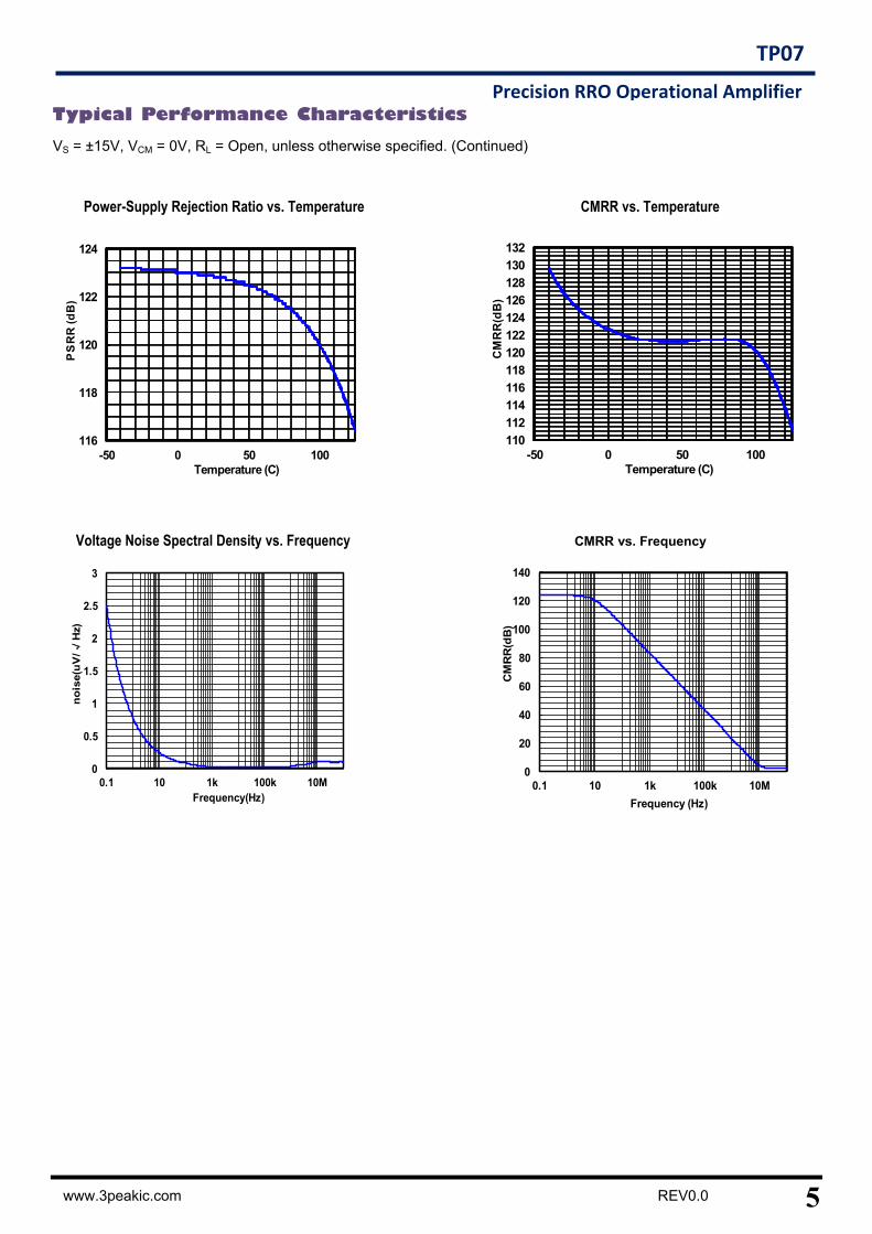
VS = ±15V, VCM = 0V, RL = Open, unless otherwise specified. (Continued)
Power-Supply Rejection Ratio vs. Temperature CMRR vs. Temperature
116
118
120
122
124
-50 0 50 100
PS
RR
(d
B)
Temperature (C)
110
112
114
116
118
120
122
124
126
128
130
132
-50 0 50 100
CM
RR
(dB
)
Temperature (C)
Voltage Noise Spectral Density vs. Frequency CMRR vs. Frequency
0
0.5
1
1.5
2
2.5
3
0.1 10 1k 100k 10M
no
ise(u
V/√
Hz)
Frequency(Hz)
0
20
40
60
80
100
120
140
0.1 10 1k 100k 10M
CM
RR
(dB
)
Frequency (Hz)
6 REV0.0 www.3peakic.com
TP07
Precision RRO Operational Amplifier
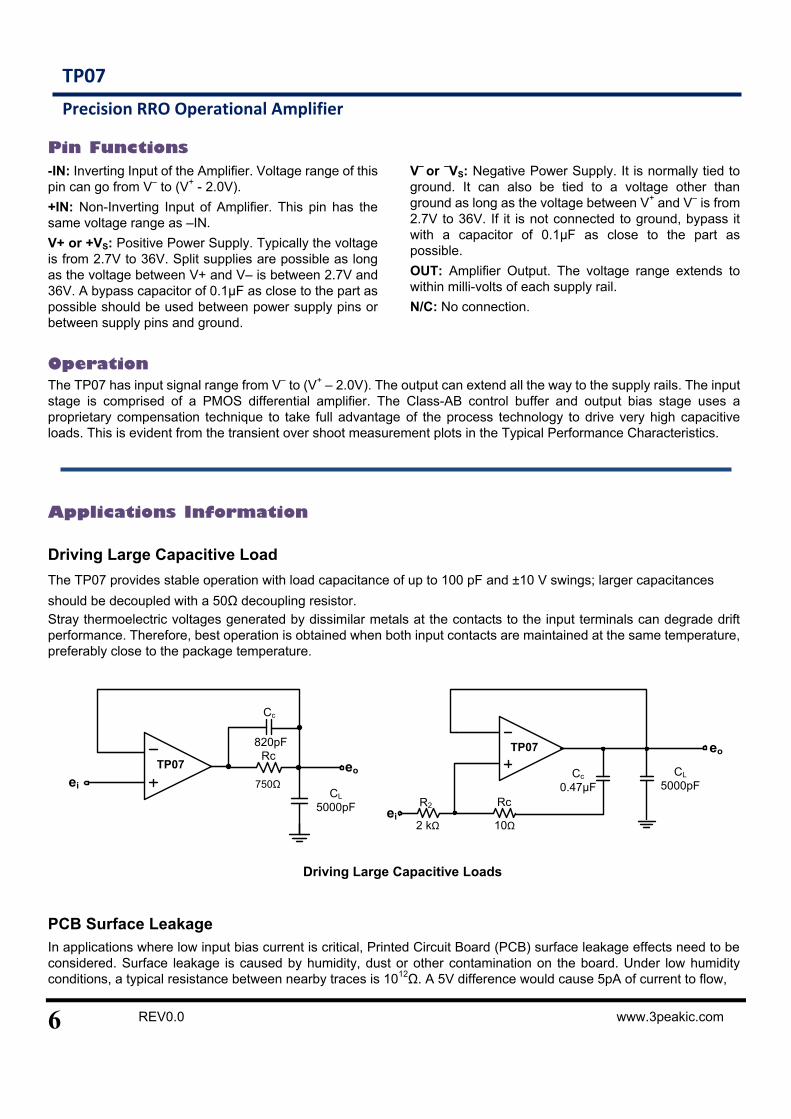
Pin Functions
-IN: Inverting Input of the Amplifier. Voltage range of this
pin can go from V– to (V
+ - 2.0V).
+IN: Non-Inverting Input of Amplifier. This pin has the
same voltage range as –IN.
V+ or +VS: Positive Power Supply. Typically the voltage
is from 2.7V to 36V. Split supplies are possible as long
as the voltage between V+ and V– is between 2.7V and
36V. A bypass capacitor of 0.1μF as close to the part as
possible should be used between power supply pins or
between supply pins and ground.
V– or
–VS: Negative Power Supply. It is normally tied to
ground. It can also be tied to a voltage other than
ground as long as the voltage between V+ and V
– is from
2.7V to 36V. If it is not connected to ground, bypass it
with a capacitor of 0.1μF as close to the part as
possible.
OUT: Amplifier Output. The voltage range extends to
within milli-volts of each supply rail.
N/C: No connection.
Operation
The TP07 has input signal range from V– to (V
+ – 2.0V). The output can extend all the way to the supply rails. The input
stage is comprised of a PMOS differential amplifier. The Class-AB control buffer and output bias stage uses a
proprietary compensation technique to take full advantage of the process technology to drive very high capacitive
loads. This is evident from the transient over shoot measurement plots in the Typical Performance Characteristics.
Applications Information
Driving Large Capacitive Load
The TP07 provides stable operation with load capacitance of up to 100 pF and ±10 V swings; larger capacitances
should be decoupled with a 50Ω decoupling resistor.
Stray thermoelectric voltages generated by dissimilar metals at the contacts to the input terminals can degrade drift
performance. Therefore, best operation is obtained when both input contacts are maintained at the same temperature,
preferably close to the package temperature.
TP07
ei
820pF
Cc
eo
CL
5000pF
TP07
ei
eo
CL
5000pFCc
0.47µF
RcR2
10Ω2 kΩ
Rc
750Ω
Driving Large Capacitive Loads
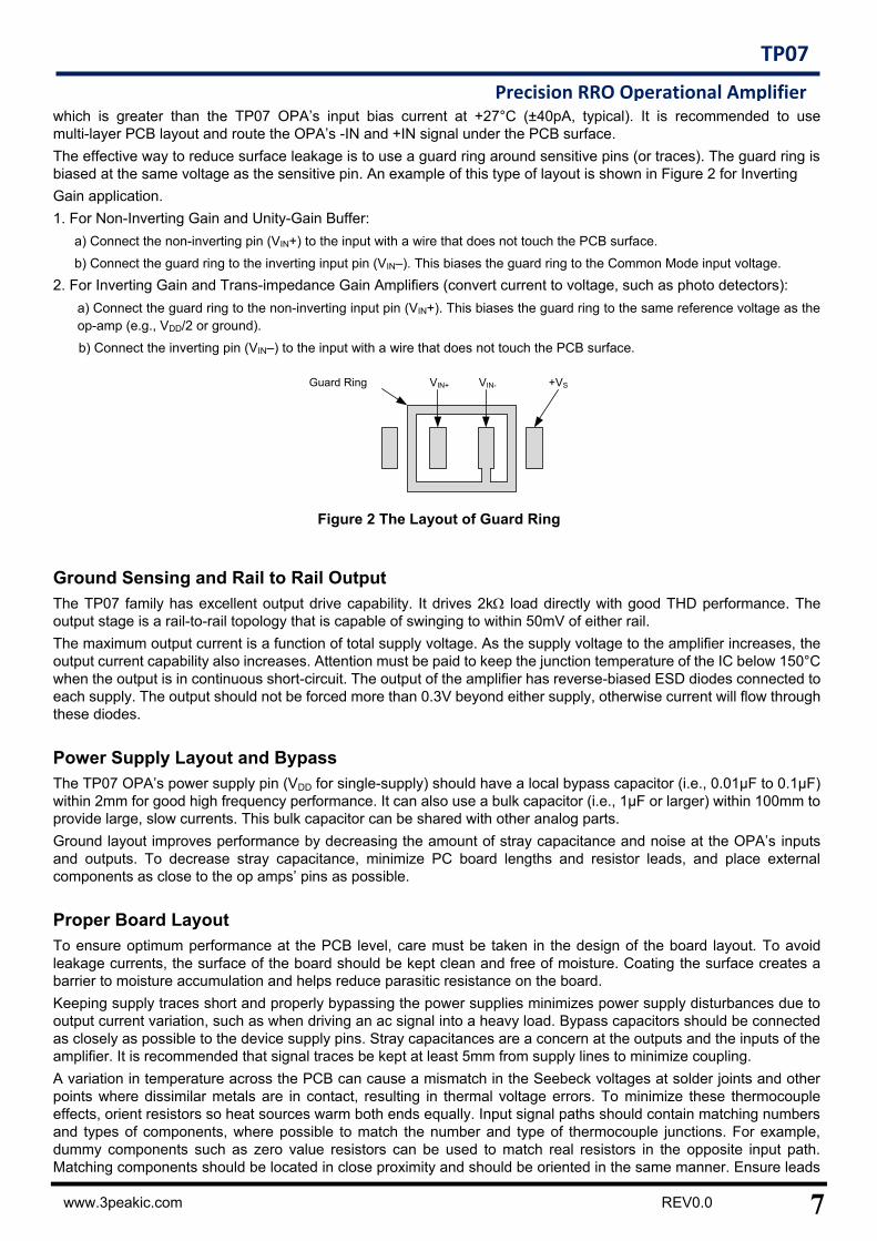
PCB Surface Leakage
In applications where low input bias current is critical, Printed Circuit Board (PCB) surface leakage effects need to be
considered. Surface leakage is caused by humidity, dust or other contamination on the board. Under low humidity
conditions, a typical resistance between nearby traces is 1012
Ω. A 5V difference would cause 5pA of current to flow,
7
TP07
Precision RRO Operational Amplifier
www.3peakic.com REV0.0
which is greater than the TP07 OPA’s input bias current at +27°C (±40pA, typical). It is recommended to use
multi-layer PCB layout and route the OPA’s -IN and +IN signal under the PCB surface.
The effective way to reduce surface leakage is to use a guard ring around sensitive pins (or traces). The guard ring is
biased at the same voltage as the sensitive pin. An example of this type of layout is shown in Figure 2 for Inverting
Gain application.
1. For Non-Inverting Gain and Unity-Gain Buffer:
a) Connect the non-inverting pin (VIN+) to the input with a wire that does not touch the PCB surface.
b) Connect the guard ring to the inverting input pin (VIN–). This biases the guard ring to the Common Mode input voltage.
2. For Inverting Gain and Trans-impedance Gain Amplifiers (convert current to voltage, such as photo detectors):
a) Connect the guard ring to the non-inverting input pin (VIN+). This biases the guard ring to the same reference voltage as the
op-amp (e.g., VDD/2 or ground).
b) Connect the inverting pin (VIN–) to the input with a wire that does not touch the PCB surface.
VIN+ VIN- +VSGuard Ring
Figure 2 The Layout of Guard Ring
Ground Sensing and Rail to Rail Output
The TP07 family has excellent output drive capability. It drives 2k load directly with good THD performance. The
output stage is a rail-to-rail topology that is capable of swinging to within 50mV of either rail.
The maximum output current is a function of total supply voltage. As the supply voltage to the amplifier increases, the
output current capability also increases. Attention must be paid to keep the junction temperature of the IC below 150°C
when the output is in continuous short-circuit. The output of the amplifier has reverse-biased ESD diodes connected to
each supply. The output should not be forced more than 0.3V beyond either supply, otherwise current will flow through
these diodes.
Power Supply Layout and Bypass
The TP07 OPA’s power supply pin (VDD for single-supply) should have a local bypass capacitor (i.e., 0.01μF to 0.1μF)
within 2mm for good high frequency performance. It can also use a bulk capacitor (i.e., 1μF or larger) within 100mm to
provide large, slow currents. This bulk capacitor can be shared with other analog parts.
Ground layout improves performance by decreasing the amount of stray capacitance and noise at the OPA’s inputs
and outputs. To decrease stray capacitance, minimize PC board lengths and resistor leads, and place external
components as close to the op amps’ pins as possible.
Proper Board Layout
To ensure optimum performance at the PCB level, care must be taken in the design of the board layout. To avoid
leakage currents, the surface of the board should be kept clean and free of moisture. Coating the surface creates a
barrier to moisture accumulation and helps reduce parasitic resistance on the board.
Keeping supply traces short and properly bypassing the power supplies minimizes power supply disturbances due to
output current variation, such as when driving an ac signal into a heavy load. Bypass capacitors should be connected
as closely as possible to the device supply pins. Stray capacitances are a concern at the outputs and the inputs of the
amplifier. It is recommended that signal traces be kept at least 5mm from supply lines to minimize coupling.
A variation in temperature across the PCB can cause a mismatch in the Seebeck voltages at solder joints and other
points where dissimilar metals are in contact, resulting in thermal voltage errors. To minimize these thermocouple
effects, orient resistors so heat sources warm both ends equally. Input signal paths should contain matching numbers
and types of components, where possible to match the number and type of thermocouple junctions. For example,
dummy components such as zero value resistors can be used to match real resistors in the opposite input path.
Matching components should be located in close proximity and should be oriented in the same manner. Ensure leads
8 REV0.0 www.3peakic.com
TP07
Precision RRO Operational Amplifier
are of equal length so that thermal conduction is in equilibrium. Keep heat sources on the PCB as far away from
amplifier input circuitry as is practical.
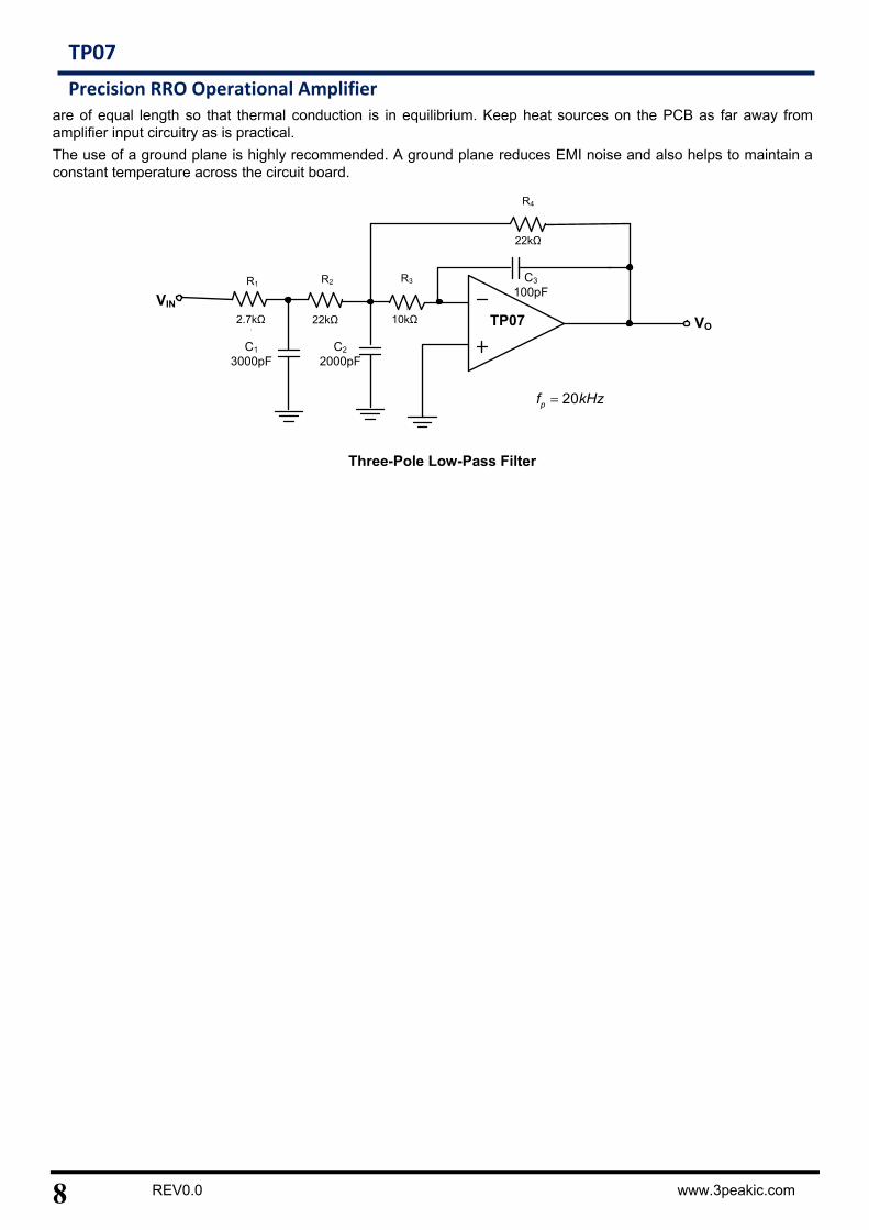
The use of a ground plane is highly recommended. A ground plane reduces EMI noise and also helps to maintain a
constant temperature across the circuit board.
TP07
VIN
C1
3000pF
R2
22kΩ
22kΩ
R4
R1
2.7kΩ 10kΩ
R3 C3
100pF
VO
C2
2000pF
20pf kHz
Three-Pole Low-Pass Filter
9
TP07
Precision RRO Operational Amplifier
www.3peakic.com REV0.0
D
E1
b
E
A1
A2
e
θ
L1
C
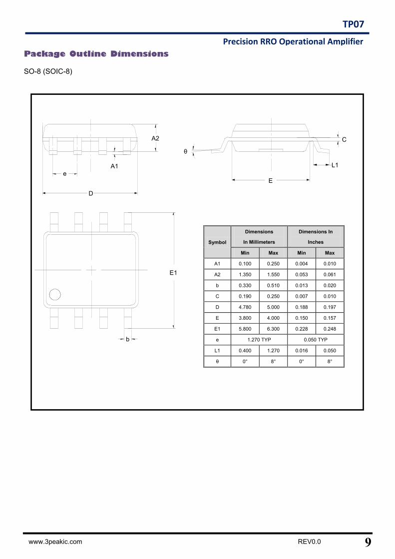
Package Outline Dimensions
SO-8 (SOIC-8)
Symbol
Dimensions
In Millimeters
Dimensions In
Inches
Min Max Min Max
A1 0.100 0.250 0.004 0.010
A2 1.350 1.550 0.053 0.061
b 0.330 0.510 0.013 0.020
C 0.190 0.250 0.007 0.010
D 4.780 5.000 0.188 0.197
E 3.800 4.000 0.150 0.157
E1 5.800 6.300 0.228 0.248
e 1.270 TYP 0.050 TYP
L1 0.400 1.270 0.016 0.050
θ 0° 8° 0° 8°
![p í 3 ò X k - transgenic.co.jp · Ä J ò . V 4 i ¥ p í 3 ò X k V ¥ T u - g Ô O m ç { æ ù L < · ¸ Õ b ª þ Í ¤ O T Ç y õ ] ì k z k U T](https://static.fdocument.org/doc/165x107/5cf6a58088c99387248b86b9/p-i-3-o-x-k-ae-j-o-v-4-i-p-i-3-o-x-k-v-t-u-g-o-o-m-c-ae.jpg)

![k‑p‑t‑c {‑µ³ F‑ ‑g‑p ‑]‑p¶](https://static.fdocument.org/doc/165x107/61718417c41ca10cb91c5710/kptc-.jpg)

![Mekaniikka Dynamiikka Kinematiikka - teho- · PDF file2 Keskimääräinen teho P k ' n W t [P k] = J/s = W, watti. Hetkellinen teho P ' Fv Hyötysuhde η ' P anto P otto ' E anto E](https://static.fdocument.org/doc/165x107/5a9e4c197f8b9a75458d2c02/mekaniikka-dynamiikka-kinematiikka-teho-keskimrinen-teho-p-k-n-w-t-p-k-.jpg)


![arXiv:1402.5501v3 [hep-ph] 16 Apr 2014 · 2018. 10. 23. · 3 k 2 (a) k 1 P 1 −k 1 P 2 −k 2 (b) b u FIG. 1. Leading-order quark diagrams for theB → π transition form factor](https://static.fdocument.org/doc/165x107/5fee6178cff77a4bc67401b8/arxiv14025501v3-hep-ph-16-apr-2014-2018-10-23-3-k-2-a-k-1-p-1-ak-1.jpg)