LM321/LM358/LM324 3 P E A K - szlcsc.com
16
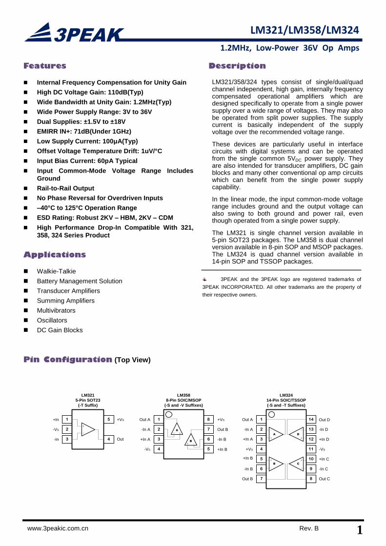
3PEAK 1 LM321/LM358/LM324 1.2MHz, Low-Power 36V Op Amps www.3peakic.com.cn Rev. B Features Internal Frequency Compensation for Unity Gain High DC Voltage Gain: 110dB(Typ) Wide Bandwidth at Unity Gain: 1.2MHz(Typ) Wide Power Supply Range: 3V to 36V Dual Supplies: ±1.5V to ±18V EMIRR IN+: 71dB(Under 1GHz) Low Supply Current: 100μA(Typ) Offset Voltage Temperature Drift: 1uV/°C Input Bias Current: 60pA Typical Input Common-Mode Voltage Range Includes Ground Rail-to-Rail Output No Phase Reversal for Overdriven Inputs –40°C to 125°C Operation Range ESD Rating: Robust 2KV – HBM, 2KV – CDM High Performance Drop-In Compatible With 321, 358, 324 Series Product Applications Walkie-Talkie Battery Management Solution Transducer Amplifiers Summing Amplifiers Multivibrators Oscillators DC Gain Blocks Pin Configuration (Top View) Description LM321/358/324 types consist of single/dual/quad channel independent, high gain, internally frequency compensated operational amplifiers which are designed specifically to operate from a single power supply over a wide range of voltages. They may also be operated from split power supplies. The supply current is basically independent of the supply voltage over the recommended voltage range. These devices are particularly useful in interface circuits with digital systems and can be operated from the single common 5V DC power supply. They are also intended for transducer amplifiers, DC gain blocks and many other conventional op amp circuits which can benefit from the single power supply capability. In the linear mode, the input common-mode voltage range includes ground and the output voltage can also swing to both ground and power rail, even though operated from a single power supply. The LM321 is single channel version available in 5-pin SOT23 packages. The LM358 is dual channel version available in 8-pin SOP and MSOP packages. The LM324 is quad channel version available in 14-pin SOP and TSSOP packages. 3PEAK and the 3PEAK logo are registered trademarks of 3PEAK INCORPORATED. All other trademarks are the property of their respective owners. LM321 5-Pin SOT23 (-T Suffix) 4 5 3 2 1 +In -VS -In Out +VS 14 13 12 11 10 9 8 6 5 7 3 2 1 4 Out A -VS +In A -In A +VS D A C B Out D +In D -In D Out B +In B -In B Out C +In C -In C LM324 14-Pin SOIC/TSSOP (-S and -T Suffixes) 8 6 5 7 3 2 1 4 Out A -VS +In A -In A +VS +In B -In B Out B A B LM358 8-Pin SOIC/MSOP (-S and -V Suffixes)
Transcript of LM321/LM358/LM324 3 P E A K - szlcsc.com
3PEAK
1
LM321/LM358/LM324
1.2MHz, Low-Power 36V Op Amps
www.3peakic.com.cn Rev. B
Features
Internal Frequency Compensation for Unity Gain
High DC Voltage Gain: 110dB(Typ)
Wide Bandwidth at Unity Gain: 1.2MHz(Typ)
Wide Power Supply Range: 3V to 36V
Dual Supplies: ±1.5V to ±18V
EMIRR IN+: 71dB(Under 1GHz)
Low Supply Current: 100μA(Typ)
Offset Voltage Temperature Drift: 1uV/°C
Input Bias Current: 60pA Typical
Input Common-Mode Voltage Range Includes
Ground
Rail-to-Rail Output
No Phase Reversal for Overdriven Inputs
–40°C to 125°C Operation Range
ESD Rating: Robust 2KV – HBM, 2KV – CDM
High Performance Drop-In Compatible With 321,
358, 324 Series Product
Applications
Walkie-Talkie
Battery Management Solution
Transducer Amplifiers
Summing Amplifiers
Multivibrators
Oscillators
DC Gain Blocks
Pin Configuration (Top View)
Description
LM321/358/324 types consist of single/dual/quad channel independent, high gain, internally frequency compensated operational amplifiers which are designed specifically to operate from a single power supply over a wide range of voltages. They may also be operated from split power supplies. The supply current is basically independent of the supply voltage over the recommended voltage range.
These devices are particularly useful in interface circuits with digital systems and can be operated from the single common 5VDC power supply. They are also intended for transducer amplifiers, DC gain blocks and many other conventional op amp circuits which can benefit from the single power supply capability.
In the linear mode, the input common-mode voltage range includes ground and the output voltage can also swing to both ground and power rail, even though operated from a single power supply.
The LM321 is single channel version available in 5-pin SOT23 packages. The LM358 is dual channel version available in 8-pin SOP and MSOP packages. The LM324 is quad channel version available in 14-pin SOP and TSSOP packages.
3PEAK and the 3PEAK logo are registered trademarks of
3PEAK INCORPORATED. All other trademarks are the property of
their respective owners.
LM321
5-Pin SOT23
(-T Suffix)
4
5
3
2
1+In
-VS
-In Out
+VS 14
13
12
11
10
9
8
6
5
7
3
2
1
4
Out A
-VS
+In A
-In A
+VS
DA
CB
Out D
+In D
-In D
Out B
+In B
-In B
Out C
+In C
-In C
LM324
14-Pin SOIC/TSSOP
(-S and -T Suffixes)
8
6
5
7
3
2
1
4
Out A
-VS
+In A
-In A
+VS
+In B
-In B
Out BA
B
LM358
8-Pin SOIC/MSOP
(-S and -V Suffixes)
2 Rev. B www.3peakic.com.cn
LM321 / LM358 / LM324
1.2MHz, Low-Power 36V Op Amps
Order Information
Model Name Order Number Package Transport Media, Quantity Marking
Information
LM321 LM321-TR 5-Pin SOT23 Tape and Reel, 3,000 H21
LM358 LM358-SR 8-Pin SOP Tape and Reel, 4,000 LM358
LM358-VR 8-Pin MSOP Tape and Reel, 3,000 LM358
LM324 LM324-SR 14-Pin SOP Tape and Reel, 2,500 LM324
LM324-TR 14-Pin TSSOP Tape and Reel, 3,000 LM324
Absolute Maximum Ratings Note 1
Supply Voltage: V+ – V
– Note 2................................. 42V
Input Voltage................................ V– – 0.3 to V
+ + 0.3
Input Current: +IN, –IN Note 3............................ ±20mA
Differential Input Voltage..................................... ±42V
Output Short-Circuit Duration Note 4…............... Infinite
Current at Supply Pins……………............... ±60mA
Operating Temperature Range........–40°C to 125°C
Maximum Junction Temperature................... 150°C
Storage Temperature Range.......... –65°C to 150°C
Lead Temperature (Soldering, 10 sec) ......... 260°C
Note 1: Stresses beyond those listed under Absolute Maximum Ratings may cause permanent damage to the device. Exposure to any Absolute Maximum
Rating condition for extended periods may affect device reliability and lifetime.
Note 2: The op amp supplies must be established simultaneously, with, or before, the application of any input signals.
Note 3: The inputs are protected by ESD protection diodes to each power supply. If the input extends more than 500mV beyond the power supply, the input
current should be limited to less than 10mA.
Note 4: A heat sink may be required to keep the junction temperature below the absolute maximum. This depends on the power supply voltage and how many
amplifiers are shorted. Thermal resistance varies with the amount of PC board metal connected to the package. The specified values are for short traces
connected to the leads.
ESD, Electrostatic Discharge Protection
Symbol Parameter Condition Minimum Level Unit
HBM Human Body Model ESD MIL-STD-883H Method 3015.8 2 kV
CDM Charged Device Model ESD JEDEC-EIA/JESD22-C101E 2 kV
Thermal Resistance
Package Type θJA θJC Unit
5-Pin SOT23 250 81 ° C/W
8-Pin SOP 158 43 ° C/W
8-Pin MSOP 210 45 ° C/W
14-Pin SOP 120 36 ° C/W
14-Pin TSSOP 180 35 ° C/W
3
LM321/LM358/ LM324
1.2MHz, Low-Power 36V Op Amps
www.3peakic.com.cn Rev. B
Electrical Characteristics
The specifications are at TA = 27° C. VS = 5V, VCM = VOUT =2.5V, RL = 2kΩ, CL =100pF.Unless otherwise noted.
SYMBOL PARAMETER CONDITIONS MIN TYP MAX UNITS
VOS Input Offset Voltage VS = 5 V, VCM = 2.5V and VCM = 0V -3 ±1 3 mV
VS = 30 V, VCM = 15V and VCM = 0V -3 ±1 3 mV
VOS TC Input Offset Voltage Drift -40° C to 125° C 1 μV/° C
IB Input Bias Current TA = 27 ° C 60 pA
TA = 85 ° C 200 pA
IOS Input Offset Current 0.001 pA
Vn Input Voltage Noise f = 0.1Hz to 10Hz 10 μVPP
en Input Voltage Noise Density f = 1kHz 48 nV/√Hz
in Input Current Noise f = 1kHz 2 fA/√Hz
CIN Input Capacitance Differential
Common Mode
2.5
5 pF
CMRR Common Mode Rejection Ratio DC, VCM=0V to 28V 80 120 dB
VCM Common-mode Input Voltage
Range VS = 5 V to 30V V– V+-2 V
PSRR Power Supply Rejection Ratio VS = 5 V to 30V 90 120 dB
AVOL Open-Loop Large Signal Gain VS = 15 V, VO = 1 V to 11 V, RL = 2 kΩ 98 110 dB
VOH Output Swing from Supply Rail RLOAD = 10kΩ, VS = ± 15 V 14.70 14.75 V
RLOAD = 2kΩ, VS = ± 15 V 13.70 13.90 V
VOL Output Swing from Supply Rail
RLOAD = 10kΩ , VS = ± 15 V -14.85 -14.70 V
RLOAD = 2kΩ, VS = ± 15 V -14.25 -14.10 V
RLOAD ≥ 10 kΩ, VS = 15 V 5 mV
ROUT Closed-Loop Output Impedance G = 1, f =1kHz, IOUT = 0 0.002 Ω
RO Open-Loop Output Impedance f = 1kHz, IOUT = 0 120 Ω
ISC Output Short-Circuit Current Sink or source current, VS = 30V 20 35 mA
VS Supply Voltage 3 36 V
IQ Quiescent Current per Amplifier VS = 5V, No load 100 150 μA
VS = 30V, No load 110 200 μA
PM Phase Margin RLOAD = 1kΩ, CLOAD = 100pF 62 °
GM Gain Margin RLOAD = 1kΩ, CLOAD = 60pF 18 dB
GBWP Gain-Bandwidth Product f = 1kHz 1.2 MHz
SR Slew Rate at unity gain AV = 1, VOUT = -10V to 10V, CLOAD =60pF,
RLOAD = 10kΩ, VS = ± 15V 0.55 V/μs
FPBW Full Power Bandwidth Note 1 17.5 kHz
tS Settling Time, 0.1%
Settling Time, 0.01% AV = 1.5V to 3.5V Step
2.8
3.1 μs
THD+N Total Harmonic Distortion and
Noise f = 1kHz, AV =1, RL = 2kΩ, VOUT = 1Vp-p 0.001 %
Xtalk Channel Separation f = 1 kHz to 20 kHz 80 dB
Note 1: Full power bandwidth is calculated from the slew rate FPBW = SR/π • VP-P
4 Rev. B www.3peakic.com.cn
LM321 / LM358 / LM324
1.2MHz, Low-Power 36V Op Amps
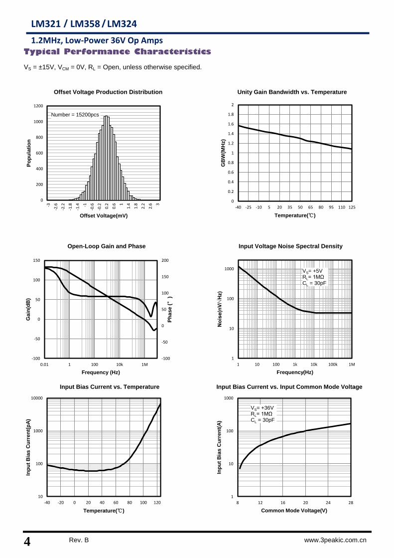
Typical Performance Characteristics
VS = ±15V, VCM = 0V, RL = Open, unless otherwise specified.
Offset Voltage Production Distribution Unity Gain Bandwidth vs. Temperature
Open-Loop Gain and Phase Input Voltage Noise Spectral Density
Input Bias Current vs. Temperature Input Bias Current vs. Input Common Mode Voltage
0
200
400
600
800
1000
1200
-3
-2.6
-2.2
-1.8
-1.4 -1
-0.6
-0.2 0.2
0.6 1
1.4
1.8
2.2
2.6 3
Po
pu
lati
on
Offset Voltage(mV)
Number = 15200pcs
0
0.2
0.4
0.6
0.8
1
1.2
1.4
1.6
1.8
2
-40 -25 -10 5 20 35 50 65 80 95 110 125
GB
W(M
Hz)
Temperature(℃)
-100
-50
0
50
100
150
200
-100
-50
0
50
100
150
0.01 1 100 10k 1M
Ph
ase (°
)
Gain
(dB
)
Frequency (Hz)
1
10
100
1000
1 10 100 1k 10k 100k 1M
Noise(nV/√Hz)
Frequency(Hz)
VS= +5V RL= 1MΩ
CL = 30pF
10
100
1000
10000
-40 -20 0 20 40 60 80 100 120
Inp
ut
Bia
s C
urr
en
t(p
A)
Temperature(℃)
1
10
100
1000
8 12 16 20 24 28
Inp
ut
Bia
s C
urr
en
t(A
)
Common Mode Voltage(V)
VS= +36V RL= 1MΩ
CL = 30pF
5
LM321/LM358/ LM324
1.2MHz, Low-Power 36V Op Amps
www.3peakic.com.cn Rev. B
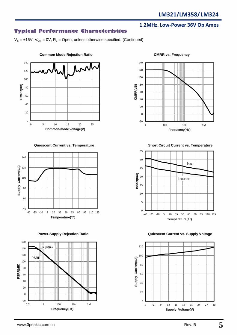
Typical Performance Characteristics
VS = ±15V, VCM = 0V, RL = Open, unless otherwise specified. (Continued)
Common Mode Rejection Ratio CMRR vs. Frequency
Quiescent Current vs. Temperature Short Circuit Current vs. Temperature
Power-Supply Rejection Ratio Quiescent Current vs. Supply Voltage
0
20
40
60
80
100
120
140
0 5 10 15 20 25
CM
RR
(dB
)
Common-mode voltage(V)
-20
0
20
40
60
80
100
120
140
1 100 10k 1M
CM
RR
(dB
)
Frequency(Hz)
40
60
80
100
120
140
-40 -25 -10 5 20 35 50 65 80 95 110 125
Su
pp
ly
Cu
rren
t(u
A)
Temperature(℃)
0
5
10
15
20
25
30
35
-40 -25 -10 5 20 35 50 65 80 95 110 125
Ish
ort
(mA
)
Temperature(℃)
ISINK
ISOURCE
-20
0
20
40
60
80
100
120
140
160
0.01 1 100 10k 1M
PS
RR
(dB
)
Frequency(Hz)
PSRR+
PSRR-
0
20
40
60
80
100
120
3 6 9 12 15 18 21 24 27 30
Su
pp
ly
Cu
rren
t(u
A)
Supply Voltage(V)
6 Rev. B www.3peakic.com.cn
LM321 / LM358 / LM324
1.2MHz, Low-Power 36V Op Amps
Typical Performance Characteristics
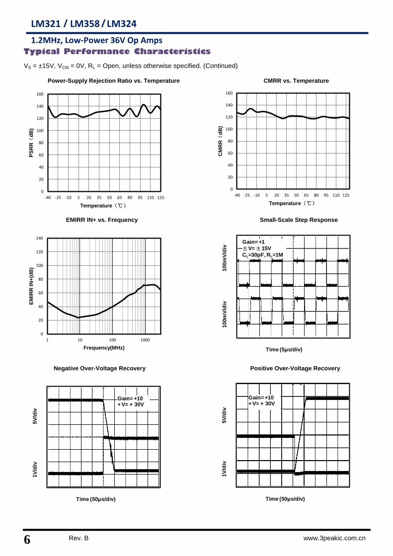
VS = ±15V, VCM = 0V, RL = Open, unless otherwise specified. (Continued)
Power-Supply Rejection Ratio vs. Temperature CMRR vs. Temperature
EMIRR IN+ vs. Frequency Small-Scale Step Response
Negative Over-Voltage Recovery Positive Over-Voltage Recovery
0
20
40
60
80
100
120
140
160
-40 -25 -10 5 20 35 50 65 80 95 110 125
PS
RR(
dB
)
Temperature(℃)
0
20
40
60
80
100
120
140
160
-40 -25 -10 5 20 35 50 65 80 95 110 125
CM
RR(
dB
)
Temperature(℃)
0
20
40
60
80
100
120
140
1 10 100 1000
EM
IRR
IN
+(d
B)
Frequency(MHz)
100m
V/d
iv
1
00m
V/d
iv
Time (5μs/div)
Gain= +1
±V= ±15V
CL=30pF, RL=1M
1V
/div
5
V/d
iv
Time (50μs/div)
Gain= +10+ V= + 30V
1V
/div
5
V/d
iv
Time (50μs/div)
Gain= +10+ V= + 30V
7
LM321/LM358/ LM324
1.2MHz, Low-Power 36V Op Amps
www.3peakic.com.cn Rev. B
Typical Performance Characteristics
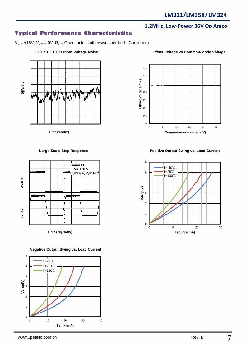
VS = ±15V, VCM = 0V, RL = Open, unless otherwise specified. (Continued)
0.1 Hz TO 10 Hz Input Voltage Noise Offset Voltage vs Common-Mode Voltage
Large-Scale Step Response Positive Output Swing vs. Load Current
Negative Output Swing vs. Load Current
Time (1s/div)
5μ
V/d
iv
0
0.2
0.4
0.6
0.8
1
1.2
1.4
0 5 10 15 20 25
Off
set
vo
ltag
e(m
V)
Common-mode voltage(V)
2V
/div
2V
/div
Time (20μs/div)
Gain= +1
±V= ±15V
CL=30pF, RL=1M
0
1
2
3
4
5
6
0 10 20 30
Vd
rop
(V)
I source(mA)
T=-40℃
T=25℃
T=130℃
0
1
2
3
4
5
6
0 10 20 30 40
Vd
rop
(V)
I sink (mA)
T=-40℃
T=25℃
T=130℃
8 Rev. B www.3peakic.com.cn
LM321 / LM358 / LM324
1.2MHz, Low-Power 36V Op Amps
Pin Functions
-IN: Inverting Input of the Amplifier.
+IN: Non-Inverting Input of Amplifier.
OUT: Amplifier Output. The voltage range extends to
within mV of each supply rail.
V+ or +Vs: Positive Power Supply. Typically the voltage
is from 3V to 36V. Split supplies are possible as long
as the voltage between V+ and V– is between 3V and
36V. A bypass capacitor of 0.1μF as close to the part as
possible should be used between power supply pins or
between supply pins and ground.
V- or -Vs: Negative Power Supply. It is normally tied to
ground. It can also be tied to a voltage other than
ground as long as the voltage between V+ and V– is from
3V to 36V. If it is not connected to ground, bypass it
with a capacitor of 0.1μF as close to the part as
possible.
Operation
The LM321/358/324 output signal range extends beyond the negative and positive power supplies. The intput can even
extend all the way to the negative supply. The Class-AB control buffer and output bias stage uses a proprietary
compensation technique to take full advantage of the process technology to drive very high capacitive loads. This is
evident from the transient over shoot measurement plots in the Typical Performance Characteristics.
Applications Information
High Supply Voltage and Low Power Consumption
The LM321/358/324 of operational amplifiers can operate with power supply voltages from 3V to 36V. Each amplifier
draws only 100μA quiescent current. The low supply voltage capability and low supply current are ideal for portable
applications demanding HIGH CAPACITIVE LOAD DRIVING CAPABILITY and WIDE BANDWIDTH. The
LM321/358/324 is optimized for wide bandwidth low power applications. They have an industry leading high GBWP to
power ratio and are unity gain stable for 10nf CAPACITIVE load. When the load capacitance increases, the increased
capacitance at the output pushed the non-dominant pole to lower frequency in the open loop frequency response,
lowering the phase and gain margin. Higher gain configurations tend to have better capacitive drive capability than
lower gain configurations due to lower closed loop bandwidth and hence higher phase margin.
Low Input Referred Noise
The LM321/358/324 provides a low input referred noise density of 48nV/√Hz at 1kHz. The voltage noise will grow
slowly with the frequency in wideband range, and the input voltage noise is typically 10μVP-P at the frequency of 0.1Hz
to 10Hz.
Low Input Offset Voltage
The LM321/358/324 has a low offset voltage tolerance of 3mV maximum which is essential for precision applications.
The offset voltage is trimmed with a proprietary trim algorithm to ensure low offset voltage for precision signal
processing requirement.
Low Input Bias Current
The LM321/358/324 is a CMOS OPA family and features very low input bias current in pA range. The low input bias
current allows the amplifiers to be used in applications with high resistance sources. Care must be taken to minimize
PCB Surface Leakage. See below section on “PCB Surface Leakage” for more details.
PCB Surface Leakage
9
LM321/LM358/ LM324
1.2MHz, Low-Power 36V Op Amps
www.3peakic.com.cn Rev. B
In applications where low input bias current is critical, Printed Circuit Board (PCB) surface leakage effects need to be
considered. Surface leakage is caused by humidity, dust or other contamination on the board. Under low humidity
conditions, a typical resistance between nearby traces is 1012
Ω. A 5V difference would cause 5pA of current to flow,
which is greater than the LM321/358/324 OPA‟s input bias current at +27°C (±1pA, typical). It is recommended to use
multi-layer PCB layout and route the OPA‟s -IN and +IN signal under the PCB surface.
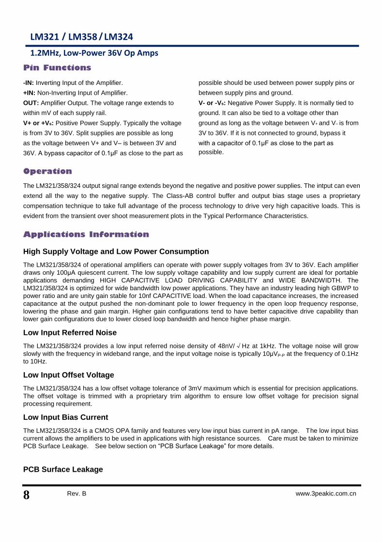
The effective way to reduce surface leakage is to use a guard ring around sensitive pins (or traces). The guard
ring is biased at the same voltage as the sensitive pin. An example of this type of layout is shown in Figure 1 for
Inverting Gain application.
1. For Non-Inverting Gain and Unity-Gain Buffer:
a) Connect the non-inverting pin (VIN+) to the input with a wire that does not touch the PCB surface.
b) Connect the guard ring to the inverting input pin (VIN–). This biases the guard ring to the Common Mode input voltage.
2. For Inverting Gain and Trans-impedance Gain Amplifiers (convert current to voltage, such as photo detectors):
a) Connect the guard ring to the non-inverting input pin (VIN+). This biases the guard ring to the same reference voltage as
the op-amp (e.g., VS/2 or ground).
b) Connect the inverting pin (VIN–) to the input with a wire that does not touch the PCB surface.
VIN+ VIN- +VSGuard Ring
Figure 1
Ground Sensing and Rail to Rail Output
The LM321/358/324 has excellent output drive capability, delivering over 35mA of output drive current. The output
stage is a rail-to-rail topology that is capable of swinging to within 5mV of either rail. Since the inputs can go 100mV
beyond either rail, the op-amp can easily perform „True Ground Sensing‟.
The maximum output current is a function of total supply voltage. As the supply voltage to the amplifier increases, the
output current capability also increases. Attention must be paid to keep the junction temperature of the IC below 150°C
when the output is in continuous short-circuit. The output of the amplifier has reverse-biased ESD diodes connected to
each supply. The output should not be forced more than 0.5V beyond either supply, otherwise current will flow through
these diodes.
ESD
The LM321/358/324 has reverse-biased ESD protection diodes on all inputs and output. Input and out pins cannot be
biased more than 200mV beyond either supply rail.
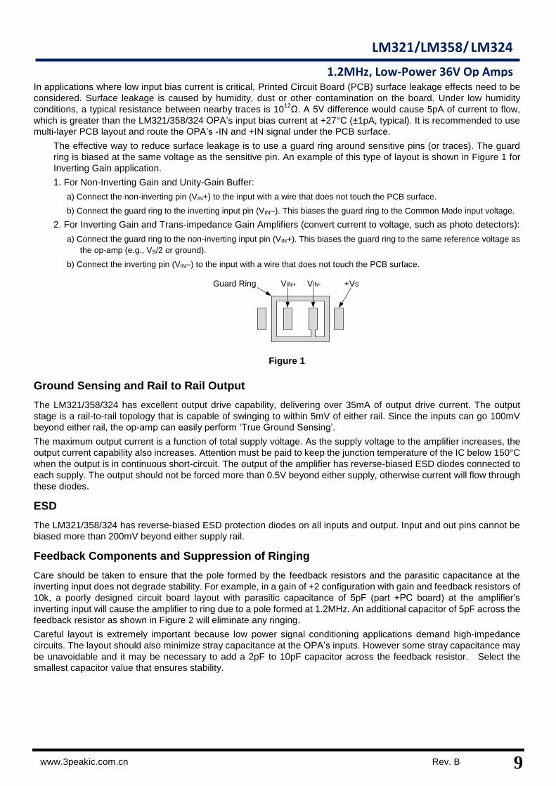
Feedback Components and Suppression of Ringing
Care should be taken to ensure that the pole formed by the feedback resistors and the parasitic capacitance at the
inverting input does not degrade stability. For example, in a gain of +2 configuration with gain and feedback resistors of
10k, a poorly designed circuit board layout with parasitic capacitance of 5pF (part +PC board) at the amplifier‟s
inverting input will cause the amplifier to ring due to a pole formed at 1.2MHz. An additional capacitor of 5pF across the
feedback resistor as shown in Figure 2 will eliminate any ringing.
Careful layout is extremely important because low power signal conditioning applications demand high-impedance
circuits. The layout should also minimize stray capacitance at the OPA‟s inputs. However some stray capacitance may
be unavoidable and it may be necessary to add a 2pF to 10pF capacitor across the feedback resistor. Select the
smallest capacitor value that ensures stability.
10 Rev. B www.3peakic.com.cn
LM321 / LM358 / LM324
1.2MHz, Low-Power 36V Op Amps
10kΩ
5pF
10kΩ CPAR
VIN
VOUT
Figure 2
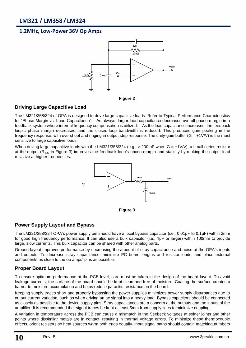
Driving Large Capacitive Load
The LM321/358/324 of OPA is designed to drive large capacitive loads. Refer to Typical Performance Characteristics
for “Phase Margin vs. Load Capacitance”. As always, larger load capacitance decreases overall phase margin in a
feedback system where internal frequency compensation is utilized. As the load capacitance increases, the feedback
loop‟s phase margin decreases, and the closed-loop bandwidth is reduced. This produces gain peaking in the
frequency response, with overshoot and ringing in output step response. The unity-gain buffer (G = +1V/V) is the most
sensitive to large capacitive loads.
When driving large capacitive loads with the LM321/358/324 (e.g., > 200 pF when G = +1V/V), a small series resistor
at the output (RISO in Figure 3) improves the feedback loop‟s phase margin and stability by making the output load
resistive at higher frequencies.
VIN
VOUT
CLOAD
RISO
Figure 3
Power Supply Layout and Bypass
The LM321/358/324 OPA‟s power supply pin should have a local bypass capacitor (i.e., 0.01μF to 0.1μF) within 2mm
for good high frequency performance. It can also use a bulk capacitor (i.e., 1μF or larger) within 100mm to provide
large, slow currents. This bulk capacitor can be shared with other analog parts.
Ground layout improves performance by decreasing the amount of stray capacitance and noise at the OPA‟s inputs
and outputs. To decrease stray capacitance, minimize PC board lengths and resistor leads, and place external
components as close to the op amps‟ pins as possible.
Proper Board Layout
To ensure optimum performance at the PCB level, care must be taken in the design of the board layout. To avoid
leakage currents, the surface of the board should be kept clean and free of moisture. Coating the surface creates a
barrier to moisture accumulation and helps reduce parasitic resistance on the board.
Keeping supply traces short and properly bypassing the power supplies minimizes power supply disturbances due to
output current variation, such as when driving an ac signal into a heavy load. Bypass capacitors should be connected
as closely as possible to the device supply pins. Stray capacitances are a concern at the outputs and the inputs of the
amplifier. It is recommended that signal traces be kept at least 5mm from supply lines to minimize coupling.
A variation in temperature across the PCB can cause a mismatch in the Seebeck voltages at solder joints and other
points where dissimilar metals are in contact, resulting in thermal voltage errors. To minimize these thermocouple
effects, orient resistors so heat sources warm both ends equally. Input signal paths should contain matching numbers
11
LM321/LM358/ LM324
1.2MHz, Low-Power 36V Op Amps
www.3peakic.com.cn Rev. B
and types of components, where possible to match the number and type of thermocouple junctions. For example,
dummy components such as zero value resistors can be used to match real resistors in the opposite input path.
Matching components should be located in close proximity and should be oriented in the same manner. Ensure leads
are of equal length so that thermal conduction is in equilibrium. Keep heat sources on the PCB as far away from
amplifier input circuitry as is practical.
The use of a ground plane is highly recommended. A ground plane reduces EMI noise and also helps to maintain a
constant temperature across the circuit board.
Instrumentation Amplifier
The LM321/358/324 OPA is well suited for conditioning sensor signals in battery-powered applications. Figure 4
shows a two op-amp instrumentation amplifier, using the LM321/358/324 OPA.
The circuit works well for applications requiring rejection of Common Mode noise at higher gains. The reference
voltage (VREF) is supplied by a low-impedance source. In single voltage supply applications, VREF is typically VS/2.
VREF VOUT
RG
R2 R2 R1R1
V2
V1
1 11 2
2
2=( )(1 )OUT REF
G
R RV V V V
R R
Figure 4
Two-Pole Micro-power Sallen-Key Low-Pass Filter
Figure 5 shows a micro-power two-pole Sallen-Key Low-Pass Filter with 400Hz cut-off frequency. For best results,
the filter‟s cut-off frequency should be 8 to 10 times lower than the OPA‟s crossover frequency. Additional OPA‟s
phase margin shift can be avoided if the OPA‟s bandwidth-to-signal ratio is greater than 8. The design equations for
the 2-pole Sallen-Key low-pass filter are given below with component values selected to set a 400Hz low-pass filter
cutoff frequency:
R1
1MΩ
R2
1MΩ
C1
400pF
C2
400pF
R3
2MΩ
R4
2MΩ
VIN
VOUT
1 2
1 2
-3dB
3 4 3 4
R = R = R = 1M
C = C = C = 400pF
Q = Filter Peaking Factor = 1
f = 1/(2 ) = 400
R = R /(2-1/Q) ; with Q = 1, R =R
RC Hz
Figure 5
12 Rev. B www.3peakic.com.cn
LM321 / LM358 / LM324
1.2MHz, Low-Power 36V Op Amps
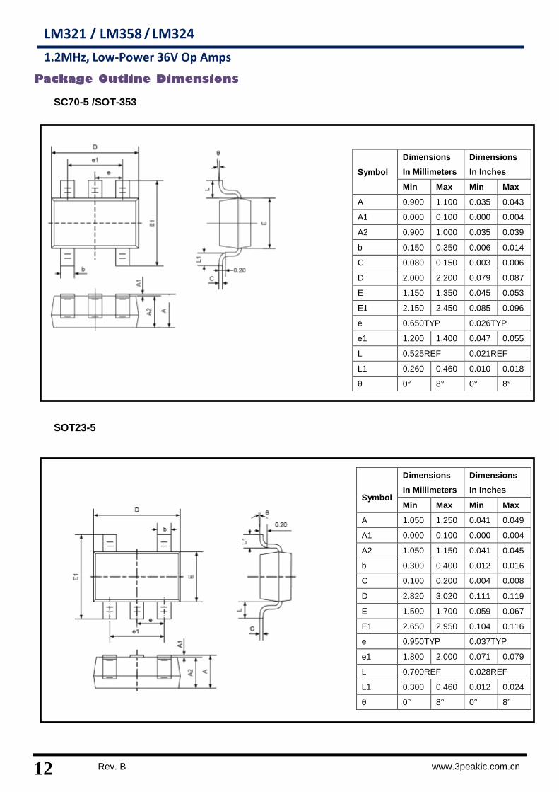
Package Outline Dimensions
SC70-5 /SOT-353
SOT23-5
Symbol
Dimensions
In Millimeters
Dimensions
In Inches
Min Max Min Max
A 1.050 1.250 0.041 0.049
A1 0.000 0.100 0.000 0.004
A2 1.050 1.150 0.041 0.045
b 0.300 0.400 0.012 0.016
C 0.100 0.200 0.004 0.008
D 2.820 3.020 0.111 0.119
E 1.500 1.700 0.059 0.067
E1 2.650 2.950 0.104 0.116
e 0.950TYP 0.037TYP
e1 1.800 2.000 0.071 0.079
L 0.700REF 0.028REF
L1 0.300 0.460 0.012 0.024
θ 0° 8° 0° 8°
Symbol
Dimensions
In Millimeters
Dimensions
In Inches
Min Max Min Max
A 0.900 1.100 0.035 0.043
A1 0.000 0.100 0.000 0.004
A2 0.900 1.000 0.035 0.039
b 0.150 0.350 0.006 0.014
C 0.080 0.150 0.003 0.006
D 2.000 2.200 0.079 0.087
E 1.150 1.350 0.045 0.053
E1 2.150 2.450 0.085 0.096
e 0.650TYP 0.026TYP
e1 1.200 1.400 0.047 0.055
L 0.525REF 0.021REF
L1 0.260 0.460 0.010 0.018
θ 0° 8° 0° 8°
13
LM321/LM358/ LM324
1.2MHz, Low-Power 36V Op Amps
www.3peakic.com.cn Rev. B
D
E1
b
E
A1
A2
e
θ
L1
C
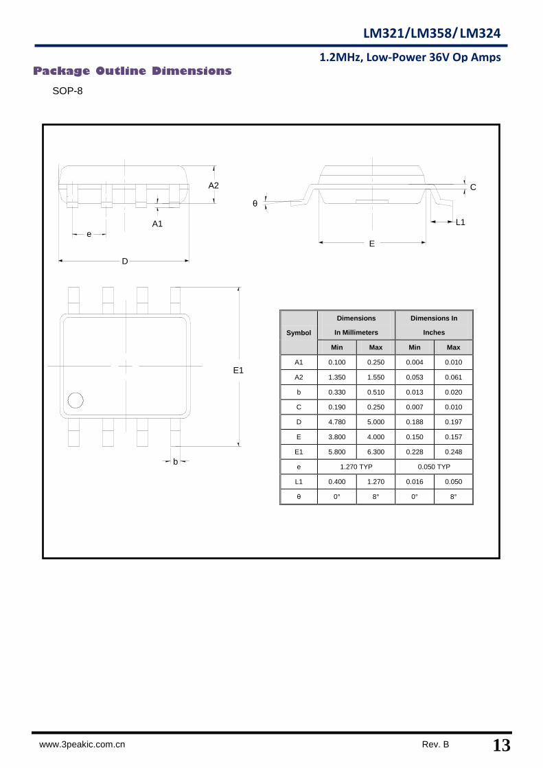
Package Outline Dimensions
SOP-8
Symbol
Dimensions
In Millimeters
Dimensions In
Inches
Min Max Min Max
A1 0.100 0.250 0.004 0.010
A2 1.350 1.550 0.053 0.061
b 0.330 0.510 0.013 0.020
C 0.190 0.250 0.007 0.010
D 4.780 5.000 0.188 0.197
E 3.800 4.000 0.150 0.157
E1 5.800 6.300 0.228 0.248
e 1.270 TYP 0.050 TYP
L1 0.400 1.270 0.016 0.050
θ 0° 8° 0° 8°
14 Rev. B www.3peakic.com.cn
LM321 / LM358 / LM324
1.2MHz, Low-Power 36V Op Amps
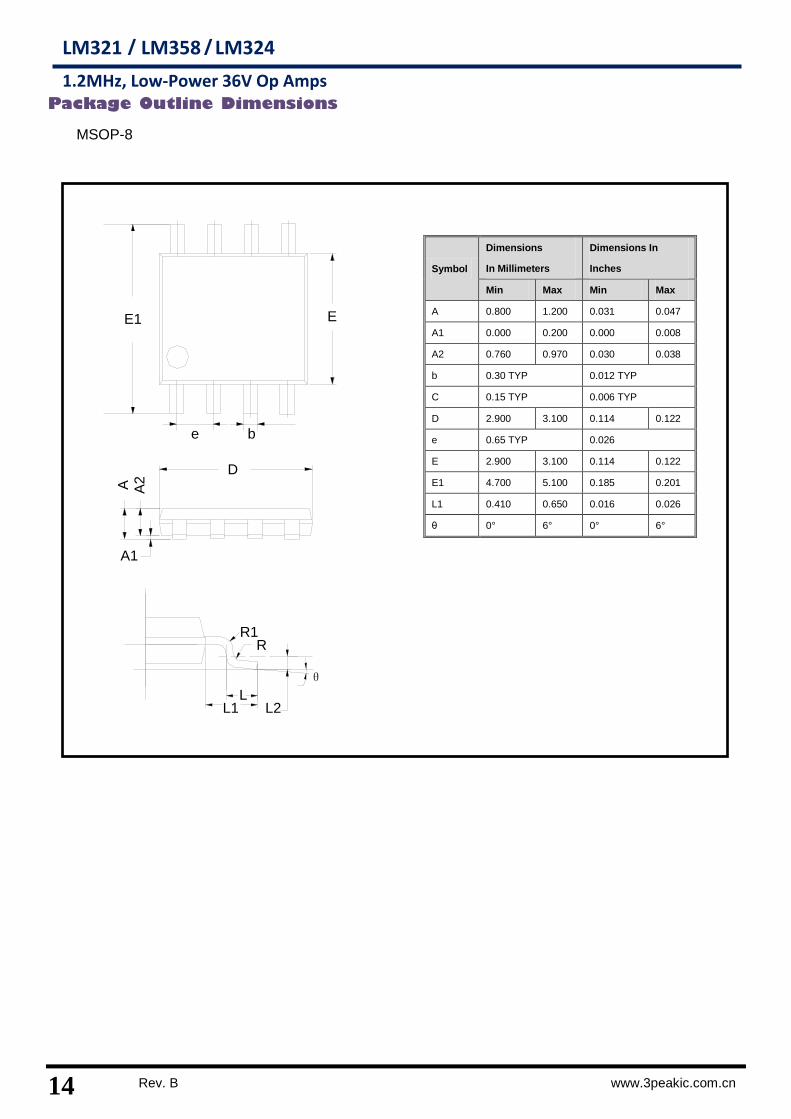
Package Outline Dimensions
MSOP-8
Symbol
Dimensions
In Millimeters
Dimensions In
Inches
Min Max Min Max
A 0.800 1.200 0.031 0.047
A1 0.000 0.200 0.000 0.008
A2 0.760 0.970 0.030 0.038
b 0.30 TYP 0.012 TYP
C 0.15 TYP 0.006 TYP
D 2.900 3.100 0.114 0.122
e 0.65 TYP 0.026
E 2.900 3.100 0.114 0.122
E1 4.700 5.100 0.185 0.201
L1 0.410 0.650 0.016 0.026
θ 0° 6° 0° 6°
E1
e
E
A1
A2A
D
L1 L2L
RR1
θ
b
15
LM321/LM358/ LM324
1.2MHz, Low-Power 36V Op Amps
www.3peakic.com.cn Rev. B
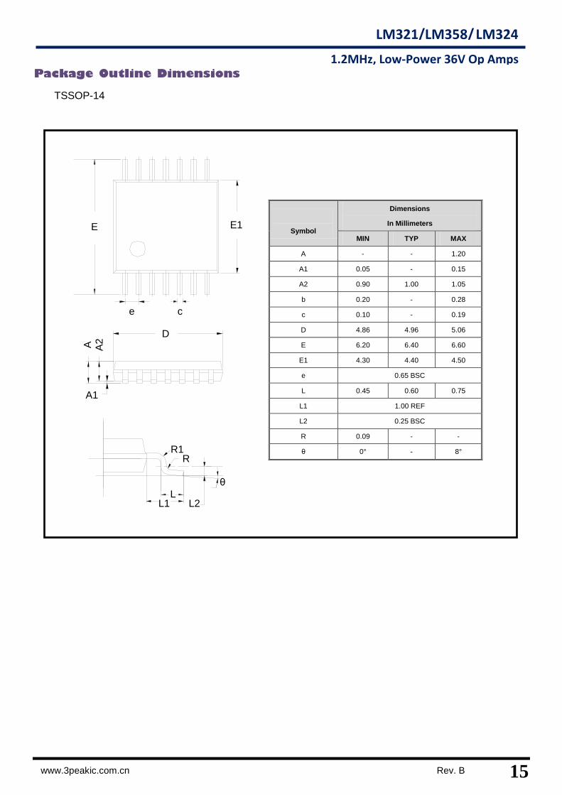
Package Outline Dimensions
TSSOP-14
Symbol
Dimensions
In Millimeters
MIN TYP MAX
A - - 1.20
A1 0.05 - 0.15
A2 0.90 1.00 1.05
b 0.20 - 0.28
c 0.10 - 0.19
D 4.86 4.96 5.06
E 6.20 6.40 6.60
E1 4.30 4.40 4.50
e 0.65 BSC
L 0.45 0.60 0.75
L1 1.00 REF
L2 0.25 BSC
R 0.09 - -
θ 0° - 8°
E
e
E1
A1
A2A
D
L1 L2L
RR1
θ
c
16 Rev. B www.3peakic.com.cn
LM321 / LM358 / LM324
1.2MHz, Low-Power 36V Op Amps
θ
e b
E1 E
D
A1
A A2
L1L
L2
Package Outline Dimensions
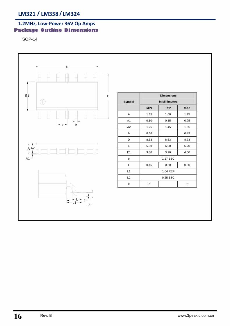
SOP-14
Symbol
Dimensions
In Millimeters
MIN TYP MAX
A 1.35 1.60 1.75
A1 0.10 0.15 0.25
A2 1.25 1.45 1.65
b 0.36 0.49
D 8.53 8.63 8.73
E 5.80 6.00 6.20
E1 3.80 3.90 4.00
e 1.27 BSC
L 0.45 0.60 0.80
L1 1.04 REF
L2 0.25 BSC
θ 0° 8°


![arXiv:1402.5501v3 [hep-ph] 16 Apr 2014 · 2018. 10. 23. · 3 k 2 (a) k 1 P 1 −k 1 P 2 −k 2 (b) b u FIG. 1. Leading-order quark diagrams for theB → π transition form factor](https://static.fdocument.org/doc/165x107/5fee6178cff77a4bc67401b8/arxiv14025501v3-hep-ph-16-apr-2014-2018-10-23-3-k-2-a-k-1-p-1-ak-1.jpg)


![k‑p‑t‑c {‑µ³ F‑ ‑g‑p ‑]‑p¶](https://static.fdocument.org/doc/165x107/61718417c41ca10cb91c5710/kptc-.jpg)